Development of MEMS Piezoelectric Energy Harvesters
172
Development of MEMS Piezoelectric Energy Harvesters by Jung-hyun Park A dissertation is submitted to the Graduate Faculty of Auburn University in partial fulfillment of the requirements for the Degree of Doctor of Philosophy Auburn, Alabama May 14, 2010 Keywords: Piezoelectric, MEMS, Energy Harvester, Micropower Copyright 2010 by Jung-hyun Park Approved by Dong-Joo Kim, Chair, Associate Professor of Materials Engineering Barton C. Prorok, Associate Professor of Materials Engineering ZhongYang Cheng, Associate Professor of Materials Engineering Thomas A. Baginski, Professor of Electrical & Computer Engineering
Transcript of Development of MEMS Piezoelectric Energy Harvesters

Development of MEMS Piezoelectric Energy Harvesters
by
Jung-hyun Park
A dissertation is submitted to the Graduate Faculty of Auburn University
in partial fulfillment of the requirements for the Degree of
Doctor of Philosophy
Auburn, Alabama May 14, 2010
Keywords: Piezoelectric, MEMS, Energy Harvester, Micropower
Copyright 2010 by Jung-hyun Park
Approved by
Dong-Joo Kim, Chair, Associate Professor of Materials Engineering Barton C. Prorok, Associate Professor of Materials Engineering
ZhongYang Cheng, Associate Professor of Materials Engineering Thomas A. Baginski, Professor of Electrical & Computer Engineering

ii
Abstract
The research of powering devices in a microwatt range has been activated and developed
by the emergence of low-power Very Large Scale Integration (VLSI) technology in the past few
years. The powering devices require a size that is compatible with the application, sufficient
power, and extended lifetime using permanent and ubiquitous energy sources. The piezoelectric
energy harvester using vibration sources is attractive due to its high conversion efficiency,
simple design for miniaturizing, and lack of external voltage source. While bulk piezoelectric
energy harvesters produce enough power for a few tens of mW, the insufficient power is still a
major issue during miniaturizing into micro size.
The piezoelectric energy harvester was fabricated by micro-electro-mechanical systems (MEMS)
and developed to enhance its output power. It was designed to be resonated at the frequency
range of ambient vibration source (50~300 Hz) and convert the mechanical stress to electricity
by piezoelectric thin film. The cantilever structure was chosen in this study due to its large strain,
and a big proof mass at the end of tip was integrated for the same reason. This study focuses on
three specific issues related to the robust fabrication process, including the integration of
piezoelectric thin film, structure design for high power density, and the reliability of device. The
Lead Zirconate Titanate (PZT) thin films were prepared by a sol-gel process and were used to
fabricate energy harvesters by an optimized MEMS process. The properties of PZT thin film

iii
were studied considering the substrate effect, heat treatment, and thickness effects. The
fabricated energy harvester produced 769 mVpk-pk, and 6.72 µW with the optimal resistive load
of 11 kΩ at 127 Hz of resonant frequency. The device had dimensions of about 4 mm(L) x 2
mm(w) x 0.021 mm(H), and the Si proof mass had dimensions of 3 mm(L) x 2 mm(W) x 0.5
mm(H). Beyond this result, the technical platform for the robust fabrication process was
established on a Deep Reactive Ion Etcher (DRIE). The plasma etching using DRIE was
optimized to prevent damage of the PZT film and to obtain uniform and precise dimension
control.
The trapezoidal shape of the cantilever was demonstrated to enhance the power density
by stress distribution on the PZT film. The geometry change in cantilever shape distributed the
strain on piezoelectric film and improved the output power ~40% higher than that of the
rectangular shape due to nonlinear piezoelectric properties. The multi-beam arrays were designed
to obtain a multiplied electric power effect as if as number of cantilevers was used. The multi-
beam arrayed design requires the uniform machining to match the unified resonant frequency of
each cantilever structure. Based on the optimized fabrication process, the cantilever array that
consists of four cantilevers generated 18.39 µA and 1.352 µW with 4 kΩ of optimized resistive
load in parallel connection under 1 G of acceleration force. The result was exactly four times
higher power and current than that of individual cantilever.
Finally, reliability tests were performed for the piezoelectric MEMS energy harvester
considering the number of cyclic loads and temperature, and the degradation of PZT during
fabrication was also investigated.

iv
Acknowledgments
I would like to express my respect and thanks to my advisor, Dr. Dong-Joo Kim, for his
direction, patience, and encouragement, which was invaluable during the entire time of this
research. I am very grateful for the active support of Dr. Barton C. Prorok, Dr. ZhongYang
Cheng, and Dr. Thomas A. Baginski being on my dissertation committee. I appreciate my
research group members for their support and friendship. Finally, I give my sincere appreciation
to my wife Eun-Young Lee, daughter Hannah, and son Nathaniel for their love and
understanding, and to my father Kyu-Jick Park and mother Young-Joo Yoo for their love and
help in numerous ways.

v
Table of Contents
Abstract………………..……………..……………….…..……….……………………………..ii
Acknowledgments…………………..…………………….…..…….…………..…….………...iv
List of Figures……………………………….…..……………………..……………………….ix
List of Tables……………………………………………..………………………………….xiv
1. Introduction
1.1 Motivation ………………………………..……………….……………..………......1
1.2 Energy Harvesting ……………..……………..…………..……...……………………2
1.3 Competing Power Sources …………………………………….…………….…..……3
1.4 Converting Vibration to Electricity ……………..……………..…..………………….6
1.5 Research Objectives ……………………………………….……………..……………8
2. General Background
2.1 Piezoelectricity and PZT films ...…….…….……………………..………………....10
2.1.1 Piezoelectricity ..………….……..….………………………..……………10
2.1.2 Piezoelectric Materials for Energy Harvesters……....................…………...14
2.1.3 Lead Zirconate Titanate (PZT) ……………………………..………………16
2.1.4 Poling & Depoling …………………...……….……………..….…………18

vi
2.1.5 Piezoelectric Mode (d33 & d31) ………..……….……..………….………21
2.2 Electrical Power Management …………………...............………….……………...23
2.3 Piezoelectric MEMS Energy Harvester …………………..………….……………...26
2.3.1 Single Piezoelectric MEMS Energy Harvester …..…..……….………….26
2.3.2 Multi-beam Arrayed Piezoelectric MEMS Energy Harvester ………….……28
3. Integrating Piezoelectric Thin Film on Silicon Wafer
3.1 Film Characterization ……….……………….………….…………………………...31
3.2 Thin Film Deposition ……………………….....…………….……..…………………32
3.3 Chemical Solution Deposition(CSD) of PZT film…………..………..………………33
3.3.1 Analysis of PZT Thin Film on Pt Substrate…………………..………….…..36
3.3.2 Adhesion Layers Effects on The Electrical Properties PZT…………….…...38
3.3.3 Heat Treatment Effects…………………………..…..………………….…..42
3.3.4 PZT Thickness Effects ………………………………………………….…..45
4. Design and Fabrication of MEMS Energy Harvester
4.1 Design.…………….……………..….…..……….…………………………….……...49
4.1.1 Resonant Frequency …….……………………….……………..…….……..50
4.1.2 Strain on PZT Film & Safety Factor ………………….……………..…….…53
4.1.3 Design Consideration for Low Resonant Frequency……………..…….54
4.1.4 Analytical Output Power ……………….……………………………….60
4.2 MEMS Fabrication. …………………….…….…………..…………………………62
4.2.1 Lithography and Mask for DRIE ….………………………………....………65
4.2.2 Silicon Bulk Machining (ASE)…………...............………..……………..…69
4.2.3 Surface Micromachining (AOE)….….………..……………………...………76

vii
4.2.4 Designing Masks Based on Optimized pMEMS Process…………….………80
5. Device characterization and Analysis
5.1 Experimental Setup for Characterization…..……………………………..……..…92
5.2 Performance of Single Cantilever ……………………………….…………..…..…93
5.2.1 Device on Silicon Wafer ………….………..…………….……….………..93
5.2.2 Device on SOI Wafer .……..…..………….…….………….…..…………101
5.3 Performance of Cantilever Array …….…………….….…………………..………104
5.3.1 Device on Si and SOI Wafer ………………………….………….….…..….104
5.3.2 High Power Device ………………………….….…….………………….....105
5.3.2.1 Parallel Connection ……….………….….............…..…..………107
5.3.2.2 Serial Connection ……………………….………..…..…..……...115
5.4 Uniform Stress Contribution ..……………….……..…….…………….……..……116
5.5 Comparison Between 31 Mode and 33 Mode……………..…………...….………125
5.5.1 Poling Effect on 31 Mode and 33 Mode …………….…………….…………128
5.5.2 Outputs on 31 Mode and 33 Mode…………………..………..……………134
5.6 Reliability…..……………….…………………….…………………...………136
5.6.1 Structure Failure by Fatigue…………………..……………………….……137
5.7 Degradation of PZT…………….…………………….……………….…..………140
5.7.1 Degradation During Fabrication ……………..…………………....….……140
5.7.2 Reliability Under Cyclic Load .………………..…….………….………....142
5.7.3 Reliability under High Temperature ..…………..….….………....……….143
6. Conclusions and Future Work
6.1 Summary and Conclusions …………………….…………………..…..….………148

viii
6.2 Future Work …...……………….……………………………..…………..………150
Bibliography…………………….…………………………….………………………...….152

ix
List of Figures 1.1 Energy consumption of VLSI wireless sensors…………………………………………….2
1.2 The schematic architecture of a self-powered wireless sensor network….………….…3
1.3 Comparison of the available power density and the lifetime among potential energy sources………………..……………………………………………..…………………….4
1.4 Illustration of the electromechanical transducer systems: (a) electrostatic, (b) electromagnetic, and (c) piezoelectric…………………...………………………………….7
2.1 The piezoelectric effect and their variables…………………….……………………….…11
2.2 Perovskite structure……………………………………………………………………..…17
2.3 Phase diagram of PZT…………………………………………………………………..…18
2.4 The dipole moment during poling process ……………………………………………..…19
2.5 The shape change by the polarization as the crystallographic structures…………………20
2.6 Electrode configurations of d31 and d33 for cantilever beam………………………………21
2.7 A schematic diagram of a standard energy harvesting system……..……………………23
2.8 The signals during a piezoelectric energy harvester system………………………………24
2.9 A standard energy harvesting circuit …………….………………………………………..24
3.1 Typical sol-gel chemical solution deposition (CSD) process. ……………………………33
3.2 The schematic changes of coupling coefficient and piezoelectric constant..…..………...34

x
3.3 Process flow of PZT chemical deposition..……………………..………………………….35
3.4 XRD data of as deposited Pt/Ti (120/10nm) by sputtering.………..……………………….36
3.5 PZT/Pt film analysis by XRD ……….…………………………………………………..…37
3.6 SEM image of PZT film .......................................………............................………........…38
3.7 PE hysteresis loops of PZT films deposited on different thickness of adhesion layers……………………..…………………………..…………………………………….39
3.8 Substrate effect on piezoelectric properties. Adhesion layers deposited between SiO2 and bottom Pt, and their effects described by: (a-b) Ti, Cr, and Ta have different effects on PZT..…………………………………………………..………………………..….40
3.9 XRD and SEM analysis of PZT film on different adhesion layer: (a) XRD analysis, (b) Ti, (c) Cr, and (d) Ta adhesion layers …………..………………..………………………….41
3.10 Angle view of PZT thin film on Cr and Ti adhesion layers: (a) Cr and (b) Ti ………….42
3.11 Electric properties of PZT films using different heat treatment method: (a) as temperature on hotplate (b) Pr , (c) dielectric constant, and (d) PE loop as heat sources ………………………………………………………………………………………..44
3.12 XRD analysis of PZT film pyrolised using (a) furnace and (b) hotplate .…………….…45
3.13 XRD analysis of PZT films with different thickness………………………………….…46
3.14 PE hysteresis loop and dielectric constant as frequency for the PZT films with different thickness…………………………………………………..…………………………….…47
4.1 Illustration of common configurations of pMEMS structure………………………….…49
4.2 Schematic of cantilever energy harvester with proof mass and the notation of dimension……..………………………………………………………………….….50
4.3 Resonant frequency vs. weight of proof mass in various lengths of cantilevers. The widths of the beam and mass are fixed as 2 mm..……………………………………………….56
4.4 Resonant frequency vs. thickness of cantilever in various lengths of cantilevers whose width is fixed at 2 mm ……………………………………………………………………………57
4.5 Safety factor vs. thickness of Si at different lengths of cantilevers. The width of the beam was fixed at 2 mm and the weight of mass is constant ………………………………58
4.6 Average strain on PZT vs. thickness of Si at different lengths of cantilevers when the width of beam was fixed as 2 mm and the weight of mass is constant …………………59

xi
4.7 Equivalent lumped spring mass system……..…………………………………………..…60
4.8 Process flow of piezoelectric MEMS energy harvester using SOI wafer. ..………………63
4.9 Edge of negative photoresist pattering. ……………………………………………………67
4.10 Damages on edge of Pt/PZT film after removing Al metal mask. ..….………………….68
4.11 The illustration of DRIE……………………………………..…….…………………….71
4.12 Cyclic etching and passivation of ASE process..…………..…..……..………………….73
4.13 SEM image of side wall angle in silicon etching..………..……..……..…..…………….74
4.14 Different etching rate than window size. The side of mass was not released, while the other area started to etch out………………………..………..………………………………….76
4.15 Cracks were created on PZT due to strong ion bombardment………………..………….77
4.16 SEM image of etched PZT film surface in cross section view..…………………………79
4.17 1st generation photolithgraphic mask for prototype fabrication ..………………..…….…82
4.18 2nd generation photolithgraphic mask for prototype fabrication..………….…………...…84
4.19 3rd generation photolithgraphic mask for prototype fabrication ………..……………..…86
4.20 Prototype cantilever array ……………………..………………….…………….…….…87
4.21 Photolithgraphic mask for cantilever array prototype ………………………….………..88
4.22 4th generation photolithgraphic mask for prototype fabrication ……………….……...…89
4.23 5th generation photolithgraphic mask for prototype fabrication……………..…………...91
5.1 Schematic of experimental setup for energy harvester…….………….…….……………92
5.2 Cantilevers have different average thicknesses on Si under layer t (a) 100 μm, (b) 20 μm, and (c) 10 μm (cantilever was bent due to internal stress)…………………….……………94
5.3 Geometric graph of cantilever’s thickness: (a) Sampled cantilevers and their location, (b) Thickness at the joint on proof mass, (c) Thickness at the middle of cantilever, and (d) Thickness at the joint on anchor……………………………………….…………………96
5.4 The resonant frequency of cantilever fabricated on Si wafer…………………….…….…97
5.5 Resonant frequency is very sensitive to the thickness of the beam……..……….……….98
5.6 (a) Output peak voltage (b) Power from single cantilever on Si..……..…………………99

xii
5.7 Concave etching profile after silicon etching……………………………...…………….101
5.8 Comparison between resonant frequencies of estimated and measured values…….……102
5.9 Output peak voltage and power of device fabricated on SOI wafer..……………………..103
5.10 Resonance frequencies of cantilever array fabricated on (a) Si wafer, and (b) SOI wafer, and output voltage from device in sweep mode for (c) Si wafer, and (d) SOI wafer. The acceleration is 1 g…………………………………………………….……………….…105
5.11 Prototypes of pMEMS cantilever arrays. ……………………….…………………….…107
5.12 The resonant frequency of a cantilever array fabricated on an SOI wafer.……….….….107
5.13 (a) The output voltage vs. frequency, and (b) the phase shift of C1, C2, and C3 from the phase of their parallel connection (C1+C2+C3) …………………………….………..…109
5.14 The signals from four cantilevers and their resonant frequency at 229.1 Hz; (a) Peak-to-peak voltage, and (b) output power with resistive load………………….…………...…110
5.15 The generated current at the optimal resistance load as number of cantilevers in parallel connection……………………………..…………………………..……………………113
5.16 AC output of four cantilevers and their parallel connection...………….… …………….114
5.17 Output peak voltage and power as resistance load from serial connected array………..115
5.18 The generated current at the optimal resistance load as number of cantilevers in serial connection..………………………………………….……….………………..………..116
5.19 The structure for uniform stress distribution……………….……………………………118
5.20 The configuration of electrode for geometric stress concentration: (a) rectangular, (b) trapezoidal. ..………………………………....……………..…………………………...119
5.21 The configuration of electrode and mesh elements on (a) rectangular and (b) trapezoidal………….…………………………………………………….…………...…120
5.22 The output powers of different electrodes for (a) the rectangular and (b) the trapezoidal cantilever across the resistive load. Their maximum power was compared with the FEM m o d e l i n g s t r a i n s f o r ( c ) t h e r e c t a n g u l a r a n d ( d ) t h e t r a p e z o i d a l cantilever..………………………………………….……………………………………122
5.23 The strain profiles from anchor to mass for the rectangular and the trapezoidal-shaped cantilevers. ………………………………………………….……..……………………123
5.24 The generated total powers from rectangular and trapezoidal. ..…..........………………124

xiii
5.25 The output maximum power vs. cantilever shape..………………..…………………….125
5.26 Schematic illustration of 31 mode (a) and 33 mode (b) cantilevered piezoelectric energy harvesters..…………………….………………………………………………….…….126
5.27 Schematic of IDE……………………………...………………..……………………….127
5.28 Poling directions on IDE that show dead zone as grey color …………...………………128
5.29 Polarization hysteresis loop for the PZT film on PEH……….……….…...…..…..…….130
5.30 Output power as the poling conditions……………………..……………………………131
5.31 (a) P-E loop after DC biased poling at high temperature (b) the shift of coercive field as direction of poling……………………………………………………………………….132
5.32 The performance of PEH as poling conditions: (a) output voltage and (b) output power…………………………………………………………..………………………...132
5.33 The characterization of the PZT film in d33 mode PEH: (a) hysteresis loop & (b) XRD analysis…………………………………………….…………………………………….133
5.34 (a)output voltage as different poling conditions & (b) output voltage at open-circuit as poling field……………..………………………………………….…………………….134
5.35 The comparison between 31 and 33 mode conversion based on cantilever displacement: (a) output from 31 mode, (b) output from 33 mode…………………….………………….135
5.36 SEM image of fractured surface of cantilever..….…………………….………….………139
5.37 The piezoelectric properties of PZT after plasma etching…………………………….…141
5.38 Output voltage and resonant frequency as number of cyclic load…………….……….…142
5.39 Output voltages vs. frequency with different temperature..……………………………...144
5.40 Resonant frequency shift with temperature……………………………..………………145
5.41 The output voltage vs. temperature with open circuit..….…………………..…………..146
xiv
List of Tables
1.1 Various potential power sources from ambient and comparison of meso size energy harvesting devices. The power density has unit in μW/cm3 or cm2……..………………….5
1.2 The potential vibration sources and their characteristics…………………………………….6
1.3 Comparison of three types of transducers………………………………………..………….7
2.1 Relationship between tensor notation and matrix notation…………………………..…….13
2.2 Coupling coefficient values of typical piezoelectric materials…………………………….15
2.3 Comparison of piezoelectric coefficients of the representative materials in thin film scale………………………………………………………………………………..……….16
2.4 Comparison between d33 and d31 mode for energy harvester………………….….……….22
2.5 The comparison of reported MEMS energy harvester……………………………….…….28
3.1 Comparison of deposition method for ferroelectric materials…………………………….32
3.2 Pr, εr, and d31 of PZT film deposited on different adhesion layers……………..………….40
4.1 The material constants………………..……………..…………………………..………….53
4.2 Specification and issues of individual layers in fabricating pMEMS energy harvesters ……………………………………………………………………………………………64
4.3 Parameters of lithography processes ………………………………………………..…….69
4.4 The process variables and their effect on etching……………………………...….……….71
4.5 ASE recipe ………………………………………………………………………..……….74
4.6 The reported recipes of PZT plasma etching…..…………………….…………………….76

xv
4.7 Investigation of process parameters of AOE system for etching PZT thin film …………78
4.8 AOE recipe…………………………………………………………………….………….79
4.9 Dimension and resonant frequency of single cantilever in 2nd mask………………………85
4.10 Dimension and resonant frequency of cantilever array in 2nd mask………………………85
4.11 Dimension of devices on 4th mask…………………………………………………………89
5.1 Characteristic of energy harvester on Si wafer …………………………………..………100
5.2 Characteristics of energy harvester fabricated on SOI wafer ……………..……………...103
5.3 Cantilever array and their power management for high power device……………………106
5.4 Resonant frequency, optimal resistance, generated current, and maximum output power from the array device with the number of cantilevers…………………….……………112
5.5 Comparison between d31 and d33 mode………………..…………………..………….…..135
5.5 Reliability issued on Si-based PZT cantilever…………………………….….…………137

1
CHAPTER 1 INTRODUCTION
1.1 Motivation
The recent development of Integrated Chip (IC) technology has enabled the appearance
of miniaturized electronics with their advantages of integration, light weight, low cost, and high
performance [1]. The wireless sensors are attractive for monitoring dispersed conditions of
mechanics, structures, and environments by deploying large quantities of them various positions.
While the wireless nodes have been shrunk to sub-centimeter sizes and have decreased their
energy consumptions, the traditional chemical batteries have been restricted by their large size,
manufacturing cost, depleted power sources, and expense of replacement.
The wireless sensor nodes perform four main functions that require electric power:
transmitting, receiving, polling, and sleeping (standby) [2]. The maximum power consumptions
of the wireless devices ranges from 500 μW to 50 mW in transmit mode depending on the
distance and data transfer rate in the current technology. The transmit time, however, is less than
0.1% of the total lifetime of the device, and the power consumption of other modes are a few
hundred times less than that of the transmit mode [3]. The power trace is scaled in Figure 1.1.

2
Transmit(<0.1%)
Receive (<0.5%)
Poll (<1%)
Pow
er
Time
Standby (>98%)
Figure 1.1 Energy consumption of VLSI wireless sensors
The research of sustained micro powering devices for wireless devices was activated and
developed in the past decade to replace traditional chemical batteries. The promising energy
harvester should be a compact power supply, and it should permanently provide sufficient
electricity to the wireless sensor node, which consists of sensors, wireless communication
components, and control electronics. The low powering device with the wireless sensor is
expected to emerge for wider applications such as environmental monitoring, automation,
diagnostic, medical, homeland security, military, and gaming, if it successfully provides enough
power in a compatible size.
1.2 Energy harvesting
Human beings require energy for a better quality of life and have built up power plants
using natural energy sources such as combusting materials, the sun, wind, or gravitation.

3
Attributing to the appearance of small electronics that consume very low power, people have
tried to find new energy sources that are more effective in size, cost, and lifetime. In the past few
decades, researchers have found some wasted energy sources or secondhand sources such as
light, vibration, and heat. They are ubiquitous and it is possible to convert them into micro
electric power, which is required in small electronics. Figure 1.2 shows a schematic architecture
of a micro powering device for a low power device.
Figure 1.2 The schematic architecture of a self-powered wireless sensor network
To realize the micro energy harvester as an engineer, the target energy source and its
efficiency should be considered within the size of the application. Since the energy harvester is
required to generate sufficient power for electronics using ambient energy sources, energy
density rather than energy efficiency should be considered to fit to the small electronics. The
generated electric power through the energy harvester will be stored in micro batteries or a
capacitor.
1.3 Competing power sources
Various ambient energy sources, such as solar, thermal, acoustic, and mechanical
energies, have been investigated for micro-power generating devices. The potential energy

4
sources should have high power density with long lifetimes (wireless sensors have a 10-year
lifetime in its roadmap) and low product cost in a subcentimeter size. Solar energy and
mechanical vibration were considered, and their estimated power density and lifetime are
compared with the conventional chemical batteries in Figure 1.3.
Figure 1.3 Comparison of the available power density and the lifetime among potential energy sources [4]
Light, temperature, and vibration energies have been widely studied in the past decade
due to their potential conversion efficiency, ubiquitous energy sources, and simple fabrication.
The solar cell, typically using amorphous silicon, was widely introduced as a power source for
the wireless sensor, since the solar cell is the most developed and has the highest power density
and longest lifetime [5, 6]. But the photonic device is limited by the time and place of its use:
night time, cloudy weather, indoor, or shadows all impair the device. The decrease of output
power by incidence of light source is also a challenge on this type of energy harvester.

5
Like photovoltaics, thermoelectric devices have been largely in development in the past
decade to acquire electric power for low power devices by using Bismuth telluride (Bi2Te3) and
doping [7, 8]. Stordeur et al. developed a thermoelectric device that generated 45 mW with a 28
mm2 device size [9], and Schneider et al. generated 60 mW with 16 cm2 of area at the 5 oC of
temperature gradient [10]. While the micro size of the device is restricted to how large a
temperature gradient it can achieve and to how efficient it can be because of its size, Bottner et
al. have obtained about 60 µW/cm2 at 1 mm2 size of device [11].
Table 1.1 Various potential power sources from ambient and comparison of meso size energy harvesting devices. The power density has unit in μW/cm3 or cm2.
Energy sources Power density (µW/cm3 or cm2) Ref.
Light 10~15,000 as amount of lux [12, 13]
Temperature 60 at 5 oC gradient [11]
Vibration 250* with piezoelectric [4]
* Device scale is large over few cm3
When solar energy is not available, a vibration source is a good candidate ,due to its
ubiquitousness and high-efficiency conversion methods. The characteristics of potential vibration
sources are listed in Table 1.2. They range up to 200 Hz of frequency and acceleration under 10
m/s2.

6
Table 1.2 The potential vibration sources and their characteristics [4]
Vibration sources Frequency (Hz)
Acceleration (m/s2)
Blender casing 121 6.4
Clothes dryer 121 3.5
Washing machine 109 0.5
Car instrument panel 13 3
Small microwave oven 121 2.5
HVAC vent in office building 60 0.2-1.5
Windows next to a busy road 100 0.7
DC on notebook computer 75 0.6
Second story floor of busy office 100 0.2
Refrigerator 240 0.1
Vehicles 5-2000 0.5-100
1.4 Converting vibration to electricity
There are currently three types of electromechanical transducers being reported. Figure
1.4 shows the schematic diagram of conversion mechanisms such as electrostatic,
electromagnetic, and piezoelectric.

7
(a) (b) (c)
Figure 1.4 Illustration of the electromechanical transducer systems: (a) electrostatic, (b) electromagnetic, and (c) piezoelectric [14-16]
The power densities of these three types are compared and their current progress are
simply commented on in Table 1.3. The piezoelectric conversion shows a higher mechanical-to-
electrical transduction efficiency than the other types such as electrostatic and electromagnetic
transducers [17, 18]. The piezoelectric conversion can be precisely controlled due to its simple
configuration. The electromagnetic energy harvester can generate high power using an induced
magnetic field in the device schemes. However, generating a magnetic field with MEMS is not
easy because of miniaturization. The electrostatic method has an advantage in its device size, but
it requires a high frequency and external voltage sources. The piezoelectric energy harvester is
relatively easy to fabricate by MEMS technique and can be designed to obtain the target
frequency with a high conversion efficiency.
Table 1.3 Comparison of three types of transducers
Energy density Fabrication Current
size Disadvantages
Electromagnetic 24.8 mJ/cm3 Complex Macro Miniaturizing

8
Electrostatic 4 mJ/cm3 Simple Integrated External voltage & high
frequency
Piezoelectric 35.4 mJ/cm3 Moderate Macro &
micro Integrating piezo. thin
films
1.5 Research objectives
The main objective of this research is to develop a piezoelectric energy harvesting device
in a micro-electro-mechanical system (pMEMS) to provide sufficient power at the ambient
frequency range. The objective will be addressed by developing the micromachining process
through the integration of piezoelectric film, device fabrication, and advanced design. This
research will be focused on the following specific tasks:
1. Integration of piezoelectric thin film on microsystems
Lead zirconate titanate (PZT) thin film is deposited on the silicon based microsystem.
This integration is a most important issue on the piezoelectric sensor and actuator as well as the
energy harvester. The characterization addresses microstructural analysis and electrical
properties. The reliability study of piezoelectric thin film under cyclic movement is accompanied
by the structural failure of the silicon based cantilever.
2. Development of MEMS technologies
The advanced technology of the MEMS process produces the robust reliability in
fabricating the energy harvester with the successful integration of PZT thin films. The optimal

9
fabrication process is developed with regard to prevention of damage on the PZT film and
electrodes and control of the dimension precisely for the tuning of resonant frequency. The
etching and releasing of the cantilever is performed by dry etching using plasma, and their
process conditions are studied.
3. Development of the energy harvester
High conversion efficiency is the main issue for piezoelectric energy harvesters in current
technology. Based on robust fabrication technology, the single cantilever is designed to develop
the piezoelectric MEMS energy harvester targeting ambient vibration sources. The shape of the
cantilever is tailored to improve the power density by distributing the strain on the piezoelectric
film.
Besides the improvement of power density, the cantilever arrays are fabricated to obtain high
power and broadband working frequencies. The cantilever array design shows the feasibility of
multiple cantilevers being integrated for a single application. The array device can be enabled by
precise frequency control through the advanced fabrication and design.

10
CHAPTER 2 GENERAL BACKGROUND
2.1 Piezoelectricity and PZT film
The performance of the piezoelectric energy harvester mainly relies on the properties of
the piezoelectric materials. MEMS devices restrict the piezoelectric layer in a thin-film scale.
Since the properties of piezoelectric thin film are different from those of bulk films due to
scaling and substrate clamping effects, a film study should be included to increase the efficiency
of the piezoelectric conversion. In this chapter, the theoretical background of the piezoelectricity
and the thin film PZT will be introduced for a better understanding of the pMEMS device.
2.1.1 Piezoelectricity
Piezoelectricity occurs when an electric surface charge develops on a crystalline material
by mechanical stress. It was discovered by Jacques and Pierre Curie in 1880, and the inverse
phenomenon, named the converse piezoelectric effect, was discovered one year later [19]. These
charges, named by polarization (P), are proportional to the applied stress (σ) and are expressed
by equation 2.1 or equation 2.2 for the converse piezoelectric effect. The material constant for
piezoelectricity is called the piezoelectric strain constant (d) and units are defined as pC/N or
pm/V.
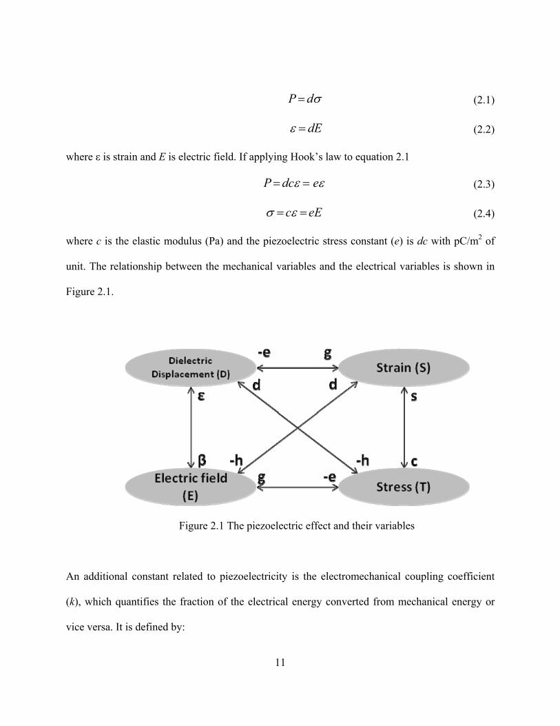
11
σdP= (2.1)
dE=ε (2.2)
where ε is strain and E is electric field. If applying Hook’s law to equation 2.1
εε edcP == (2.3)
eEc == εσ (2.4)
where c is the elastic modulus (Pa) and the piezoelectric stress constant (e) is dc with pC/m2 of
unit. The relationship between the mechanical variables and the electrical variables is shown in
Figure 2.1.
Figure 2.1 The piezoelectric effect and their variables
An additional constant related to piezoelectricity is the electromechanical coupling coefficient
(k), which quantifies the fraction of the electrical energy converted from mechanical energy or
vice versa. It is defined by:

12
energymechanicalinputenergymechanicalfromconvertedenergyelectricalk
energyelectricalinputenergyelectricalfromconvertedenergymechanicalk
=
=
2
2
(2.5)
By introducing Barium Titanate Oxide (BTO), piezoelectric ceramics were developed,
and their commercialized applications have expanded to include high voltage sources, wave
filters, delay line transducers, underwater sound and ultrasonic power, acoustic speakers, ink-jet
printer heads, and various types of sensors [19, 20].
Piezoelectric materials have several forms, including polycrystalline, single crystalline
ceramics, polymers, thin films, and composite films between polycrystalline and polymer. These
materials should be chosen considering the desired frequency and fabrication process. The single
crystalline ceramics include α-SiO2 (Quartz), LiTaO3, LiNbO, etc. and have high piezoelectric
properties, but their synthesis is limited by size and the cost of the substrate [21]. The
piezoelectric polymer and composite polymers include the PVDF families, PZT-PVDF (d33=25
pC/N) [22], PZT-epoxy (d33=80 pC/N) [23], etc. While they show high piezoelectric properties,
the synthesis of the materials is limited by size and cost. Now, most material studies for
piezoelectric applications are focused on polycrystalline ceramics such as ZnO, AlN, PZT, doped
PZT, and BaTiO3.
The piezoelectric effect originates from the symmetry of the crystal structure. Only non-
symmetric structures can make displacement of gravity in the negative or positive charge under
stress. The 32 crystallographic point groups have 11 centrosymmetric and 21 non-
centrosymmetric structures, and 20 piezoelectric groups are involved in non-centrosymmetrics.

13
Piezoelectricity is a directional property between stress and discharge, so piezoelectric
constants (d) have different values in different directions. The relationship should be considered
in three dimensions (3D) with tensor notation. The Hook’s law in three dimensions can be
expressed as
klijklij c εσ = (2.6)
where σ is stress, ε is strain, and c is elastic modulus. Since the stress and strain can be expressed
by a matrix, the tensor notation will be exchanged by a matrix notation. For example, the ij and
kl will be substituted by p and q. When i, j, k, or l has 1,2, or 3, p and q have 1, 2, 3, 4, 5, and 6.
Their relationships are shown in Table 2.1.
Table 2.1 Relationship between tensor notation and matrix notation
j i 1 2 3
1 1 6 5
2 6 2 4
3 5 4 3
Piezoelectricity can be mathematically described by a constitutive equation given by equation
(2.7) [19]
kEikqiqi
kkpqEpqp
ETdD
EdTsS
ε+=
+=
(2.7)

14
kTikqiqi
kkpqDpqp
DTgE
DgTsS
β+−=
+=
(2.7)
where S is the strain component, T is the stress component (N/m2), E is the electric field
component (V/m), D is the electric displacement component (C/m2), s is the elastic compliance
constant (m2/N), d is the piezoelectric constant (m/V or C/N), ε is the dielectric constant of the
piezoelectric material (F/m), g is the piezoelectric constant (V·m/N or m2/C), and β is the
impermittivity components (m/F). The superscript denotes a constant and zero condition of
notation for measurement.
A cantilevered energy harvester has in-plane strain on the piezoelectric film coated on the
structure in this study. The piezoelectric film has top and bottom electrodes that collect the
discharge in the normal direction of the strain. The constitutive equations used in this
configuration become
3331313
3311111
ETdD
EdTsS
E
E
ε+=
+=
(2.8)
and the sandwiched electrode between piezoelectric film with a cantilever structure use the 31
mode of piezoelectricity. We mainly consider constants of d31 and ε33.
2.1.2 Piezoelectric materials for energy harvesters
The energy harvesters require very high piezoelectricity, which is an inherent property of
materials, and the performance of the device is seriously affected by piezoelectric materials.
When the energy harvester is miniaturized by a MEMS process, the successful integration of

15
piezoelectric materials in thin film scale should be follow. The common piezoelectric thin films
such as the lead zirconia titanate (PZT) family, zinc oxide (ZnO), aluminum nitride (AlN),
PVDF, and BaTiO3 (BT) have been used for piezoelectric applications. Piezoelectric properties
are indicated by a piezoelectric coefficient (d) and a coupling coefficient (k), which relates strain
to electric field and the ability to convert mechanical energy to electrical energy or vice versa.
The typical values of k for unbounded piezoelectric materials are listed in Table 2.2.
Table 2.2 Coupling coefficient values of typical piezoelectric materials
Materials Coupling coefficient (k)
Quartz 0.1
ZnO 0.33
BTO 0.4
PZT 0.5 ~ 0.7
The piezoelectric constant in thin film scale, however, has different values when
compared to bulk materials, since the film is clamped on the substrate. The effective e31 and d33
for the thin film can be estimated by equations 2.9 and 2.10 [2].
3333
1331
1211
3131 e
cc
ess
de E
E
EE −=+
= (2.9)
311211
1333
33
3333
2d
sss
dce
d EE
E
E +−== (2.10)

16
PZT films have been chosen as a transducer layer for energy harvesting devices due to
their excellent electromechanical properties with high piezoelectric constants and
electromechanical coupling coefficients. They have been compared with other materials such as
ZnO, AlN, and poly(vinylidene fluoride) (PVDF), as shown in Table 2.3 [24-29]. The
piezoelectric constants in Table 2.3 are typical values of films less than 1 µm. Under a given
force on a cantilever, the stress on the surface of the structure is different depending on the
Young’s modulus of the materials. For example, polymer PVDF has a low Young’s modus and
makes a larger displacement on structures as compared to others. In this study, a thick Si
membrane supports the piezoelectric film so that the stress is not changed much depending on
the piezoelectric materials. Stiff silicon layers govern the displacement and stress on the surface.
PZT was chosen only considering its conversion efficiency.
Table 2.3 Comparison of piezoelectric coefficients of the representative materials in thin film
ZnO AlN PVDF PZT (x=0.48)
d31 (pC/N) -2.3~-4.7 -2 -8 -40~-94
k31 (CV/Nm) 0.19 0.12 0.22~0.31
d33 (pC/N) 7.5~12.4 3.4~5.1 30~33 90~223
k33 (CV/Nm) 0.28~0.41 0.21 0.16 0.49~0.67 The values vary in terms ofadditives, process conditions, and thickness (< 1 µm)
2.1.3 Lead Zirconate Titanate (PZT)
The perovskite structure of PZT consists of oxygen and small Ti or Zr atoms in
symmetrical octahedral sites, and Pb cations occupying dodecahedral sites, as shown in Figure
2.2.

17
Figure 2.2 Perovskite structure
The PZT shows that its crystal structure depends on the temperature, as well as the ratio
between Ti and Zr, as shown in Figure 2.3. Above the Curie temperature, the solid solution of
PbZrO3 and PbTiO3 shows a paraelectric cubic structure. The Curie temperature is the limited
temperature of the piezoelectric PZT material, and it ranges from 510 K to 800 K. The cubic
perovskite structure is distorted below the Curie temperature into a rhombohedral phase for Zr-
rich compositions or a tetragonal phase for Ti-rich compositions. The Curie temperature (Tc) is a
transition temperature of ferroelectricity and is defined as ε = C/(T-Tθ), where ε is the
permittivity, C is the Curie constant, and Tθ is the Curie-Wiess temperature. As the composition
of Zr or Ti, the PZT has a different phase between the rhombohedral and tetragonal ones. The
boundary of those two phases is called the morphotropic phase boundary (MPB) around the
Zr/Ti composition of 0.52/0.48. The tetragonal structure has six <100> polarization directions
and the rhombohedral structure has eight <111> polarization directions. The maximum
piezoelectric and dielectric constants are commonly observed at MPB due to high probability of

18
polarization, and they are more sensitive to the composition than to the temperature because the
MPB is very vertical.
Figure 2.3 Phase diagram of PZT [30]
2.1.4 Poling & depoling
When the material becomes ferroelectric with losing its symmetry, small-sized cations
(Ti4+ or Zr4+) move to the stable sites, which are determined by the minimum free energy through
the distortion of the structure. These movements enable charge separation and spontaneous
polarization.
The fabricated ferroelectric films have spontaneous polarization, but they do not show
ferroelectric behavior. Since the electric dipoles are randomly oriented before applying an
external electric field on PZT, the net polarization is zero. The uniform electric field or strain is

19
applied to rearrange the dipoles and obtain ferroelectric behavior. This is called “poling,” and the
dipole movement with poling is shown in Figure 2.4.
Figure 2.4 The dipole moment during the poling process
The localized dipole with uniform alignment is called the domain, and their boundary is
the domain wall. The neighbor domains should have different polarization directions, and the
motion of the domain wall is the origin of the ferroelectric mechanism, and the non-180 º domain
wall motion can be the origin of the nonlinear piezoelectric properties. It is known that the
polarization directions depend on the crystallographic direction as shown in Figure 2.5. The
tetragonal structure makes two kinds of polarization in antiparallel and perpendicular directions
that refer to the 180º and 90º domain walls, respectively. The rhombohedral structure also
provides more spontaneous polarization in the diagonal directions that refer to the 71 º, and 109 º
domain walls. It is known that the domain and domain walls are created to reduce the free energy
of the electrostatic and elastic energy in materials. Only the non-180 º domain walls contribute to
the reduction of the elastic energies so that the piezoelectric properties are dominated by them
[31, 32]. This is called the extrinsic contribution. The intrinsic contribution is the lattice
contribution from the displacement of each ion.

20
Cubic
Phase transformation
Tetragonal Rhombohedral
Figure 2.5 The shape change by the polarization as the crystallographic structures
Contrary to the poling of the materials, the dipoles rearrange to an equilibrium state as
time goes by without the electric fields or mechanical stress. This is called “depoling,” and the
piezoelectricity becomes degraded. The depoling of ferroelectric thin films is a factor to
determine their lifetime and functional degradation of piezoelectric applications. For example,
Kholkin et al. poled sol-gel deposited PZT film by UV. The piezoelectric constant and aging
(depoling) improve with poling time, temperature, and electric field [33]. They have saturated

21
values when poled over 100 oC and 600 seconds. The electric field should be high enough to
increase the active domains, but not breakdown the voltage because of the thickness of the films.
2.1.5 Piezoelectric mode (d33 & d31)
Randomly oriented PZT film can be polarized and produce electricity in the direction of the
electric field. The d33 (longitudinal) mode has the motion parallel to the electric field. The d31
(transverse) mode utilizes the motion perpendicular to the electrical field. In the d15 (shear)
mode, the electric field is perpendicular to the polarization and induces shear stain.
In bulk PZT (52/48) at MPB, d33 = 223 pC/N, d31 = - 94 pC/N, and d15 = 494 pC/N were
measured [34]. Although the largest motion can be generated from d15, the structure using d15 is
hard to build up. Therefore, the d33 and d31 mode is usually developed, as shown in Figure 2.6.
When the cantilever bends up and down, the strain and polarization occur in the direction of right
and left. The electrodes are placed in a transverse direction that is perpendicular to the
polarization direction. Figure 2.6(a) has the 31 mode. An Interdigital Electrode (IDE) is available
for the 33 mode where the electrodes collect polarization in a normal direction.
Figure 2.6 Electroe configurations of d31 and d33 for cantilever beam
F F
F F

22
The energy of the capacitor is expressed by E=CV2/2. Although the d33 mode has a dielectric
constant (d33) that is twice as large, the IDE design has a smaller charge density than that of d31.
The longitudinal mode has an incompletely coupled region with the d33 constant under the
electrode and induces a different stiffness due to non-uniform poling. While the output voltage of
the d31 mode is decided by the thickness of the PZT film, the configuration of IDE can regulate
the output voltage in the d33 mode. Table 2.4 shows the comparison between the d33 and d31
modes.
Table 2.4 Comparison between the d33 and d31 modes for energy harvesters
d33 d31
Pro - High dielectric constant - Easy output voltage regulation
- Large charge density - Easy control of PZT microstructure o
n Pt electrode
Cont. - High % loss factor
(wasted area under electrode) - Requires optimization of IDE - Complicated modeling due to IDE
- Low dielectric constant
The optimization of IDE should be executed considering the longitudinal poling to prevent
electrode loss. For example, it is intended that a narrow width of electrode is adequate due to the
small loss under the electrode area. The simulations for optimized IDE design were developed by
Finite Elements Analysis (FEA) [35, 36]. Knight simulated the maximum d33 polarization of
IDE, which is obtained when large spacing (s) between electrodes exists and when the
polarization is decreased by increasing the space between the finger electrodes/thickness of PZT
after a maximum value at 0.8. The width (Ws) between the electrode strips should be four times

23
longer than the spacing (s), and the polarization is dramatically decreased if spacing (s) is less
than 10 µm [36].
2.2 Electrical power management
The total system of self-power is divided between the piezoelectric energy harvester and
the storage circuit system as shown in Figure 2.7. When designing the energy harvester, its
efficiency is a major issue, and the link between the energy harvester and the managing circuit
should also be considered.
Figure 2.7 A schematic diagram of a standard energy harvesting system
The vibration source resonates the cantilevered energy harvester and makes cyclic stress
on the piezoelectric layer. Piezoelectric energy harvesters generate an AC current parallel to a
complex output impedance while the device structure resonates at the resonant frequency. Since
electronics requires stable DC voltage, the output from the energy harvester should be rectified
and regulated for the target electronics. The process signals are illustrated in Figure 2.9.

24
FiFigure 2.8 The signals during piezoelectric energy harvester system
The standard energy harvesting circuit is shown in Figure 2.9. The AC signal is rectified
by full-wave by Wheatstone Bridge and the filtering capacitance is followed to smooth the DC
voltage. The resistive load regulates the voltage. Since the generated electric output is mostly
low and intermittent to be provided to the electronics directly, accumulation or storage of the
electrical energy is required.
Figure 2.9 A standard energy harvesting circuit
The output voltage (Vp) generated from the energy harvester (EH) should be high enough
not to be blocked on the rectifier. The diode rectifier has its own threshold voltage, and the

25
power loss occurs through the diode proportional to its threshold voltage. The diode should be
selected considering power losses with low dissipation. The MOS transistor is a possible
application with the advantages of scaling down [37]. In the mean time, Vp should be high
enough but not too high to breakdown the circuits. The power losses occur through all circuit
elements and are constituted as a portion of Vp.
To maximize the power delivery, the impedance of the energy harvester should be
optimized to match that of circuits or vice versa. Piezoelectric energy harvesters produce low
current compared to the generated voltage. The matching impedance might reduce the power
losses on circuits. A higher current, moreover, will reduce the charging time on capacitors.
The electric circuit for piezoelectric energy harvesters has been developed considering
the energy harvester [38-40]. The circuits study predicts the electrical behavior of the
piezoelectric energy harvesting system considering the electrical load, the resonant frequency,
the damping effect, and the electromechanical coupling coefficient. One of the electric circuits
for the piezoelectric energy harvesting system called “Synchronized Switch Harvesting on
Inductor” (SSHI) was proposed [41]. SSHI consists of a switch and an inductor in serial
connection. The switch has a closed state when the transducer makes the maximum
displacement, and the inductance and capacitance of the piezoelectric film produces an oscillator.
The SSHI increases the output power effectively, but the quality factor of this nonlinear
processing circuit is still an issue on efficiency.

26
2.3 Piezoelectric MEMS energy harvester
2.3.1 Single piezoelectric MEMS energy harvester
The piezoelectric energy harvester in a bulk scale has been successfully verified as a
possibility to be a power source for self-sustained wireless sensors. Their large size, however,
restricts their integration into miniaturized wireless sensors.
In the early 2000s, researchers started to focus on the modeling and fabrication of a
piezoelectric energy harvester in a micro scale. Demir et al. reported the strain, deflection, and
generated output power for a power generator with a PZT membrane. They also investigated the
residual stress and compositional function of PZT thick film [42]. Lu et al proposed the modeling
of 31 mode micro power generators with films of both PZT and PZN-PT single crystal [43].
The reported prototype of MEMS energy harvesters are compared in Table 2.5. The
piezoelectric energy harvester based on a cantilever structure with a proof mass is widely used
due to its large strain at a given acceleration force and easiness to build up a low resonant
frequency. Marzencki et al. fabricated a cantilever-based energy harvester with an Si proof mass.
It seems that their energy harvester generated a relative low power of 0.038 µW due to the low
piezoelectric properties of AlN film [44]. Later, they integrated the power management circuit on
multiple cantilevers. Multiplied voltage was generated throughout the capacitance load, but
power was low, in the tens of nW at 0.4 g acceleration condition [37, 45]. Jeon et al. first
developed a PZT-based piezoelectric energy harvester using 33 mode by using interdigitated
electrodes. They controlled the residual stress by selecting an oxide buffer layer to prevent
bending of the cantilever. Their device generated about 1 µW power and 2.4 DC voltage after
rectifying and storing at 13.9 kHz and 10 g of resonant frequency and acceleration [46]. The

27
optimal resistance was 5.2 MΩ due to a small area of IDE configuration as compared to that of
the electrode plate in 31 mode. Fang et al. aligned a Ni proof mass at the end tip of the PZT
cantilever for a larger displacement. A thick PZT transducer layer with top and bottom electrode
plates generated 2.16 µW of output power at 1 g and 609 Hz conditions [47]. The resonant
frequency of their energy harvester was reduced as compared to previous ones due to the thick
beam structure with the silicon layer, but it is still higher than ambient vibration sources. The
alignment of the Ni mass is not compatible for the MEMS process and restricts further
miniaturization. Lee et al. compared the 31 mode and 33 mode using 11 µm thick aerosol
deposited PZT film [48]. While the 33 mode energy harvester generated 2.3 V with resistive load
and 0.35 µW, the 31 mode device generated 1.6V with resistive load and 1.1 µW under 1 g
acceleration force and 256 Hz of resonant frequency. The aerosol deposited thick PZT induced
serious bending on the cantilevered structure, and it seems that the film has a large leakage due
the microstructure of the aerosol deposited films based on its remanent polarization value of less
than 10 µC/cm2. Elfrink et al. generated a high output power of 60 µW using a large silicon mass
and an AlN film under 2 g acceleration force and 572 Hz of resonant frequency [49]. Their
energy harvester generated about 2 V through a load of 500 kΩ. They show that AlN is a viable
choice for piezoelectric energy harvesters due to its low dielectric constant and simple deposition
techniques. The low dielectric constant induced a high optimal resistive load and a relative high
voltage as compared with that of the PZT film, but it has a large discrepancy when matching
impedance with circuits. Shen et al. [50, 51] generated a moderate level of power of 2.15 µW
and 160 mV under 2 g acceleration force and 465 Hz. Although the low impedance of 6 kΩ
generated a relatively high power, its low output voltage is still a limitation for circuitries under
the typical threshold voltages of MOFET transistors. The later report of a similar structure shows

28
less output power. It seems that this discrepancy is caused from unstable film properties of PZT.
A laser machined power generator in a few mm size of scale was tried, but the process is
inherently limited to scaling down and showed a low power density at 301 µW/cm3 [52].
Table 2.5 The comparison of reported MEMS energy harvesters
Author Device cantilever/mass Mode Conditions
(ms-2 / Hz) Power (μW)
Power density
(μW/cm3)
Marzencki et al. AlN / Si 31 4.9 / 204 0.038 10
Marzecki et al. AlN / Si 31 39.2 / 1368 1.97 3569
Y.B.Jeon et al. PZT / (Su-8) 33 106 / 13.9 K 1 37,037
Fang et al PZT / Ni 31 9.8 / 608 2.2 10,843
B S Lee et al. PZT / Si 31
33 9.8 / 255.9 9.8 / 214
2.765 1.288
6513 2105
Elfrink et al. AlN/Si 31 19.6 / 572 60 ~5214
Shen et al. PZT / Si 31 19.6 / 465 7.36 / 184
2.15 0.32
3,272 416
2.3.2 Multi-beam arrayed piezoelectric MEMS energy harvester
The single cantilever has a limitation of low output power, low voltage for the threshold

29
of circuitries, or low current in recent technology, which is insufficient for wireless sensor
networks. Moreover, their narrow operation frequency range also restricts their uses under the
uncertainty of the frequency of ambient vibration sources. The cantilever array was proposed to
solve these issues, and the later one has been introduced in bulk and MEMS scale to widening
working frequency regions.
The cantilever-based energy harvesting arrays were introduced in bulk scale by Ferrari et
al. At the certain frequency of resonating, the measured signals from the open circuit definitely
created interference. For three cantilevers designed to be resonated at 113 Hz, 183 Hz, and 281
Hz of frequency, their output signals were rectified and charged to the capacitor individually
[53]. Liua et al. first introduced micro multi-array power generators for the broadband working
frequency. They used PZT thin film and aligned an Ni proof mass at the end of the tip. Three
cantilevers generated 2.55 µW, 2.1 µW, and 1.87 µW at their own resonant frequency. Their
MAPG covers the frequency range from 226 to 234 Hz, and they generated 3.98 µW and 3.93
DC output voltage charge in capacitor at the 229 Hz of frequency [54].
With the output power, the voltage and current should be regulated when connecting to
the power management circuit. In bulk scale, multi layers of piezoelectric transducer layers may
regulate the output voltage and current, but its scheme is hard to realize due to limitations of film
technology, such as internal stress and keeping piezoelectric properties for multi layers. In this
study, a cantilever array design is used for regulating the output voltage or current with the
increase of output power.
31
CHAPTER 3 INTEGRATING PIEZOELECTRIC THIN FILM ON SILICON WAFER
The properties of the piezoelectric layer are important to construct a highly efficient
energy harvester. Since the properties of the piezoelectric layer are influenced by the deposition
method and the types of layers and substrate, an investigation of these parameters was executed
in these issues.
3.1 Film characterization
The dielectric and ferroelectric properties of the PZT thin films were characterized by an
impedance analyzer (HP 4192A) and a TF Analyzer 2000 (aixACT, FE-module). For dielectric
properties, four different sizes (0.01, 0.04, 0.09, 0.25 mm2) of square electrodes were patterned
on PZT and the dielectric constants were measured with the dielectric loss. The hysteresis loops
of PZT films were characterized for both the small square electrodes and the actual device to
evaluate and inspect the piezoelectric performance of each PZT layer after fabrication. With
measured remnant polarization and dielectric constant, the piezoelectric coefficient can be
roughly estimated by following Equation 3.1.
(3.1)
32
where Q12 (-3.1x10⁻² m4C-2) is the electrostrictive constant, is permittivity of vacuum, εs is
relative dielectric constant, and Pr is remnant polarization.
The deposited PZT films were characterized by inspecting their microstructures and
crystallographic orientations using a Scanning Electron Microscope (SEM, JEOL) and X-ray
Diffraction (XRD)
3.2 Thin film deposition
Various deposition methods for ferroelectric thin films have been investigated by many
researchers such as chemical solution deposition (CSD), metalorganic chemical vapor deposition
(MOCVD), sputter, pulsed laser deposition (PLD), and molecular beam epitaxy (MBE)
deposition. Besides the film properties, the scalability to the wafer size is most important when
integrating the films on MEMS devices. Their characteristics are summarized in Table 3.1.
Table 3.1 Comparison of deposition methods for ferroelectric materials
CSD MOCVD Sputter PLD MBE
Mechanism Chemical reaction
Chemical reaction
Momentum energy
Thermal energy
Thermal energy
Deposition rate Low Moderate Low Moderate High
Scalability Large Large Large Small Large

33
Since our energy harvester requires high efficiency of conversion between strain and
electricity, the PZT film was chosen based on the reported materials constant in Table 2.1. To
obtain best piezoelectric properties of PZT films, precise control of the PbZr1-xTixO3 composition
is required, which is strongly influenced by the thin film process. Sputtering, PLD, and CSD are
commonly used to grow perovskite PZT films with a high piezoelectric coefficient. The sol-gel
derived PZT deposition is widely used for thin films, since its films show a high coupling
coefficient with precise control of composition and the process is simple and cheap [55-58]. The
typical process of sol-gel deposition is shown in Figure 3.1. The sol-gel deposited films are
highly affected by precursor chemistry, deposition conditions, and heat treatment conditions.
This study experimentally investigates the effect of heat treatment and interaction with
conjugated films.
Figure 3.1 Typical sol-gel derived chemical solution deposition (CSD) process.
3.3 Chemical Solution Deposition (CSD) of PZT film
The PZT film in this study was deposited by CSD method to obtain a high stoichiometry
composition. It is common that the piezoelectric properties of thin film cannot exceed that of

34
bulk PZT due to limited thickness and internal stress during clamping of the film on substrate.
Many researchers have investigated the development of PZT thin film in recent years, and CSD
is the most used method for stoichiometry [55-58]. The PZT film study was performed on the
composition, substrate effect, thickness, and heat treatment.
We should design the PZT considering the composition of Zr/Ti and the crystallographic
orientation as the application of the energy harvester that requires a high piezoelectric coefficient
(dij). Pb(ZrxTi1-x)O3 shows maximum piezoelectricity at the rhombohedral-tetragonal phase
boundary (x=0.48), which is the so-called morphotropic phase boundary (MPB) in Figure 2.3.
In Figure 3.2, the coupling coefficient and piezoelectric constant have maximum values at
52% of zirconium. It is reported that the PZT thin films show the highest piezoelectric
coefficient (d31) in the 31 mode at the MPB composition of 53% Zirconium and 47% titanium
and (111)-textured orientation [59]. The film studies in this paper are performed based on this
composition.
Figure 3.2 The schematic changes of coupling coefficient and piezoelectric constant as mole % of Zr [60]

35
A PZT (Pb:Zr:Ti=110:52:48) solution of commercial product from Inostek. Inc. was
coated on platinized silicon wafers by chemical deposition as 12 layers, which make about 1 µm
thickness. The solution was dropped on the entire wafer with filtering probable particles (larger
than 0.2 μm) in solution, and it was coated by spinning at 4000 rpm for 20 second with a high
acceleration rate. Each layer was pyrolyzed at 350 ºC for 10 minutes on a hot plate or furnace at
the ambient condition and annealed at 650 ºC for 15 minutes by Rapid Thermal Annealing
(RTA) or in a furnace. The PZT film was finally annealed at 650 ºC for 30 minutes, and its
process is shown in Figure 3.3.
Figure 3.3 Process flow of PZT chemical deposition
A platinum (100nm) layer was used for the bottom electrode due to its stability at high
temperature annealing. The bottom Pt was deposited on the amorphous SiO2, which played the

36
role of electrical barrier. To enhance the adhesion between the Pt and SiO2 interlayers, Cr, Ta,
and Ti were used.
3.3.1 Analysis of PZT thin film on Pt substrate
Sol-gel derived PZT film was deposited on (111) textured PT electrodes. The properties
of the PZT films that were deposited on the substrate of Pt(120nm)/interlayer/SiO2(500nm) were
investigated by XRD and SEM for their microstructure, and their electrical properties were also
investigated with PE hysteresis loop and dielectric constant. It is a general agreement that (100)
and (111) preferred orientation PZT film is observed on the Pt (111) substrate. The Pt was
deposited by a sputter system under the conditions of 100W DC power for 360 second, and 5
mTorr. The crystallographic orientation of Pt was firstly inspected as shown in Figure 3.4.
20 30 40 50 60 70 80
Pt (
111)
2θ
Inte
nsity
Figure 3.4 XRD data of as deposited Pt/Ti (120/10 nm) by sputtering

37
When considering minimal interface energy between PZT and Pt, PZT (111) orientation
is more favorable on Pt (111) due to lattice matching [61, 62]. Moreover, the intermetallic
interface layer between PZT/Pt created by Ti diffusion through Pt energetically enhanced the
(111) orientation of the PZT nucleus [63, 64]. The sol-gel process, however, has various factors
that affect the film properties and its crystallographic orientation, such as the solution chemistry,
substrate orientation and microstructure, and heat treatment [65, 66].
20 30 40 50
PZT
(200
)/(00
2)
Pt (
111)
PZT
(111
)
PZT
(110
)
PZT
(100
)/(00
1)
2θ
Inte
nsity
Figure 3.5 PZT/Pt film analysis by XRD
PZT (Zr=48%) whose thickness is 500 nm was deposited on Pt/Ti/SiO2 substrate with
300 ºC pyrolysis on a hot plate and 650 ºC annealing in a tube furnace. The obtained orientation
of the PZT film is a mixture of (100), (111), and (110), but the (100) orientation is the most
preferred in Figure 3.5. The formation of (100) preferred orientation PZT is not fully understood
yet. While the (111) texture of PZT is promoted by metastable interfacial layer (Pt5-7Pb), the
(100) texture is enhanced by the pyrolysis temperature and time, and the texture can be stronger

38
as the thickness increases due to a lower interfacial energy and a faster growth rate [67-69]. No
pyrocholore phase around 29º appeared on the XRD analysis. It is reported that (100) films show
higher piezoelectric properties at the 31 mode than the (111) orientation films do [59]. Figure 3.6
shows the microstructure of the PZT film, which has a dense and columnar structure with ~100
nm diameter of grain size. The roughness of the PZT film was measured as 2.5 nm by AFM
anlaysis.
Figure 3.6 SEM image of PZT film
3.3.2 Adhesion layers effects on the electrical properties of PZT
The adhesion layers used between SiO2 and Pt were studied, and their effects on the
electrical properties of PZT layer were investigated. It is known that the adhesion layers
diffuse up through the Pt grain boundaries and affect the properties of PZT film during heat
treatment [63]. It is assumed that the thin TiO2 layer plays the role of seeding layer for PZT
39
nucleation. First, the thickness of the adhesion layer was investigated. Thickness of 10, 40, and
100 nm Ti films were used for Pt bottom electrodes, and then PZT was deposited with the
same conditions. Ti adhesion layers gave sufficient levels of adhesion in the tape test and the
ultrasonic test in all thicknesses. The P-E hysteresis loops were measured for each sample, as
shown in Figure 3.17. The thinnest Ti film shows the highest piezoelectricity of ~21.5 μC/cm2
in remanent polarization, as shown in Figure 3.7, while PZT films using thicker Ti adhesion
layers show ~15 μC/cm2 after correcting asymmetry of loop. It seems that the limited source of
the Ti layer impeded diffusion to the PZT layer while the thick films provided an excess of Ti
on the Pt electrode.
-15 -10 -5 0 5 10 15
-40
-30
-20
-10
0
10
20
30
40Polarization (uC/cm2)
Voltage (V) T10 T40 T100
Figure 3.7 PE hysteresis loops of PZT films deposited on different thicknesses of adhesion layers
Various materials (Ti, Cr, and Ta) were deposited with 10 nm of thickness and PZT
deposition followed. The polarizations and dielectric constants of the PZT films on different
adhesion layers were measured as shown in Figure 3.8 (a) and (b). While PZT films with Cr
and Ta adhesion layers show very low remanant polarization of 6 μC/cm2 and 11 μC/cm2, the

40
film with Ti adhesion layer showed higher values up to 21.5 μC/cm2. When comparing the
dielectric constants of PZT films on different adhesion layer, the films with Ti and Ta adhesion
layers have a high value of about 1100. The piezoelectric constants (d) were calculated from
remanant polarizations and dielectric constants using equation 3.1, and shown in Table 3.2.
-10 -5 0 5 10
-40
-20
0
20
40Polarization
(μC/Cm2)
Volatage (V)
PZT_Ti PZT_Ta PZT_Cr
(a)
-10 -5 0 5 10
400
600
800
1000
1200
1400
Die
lect
ric C
onst
ant
Voltage (V)
PZT_Ti PZT_Ta PZT_Cr
(b)
Figure 3.8 Substrate effect on electrical properties of PZT films. Adhesion layers deposited between SiO2 and bottom Pt, and their effects described by: (a-b) Ti, Cr, and Ta have different effects on PZT
Table 3.2 Pr, εr, and d31 of PZT films deposited on different adhesion layers
Material Pr (µC/cm2) εr d31 (pC/N)
Cr 5.95 838 -27
Ta 11.28297 1193 -74
Ti 21.5 1184 -140
PZT films on Ti and Ta adhesion layers had strong (111) orientation, but PZT films on Cr
adhesion layers showed random orientations with both (111) and (110) orientations. When it is

41
assumed that the adhesion materials diffuse up and affect the nucleation of the PZT film,
oxidized Cr may restrict the (111) oriented nucleation. In MPB composition, mixture
orientations of (111) and (100) have higher dielectric constants than that of single-oriented film
due to multiple polarization directions [70]. Figure 3.8 (b) and Figure 3.9 (a) show opposite
results. It seems that Cr obstructed the oxide on the ferroelectric PZT film and decreased the
dielectric constant [71]. In Figure 3.8 (a), the loop of the PZT/Pt/Cr was shifted because of a
non-symmetric electrode configuration due to a second phase of Cr.
2 0 3 0 4 0 5 00
1 0 0 0 0
2 0 0 0 0
Pt (1
11)
PZT
(200
)/(00
2)
PZT
(111
)
PZT
(110
)
PZT
(100
)/(00
1)
Inte
nsity
2 θ
T a C r T i
(a)
(b)
(c)
(d)
Figure 3.9 XRD and SEM analysis of PZT film on different adhesion layer: (a) XRD anlaysis,
(b) Ti, (c) Cr, and (d) Ta adhesion layers

42
PZT film on the Ti and Ta adhesion layers had similar grain size, but the film on the Ta
has a little more uniform grain size. The (111) preferred orientation of PZT may have a smaller
grain size than that of the (100) oriented PZT. The small grain size on Cr seems to be attributed
to its homogeneous nucleation and granular microstructure. In Figure 3.10, the cross section
views of PZT films on Cr and Ti can be compared in granular and columnar forms,
respectively. The hypothesis is that Cr diffuses and creates precipitation on each layer of PZT
so that it gives a homogeneous nucleation site. PZT film on the Ti and Ta adhesion layers had
a similar grain size, but the film on the Ta has a little more uniform grain size.
(a) (b)
Figure 3.10 Angle view of PZT thin film on Cr and Ti adhesion layers: (a) Cr and (b) Ti
3.3.3 Heat treatment effects
The piezoelectric properties of PZT are affected by the heat treatment conditions of
pyrolysis and annealing. In CSD deposition, the growth of PZT on a Pt substrate is mainly

43
influenced by precursor chemistry and substrate conditions [65]. Furthermore, the pyrolysis and
annealing temperature are important in the formation of the preferred orientation. During the
pyrolysis heat treatment (the typical range of temperature is 200 to 400oC), some reactions
occured, such as formation of volatile organic species (thermolysis), formation of volatile
organic molecules by combustion (pyrolysis), dehydration for OH groups, and formation of
carbonate (M-O-CO2, oxidation). Since the films shrink during pyrolysis with rapid heat
treatment, the films have a lot of internal stress, which can induce cracks. The stress can be
controlled by keeping the viscoelastic gel on longer during heat treatment by adjusting the
reactivity of precursors [72]. After the film reaches its amorphous structure during pyrolysis,
crystallization is required by an annealing heat treatment. The nucleation and growth mechanism
of the films can be understood by kinetic and thermodynamic driving force. The mobility of
atoms, reactivity control by precursor chemistry, and the residual organics and constituent
influence the microstructure and orientation of oxide films deposited by CSD during the entire
process.
In this section, the pyrolysis heat treatment effect was inspected during CSD deposition.
The hot plate is usually used for the pyrolysis process of gel formation of PZT [73]. The tube
furnace and hot plate were used to compare the isothermal effect on the pyrolysis process. A
total of six layers of PZT (500 nm) were deposited on Pt/Ti, and they were pyrolyzed by a
conventional furnace and hot plate. All samples were annealed at 650 oC for 15 minutes after the
pyrolysis process. Temperatures of 237, 290, and 330 oC on the hot plate were investigated,
which was calibrated on the PZT surface by a thermocoupler. The remanant polarizations of the
three temperature points show similar, but low values in Figure 3.11(a). When comparing other
films pyrolised using a conventional furnace and tube furnace, it is about two times less, as

44
shown in Figure 3.11(b) and (d). The reason seems to be that the hot plate makes a higher
temperature gradient than the other methods and the surface of the PZT layer is exposed to
ambient air conditions. The dielectric constant of the PZT film pyrolised using a hot plate
showed the smallest value, seen in Figure 3.11(c).
220 240 260 280 300 320 34010
20
30
40
50
60
P
max
(μC
/cm
2 )
Pyrolysis temperature (oC)
Hot plate Box furnace Tube furnace
-20
-10
0
10
20
Rem
nant
pol
ariz
atio
n
Pyrolysis conditions
(a) (b)
-10 -5 0 5 10
400
500
600
700
800
900
1000
1100
1200
Dielectric constant
Applied voltage (V)
Hotplate 10K Box furnace 10K Tube furnace 10K
-30 -20 -10 0 10 20 30
-60
-40
-20
0
20
40
60Polarization (μC/cm2)
Voltage (V)
Hot plate Box furnace Tube furnace
(b) (d)
Figure 3.11 Electric properties of PZT films using different heat treatment methods: (a) as
temperature on hotplate (b) Pr, (c) dielectric constant, and (d) PE loop as heat sources
While the strong PZT (100) was shown when the film was pyrolized by furnace, the film
using a hotplate showed strong (111) and (110) orientations. As mentioned earlier, PZT (100)
45
has large remanant polarization and dielectric constant.
20 30 40 50P
ZT (2
00)/(
002)
Pt (
111)
PZT
(111
)
PZT
(110
)
PZT
(100
)/(00
1)
2θ
Inte
nsity
20 30 40 50
Inte
nsity
2θ
PZT
(110
)
PZT
(111
)
Pt (
111)
(a) (b)
Figure 3.12 XRD analysis of PZT film pyrolised using (a) furnace and (b) hotplate
3.3.4 PZT thickness effects
The piezoelectric properties of PZT film may be restricted due to the constraint on the
substrate surface when the film is very thin. If the thickness of the film is large enough, the effect
of the substrate can be negligible for the piezoelectric properties. While thick PZT film generates
more power from piezoelectric energy harvesters, the thickness of PZT film is limited in film
technology in MEMS devices by cost and quality. While many studies are working on increasing
the PZT thickness [69, 74-76], in this study the thickness effect of around 1µm was found not to
lose the superior piezoelectric properties of PZT due to it small thickness. PZT films that have
500nm, 750nm, and 1000nm thicknesses were prepared by a CSD technique that repeated the 6,

46
9, and 12 times, respectively. As the thickness increased, the crystallographic orientation was not
changed with strong PZT (111) peak, as seen in Figure 3.13.
20 30 40 500
5000
10000
15000
20000
Pt (1
11)
PZT
(200
)/(00
2)
PZT
(111
)
PZT
(110
)
PZT
(100
)/(00
1)
2 θ
Inte
nsity
500nm 750nm 1000nm
Figure 3.13 XRD analysis of PZT films with different thicknesses
Electrodes of 0.25 mm2 were patterned on the PZT film, and the PE hysteresis loop and
dielectric constant were measured, as seen in Figure 3.14. Although the dielectric constant
decreased a little, the remanant polarization was constant as the thickness decreased. As the
thickness increased, the coercive field increased due the large distance between the electrodes. It
seems that a further increase of PZT film does not improve its piezoelectric properties but
increases the power by a large volume. PZT film of 500 nm still kept reasonable piezoelectric
properties without an effect on substrate clamping.

47
-30 -20 -10 0 10 20 30
-60
-40
-20
0
20
40
60
Voltage (V)
Polarization (uC/cm2)
500nm 750nm 1000nm
1000 10000
0
200
400
600
800
1000
1200
Die
lect
ric c
onst
ant
Frequency (Hz)
500nm 750nm 1000nm
Figure 3.14 PE hysteresis loop and dielectric constant as frequency for the PZT films with
different thicknesses

49
CHAPTER 4 DESIGN AND FABRICATION OF MEMS ENERGY HARVESTER
4.1 Design
The structure of piezoelectric energy harvesters should be designed to create a higher
strain on the piezoelectric transducer layer. The representative structures in MEMS are
categorized into three configurations: diaphragm, bridge, and cantilever, as shown in Figure 4.1.
The cantilever structure was chosen to create a high efficiency energy harvester in this study,
since the freestanding structure with one-side clamping shows the highest strain under a seismic
force among them.
(a) Diaphragm (b) Bridge (c) Cantilever
Figure 4.1 Illustration of common configurations of pMEMS structures
In this study, the cantilevers were designed with a silicon proof mass at the end of the tip and a
silicon support layer under the beam, as shown in Figure 4.2. The silicon mass

50
puts a larger force and strain on the beam during seismic accelerating as well as decreasing the
resonant frequency of the structure. The proof mass is easily built up by the dry etching process,
while integration of the mass by aligning is more complex and costly [77, 78]. Very strong
silicon-oxygen covalent bonds create a high mechanical strength between the beam and mass.
The silicon support layer gives mechanical strength to the structure and enables the energy
harvester to operate at a high accelerating force. The bending of the cantilever due to residual
stress between films can be prevented by adding a Si support layer.
Figure 4.2 Schematic of cantilever energy harvester with proof mass and the notation of dimension
4.1.1 Resonant frequency
The cantilever beam should be designed to achieve maximum output power at the
expected resonant frequency of the applications. At the given film structure, the dimensions of
the cantilever and mass dominantly decide the resonant frequency of the energy harvester. Since
a small deviation from the resonant frequency induces a large reduction of output signals due to
narrow resonant peak of MEMS devices, the energy harvester requires precise modeling to
determine their dimensions for the expected resonant frequency.
The resonant frequency (fr) can be calculated by Equation 4.1[79]

51
er m
Kfππ
ω21
2== (4.1)
where ω is the angular frequency, K is the spring constant at the end-tip of the cantilever, and me
is the effective mass of the cantilever. The resonant frequency of the cantilever without a proof
mass can be expressed by Equation 4.2
mEI
lv
f nn ′= 2
2 12π
(4.2)
where fn is the nth mode resonant frequency; υn is the nth mode eigenvalue; l is the length of the
cantilever; E is the modulus of elasticity; I is the area moment of inertia about the neutral axis,
and m’ is the mass per unit length of the cantilever beam.. The equation 4.2 can be express in
terms of bending modulus per unit width Dp by
mD
lv
f pnn 2
2 12π
= (4.3)
sspp ttm ρρ += (4.4)
where the mass per unit area m is calculated by the thicknesses and densities, ρp and ρs are the
densities of the PZT and substrate, respectively, and the dimensions of the cantilever structure
are denoted in Figure 4.2. The bending modulus (Dp) is a function of Young’s modulus and
thickness and is expressed by [80]
)(12)322(2 224242
sspp
spspspspssppp tEtE
ttttttEEtEtED
+++++
= (4.5)
where Ep (PZT) and Es (Si) are Young’s moduli of two materials and their thicknesses, tp and ts,
on the tip of the cantilever.
When the point proof mass is located at the end tip of cantilever and its size is smaller
than the length of cantilever, the resonant frequency can be approximately expressed by [80]

52
mm
Kvf
e
nn Δ+=
π2
2'' (4.6)
where 236.0/32'2nn vv = , and K and me are the effective spring constant and effective mass,
respectively. The effective mass (me) is given by 0.236mwl considering axial velocity in length,
but not in width when w << l. The effective spring constant (K) can be expressed by
3
3l
wDK pp= (4.7)
The Si proof mass is distributed through the large area rather than at the point at the end
tip of the cantilever. When the center of the mass has a concentrated point load, its distance is
lm/2 from the end tip. The effective spring constant at this location can be expressed by [81]
3'
2/ ⎟⎟⎠
⎞⎜⎜⎝
⎛−
=mlllKK (4.8)
The resonant frequency of a unimorph cantilever with a proof mass can be calculated by
substituting the effective spring constant (K’) for spring constant (K) of Equation 4.6. It is
expressed by
337
32
)2/(236.0)2/(236.0
2 mp
mppnn llmllmw
llDwf
−Δ+−
=πν
(4.9)
where mmmm hwlm ρ=Δ .
The low resonant frequency and large displacement of the cantilever beam is determined
by the configuration of a long beam or a large mass and/or a softer beam. Hence, the ideal design
for the piezoelectric energy harvester demands a high mechanical strength to the beam against
the vibration and high density mass for its efficiency. Although the polymer based piezoelectric
materials have flexibility, their low coupling coefficient could not satisfy the required output
results [28].

53
The material constants of thin film should be carefully decided to reduce the deviation of
resonant frequency due to different values in thin film scale and clamping effect between layers.
The Young’s modulus of PZT was measured by nano indenter and other values were surveyed,
as shown in Table 4.1 [82]. The cantilevers are designed in one direction on a wafer as (110).
Table 4.1 The material constants
pE )110(SE pρ sρ
160 GPa (m) 169 GPa (c) 7500 kg/m3 (c) 3100 kg/m3 (c)
(m): measured value, (c): calculated value
4.1.2 Strain on PZT film & Safety factor
Along with modeling resonant frequency, the mechanical strength of the cantilevered
beam was investigated during designing the energy harvester. As most artificial structures are
built up with an extra safety factor against predicted maximum stress, MEMS devices also
should be designed considering their safety factor. Most of the reported energy harvesters hardly
consider their mechanical strength. This section gives the way to estimate the safety factor of
cantilevered energy harvesters.
The mechanical strength of the cantilevered structure as the acceleration force was
investigated. The mechanical strength of the cantilever can be expressed by a safety factor, and
can be derived using Equations (4.11) to (4.15).

54
maxσσ ysS = (4.11)
IttM ps )2/(
max
+=σ (4.12)
323
121
122 sp
p
spp
pp twEEbtw
twI +⎟
⎟⎠
⎞⎜⎜⎝
⎛+= (4.13)
2sp tt
b+
= (4.14)
pmpm
p wll
mgllmgM2
)()
2(
2+++Δ= (4.15)
where σys is the yield strength or fracture strength of the weakest material, σmax the maximum
stress at the bended surface (mostly anchor area), M the moment of the cantilever with a proof
mass, and I the moment of inertia of the cantilever. The gravity point of the proof mass was
considered as a point mass for simplification of analysis.
4.1.3 Design consideration for low resonant frequency
When the materials of the cantilever structure are fixed, the resonant frequency is
dominantly decided by the configuration of size between the length and the mass as well as the
thickness of beam, as shown in previous sections. While the low resonant frequency of the
structure is very important for the energy harvester targeting a specific vibration source, its
mechanical strength and the stress on the PZT transducer layer should be highly considered for

55
the energy harvester. The stress is closely related to the output voltage, which can be expressed
by Equation 4.16 under open circuit condition.
pxxoc tgV σ31=
(4.16)
where g31 is piezoelectric voltage constant, σxx is stress in longitudinal direction, and tp is
thickness of PZT. The stress has a proportional relationship with the output voltage in
piezoelectric cantilevered energy harvesters.
Weight of mass effect
The resonant frequency was plotted as a function of proof mass weight at various
cantilever lengths in Figure 4.3 using Equation 4.9. All cantilevers have the same width of 2 mm
and thickness of 21 µm consisting Si and PZT layers. The width of mass is the same as that of
the beam to prevent waste areas when the beam is narrower than the mass. When the beam and
mass have the same width, the resonant frequency is not changed according to the width of the
device. The weights of mass range from 1 to 9 µg with the change of cantilever width.

56
3 6 90
50
100
150
200
250
300
350
400
450
Freq
uenc
y (H
z)
Proof mass (μg)
Lp=1mm Lp=2mm Lp=3mm Lp=4mm Lp=5mm
Figure 4.3 Resonant frequency vs. weight of proof mass in various lengths of cantilevers. The
widths of the beam and mass are fixed at 2 mm
The change of resonant frequency as the configuration of the beam and mass change can
be analyzed considering the size of the cantilevered structure, as seen in Figure 4.3. As the length
of the cantilever is reduced, a heavier proof mass is required to obtain a low resonant frequency.
While the resonant frequency of the 5 mm long cantilever does not change much by the weight
of the Si mass, the 1mm length cantilever requires a much heavier mass. When the widths of
beam and mass are fixed as the same, a relatively large mass is required for a smaller beam for
the devices working in ambient vibration sources. Since the larger mass (Δm) increases the
displacement of the cantilever (M) in Equation 4.15, the stress on the surface of the cantilever
increases in Equation 4.12 and the safety factor of the structure decreases in Equation 4.11.
When the larger mass obtains a low resonant frequency in the smaller size of the cantilever

57
structure, we should concentrate on the mechanical strength of the structure rather than the
output voltages.
Beam thickness effect
The thickness of the Si under layer was investigated in this section for its effects on the
safety factor and the stress on the PZT layer. The low resonant frequency requires a thinner beam,
and the resonant frequency of a 1 mm length cantilever is highly affected by the thickness of the
cantilever comparing a longer cantilever, as seen in Figure 4.4. For example, 8 µm of thickness
is required for the 1 mm length cantilever compared to 35 µm for the 5 mm length cantilever
when 100 Hz of resonant frequency is targeted. As the size of the cantilever is smaller with
constant mass size, a thinner beam is required to match the low resonant frequency.
0 20 400
200
400
600
800
1000
Thickness of Si (μm)
Freq
uenc
y (H
z)
Lp=1mm Lp=2mm Lp=3mm Lp=4mm Lp=5mm
Figure 4.4 Resonant frequency vs. thickness of cantilever in various length of cantilevers whose
widths is fixed at 2 mm
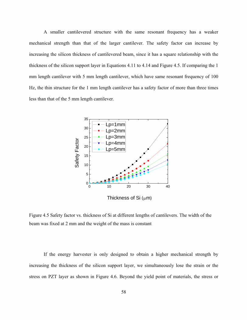
58
A smaller cantilevered structure with the same resonant frequency has a weaker
mechanical strength than that of the larger cantilever. The safety factor can increase by
increasing the silicon thickness of cantilevered beam, since it has a square relationship with the
thickness of the silicon support layer in Equations 4.11 to 4.14 and Figure 4.5. If comparing the 1
mm length cantilever with 5 mm length cantilever, which have same resonant frequency of 100
Hz, the thin structure for the 1 mm length cantilever has a safety factor of more than three times
less than that of the 5 mm length cantilever.
0 10 20 30 400
5
10
15
20
25
30
35
Thickness of Si (μm)
Safe
ty F
acto
r
Lp=1mm Lp=2mm Lp=3mm Lp=4mm Lp=5mm
Figure 4.5 Safety factor vs. thickness of Si at different lengths of cantilevers. The width of the
beam was fixed at 2 mm and the weight of the mass is constant
If the energy harvester is only designed to obtain a higher mechanical strength by
increasing the thickness of the silicon support layer, we simultaneously lose the strain or the
stress on PZT layer as shown in Figure 4.6. Beyond the yield point of materials, the stress or

59
strain dramatically decreases with the thickness of silicon support layer. Since the strain is
directly converted to the output voltage by the piezoelectric PZT layer, the power density
decreases with an increase in the safety factor at a given acceleration force.
5 10 15 20 25 30 35 400.0
5.0
10.0
15.0
20.0
25.0
30.0
35.0
40.0
Thickness of Si (μm)
Stra
in (μ
m)
Lp=1mm Lp=2mm Lp=3mm Lp=4mm Lp=5mm
Figure 4.6 Average strain on PZT vs. thickness of Si at different lengths of cantilevers when the
width of beam was fixed at 2 mm and the weight of mass is constant
Piezoelectric energy harvesters can be designed considering the required specifications of
target environmental conditions using estimation by analytical modeling. The resonant
frequency, safety factor, and output power density are estimated to determine the dimensions of
the cantilever. The results show that the safety factor shows opposite trends compared with the
resonant frequency design and output voltages. The cantilevered energy harvester requires a long
beam, a heavy proof mass, and a thinner Si thickness to match the resonant frequencies of the
energy harvester and ambient vibration source. In the configuration of the cantilevered structure
for low resonant frequency, the safety factor decreased but the output voltages increased. For the
smaller dimension, the mechanical strength is highly decreased while the output voltage

60
converted from the stress increases. The optimization is required to obtain both the mechanical
strength and the output voltages with the resonant frequency in the range of ambient vibration
source.
4.1.4 Analytical output power
The characteristic behavior of piezoelectric energy harvesting can be described by
damping constant and natural frequency. The lumped spring mass system is commonly used to
characterize the dynamic behavior of energy harvesting. Figure 4.7 is simple diagram of a
cantilever beam with a proof mass [2].
Figure 4.7 Equivalent lumped spring mass system
The governing equation of a lumped spring mass system can be expressed by
yMKzzCzM &&&&& −=++ (4.17)

61
where z is net displacement of mass (x – y). The Laplace transform gives the time domain of the
response, z(t), by assuming the external base excitation is sinusoidal as y=Ysin(wt)
( )φω
ωωζ
ωω
ωω
−
⎟⎟⎠
⎞⎜⎜⎝
⎛+
⎟⎟
⎠
⎞
⎜⎜
⎝
⎛⎟⎟⎠
⎞⎜⎜⎝
⎛−
⎟⎟⎠
⎞⎜⎜⎝
⎛
= tgYtz
nn
n sin
21
)(222
2
(4.18)
where ω is a mechanical angular frequency, ωn is a angular resonance. The approximate
transduced power can be obtained from the product of velocity and force, and its maximum value
is under ω = ωn
ζω
4
32
maxnmY
P = (4.19)
At the given input vibration magnitude and mechanical damping, it is necessary to maximize the
mass and minimize the stiffness of the device. Du Toit derived and approximated Equation 2.17,
and gives the simplified displacement (2.20) and output power (2.21) normalized by the input
force (mY) [83] as
( )( )
[ ] ( )( )[ ]23222
2
2 12)21(1
11Ω−Ω+++Ω+−
Ω+=
ααζαζ
α
emm kKmYz
(4.20)
( ) [ ] ( )( )[ ]23222
2
2 12)21(1 Ω−Ω+++Ω+−
Ω=
ααζαζαω
emm
enout
kk
KmYP
(4.21)
pln CRωα =
233
2332
1 kk
ke −=

62
where Rl is load resistance, Cp is capacitance of PZT, k33 is the square root of electromechanical
coupling coefficient, and Ω=ω/ωn.
The output power can be estimated where the piezoelectric coefficient of PZT, d, is 3.2×
10-10 m/V, the dielectric constant of PZT, ε, is 3.36 × 10⁻⁸ F/m, the damping ratio of the
cantilever, ζ, is 0.02, and the coupling coefficient of PZT, k, is 0.44.
4.2 MEMS Fabrication
The following chapter describes the technologies in MEMS fabrication, which led to the
successful fabrication of an energy harvester by integrating piezoelectric thin films into a silicon-
based microsystem. The schematic process flow with three masks for pMEMS cantilevers is
shown in Figure 4.8. A silicon-on-insulator (SOI) wafer was used to give the silicon under layer
a precise and uniform thickness.

63
Figure 4.8 Process flow of piezoelectric MEMS energy harvester using SOI wafer.
The SOI wafer has 20 µm Si device layer and 1 µm buried SiO2 layer. A 500 nm thick
SiO2 was grown on the wafer by thermal CVD, which is the electrical and diffusion buffer layer
during the CSD process. Besides the diffusion and electric barrier, these buffer layers (SiO2 &
Si3N4) can be used to control the residual stress of a multi-layer structure. While other layers are
limited in replacing their materials and changing their thicknesses, the buffer layers have

64
flexibility. It has been reported that SiO2, which was deposited by plasma enhanced chemical
vapor deposition (PECVD), had higher compressive stress and prevented the bending of the
cantilevers by compensating the tensile stress [46]. In this study, the thermal CVD process was
chosen for the buffer layer due to equipment limitations of the facility. Sputter-deposited Pt was
used as a bottom electrode due to its high electrical conductivity and thermal stability at high
temperature. When a multi-layer structure experiences high stress, about 100 MPa, during CSD
heat treatment, a delamination between Pt and SiO2 may occur due to the difference in thermal
expansion of constituent layers [84]. A Ti interfacial layer was used to enhance the adhesion
between Pt and SiO2. After 12 layers of PZT were multicoated to obtain the thickness of about 1
µm, the Pt top electrode was patterned by a lift-off process. The detailed issues of each layer
relating to the fabrication of pMEMS structure are summarized in Table 4.2.
Table 4.2 Specification and issues of individual layer in fabricating pMEMS energy harvesters
Layers Materials
(thickness) / dep. Tech.
Functions Issues Solution approach
Top electrode
Pt (120 nm) /
Sputter ⋅Electrical contact
⋅ Ohmic contact ⋅ Strong adhesion during MEMS process (PR stress)
⋅Deposition process control
Piezo-electric layer
PZT (1 μm) / Sol-gel
⋅ Transfer strain energy to electrical energy
⋅ Orientation ⋅ Stress
⋅ Control substrate orientation with piezoelectric mode
Bottom electrode
Pt (120 nm) / sputter
⋅ Electric contact ⋅ Control orientation of piez. Layer
⋅ High stress is loaded during PZT annealing
delamination
⋅ Adhesion layer ⋅ Orientation control by sputter parameters

65
Adhesion layer
Ti, Cr, or Ta (10 nm) / sputter
⋅ additional adhesion between films
⋅ Diffusion through the GB ⋅ Degradation of PZT layer
⋅ Limited source Very thin
film
Membrane
SiO2 (500 nm) /
Thermal CVD ⋅ Mechanical support ⋅ Buffer layer of diffusion ⋅ Etching stop
⋅ Stress after cantilever release ⋅ Stress design
Si3N4 (300nm) / LPCVD
Si (0~20 μm) /
CZ
⋅ Mechanical support ⋅ Stress compensation
⋅ Uniformity ⋅ Thickness control during etching process
⋅ Process (DRIE) engineering ⋅ Effective etching stop (SOI wafer)
After piezoelectric thin film is successfully deposited in wafer scale, the cantilever should
be built up considering the precise dimension control and damages to the piezoelectric transducer
layer. RIE is one of the dry etching methods that can provide cleanness, precise etching control,
low chemical damage, an ability for mass production, and fast etching rate with physical and
chemical reactions. SF6 is more innoxious and shows a moderate etching rate on each film of
pMEMS, although chlorinated gas has a faster etching rate on PZT due to highly volatility metal
chloride. Process parameters are optimized by considering the etching rate, damages, and
selectivity to the photoresist mask that serves as a protective layer.
4.2.1 Lithography and mask for DRIE
A lithography process was used for patterning the top electrode and etching mask for the RIE
system. The clearly defined vertical profile of the patterned photoresist is required for a precise
66
pattern of a Pt top electrode after lift off and etching profile at the edge of pattern for the etching
mask.
Since a platinum top electrode was deposited by a sputter system, the incident angle of the
accelerated atoms during deposition is not normal to the substrate. The angle of the accelerated
atoms is created due to the collision through the pathway of atoms from target to substrate. If the
cathode is not normal to the substrate in the sputter system, the angular deposition is more
serious. As deposited film on the sidewall of photoresist gets thicker, it is hard to be removed by
the lift-off process. If the lift-off process is performed by perforce, the top electrode can be torn
away or remain as a scrap of sidewall film that induces the electric shortage of a piezoelectric
cantilever corresponding to 1 µm thin PZT layer.
A vertical or acute side wall angle of patterned photoresist improves the successful patterning
of top electrode without any damage or electric shortage. Their sidewall has been shadowed with
less area exposed to the cathode, and the probability of deposition of film on the sidewall is
lessened. Negative photoresist (nLof 5014) was used to obtain the vertical or acute angle. While
a positive photoresist easily creates an obtuse angle due to over exposure or development, the
negative photoresist can make an acute angle due to its inverse patterning. Figure 4.9 shows the
vertical profile of the sidewall using negative photoresist. The delamination at the edge seems to
have happened during cracking of the sample to see the cross section view.

67
Figure 4.9 Edge of negative photoresist pattering.
Various polymer and metal film masks are used in the DRIE system for patterning. Metal
masks have a high resistivity to the DRIE etching mechanisms, which have both chemical
reactions and physical ion bombardment of ionized gas. In spite of the advantages of metal
masks, the metal mask cause damage to PZT by creating internal stress due to the deposition of
the metal mask. After removing the Al mask by an acid solution of phosphoric acid and acetic
acid (PAE) etchant, damage on the top electrode was evident, as shown in Figure 4. 10. The top
electrode was completely peeled off, and the bottom Pt was seen at the edge of cantilever where
the PZT was peeled off. Conductive Pt was indicated by a brighter image than that of PZT layer
in the SEM. The cracked Pt shows that internal stress existed, and the damages at the edge of
cantilever seem to be caused from the internal stress or penetrating of etchant between PZT and
bottom Pt.
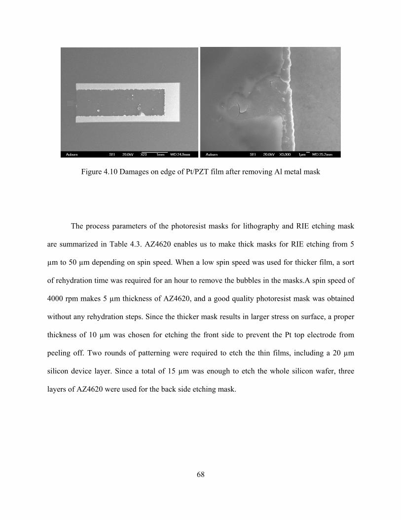
68
Figure 4.10 Damages on edge of Pt/PZT film after removing Al metal mask
The process parameters of the photoresist masks for lithography and RIE etching mask
are summarized in Table 4.3. AZ4620 enables us to make thick masks for RIE etching from 5
µm to 50 µm depending on spin speed. When a low spin speed was used for thicker film, a sort
of rehydration time was required for an hour to remove the bubbles in the masks.A spin speed of
4000 rpm makes 5 µm thickness of AZ4620, and a good quality photoresist mask was obtained
without any rehydration steps. Since the thicker mask results in larger stress on surface, a proper
thickness of 10 µm was chosen for etching the front side to prevent the Pt top electrode from
peeling off. Two rounds of patterning were required to etch the thin films, including a 20 µm
silicon device layer. Since a total of 15 µm was enough to etch the whole silicon wafer, three
layers of AZ4620 were used for the back side etching mask.

69
Table 4.3 Parameters of lithography processes
Resist
Thickness
per layer
(µm)
Spin
speed
(rpm)
Prebake
(ºC/min)
Exposure
time
(sec)
Post bake
(ºC/ min)
Developing
(min/developer)
nLOF 2031 2.5 3500 110/1 4.5 110/1 0.8 / AZ300
AZ 4620 5 4000 105/3 30 N/A 1 / A400K(1:3)
4.2.2 Silicon bulk micromachining (Advanced Silicon Etcher)
Silicon bulk micromachining has been widely used for micro sensors and actuators.
Etching silicon is categorized as the medium of etchant by wet and dry etching. Silicon etching
from the wet phase mostly uses the mixture (HNA) of hydrofluoric acid (HF), nitric acid (HNO3)
and acetic acid (CH3COOH), Tetramethyl-ammonium hydroxide (TMAH), or Alkali-OH (KOH)
chemicals. While HNA shows an isotropic etching profile in three dimensions, others have
anisotropic etching profiles depending on the crystallographic orientation. The dry etching for
silicon is usually conducted using a vapor phase etchant or plasma with etchant gas. XeF2 is
mostly used for the vapor phase etchant of silicon, and its reaction is 2XeF2 + Si 2Xe(g) +
SiF4(g). Plasma etching using reactive gas is the favorable method in micromachining the device
due to fast etching rates and available process variables to control the etching profile. This study
used plasma etching for bulk micromachining due to its excellent shaping ability, and detailed
information is given in the next section.
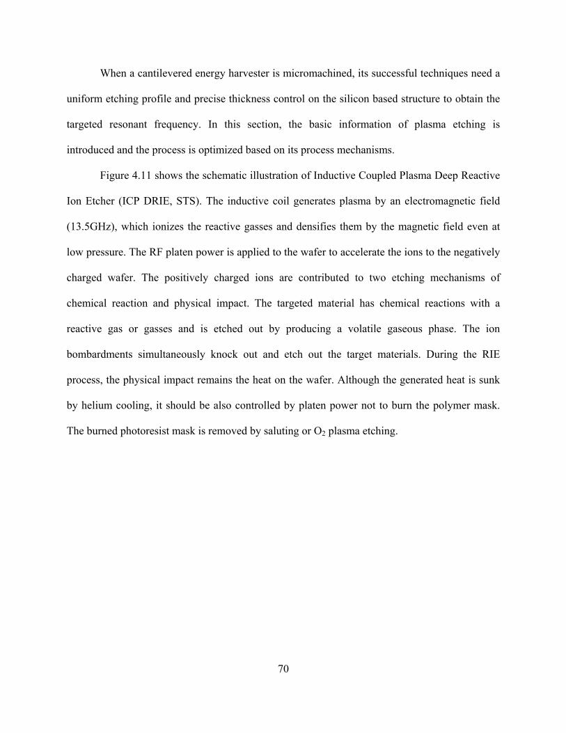
70
When a cantilevered energy harvester is micromachined, its successful techniques need a
uniform etching profile and precise thickness control on the silicon based structure to obtain the
targeted resonant frequency. In this section, the basic information of plasma etching is
introduced and the process is optimized based on its process mechanisms.
Figure 4.11 shows the schematic illustration of Inductive Coupled Plasma Deep Reactive
Ion Etcher (ICP DRIE, STS). The inductive coil generates plasma by an electromagnetic field
(13.5GHz), which ionizes the reactive gasses and densifies them by the magnetic field even at
low pressure. The RF platen power is applied to the wafer to accelerate the ions to the negatively
charged wafer. The positively charged ions are contributed to two etching mechanisms of
chemical reaction and physical impact. The targeted material has chemical reactions with a
reactive gas or gasses and is etched out by producing a volatile gaseous phase. The ion
bombardments simultaneously knock out and etch out the target materials. During the RIE
process, the physical impact remains the heat on the wafer. Although the generated heat is sunk
by helium cooling, it should be also controlled by platen power not to burn the polymer mask.
The burned photoresist mask is removed by saluting or O2 plasma etching.

71
Figure 4.11 The illustration of DRIE
The process condition was systematically investigated by examining the variables and
their effects as summarized in Table 4.4.
Table 4.4 The process variables and their effects on etching
Parameters Effectiveness
Coil power Plasma density
Platen power Acceleration of ions
Gas flow and Chamber pressure
Plasma density Turbulence
Gas type Chemical reaction
Etching and passivation cycle Etching rate and surface profile

72
SF6 and O2 gasses were used in the etching process. The glow discharge in plasma
generates free radicals of SxF’y and O’:
SF6 + e- SxFy + SxF’y + F’ + 2e-
O2 + e- O+ + O’ + 2e-
while the free oxygen radicals create the passivation layer of an oxide film, and the fluorine is
desorbed after the reaction with Si as a gas of SiF:
Si + 4F’ SiF4 (g)
To obtain a vertical etching profile, silicon etching is performed by repeating passivation
using C4F8 for 7 seconds and etching using SF6 and O2 for 13 seconds as shown in Figure 4.12.
After etching, the passivation layer is covered on all surfaces and walls. This etching effectively
removes the surface due to the normal direction of accelerated ions, but not on the wall. This
cyclic process makes the vertical angle of the side wall, and the ratio between etching and
passivation detemines the profile of the sidewall in microscopic and macroscopic forms. For
example, the short cycle induces the smooth surface in the microscopic form and the very
vertical sidewall in macroscopic form. The short cycle also results in a slow etching rate. The
optimal cycle is required to balance the profile of the sidewall and etching rate.

73
Figure 4.12 Cyclic etching and passivation of ASE process
Since the uniform etching profile mostly induces the slow etching rate, the optimized
condition was investigated considering a moderate etching rate and uniformity. Plasma density,
platen power of acceleration, chamber pressure, cycle of etching, and passivation were
considered, and the recipe was built in Table 4.5.
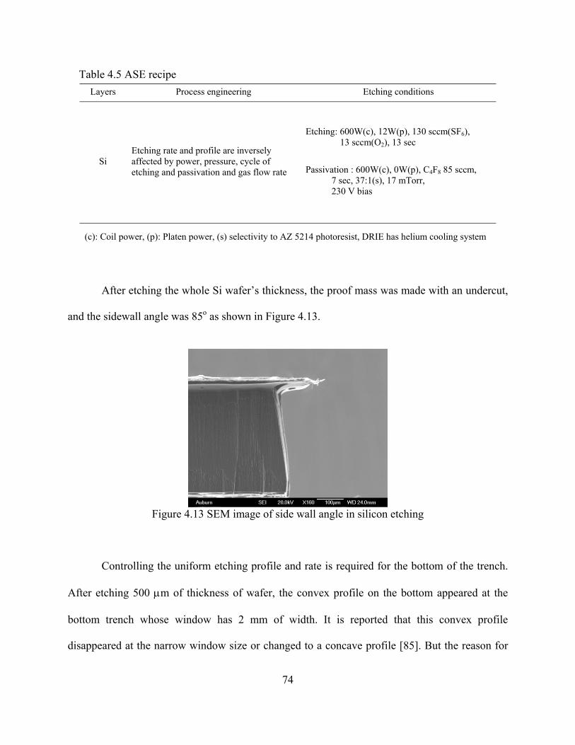
74
Table 4.5 ASE recipe Layers Process engineering Etching conditions
Si Etching rate and profile are inversely affected by power, pressure, cycle of etching and passivation and gas flow rate
Etching: 600W(c), 12W(p), 130 sccm(SF6), 13 sccm(O2), 13 sec
Passivation : 600W(c), 0W(p), C4F8 85 sccm, 7 sec, 37:1(s), 17 mTorr, 230 V bias
(c): Coil power, (p): Platen power, (s) selectivity to AZ 5214 photoresist, DRIE has helium cooling system
After etching the whole Si wafer’s thickness, the proof mass was made with an undercut,
and the sidewall angle was 85o as shown in Figure 4.13.
Figure 4.13 SEM image of side wall angle in silicon etching
Controlling the uniform etching profile and rate is required for the bottom of the trench.
After etching 500 μm of thickness of wafer, the convex profile on the bottom appeared at the
bottom trench whose window has 2 mm of width. It is reported that this convex profile
disappeared at the narrow window size or changed to a concave profile [85]. But the reason for

75
this phenomenon is not well understood yet. It is suggested that the plasma density in the deep
trench is not uniform so that the profile shows a difference as the window size varies. The
chamber pressure was regulated to control the turbulence by the gas flow rate. The uniform depth
profile was improved from 5% to 3% during the etching of the thickness (~500 μm) of the
silicon wafer when using lower pressure conditions at the same gas flow. The uniformity was
near a 15 μm thickness variation and was created during etching out 500 μm of silicon wafer by
reducing the chamber pressure from 36 mTorr to 17 mTorr at the same gas flow, as shown in
Figure 5.3. The uniformity was obtained by measuring the thickness of the cantilevers by an
SEM image at the anchor, middle, and end tip positions.
The different sizes of the window made different etching rates during silicon etching, and
this is called the lag effect [86, 87]. Although the widely opened areas have been etched out and
the cantilever has been released, the narrow window beside the proof mass still remained, as
shown in Figure 4.14. These results from etching rates that are different from the window sizes.
The excess etching time to release the cantilever under the lag effect resulted in thinner
cantilever beams whose window size is larger than that expected. Since the lag effect can be
hardly solved by changing the etching conditions, it should be considered during designing the
masks. After giving the same space as that between the window and the cantilever head, the lag
disappeared.
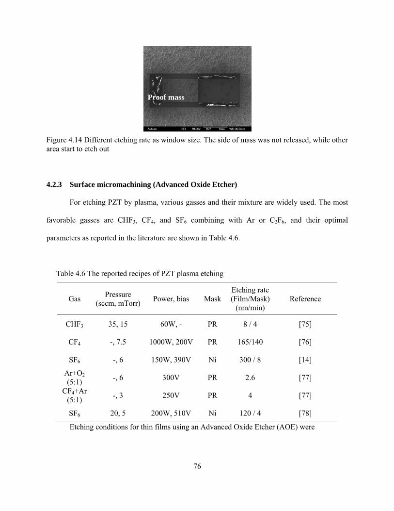
76
Figure 4.14 Different etching rate as window size. The side of mass was not released, while other area start to etch out 4.2.3 Surface micromachining (Advanced Oxide Etcher)
For etching PZT by plasma, various gasses and their mixture are widely used. The most
favorable gasses are CHF3, CF4, and SF6 combining with Ar or C2F6, and their optimal
parameters as reported in the literature are shown in Table 4.6.
Table 4.6 The reported recipes of PZT plasma etching
Gas Pressure (sccm, mTorr) Power, bias Mask
Etching rate (Film/Mask)
(nm/min) Reference
CHF3 35, 15 60W, - PR 8 / 4 [75]
CF4 -, 7.5 1000W, 200V PR 165/140 [76]
SF6 -, 6 150W, 390V Ni 300 / 8 [14]
Ar+O2 (5:1) -, 6 300V PR 2.6 [77]
CF4+Ar (5:1) -, 3 250V PR 4 [77]
SF6 20, 5 200W, 510V Ni 120 / 4 [78]
Etching conditions for thin films using an Advanced Oxide Etcher (AOE) were
Proof mass

77
investigated using SF6 gas by considering the etching rate, etching profile, and selectivity
against photoresist mask. A literature survey showed that SF6 gas can show a moderate etching
rate without leaving remaining residues on the surface after a reaction. When the reactive gas is
chosen, the process parameters should be optimized not to make damages on the films due to the
physical energy of ion bombardments with considering etching rate.
Figure 4.15 Cracks were created on PZT due to strong ion bombardment
Energetic ion bombardment induced from high platen power would result in burning
photoresist that is hard to remove or decreasing the selectivity of the photoresist mask. Since the
charges concentrate on the edge of the photoresist mask, the mask shows a faster etching rate at
the outside of the pattern. The excess etching rate using a high platen power etched out
photoresist mask from opened window and damaged the PZT films around the squire window, as
shown in Figure 4.15. Moreover, energetic ion bombardments can directly damage the PZT film
[ ]. After etching the PZT using a high platen power of 300W, cracks were found on the PZT
film and theycontinued to the area where the PZT film was already etched out in Figure 4.15.
Since these cracks were found to be distributed around the other square etching windows of the
same sample, it seems that the cracks were initiated from the etched region and were caused by

78
RIE etching. When the platen power was reduced to 200W and the chamber pressure was
increased to provide sufficient reactive gas for etching, the etching rate increased 2.5 times but
the cracks were still found with the fast etching rate. The power, chamber pressure, and gas flow
were optimized with 70 nm/min of moderate etching rate and without damage on the films.
The process parameters for AOE were investigated and optimized for the moderate
etching rate and to prevent damage on the PZT films as shown in Table 4.7.
Table 4.7 Investigation of process parameters of AOE system for etching PZT thin film
Coil power
Platen power
Pressure (mTorr)
Gas flow (sccm)
Bias (V)
Etching rate (nm/min) Comments
800 300 5 20 250 40 -Moderate etching rate -Crack on PZT film
600 200 30 50 270 100 -Fast etching rate -Low selectivity -Little crack
600 150 20 30 230 70 - Moderate etching rate - No damage
600 100 5 20 90 10 - Slow etching rate
Photoresist is selected as the mask for the DRIE process due to its clean patterning and
least amount of created stress as compared to the metallic films that can induce device failure
during fabrication due to their high internal stress. SiO2 and thin metal layers (Pt/Ti) were also
effectively etched out by the same recipe for PZT etching, as seen in Table 4.8. The high

79
momentum of ion bombardment resulted in an acceptable etching rate for the very thin
Pt/Ti/SiO2 films.
PZT/Pt/Ti/SiO2 layer could be vertically etched after 25 min of etching time, and its cross
section view is shown in Figure 4.16. The detailed recipe for AOE is shown in Table 4.8.
Figure 4.16 SEM image of etched PZT film surface in cross section view
Table 4.8 AOE recipe
Layers Growth Thickness Selectivity Etching rate Etching conditions
SiO2 Wet oxidation 500 nm 1:1(s) 90 nm/min
600W(c), 150W(p), 30sccm(Ss
Ti interlayer
Magnetron sputtering 10 nm
Pt electrode
Magnetron sputtering 120 nm 1:30(s) 23 nm/min
PZT 52/48 Sol-gel deposition 1 µm 1:10(s) 70 nm/min
(c): Coil power, (p): Platen power, (s) selectivity to AZ 5214 photoresist, DRIE has helium cooling system

80
4.2.4 Designing masks based on optimized pMEMS process
For successful fabrication of piezoelectric-based MEMS devices, two processes should be
optimized. First, the integration of PZT on the Si wafer is a key issue of piezoelectric-based
sensors, actuators, and energy harvesters. Although PZT has very high piezoelectric properties in
bulk scale, the degradation of its properties might occur in film scale. The other is that the design
and fabrication process were optimized for the successful energy harvester. A non-uniform
etching profile during micromachining is a major issue in fabricating pMEMS energy harvesters.
The micromachining might result in the degradation of piezoelectric properties, the shift of
resonant frequency from the targeted one, and a decrease in the mechanical strength due to stress
concentration on the weak part during resonating. This section shows how the designing masks
have been developed considering the optimized film deposition and micromachining. The masks
were designed by a LASI software tool.
The first mask in Figure 4.17 was designed by following concepts and resulted in the
following:
1. The rectangular cantilever and bridge structures were included in this mask. The bridge
structure withstood a very high acceleration, but the output signals were very low. The
detail evaluation of the bridge structure do not apply in this study.
2. The main objectives of the first mask were to optimize the fabrication process and verify
the resonant frequency. After etching out the whole Si layer, the Pt/PZT/Pt/Ti/SiO2 multi
layer was seriously bent up due to internal stress as predicted. The bending curvature was
so large over 90 degrees that the cantilever structure almost failed without the silicon

81
substrate. The devices were also easily broken down during carriage.
3. Besides compensating for the internal stress by applying thin oxide films and/or
controlling their stress by a growth method, the remaining Si under layer was chosen due
to easy fabrication and because it suppliess high mechanical strength. The bending
configurations of the cantilever structure as Si thickness will be introduced in Chapter 5.
The thickness of the Si layer could be controlled by adjusting the etching parameters of a
DRIE Si etching system.
4. The conventional lag effect was found during releasing cantilever by Si etching. The
different window size induced the non-uniform etching rate. Since the lag effect required
additional etching time to complete releasing of the cantilevers, it was hard to control the
accurate Si thickness only by etching time.
After examining the feasibility of the fabrication process using the first mask, the second
mask was designed considering the Si membrane.
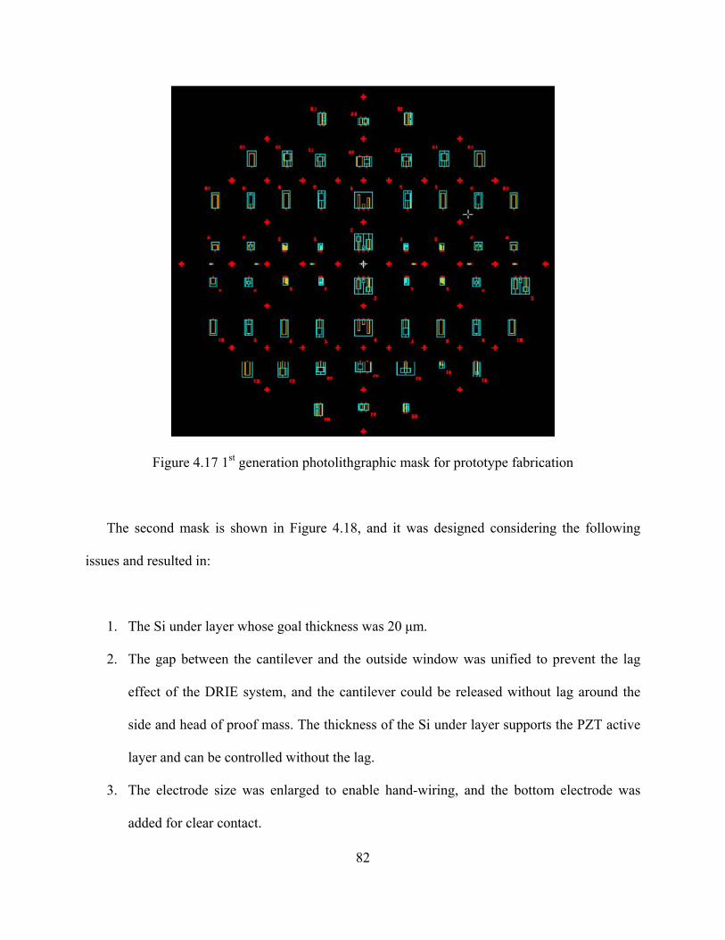
82
Figure 4.17 1st generation photolithgraphic mask for prototype fabrication
The second mask is shown in Figure 4.18, and it was designed considering the following
issues and resulted in:
1. The Si under layer whose goal thickness was 20 μm.
2. The gap between the cantilever and the outside window was unified to prevent the lag
effect of the DRIE system, and the cantilever could be released without lag around the
side and head of proof mass. The thickness of the Si under layer supports the PZT active
layer and can be controlled without the lag.
3. The electrode size was enlarged to enable hand-wiring, and the bottom electrode was
added for clear contact.

83
4. The top electrode size was reduced comparing PZT layer to prevent possible electric
shortage between the top and bottom Pt electrode after fabricating. The electric shortage
could be prevented by reducing the size of the top electrode by 15 µm.
5. The prototype of the cantilever array was tested. The non-uniformity of the device
dimensions in wafer scale might exist from the center to edge or right to left due to the
special density of plasma and turbulence of reactive gases. The discrepancy of resonant
frequency of each cantilever due to non-uniform etching rate will be introduced in
Chapter 5.
6. The non-uniform etching profiles on the side wall of the proof mass and the surface of Si
under layer were found by SEM analysis. Such a non-uniform etching profiles induced
the shift of resonant frequency from calculated values. The process was optimized to
improve etching profiles, but the RIE process has a limitation to maintain the sufficient
etching rate. The etching top layer was required for the uniform profile to obtain a goal
resonant frequency.
7. The cantilevers have resonant frequencies under 100 Hz. The dimensions of the
cantilever were varied to examine the width, length, and weight of the proof mass. The
detailed dimensions are denoted in Table 4.9 and Table 4.10. The notations in the Tables
are based on Figure 4.2.

84
Figure 4.18 2nd generation photolithgraphic mask for prototype fabrication

85
Table 4.9 Dimension and resonant frequency of single cantilever in 2nd mask Wp Lp L Wm Hm Lm Fr #
500
2100 4100
2000 500 2000
99 1
2600 4600 83 2
3100 5100 71 3
3400 4900 1500 500 1500
101 4
4100 5600 82 5
2500 4500 1500 500 2000
99 6
3100 5100 82 7
1000
3200 5200 2000 500 2000
98 8
3800 5800 83 9
2000 4500 2500 500 2500
97 10
2500 5000 83 11
1600 4600 2000 500 3000
96 12
2100 5100 82 13
2000 5000 1500 500 3000
97 14
2600 5600 82 15
2600 5600 1000 500 3000
100 16
3300 6300 83 17
Table 4.10 Dimension and resonant frequency of cantilever array in 2nd mask Wp Lp L Wm Hm Lm Fr #
500 2100 4100 2000 500 2000 99 1
1000 2500 5000 2500 500 2500 83 11

86
The third mask is shown in Figure 4.19, and it was designed and resulted as follows:
1. The mask was designed to test various shapes of cantilever structures such as circularly
filleted notch andtrapezoid.
2. A SOI wafer with 20 µm Si device layer was used for a uniform Si under layer, and to
verify the modeling of the resonant frequency.
3. The design radically located the devices from the center of the wafer to investigate the
uniform etching rate in the wafer scale. The highly dense location of the cantielver was
enabled when using the dicing line of the silicon etching mask, and a high product yield
might be possible. The failure during the dicing device also might also be prevented
Figure 4.19 3rd generation photolithgraphic mask for prototype fabrication

87
The cantilever array was tested in parallel connection for high current yield. The cantilever array
was located in radical for uniform etching. These prototypes were relatively large scale to
observe the feasibility of the cantilever array. The fabricated prototypes are pictured in Figure
4.20, and the mask is shown in Figure 4.21. The SiO2 layer can be seen on the backside of the
cantilever, and the reflected color shows the non-uniform thickness of the SiO2 after ASE
etching. The different between the maximum and minimum thickness is very small, under 300
nm, when inspecting the color chart of SiO2.
Figure 4.20 prototype cantilever array

88
Figure 4.21 photolithgraphic mask for cantilever array prototype
The fourth mask (Figure 4.21) was designed to study the modeling of resonant frequency,
interdigitated electrode, and serially connected array, mechanical strength, and geometry stress
on the cantilever. The detailed dimensions as a function of device are denoted in Table 4.11.

89
Figure 4.22 4th generation photolithgraphic mask for prototype fabrication
Table 4.11 Dimension of devices on 4th mask
Comments Cal fr (Hz)
Safety factor Lp (m) Wp (m) Wm (m) Lm(m)
Array (S & P) 125.58 7.90 4.00E-03 2.00E-03 2.00E-03 3.00E-03
d33 125.58 7.90 4.00E-03 2.00E-03 2.00E-03 3.00E-03
Geometry stress test 125.58 7.90 4.00E-03 2.00E-03 2.00E-03 3.00E-03
Width check
125.58 7.90 4.00E-03 2.00E-03 2.00E-03 3.00E-03
125.58 7.90 4.00E-03 3.00E-03 3.00E-03 3.00E-03
125.58 7.90 4.00E-03 4.00E-03 4.00E-03 3.00E-03
125.58 7.90 4.00E-03 5.00E-03 5.00E-03 3.00E-03

90
Frequency check
169.98 9.72 3.00E-03 2.00E-03 2.00E-03 3.00E-03
145.01 8.72 3.50E-03 2.00E-03 2.00E-03 3.00E-03
125.58 7.90 4.00E-03 2.00E-03 2.00E-03 3.00E-03
110.12 7.22 4.50E-03 2.00E-03 2.00E-03 3.00E-03
97.57 6.64 5.00E-03 2.00E-03 2.00E-03 3.00E-03
87.23 6.14 5.50E-03 2.00E-03 2.00E-03 3.00E-03
Length/Width Ratio
125.58 7.90 4.00E-03 2.00E-03 2.00E-03 3.00E-03
125.45 6.61 3.52E-03 1.50E-03 2.00E-03 3.00E-03
125.86 5.37 3.10E-03 1.00E-03 2.00E-03 3.00E-03
125.59 3.42 2.17E-03 5.00E-04 2.00E-03 3.00E-03
The fifth mask in Figure 4.23 was designed as follows:
1. To investgate the size effect, poling effect, aging and fatigue effect, and geometry stress
test as cantilever shapes.
2. The trapezoid might alter the stress distribution and increase the output power. The
trapezoidal cantilever in the third mask showed no improvement of output power. The
stress distribution will be examined by three different electrodes located on the near
anchor, middle of cantilever, and near proof mass. The output signals from three
electrodes will be used to analyze stress distribution. Signals from the rectangular
cantilever with the same electrode configuration will be compared and anlyzed.

91
Figure 4.23 5th generation photolithgraphic mask for prototype fabrication

92
CHAPTER 5 DEVICE CHARACTERIZATION AND ANALYSIS
5.1 Experimental setup for characterization
The output signals from the energy harvester mounted on an electromagnetic shaker
(Labworks In., ET-132-203) were measured by an oscilloscope (Tektronix, TDS3014B). The
sinusoidal vibration of the shaker was controlled by an amplified source from an external
function generator (Agilent 33220A). The generated vibration was simultaneously monitored by
an accelerometer (PCB piezoelectronics Inc., 352C65) whose signal was monitored by the
oscilloscope. The output voltage from the device was measured across the resistor, which could
be regulated to find the optimal resistance load. The peak-to-peak output power was used to
calculate the power, and the recorded output wave was used for the AC-DC rectifier. The
schematic experimental setup is shown in Figure 5.1.
Figure 5.1 Schematic of experimental setup for energy harvester

93
5.2 Performance of single cantilever
The characterizations of the energy harvester are categorized to investigate PZT film
properties, resonant frequency, and output signal during resonance conditions. The results of film
properties have already been discussed in Chapter 4. The PZT films had similar polarization
values (Pr and Pmax) before and after been fabrication process. A minor distortion of been
hysteresis loop occurred, and it seemed to be caused from the stress of the released cantilevers
after completing the fabrication and/or defects due to the diffusion of substrate materials. The
resonant frequency was measured by an impedance analyzer and the maximum output voltage
was tracked via an oscilloscope. The power was calculated from the output voltage by Ohm’s
law. To rectify the AC generated from the energy harvester to DC for storage, the Vrms value was
used for calculations. In this chapter, the resonant frequency of the devices and output signal will
be analyzed and discussed.
5.2.1 Device on silicon wafer
The internal stress makes the cantilever bend upward due to the net tensile stress between
the Pt/PZT/Pt/SiO2 layers. Although the net stress can be controlled by the proper material
selection of a buffer layer (SiO2 or SiNx) with a different deposition method, a thicker Si layer
was chosen to prevent bending as well as to enhance the mechanical strength of the device.
Without a Si support layer, the Pt/PZT/Pt/SiO2 was seriously bendt and failed, as shown in
Figure 5.2 (c). The internal stress was experimentally examined as the thickness of the Si under
layer. At 100 µm of Si thickness, the cantilever showed no bending due to stiff support in Figure

94
5.2 (a). The bending of the cantilever was not found up to 20 µm of Si thickness, but it started to
bend upward due to tensile residual stress from 10 µm of Si thickness.
Figure 5.2 Cantilevers have different average thicknesses on Si under layer as (a) 100 μm, (b) 20 μm, and (c) 10 μm (cantilever was bend due to internal stress).
The resonant frequency is sensitive to dimensions, especially the thickness. The first
attempt was controlling the Si thickness by a DRIE etching process. The current recipe etches the

95
silicon with about 1 µm per 1 cycle (20sec) of etching rate. A 20 µm Si under layer was expected
by the DRIE etching process. The process time-based thickness control was reasonablly capable
when the silicon support layer remained at an average of 27 µm of silicon thickness during 550
µm etching. The problem was very poor uniformity of the cantilever, as shown in Figure 5.2.
The Si layer showed a convex profile with a relative thinner region on the near anchor and proof
mass. It is not clearly understood why the convex profile occurs at the wide window size of the
pattern, while the narrow window shows a concave profile. It seems that the bias in the trench is
locally different [88]. It was also suggested that abnormal gas conditions in the deep trench with
a wide window made non-uniform etching configuration geometrically [89].
(a)
(b)

96
(c)
(d) Figure 5.3 Geometric graph of cantilever’s thickness: (a) Sampled cantilevers and their location, (b) Thickness at the joint on proof mass, (c) Thickness at the middle of cantilever, (d) Thickness at the joint on anchor
Based on a literature survey and experiments, the uniformity can be controlled to set a
short etching and passivation cycle, low power, and high chamber pressure [88-90]. But their
adjustments by optimizing process conditions lead to a very slow etching rate. The uniformity
was investigated in wafer scale from the center to the edge. Three positions, near anchor, middle,
and end tip, of the cantilevers were measured for their thickness. The uniformity of the cantilever
beam varies according to the window size, but does not depend on the location in the wafer
scale. On the contrary, the etching rate varies according to the location in the wafer. The center
of the wafer generally shows a higher etching rate compared to that of the edge. Since the
calculated resonant frequency assumes a uniform beam thickness, the measured values show a
large deviation. The measured resonant frequencies were in a range between resonant
frequencies calculated using maximum and minimum thickness. Since the piezoelectric energy
harvester needs precise frequency matching with the target application, an unexpected shift of
resonant frequency caused from non-uniform thickness led to functional failure.

97
211
200 210 220
-87.30
-87.25
-87.20
-87.15
-87.10
-87.05
-87.00
Phase Impedence
Frequency (Hz)
Phas
e A
ngle
(o )
6000
6250
6500
6750
7000
Impedence (Ω
)
Figure 5.4 The resonant frequency of cantilever fabricated on Si wafer
A cantilever that has 5mm(L) x 1mm(W) of beam dimensions and 2.5mm(L) x
2.5mm(W) of mass dimensions has 162 Hz of calculated resonant frequency. The measured
resonant frequency was 211 Hz as shown in Figure 5.4. The cantilever has 15 µm, 35 µm, and 20
µm of thickness near the anchor, middle, and end tip. A 211 Hz resonant frequency estimates 24
µm of uniform silicon thickness. A 1 µm thickness deviation makes a shift of resonant frequency
of about 10 Hz as shown in Figure 5.5.

98
15.0 20.0 25.0 30.0 35.0
100
150
200
250
300
350
400
Res
onan
t fre
quen
cy (H
z)
Thickness of Si
Figure 5.5 Resonant frequency is very sensitive to the thickness of the beam
Figure 5.6 shows the output peak voltage and calculated output power by Ohm’s law at
different resistance loads. When the maximum power is attained at 6.5 kΩ of optimal resistance
load, the device had 147 mV of peak voltage and 0.42 µW under 0.75 g acceleration force. The
power density is 130 µW/cm3 that is very low when comparing it with the other prototypes
shown in Table 2.5. The peak voltage is too small for the rectifier circuit to diminish the current.
The device was broken during resonating under 1 g of acceleration force. All characterized
values are shown in Table 5.1.

99
10 20 30 40 50 600.0
0.1
0.2
0.3
0.4
0.5
Pav
e (μW
)
Rload (kΩ)
0.25G 0.5G 0.75G 1G
(a)
0 10 20 30 40 50 600
40
80
120
160
200
240
#11
Out
put V
olta
ge (m
V)
Resistance (kΩ)
0.25 G 0.5 G 0.75 G 1 G
(b)
Figure 5.6 (a) Output peak voltage, and (b) power from single cantilever on Si

100
Table 5.1 Characteristic of energy harvester on Si wafer
Resonant frequency (Hz) Optimal
resistance (kΩ)
Optimal peak
voltage (mV)
Optimal peak
power (µW)
Safety factor
Volume (mm3)
Cal. Mea.
162 211 6.5 147 0.42 0.75 3.225
The device, fabricated on a silicon wafer, induced low power and mechanical strength,
and a large deviation of resonant frequency. A hypothesis will be that the insufficient
performance was caused by non-uniform silicon layers, as shown in Figure 5.7. During
resonating, the stress was concentrated on the thinner part near the anchor. Since the amount of
polarization is limited over large strain due to limitations of switching the domain, the low output
power seems to be contributed from the restricted strain and area. While a resonating cantilever
under a mechanical load induces nonlinear strain on the surface of the cantilever structure, the
wide distribution of strain on the cantilever beam is preferred for energy harvesters. The low
mechanical strength is also caused from the concentrated stress, and it made failure on the red
circled zone, which generally has the highest strain. The frequency tuning by dimension control
seems hard with silicon wafers, even if optimized etching conditions are used.

101
Figure 5.7 Concave etching profile after silicon etching
5.2.2 Device on Silicon-On-Insulator (SOI) wafer
To obtain a uniform profile of the silicon under layer, an SOI wafer was used. The SOI
wafer had 20 µm of silicon device layer and 1 µm of buried oxide (SiO2). The thickness of the
silicon device layer was chosen to prevent bending of the cantilever based on the previous
experiments. The uniformity of the device layer was less than 0.1 µm, which may induce about
0.5 Hz shift from the estimation considering 0.05 µm of average value. The device has
dimensions of 4 mm x 2 mm x 0.021 mm for the beam and 3 mm x2 mm x 0.5 mm for the proof
mass, and its total volume, including beam and mass, are shown in Table 5.2.
The uniformity of the silicon under layer is estimated at less than 500 nm based on the
reflectance index of SiO2. The buried SiO2 can be removed by wet etching when the front side of
the wafer is passivated by photoresist after releasing the cantilever from the backside. It was not
removed in this study to prevent creating an initial notch, which may result in early failure of the
structure during resonating. The buried oxide thin layer was not considered on modeling of
resonant frequency.
The resonant frequency was measured by tracking the maximum voltage during sweeping

102
the frequency in 0.1 Hz intervals. The difference from the calculated valued was just 1%. To
verify the analytical modeling of the resonant frequency, four other cantilevers in Figure 5.8 (a),
which have different lengths, were sampled, and their resonant frequencies were measured as
shown in Figure 5.8 (b). The modeling of the resonant frequency has good agreement with the
experimental results at low frequency ranges.
3.0 3.5 4.0 4.5 5.0 5.5 6.0
80
100
120
140
160
180
Res
onan
t fre
quen
cy (H
z)
Length of cantilever (mm)
Calculated values Measured value
(b)
Figure 5.8 Comparison between resonant frequencies of estimated and measured values
The output peak voltage and power were plotted in Figure 5.9. When PEH was poled at
120 ºC under 20V for 10 minute, the maximum power was obtained as 6.72 µW at the 11 kΩ of

103
optimal resistance load and 0.5 g of acceleration. This energy harvester fabricated on SOI wafer
increased the power density as 2144 µW/cm3, which is 15 times higher than that of the harvester
fabricated on the Si wafer. The output voltage also increased and generated 0.77 V at optimal
conditions, which may be over the threshold voltage of circuits. The characterized values are
summarized in Table 5.2.
0 5 10 15 20 25 30 35 400
200
400
600
800
1000
1200
Vpk
-pk (m
V)
Resistive load (kΩ)
0
2
4
6
Pow
er (μW)
Figure 5.9 Output peak voltage and power of device fabricated on SOI wafer
Table 5.2 Characteristics of energy harvester fabricated on SOI wafer
Resonant frequency (Hz) Optimal
resistance (kΩ)
Optimal peak
voltage (mV)
Optimal peak
power (µW)
Safety factor
Volume (mm3)
Cal. Mea.
138.61 140.3 11 769 6.72 8.1 3.294

104
5.3 Performance of cantilever array
5.3.1 Device on Si and SOI wafer
The cantilever array consisted of 10 cantilevers fabricated to increase output power via
increasing voltage or current. The resonant frequencies of cantilever arrays were evaluated as
shown in Figure 5.10. The array energy harvesters were separately fabricated on Si and SOI
wafers. Several peaks of resonant frequencies of each cantilever in the array were shown in the
80Hz range from 169Hz to 233Hz, as seen in Figure 5.10(a). The discrete resonant frequency
caused from a thickness variation in Si layer induced by unsatisfied etching uniformity in the
wafer scale and window size in the ASE system. This wide range was reduced to 5Hz in range
by using an SOI wafer. A varied SiO2 layer works as an etching stop with about 100 times
slower etching rate than that of the Si in the ASE system. The thickness variation of the
cantilever structure on the SOI wafer is less than 1 micron, which is 15 times less than that of the
Si wafer. Four cantilevers have the exact same resonant frequency. Raw voltage signals were
collected in their frequency ranges as shown in Figure 5.10 (c) and (d).
140 160 180 200 220 240 260
-86.4
-86.3
-86.2
-86.1
-86.0
Frequency (Hz)
Phas
e (o )
169.25
194
223.15 233.05
200.05203.9
1200
1400
1600
1800
2000
2200
Impedence (Ω
)
(a)
224 228 232 236 240 244
-85.9
-85.8
-85.7
-85.6
-85.5
-85.4
-85.3
-85.2
Phase Impedence
Frequency (Hz)
Pha
se (d
egre
e)
960
980
1000
1020
1040
1060
Impedance (ohm
)
(b)

105
160 180 200 220 240 260
-0.04
-0.03
-0.02
-0.01
0.00
0.01
0.02
Frequency (Hz)
Out
put V
olag
e (V
)
(c)
220 225 230 235 240-0.06
-0.04
-0.02
0.00
0.02
0.04
Out
put V
olta
ge (V
)
Frequency (Hz)
(d)
Figure 5.10 Resonance frequencies of cantilever array fabricated on (a) Si wafer, and (b) SOI wafer, and output voltage from device in sweep mode for (c) Si wafer, and (d) SOI wafer. The acceleration is 1 g
5.3.2 High power device
The micro single cantilever still does not have sufficient power for a power converter. In
a bulk device, the bimorph with double sided PZT or multi layers are bonded and stacked to
increase output voltage and power. This scheme of multi layers is hard to realize in MEMS
devices, because stacking thin film PZT layers is limited by internal stress in thin film
technology. In this section, the arrayed cantilever is proposed for a higher power source. Each
cantilever from the array should be individually collected and rectified to multiply the signal due
to being out of phase in AC. The individual circuitries may result in power losses as the
numbers.
If the signals from each cantilever are in phase, the space and cost of individual power
management circuitries can be saved. The design and fabrication of array cantilevers using SOI
wafers enabled us to reduce the number of rectifier circuitries and led to the development of

106
current energy harvesting technology.
In this study, the output from the energy harvester is regulated to increase voltage or
current depending on the type of connections among cantilevers in MEMS scale. Table 5.3
shows the schematic illustrations of array energy harvesters and their management circuitries as
a type of connection. The first two types do not need individual AC-DC rectifiers when their
resonant frequencies are finely tuned through fabrication techniques.
Table 5.3 Cantilever array and their power management for high power device
Diagram Connection Requirement
Parallel &
Unified rectifier
Signals in phase Uniform etching
process
Serial &
Unified rectifier
Signals in phase Uniform etching
process
Serial &
Individual rectifier
Fine frequency tuning from design and
fabrication

107
5.3.2.1 Parallel connection
Cantilevers with the same resonant frequency were connected in parallel for high current
generation, as seen in Figure 5.11. The cantilevers were resonated at the same frequency when
the same dimensions of each cantilever were built up through the optimized fabrication process
and using SOI wafers. In-phase AC signals from each cantilever require just unified AC-DC
converters without squandered individual rectifiers and electric loss from the interference of
signals. Since the difference between the resonant frequencies of each cantilever attenuate the
gain from the array configuration, their tolerances were also inspected.
Figure 5.11 Prototypes of a pMEMS cantilever array
The array energy harvester was fabricated by the same process conditions on a SOI
wafer. The resonant frequency of each cantilever was in the range of 228.6 Hz to 230.2 Hz as
shown in Figure 5.12.

108
Figure 5.12 The resonant frequency of the cantilever array fabricated on a SOI wafer
The distribution of resonant frequency was caused from the thickness variation on buried
SiO2 layers about a few hundred nanometers due to geometrical non-uniform Si etching in the
wafer scale. Three (C1, C2, and C3) out of 10 cantilevers were chosen to investigate the shift
tolerance of their resonant frequencies. Their maximum peak-to-peak output voltages (Vpk-pk)
(subscript will be skipped from now on) were located at 229 Hz (C1), 229.1 Hz (C2), and 230.2
Hz (C3) as shown in Figure 5.13(a) when the frequency was swept from 226 Hz to 232 Hz under
1g acceleration and 5.3 kΩ of optimal resistive load of C1+C2+C3. The VC1+C2+C3 had a similar
shape and peak to that of the phase angle measured by an impedance analyzer. The output
voltage (VC3) from C3, which has a 1 Hz shift from C1 and C2 in resonant frequency, did not
promote the net voltage (VC1+C2+C3), but made it decrease to around 229.5 Hz. The phase shift of
the output signal for each cantilever from that of their parallel connection (C1+C2+C3) was
investigated and plotted in Figure 5.13(b). C1 and C2 show about -10o, and -18o of phase shift at
229 Hz, while C3 had 48o of phase shift at that frequency. Since C3 had a low output voltage at

109
the frequency, it contributed very little to the increase in the net voltage in spite of its large phase
difference. In Figure 5.10(a), the VC1+C2+C3 was 172 mV, which is 32 % less than 254 mV of the
total V total (=VC1+VC2+VC3) due to the phase difference. If seeing the second peak at 230.1 Hz,
the output voltage was dominant due to its much larger output voltage and lower phase
difference comparing that of C1 and C2. Since this discrepancy of resonant frequency was
caused from the thickness variation of buried SiO2, it might be overcome by removing the layer
by wet etching without further etching of the Si under layer.
226 228 230 232
40
80
120
160
200
Frequency (Hz)
Vpk-
pk
C1 C2 C3 C1+C2+C3 Phase
(a)
-86.4
-86.2
-86.0
-85.8
-85.6
Phase ( o)
1 2 3-20
-10
0
10
20
30
40
50
Sample ID
Phas
e di
ffere
nce
from
net
sig
nal (
o ) @ 229 Hz @ 230.1 Hz
(b)
Figure 5.13 (a) The output voltage vs. frequency, and (b) the phase shift of C1, C2, and C3 from the phase of their parallel connection (C1+C2+C3)
Four cantilevers (A1, A2, A3, and A4) were chosen, and they had very close resonant
frequencies in the range of from 228.9 Hz to 229.3 Hz. The evaluation of the device was
performed at 1g acceleration and 229 Hz for each cantilever and their parallel connection. The
peak voltages (Vpk=Vpk-pk/2) and calculated average power (Pave=V2rms/Rload, Vrms=Vpk/√2) were
respectively plotted in Figure 5.14(a) & (b).

110
5 10 15 20 25 300
20
40
60
80
100
120
140
160
Rload (kΩ)
V pk Cantilever 1 cantilever 2 Cantilever 3 Cantilever 4 Cantilever 1+2 Cantilever 1+2+3 All
(a)
5 10 15 20 25 30 35 400.0
0.2
0.4
0.6
0.8
1.0
1.2
1.4
1.6
Rload (kΩ)
Pow
er (μ
W)
Cantilever 1 Cantilever 2 Cantilever 3 Cantilever 4 Cantilever 1+2 Cantilever 1+2+3 All
(b)
Figure 5.14 The signals from four cantilevers and their resonant frequency at 229.1 Hz; (a) Peak-to-peak voltage, and (b) output power with resistive load
The generated voltage can be expressed by Equation (5.1) using piezoelectric constant
(d31) and applied force (F)

111
AFd
lVE ⋅==
εε 0
31 (5.1)
where E is the electric filed, V is the voltage, l is thickness of PZT, ε0 is the permittivity of free
space, ε is dielectric constant of PZT thin film, and A is the area of top electrode. Equation (6)
shows the capacitance of the cantilever array (CN), when the array consists of N numbers of
cantilevers in parallel connections.
lANCN εε 0= (5.2)
dtdVCI = (5.3)
The generated current (I) can be obtained by substituting Equation (5.1) and Equation
(5.2) into Equation (5.3)
dtdFNdI 31= (5.4)
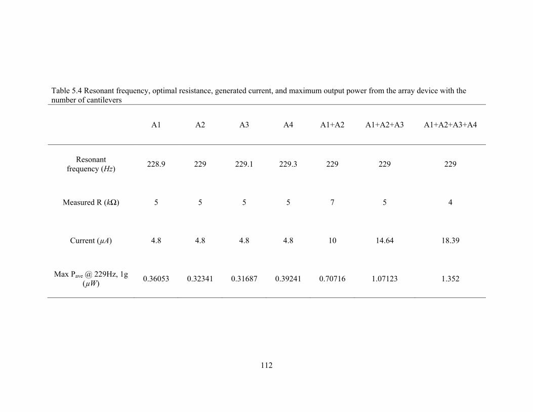
112
Table 5.4 Resonant frequency, optimal resistance, generated current, and maximum output power from the array device with the number of cantilevers
A1 A2 A3 A4 A1+A2 A1+A2+A3 A1+A2+A3+A4
Resonant frequency (Hz) 228.9 229 229.1 229.3 229 229 229
Measured R (kΩ) 5 5 5 5 7 5 4
Current (µA) 4.8 4.8 4.8 4.8 10 14.64 18.39
Max Pave @ 229Hz, 1g (µW) 0.36053 0.32341 0.31687 0.39241 0.70716 1.07123 1.352

113
While the output voltages under the optimal resistance load for maximum power were
similar at the different resistive loads, the currents linearly increased by the number of
cantilevers due to the decrease of the optimal resistive load from 15 kΩ to 4kΩ. The current was
calculated using Vrms by Ohm’s law and is plotted in Figure 5.15. The device with four
cantilevers generated 18.4 µA and 1.352 µW, which is about 3.8 times higher than that of the
single cantilever in Table 5.4. The linear relationship between the number of cantilevers and
output results have shown that the device has lost a very small amount of electricity where the
resonant frequencies of the cantilevers are distributed at 0.4 Hz.
1 2 3 4
4
8
12
16
20
Max
cur
rent
(μA)
# of cantilever
Max current Optimal resistance
4
8
12
16
Optim
al resistance (KΩ
)
Figure 5.15 The generated current at the optimal resistance load as number of cantilevers in
parallel connection

114
The output voltages were recorded with the same trigger at the optimized resistor load of
4 kΩ for each cantilever and their parallel connections. The output voltages were converted to
current by Ohm’s law and plotted in Figure 5.16. The phase difference between the signals from
each cantilever was less than 10o. All signals were negatively shifted as much as 5 µA, and it
seems that the shift was induced due to the asymmetric structure of the unimorph cantilever
structure. The unimorph structure only has the transducer layer on one side of cantilever frame.
The neutral axis of cantilever is located at the middle of the Si under layer.
-0.004 -0.002 0.000 0.002 0.004-0.12
-0.08
-0.04
0.00
0.04
0.08
0.12
Time (sec)
Volta
ge (V
)
Input signal Cantilever 1 Cantilever 2 Cantilever 3 Cantilever 4 Cantileve 1+2 Cantilever 1+2+3 All
Figure 5.16 AC output of four cantilevers and their parallel connections
The results show that multi cantilever sources resonate in phase and amplify the output
signal without excess electric loss and space expenses by individual circuitries. The array design
can overcome the narrow bandwidth, as well as the insufficient output power of the vibration-
based energy harvester.

115
5.3.2.2 Serial connection
Two cantilevers were wired in serial connection to increase the output voltage and power.
Each cantilever was isolated, and its bottom electrodes were opened by dry etching. An
evaluation of the device was performed under 0.25g acceleration and 129.8 Hz, and their output
voltage and power was plotted in Figure 5.16.
10 20 30 40 50 60
40
80
120
160
200
240
280
320
Rload (kΩ)
Vpk
-pk
C1 C2 C1+C2 serial
10 20 30 40 50 600.00
0.05
0.10
0.15
0.20
0.25
0.30
0.35
0.40
0.45
Rload (kΩ)
Out
put p
ower
(μW
) C1 C2 C1+C2 serial
Figure 5.17 Output peak voltage and power as resistance load from serial connected array
Both cantilevers have the same resonant frequency. The serial array generated 240 mV
and 0.35 µW, which are respectively 88% and 70% from the sum of the individual cantilevers,
while the currents were similar at the different optimal resistive loads.
The array device consists of two cantilevers with serial connections between the
cantilevers, and its output voltage was measured as shown in Figure 5.17. Each cantilever was
directly connected without an AC-DC rectifier, and the serial connection increases the output

116
voltage if the signal is in phase as shown in Figure 5.18.
Figure 5.18 The generated current at the optimal resistance load as number of cantilever in serial connection
The array cantilever can increase the voltage or current as a type of connection depending
on the requirements of the application and the specification of power management circuits.
5.4 Uniform stress contribution
Much attention has been focused on developing the design of piezoelectric films to
distribute the strain on the films and to increase the power density. The rectangular cantilever

117
beam is commonly chosen due to its high mechanical strain during environmental vibration and
simple design for microfabrication, but most of stress is driven to near the anchor of the
cantilever beam. This non-uniform distribution weakens the strength of the structure and reduces
the conversion efficiency, since the piezoelectric charge is not always proportional to the strain
induced by the stress. Baker et al. has introduced a trapezoidal-shaped cantilever for higher
efficiency in bulk scale, which increased the power output as much as 30% as compared to
rectangular cantilevers [91]. Although considerable research has been devoted to simulating the
strain distribution according to the shape of the cantilever, rather less attention has been paid to
analyzing it experimentally in MEMS devices. This study is designed to analyze the strain
distribution according to the cantilever geometry and verify it experimentally using the local
output power from different positions. Both trapezoidal- and rectangular-shaped cantilevers were
applied on this experiment. This study gives preliminary and experimental results for improving
the power density by the strain distribution on the surface of the MEMS energy harvesting
device.
The geometry change in the cantilever shape may distribute the strain on the piezoelectric
film and improve the power output due to nonlinear piezoelectric properties, even in the MEMS
scale. The generated powers were separately collected from different positions, and they had
good agreement with the strain estimation from finite element analysis.
To improve the stress uniformity, two structure configurations were proposed as shown
in Figure 5.19. One has a different thickness, and the other has a different width in the
longitudinal direction of the cantilever. Since the formal one requires a different fabrication
method in the MEMS process, the second one was chosen for this experiment. In this section,

118
the distribution of stress according to the cantilever shape will be inspected using a trapezoid-
shaped cantilever.
Figure 5.19 The structure for uniform stress distribution
The size of both cantilevers was 4x2 (L x W) for the beam and 3x2x0.5 (L x W x H) for the
mass in unit of mm. The trapezoidal cantilever had the reduced width at the mass of 1 mm. The
platinum electrodes were separately patterned on each cantilever near the anchor, middle, and the
mass, as seen in Figure 5.20. Since the direct wire bonding might affect to the vibration motion
of the device or failure of wiring, the thin film wires were also patterned on the PZT surface
from the electrodes to the contact pads. The wiring on the contact pad was constructed with a
hand-made polymer packaging for the top electrode and silverpaste for the bottom contact.

119
Figure 5.20 The configuration of electrode for geometric stress concentration: (a) rectangular, (b) trapezoidal. [98]
ABAQUS finite element modeling software was used to estimate the strain on the PZT
film. The modeling was performed using the real size of the device with loading static force as
much as 9.8 ms-2 of acceleration. The material properties of PZT film were as follows: Young’s
modulus was 69 GPa which was measured by nano indentation, Poison’s ratio was 0.3, and the
density was 2330 kgm-3. The material properties of Si were as follows: Young’s modulus was
160 GPa in (110), Poison’s ratio was 0.27, and the density was 7500 kgm-3. The modeling
considered SiO2 and its properties were as follows: Young’s modulus was 70 Gpa, Poison’s
ratio was 0.165, and the density was 2200 kgm-3. The local strains from each electrode were

120
obtained by averaging the strains of the mesh elements. The meshes were distributed on both
cantilevers, as shown in Figure 5.21.
Figure 5.21 The configuration of electrode and mesh elements on (a) rectangular and (b) trapezoidal cantilever [98]
The output powers were obtained from different locations for both cantilevers to
investigate the effect of stain distribution as a cantilever shape. The normalized power for each
electrode was plotted at a given resistive load under 2.45 ms-2 of acceleration, as seen in Figure
5.22 (a) and (b). To exclude the generated powers from the wire electrodes, the total power was
normalized into the real size of electrode area of 1 mm2. There were two limitations on this
normalization. Since the generated charge on piezoelectric material is not proportional to the
amount of strain, its nonlinearity should be considered on this normalization. The nonlinear
piezoelectric coefficient, however, was neglected in this study. The other limitation is that the
output powers were not exactly come from the square electrode pad as modeling. The resistive
loads of 20±1 kΩ were shifted, because the small differences between electrodes were caused by

121
the different sizes of electrodes, including the area of the wire before normalizing. The maximum
powers of each electrode were nevertheless used to compare them with the average strains from
FEM analysis, as shown in Figure 5.22 (c) and (d). The electrodes near the anchor showed the
highest normalized power in both cantilevers, while the power near the mass has the smallest
values. Now, it is important how much power was generated at the middle electrodes as
compared with that of the others. The powers from three electrodes showed a nonlinear
relationship, while the powers at the middle electrodes for rectangular and trapezoidal cantilevers
had smaller and larger values, respectively. If assuming that the materials in the cantilever
structure are linear, elastic, and isotropic with average stress applied along the 1-1 direction, the
output power is expressed as follows [12]:
2
31
2 1⎭⎬⎫
⎩⎨⎧
⎟⎠⎞
⎜⎝⎛=== L
LxEg
RRvP
LL
ε (5.5)
where x is the location from the clamped end, L is the length of beam, g is the piezoelectric
voltage constant, E is the Young’s modulus, and ε is the strain. In Figure 5.22(c), the relationship
between strain and power has been agreed with Equation (5.5). On the contrary, the trapezoidal
cantilever has a negative parabolic relationship. The reason is suggested that the strain
distribution has spread out into the region of the middle electrode in the trapezoidal cantilever
structure. The nonlinear piezoelectric coefficient (g31) might increase the total output power
through the entire PZT thin film. Unfortunately, the quantitative analysis of this result cannot be
accompanied at this time.
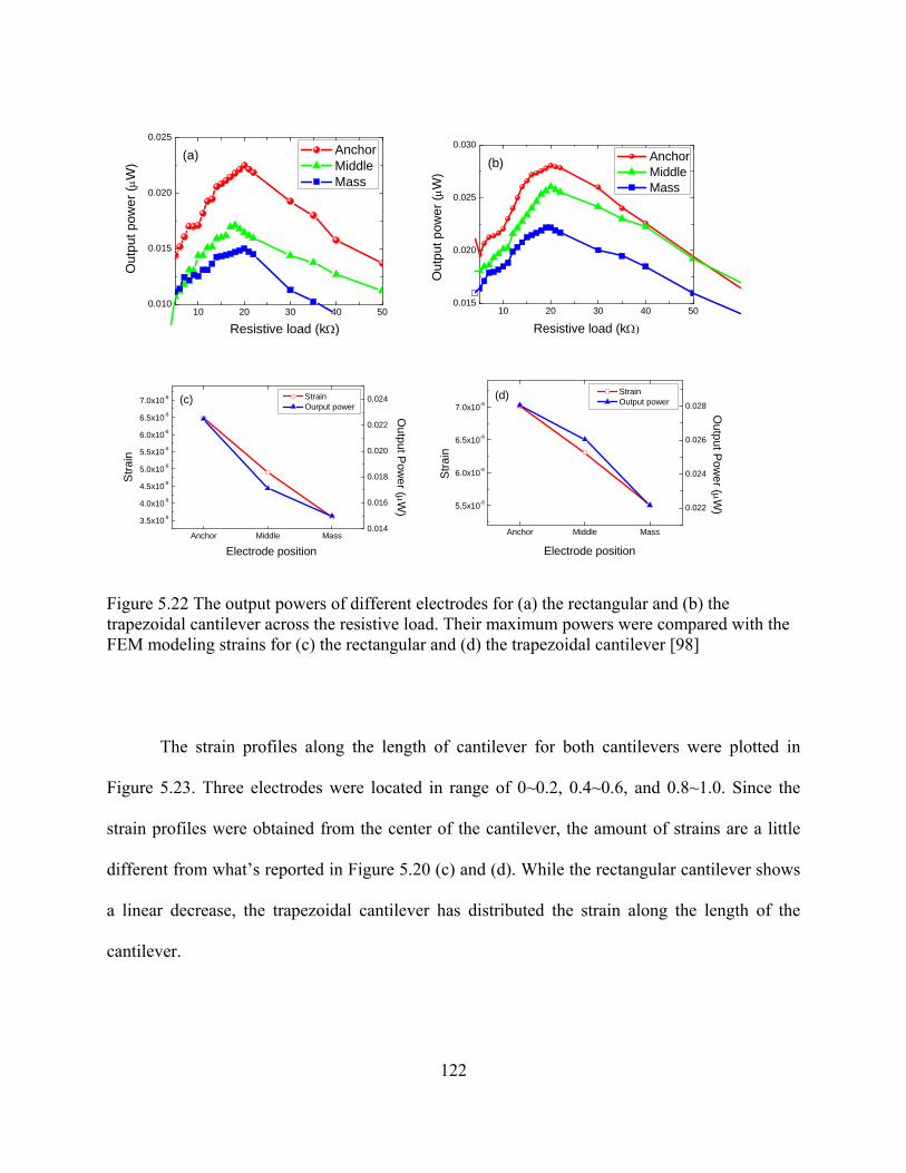
122
10 20 30 40 500.010
0.015
0.020
0.025
Out
put p
ower
(μW
) Anchor Middle Mass
Resistive load (kΩ)
(a)
10 20 30 40 500.015
0.020
0.025
0.030
Out
put p
ower
(μW
)
Resistive load (kΩ)
Anchor Middle Mass
(b)
Anchor Middle Mass
3.5x10⁻⁸
4.0x10⁻⁸
4.5x10⁻⁸
5.0x10⁻⁸
5.5x10⁻⁸
6.0x10⁻⁸
6.5x10⁻⁸
7.0x10⁻⁸
Electrode position
Stra
in
Strain Ourput power
(c)
0.014
0.016
0.018
0.020
0.022
0.024
Output P
ower (μW
)
Anchor Middle Mass
5.5x10⁻⁸
6.0x10⁻⁸
6.5x10⁻⁸
7.0x10⁻⁸
Output P
ower (μW
)
Stra
in
Electrode position
Strain Output power
(d)
0.022
0.024
0.026
0.028
Figure 5.22 The output powers of different electrodes for (a) the rectangular and (b) the trapezoidal cantilever across the resistive load. Their maximum powers were compared with the FEM modeling strains for (c) the rectangular and (d) the trapezoidal cantilever [98]
The strain profiles along the length of cantilever for both cantilevers were plotted in
Figure 5.23. Three electrodes were located in range of 0~0.2, 0.4~0.6, and 0.8~1.0. Since the
strain profiles were obtained from the center of the cantilever, the amount of strains are a little
different from what’s reported in Figure 5.20 (c) and (d). While the rectangular cantilever shows
a linear decrease, the trapezoidal cantilever has distributed the strain along the length of the
cantilever.

123
0.0 0.2 0.4 0.6 0.8 1.00
2x10⁻⁸
4x10⁻⁸
6x10⁻⁸
8x10⁻⁸
Stra
in
Normalized length
Rectangular Trapezoid
Figure 5.23 The strain profiles from anchor to mass for the rectangular and the trapezoidal-shaped cantilever [98]
When all electrodes were connected together, the output powers were measured for both
cantilevers to compare the total power. as seen in Figure 5.24. The maximum powers were
obtained at the same resistive load of 7 kΩ for both cantilevers. since the electrode area was
increased, the optimal resistive load was decreased compared to the small individual electrodes.
The output power from the trapezoidal cantilever was increased to 39% comparing with that of
the rectangular cantilever.
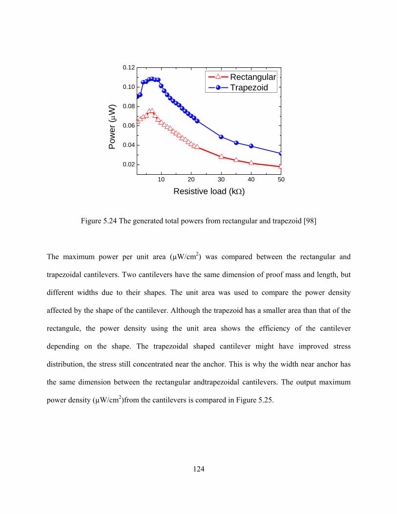
124
10 20 30 40 50
0.02
0.04
0.06
0.08
0.10
0.12
Pow
er (μ
W)
Resistive load (kΩ)
Rectangular Trapezoid
Figure 5.24 The generated total powers from rectangular and trapezoid [98]
The maximum power per unit area (µW/cm2) was compared between the rectangular and
trapezoidal cantilevers. Two cantilevers have the same dimension of proof mass and length, but
different widths due to their shapes. The unit area was used to compare the power density
affected by the shape of the cantilever. Although the trapezoid has a smaller area than that of the
rectangule, the power density using the unit area shows the efficiency of the cantilever
depending on the shape. The trapezoidal shaped cantilever might have improved stress
distribution, the stress still concentrated near the anchor. This is why the width near anchor has
the same dimension between the rectangular andtrapezoidal cantilevers. The output maximum
power density (µW/cm2)from the cantilevers is compared in Figure 5.25.

125
Rectangular Triangle
Pow
er d
ensi
ty (μ
W/c
m2 )
Cantilever shape
Figure 5.25 The output maximum power as cantilever shape
5.5 Comparison between 31 mode and 33 mode
The 31 mode and 33 mode piezoelectric energy harvesters were fabricated using the same
dimensions and same quality PZT film on Pt film. When the strain is loaded in a longitudinal
direction of the cantilever, the top and bottom electrodes are normal to the strain, and
interdigitated electrode (IDE) collected the discharge directly to the strain. The schematic
illustrations of the two modes are shown in Figure 5.26. A simple comparison of output power
for the two different modes does not have much meaning because they have their own
piezoelectric characteristics for energy harvesting applications. Furthermore, output power from
the 33 mode strongly depends on the configuration of IDE.

126
(a) (b)
Figure 5.26 Schematic illustration of 31 mode (a) and 33 mode (b) cantilevered piezoelectric
energy harvester
The 31 mode conversion usually generates a high current with a low impedance due to the
large electrode area. On the contrary, a relativly small output voltage might be the limitation of
this mode. The output voltage is decided by the thickness of the piezoelectric film between the
top and bottom electrodes, since the output voltage (Voc) under open circuit is defined by
Equation 5.6.
HgV xxoc 31σ= (5.6)
where σxx is stress on the length of cantilever, g31 is the piezoelectric constant of 31 mode, and H
is the thickness between the top and bottom electrodes.
The output of the 33 mode conversion using IDE is more complex because the electrode area
and the distance between the two electrodes varies by dimensions of width and gap in IDE.
Figure 5.27 is a simple illustration of IDE and shows dimensional notations.

127
Figure 5.27 Schematic of IDE
The output voltage from IDE is decided by the distance (l) between the finger electrodes, and
the output voltage (Voc) under open circuit is defined by Equation 5.7.
lgV xxoc 33σ= (5.7)
where g33 is the piezoelectric constant of the 33 mode. The expected voltage level can be
obtained in the 33 mode conversion by adjusting the distance (l). In the mean time, the 33 mode
conversion generates a low current with high impedance. As the distance (l) increases to obtain
the high voltage level, the number of fingers is reduced in the limited length (L) of the cantilever.
When the electrode area (A) of IDE is defined by Equation 5.8, the impedance is the same as the
optimal resistive load (Ropt) where the maximum power is obtained increase as shown in
Equation 5.10.
)1( −= NWtA (5.8)
lAC r 0εε= (5.9)

128
CfRopt ⋅⋅
=π2
1 (5.10)
where t is the thickness of piezoelectric film, N is the number of IDE finger, C is the capacitance,
ε0 is the permittivity of vacuum, εr is dielectric constant, and f is the resonant frequency.
When poling PZT using IDE, the entire film cannot be poled in a longitudinal direction due
to the area under the electrode area. The unpoled area under the electrodes is called dead zone as
shown in Figure 5.28.
Figure 5.28 Poling directions on IDE with show dead zone as a grey color
The dead zone can be reduced by deciding the width of the electrode considering the
thickness of PZT, such as 0.8 ratio of width to thickness [99]. While the large thickness of PZT
is limited in film technology, the width of electrode is hardly reduced in few microns due to
lithography process. Although the 33 mode piezoelectric constant may be larger than the 31
mode, the output powers from the two different modes are hardly compared due to the limitation
of IDE.
5.5.1 Poling effect on 31 mode and 33 mode
The dipoles of as-deposited PZT thin film has random orientation and the film show no

129
piezoelectric character due to zero net-polarization. When the film has poled in proper condition,
it shows the maximum piezoelectric properties which mostly increase the efficiency of PEH. The
bulk PZT, which has no internal field and no stress, has symmetry piezoelectric response. In the
contrary to the bulk PZT, PZT thin film has asymmetry character due to its residual stress,
defective region created during the deposition, or internal field. The poling condition should be
adjusted considering the asymmetry condition of the films. In this chapter, the poling conditions
were optimized and the output performance of PEH simultaneously investigated as the poling
conditions.
Poling effect on d31 mode
The P-E hysteresis loop was given in Figure 5.29 for the PZT film on PEH which had
dimension in 4100 x 500 µm. The loop had saturated polarization in 200 kV/cm and gave about
20 µC/cm2 of the remnant polarization and about 32 kV/cm of coercive field. The loop was
shifted -7 kV/cm along the field axis, and the shift was preserved after several tests. It was
assumed that the shift is caused from the internal field. The internal field seems to be created
during the etching by RIE, since the shifted field had same direction with the bias during plasma
etching. The internal field was probably induced by energetic bombardment or ion peening
during RIE. The other assumption is that the tensile residual stress shift the loop [100, 101].

130
-20 -10 0 10 20
-40
-20
0
20
40
Voltage (V)
Polarization (μC/cm2)
Figure 5.29 Polarization hysteresis loop for the PZT film on PEH
The effect of poling direction under existed internal field was investigated. Figure 5.30 gives
the output power versus the resistive load under 0.25 g acceleration force as poling conditions at
room temperature. The negative poling field which is in a direction antiparallel to the internal
field gained small output powers, while the film poled in the direction parallel with positive field
on the top show higher efficiency of PEH. It is believed that the change of the output power
caused from the internal field. It is reported that the piezoelectric constant decrease by the poling
in a direction antiparallel to the internal field [102, 103] varies by the poling direction, and the
results has good agreement with them.
A slight increase of the output power in positive poling field was shown as the poling time
from 1 second to 15 min. In the contrary, the negative poling field in short time had much
smaller output power since it is insufficient due to existed opposite internal field.
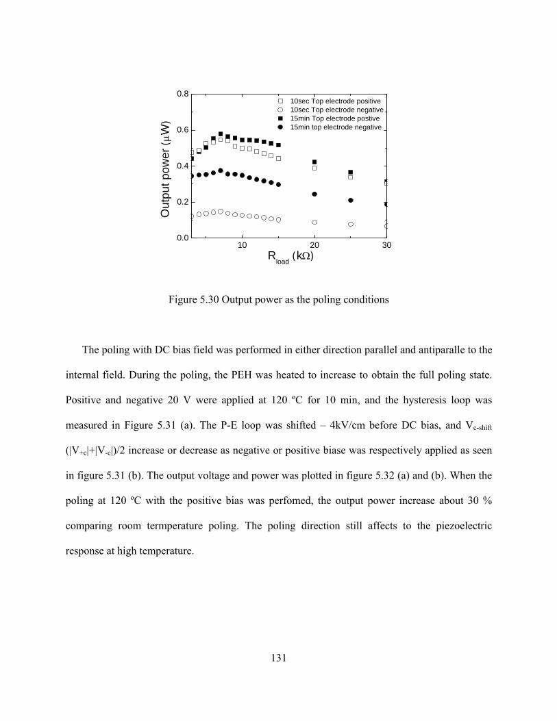
131
10 20 300.0
0.2
0.4
0.6
0.8
Rload (kΩ)
Out
put p
ower
(μW
)
10sec Top electrode positive 10sec Top electrode negative 15min Top electrode postive 15min top electrode negative
Figure 5.30 Output power as the poling conditions
The poling with DC bias field was performed in either direction parallel and antiparalle to the
internal field. During the poling, the PEH was heated to increase to obtain the full poling state.
Positive and negative 20 V were applied at 120 ºC for 10 min, and the hysteresis loop was
measured in Figure 5.31 (a). The P-E loop was shifted – 4kV/cm before DC bias, and Vc-shift
(|V+c|+|V-c|)/2 increase or decrease as negative or positive biase was respectively applied as seen
in figure 5.31 (b). The output voltage and power was plotted in figure 5.32 (a) and (b). When the
poling at 120 ºC with the positive bias was perfomed, the output power increase about 30 %
comparing room termperature poling. The poling direction still affects to the piezoelectric
response at high temperature.
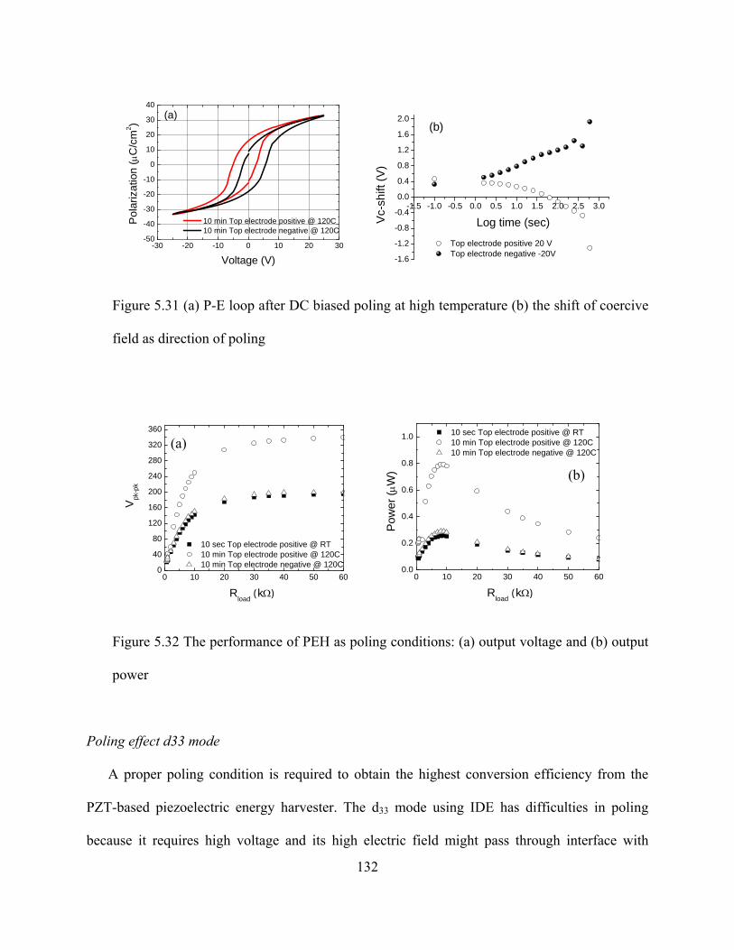
132
-30 -20 -10 0 10 20 30-50
-40
-30
-20
-10
0
10
20
30
40
Pol
ariz
atio
n (μ
C/c
m2 )
Voltage (V)
10 min Top electrode positive @ 120C 10 min Top electrode negative @ 120C
(a)
-1.5 -1.0 -0.5 0.0 0.5 1.0 1.5 2.0 2.5 3.0
-1.6
-1.2
-0.8
-0.4
0.0
0.4
0.8
1.2
1.6
2.0
Log time (sec)Vc-
shift
(V)
Top electrode positive 20 V Top electrode negative -20V
(b)
Figure 5.31 (a) P-E loop after DC biased poling at high temperature (b) the shift of coercive
field as direction of poling
0 10 20 30 40 50 600
40
80
120
160
200
240
280
320
360
V pk-p
k
Rload (kΩ)
10 sec Top electrode positive @ RT 10 min Top electrode positive @ 120C 10 min Top electrode negative @ 120C
0 10 20 30 40 50 600.0
0.2
0.4
0.6
0.8
1.0
Rload (kΩ)
Pow
er (μ
W)
10 sec Top electrode positive @ RT 10 min Top electrode positive @ 120C 10 min Top electrode negative @ 120C
Figure 5.32 The performance of PEH as poling conditions: (a) output voltage and (b) output
power
Poling effect d33 mode
A proper poling condition is required to obtain the highest conversion efficiency from the
PZT-based piezoelectric energy harvester. The d33 mode using IDE has difficulties in poling
because it requires high voltage and its high electric field might pass through interface with
(a)
(b)

133
substrate or surface of PZT film. The PZT film (4000 x 2000 µm) which has IDE (20 µm
electrode width and 40 µm gap) was sampled, and its hyteresis loop was obtained up to 200
kV/cm in a silicon oil bath as shown in Figure 5.33 (a). The electrode area was defined by
Equation 5.8. The slant loop was obtained with saturated remant polarization at 100 kV/cm and
linear increase of maximum polarization as electric field. A possible reason of the slanted loop is
the existed non-ferroelectric regions between electrodes or space charge which retrict the domain
motions. When inspecting the crystallization of the PZT film on ZrO2 in Figure 5.33 (b), the PZT
film was well-oriented without pyrochloride phase. The different microstructure along the
longditudinal axis probably induced the space charge, but its deeper study should be followed. it
is well oriented to and The wide gap between electrode in IDE
-800 -400 0 400 800
-200
-150
-100
-50
0
50
100
150
200
Pol
ariz
atio
n (μ
C/c
m2 )
Voltage (V)
200V 400V 600V 800V
(d)20 30 40 50 60
PZT
(002
)
PZT
(111
)
PZT
(011
)
INte
nsity
(arb
. uni
t)
2θ
PZT
(100
)/(00
1) PTO peaks are not labeled
Figure 5.33 The characterization of the PZT film in d33 mode PEH: (a) hysteresis loop & (b)
XRD analysis
The output voltages as the poling conditions were plotted in Figure 5.34 (a). A longer poling
time for 20 min was inspected to obtain a full poling state. When poling electric field was
increase from 25 to 100 kV/cm at room temperature, the output voltage at a open circuit
saturated from 62.5 kV/cm. The PZT film seems to be damaged under 100 kV/cm DC bias
(a) (b)

134
poling for 20 min. In figure 5.34 (a), the output voltages are same under two poling conditions
between the short time 200 kV/cm AC poling at room temperature and the long time 62.5 kV/cm
DC poling at 100 ºC. Further increase of DC bias poling could not be performed due to a
breakdown.
0 2000 4000 6000 8000 100000
50010001500200025003000350040004500500055006000
Vpk
-pk (m
V)
Resistive load (kΩ)
RT 100V RT150V RT 200V DC RT 250V DC RT 300V DC RT 800V AC 100C 250V DC
100 150 200 250 300 350 400
1000
2000
3000
4000
5000
6000
7000
Out
put v
olta
ge(m
V)
Poling voltage (V)
Figure 5.34 (a)output voltage as different poling conditions & (b) output voltage at open-circuit
as poling field
5.5.2 Outputs in 31 mode and 33 mode
The output voltage and power were measured and plotted for two different modes in Figure
5.29 (a) & (b) under same poling condition of 200 kV/cm electric field. Under 0.25 g of
acceleration condition, the 31 mode had 127.2 Hz of resonant frequency and the 33 mode has a
little lower frequency at 118.1 Hz. The difference induced by the configuration of top electrode.
The IDE has a 20 µm width and 40 µm distance between the finger electrodes, so a total of 67
fingers make up the length of the cantilever. Output voltage from d33 mode is 15 times larger
than that from d31 mode, not 40 times as distance increase between the electrodes. It seems that
high concentration of grain boundaries across the finger electrodes in IDT makes more pinning

135
of the domain walls and reduce the piezoelectric response. Max power from 3-1 mode is 2
times higher than that from 3-3 mode due to its 28 times larger current with small optimal
resistive load. Both modes were sufficiently poled in 200 kV/cm of electric field where the film
exhibits reasonable ferroelectric properties. The remnant polarizations of 31 and 33 modes
respectively were 20 and 32 µC/cm2, and the coercive electric field was ~31 kV/cm for both
films.
0 5 10 15 20 25 30 35 400
50
100
150
200
250
300
350
400
450
Resistive load (kΩ)
Vpk
-pk (m
V)
0.0
0.2
0.4
0.6
0.8
1.0
Pow
er (μW)
(a)0 2000 4000 6000 8000 10000
0
1000
2000
3000
4000
5000
6000
Resistive load (kΩ)
V pk-p
k (m
V)
0.0
0.1
0.2
0.3
0.4
0.5
Pow
er (μW)
(b)
Figure 5.35 The comparison between 31 and 33 mode conversion based on cantilever
displacement: (a) output from 31 mode, (b) output from 33 mode
Table 5.5 Comparison between d31 and d33 mode d31 mode d33 mode
Distance 1 µm 40 µm
Dimensions 7x2mm (4x2 mm cantilever, 3x2 mm mass)
R.F. (Hz) 127.2 118.1 Hz
Poling conditions 200 KV/cm AC @ RT
Optimal R (kΩ) 10 4000
Output Voltage (mV) 271 3885
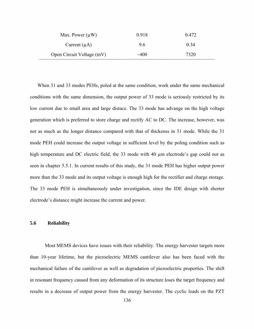
136
Max. Power (µW) 0.918 0.472
Current (µA) 9.6 0.34
Open Circuit Voltage (mV) ~400 7320
When 31 and 33 modes PEHs, poled at the same condition, work under the same mechanical
conditions with the same dimension, the output power of 33 mode is seriously restricted by its
low current due to small area and large distace. The 33 mode has advange on the high voltage
generation which is preferred to store charge and rectify AC to DC. The increase, however, was
not as much as the longer distance compared with that of thickenss in 31 mode. While the 31
mode PEH could increase the output voltage in sufficient level by the poling condition such as
high temperature and DC electric field, the 33 mode with 40 µm electrode’s gap could not as
seen in chapter 5.5.1. In current results of this study, the 31 mode PEH has higher output power
more than the 33 mode and its output voltage is enough high for the rectifier and charge storage.
The 33 mode PEH is simultaneously under investigation, since the IDE design with shorter
electrode’s distance might increase the current and power.
5.6 Reliability
Most MEMS devices have issues with their reliability. The energy harvester targets more
than 10-year lifetime, but the piezoelectric MEMS cantilever also has been faced with the
mechanical failure of the cantilever as well as degradation of piezoelectric properties. The shift
in resonant frequency caused from any deformation of its structure loses the target frequency and
results in a decrease of output power from the energy harvester. The cyclic loads on the PZT

137
cantilever may induce the deterioration of structure on both structure and PZT. The created
cracks on PZT film reduce the piezoelectric response, and the cracks on the Si substrate may
result in the instantaneous failure of the structure due to its brittle structure of single crystalline.
The possible mechanical failure and degradation of device are listed on Table 5.5.
Table 5.5 Reliability issued on Si-based PZT cantilever
Structure failure Piezoelectric PZT
Facture or fatigue
- Overload fracture
- Fatigue fracture
Delamination
Depoling due to
- Mechanical load
- Temperature
Leakage current
- microcracks
The failure of structure might be caused from fracture or fatigue under overload of high
acceleration or cyclic load, respectively. The delamination between the PZT active layer
(Pt/PZT/Pt) and the substrate or generated cracks might induce a shift of resonant frequency or
failure of Ohmic contact between the PZT and electrode, which results in decreasing output
power due to the resonant frequency. The cyclic load or high temperature might induce the
depoling of PZT, or generated microcracks could result the in unrecoverable degradation of PZT.
In this section, the reliability of energy harvester will be investigated in structure damage and
degradation of PZT film by mechanical and environmental impacts.
5.6.1 Structural failure by fatigue
The PZT cantilever was designed considering the mechanical strength of PZT compared

138
to the maximum stress on PZT, and the safety factor (σyield/σmax at 1g acceleration) was already
estimated in Chapter 4. The safety factor was calculated using the average stress on the surface
of structure, and the device should stand up to several gravity forces (G). The structural failure,
however, occurred before the estimated point during experiments. Although errors in estimation
exist, early failure of the structure can be caused by other reasons. The microstructural
investigation of failure in the cantilevered structure was performed. Since the notch test for
fatigue for the MEMS cantilever is technically restricted, the fractured surface was investigated
by SEM in Figure 5.30.

139
(a) (b) (c)
(d) (e) (f)
Figure 5.36 SEM image of fractured surface of cantilever
:
SiO2
Si
PZT

140
The cantilevered structure failed due to the cyclic load of high acceleration. It was
resonated for 5 minutes each under 0.75, 1, 1.25, 1.5, 1.75, and 2 g acceleration conditions. The
failure occurred near the anchor, and the wide range of the fractured surface was inspected. The
single crystal of Si has almost four times higher fracture toughness than that of PZT thin film.
While the Si has below 1.94 MPa√m of toughness, the PZT thin film has below 0.5 MPa√m [92-
94]. The fatigue propagation should be nucleated and grown from a PZT surface that has low
toughness if they are under same amount of cyclic load, but the crack was initiated from the Si
surface and generated failure quickly. When inspecting the fractured surface, it was found that
the origin of fracturewas located some place in the middle as seen in Figure 5.30(c). It seems that
the crack started from the base side across the SiO2 layer. From this point, the water marks were
found on the entire cantilever and they emanate toward the outside in a regular pattern. Figure
5.30 (a) & (b) show the left side from the origin of crack and Figure 5.30 (d)~(f) show the right
side. The etching surface by RIE is not perfectly smooth (based side in Figure 5.30), and it seems
that the rough surface created the initial crack. They have played role of initial crack, and the Si
failed prior to the PZT film in spite of its higher toughness. The substitute of substrate material is
restricted in the MEMS process, but the polymer might be one of the possible materials using the
techniques of polymer MEMS. These questions remain to be answered in future work based on
this study.
5.7 Degradation of PZT
5.7.1 Degradation during fabrication
The degradation in piezoelectric properties of PZT thin film during the microfabrication
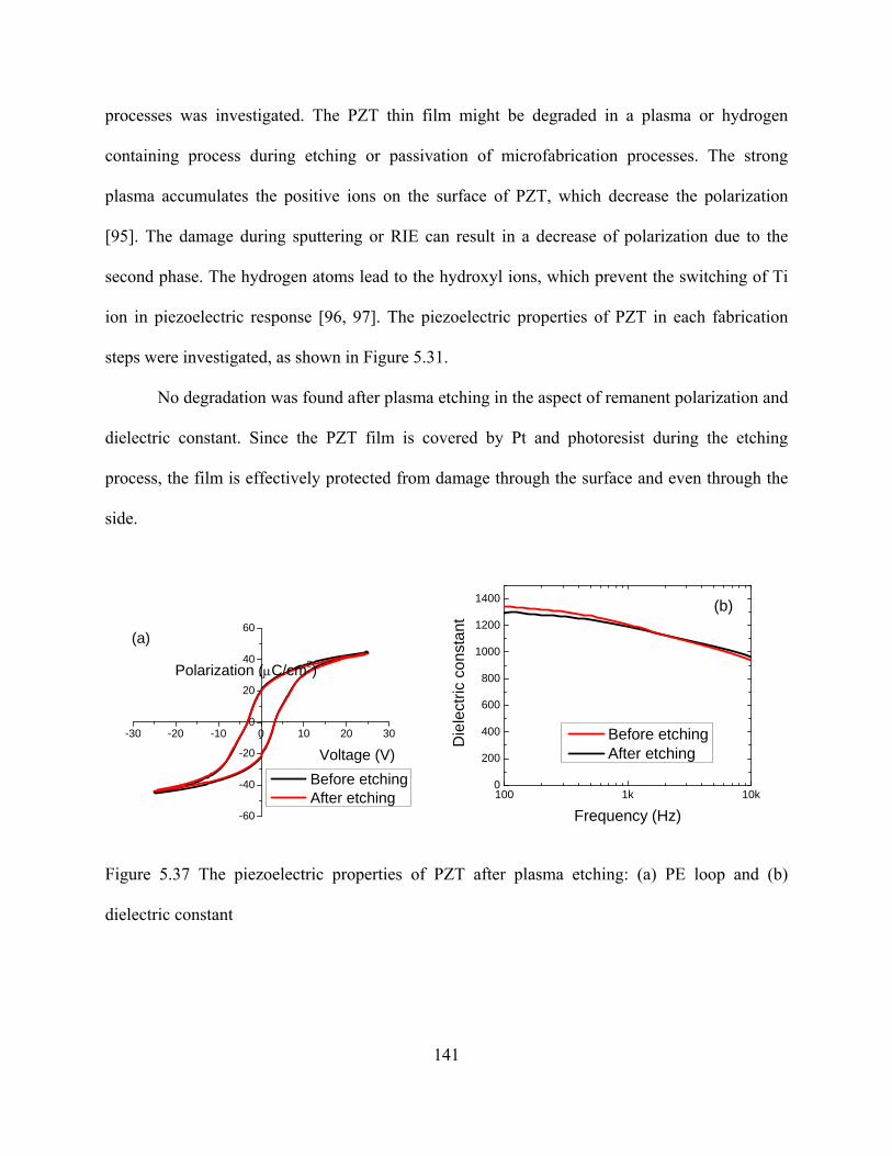
141
processes was investigated. The PZT thin film might be degraded in a plasma or hydrogen
containing process during etching or passivation of microfabrication processes. The strong
plasma accumulates the positive ions on the surface of PZT, which decrease the polarization
[95]. The damage during sputtering or RIE can result in a decrease of polarization due to the
second phase. The hydrogen atoms lead to the hydroxyl ions, which prevent the switching of Ti
ion in piezoelectric response [96, 97]. The piezoelectric properties of PZT in each fabrication
steps were investigated, as shown in Figure 5.31.
No degradation was found after plasma etching in the aspect of remanent polarization and
dielectric constant. Since the PZT film is covered by Pt and photoresist during the etching
process, the film is effectively protected from damage through the surface and even through the
side.
-30 -20 -10 0 10 20 30
-60
-40
-20
0
20
40
60
Polarization (μC/cm2)
Voltage (V) Before etching After etching
(a)
100 1k 10k0
200
400
600
800
1000
1200
1400
Die
lect
ric c
onst
ant
Frequency (Hz)
Before etching After etching
(b)
Figure 5.37 The piezoelectric properties of PZT after plasma etching: (a) PE loop and (b)
dielectric constant

142
5.7.2 Reliability during cyclic load
PZT film has degradation of its piezoelectric properties as electric or mechanical cyclic
load. Adding to the mechanical failure, the cyclic load might induce the mechanical or electrical
degradation to the PZT film such as cracks or depoling. Since the energy harvester only
encounters the mechanical load, its performance was inspected for up to three days in a
continuous cyclic load. Under 0.5 G acceleration and open circuit conditions, the output voltage
from the device was monitored with the resonant frequency, as shown in Figure 5.32. When the
temperature on the PZT film was monitored, no heating up was found during the entire cyclic
load.
106 107 108
252
256
260
264
268
272
276
280
284
288
# of Cycles
1Mohm ResonantfrequencyOut
put v
olta
ge (m
V)
Repoling230.0
230.2
230.4
230.6
230.8
231.0
Resonant frequency (H
z)
Figure 5.38 Output voltage and resonant frequency as number of cyclic load

143
After 5x10⁶ cycles, the output voltage started to decrease from 280 mV without any shift
of resonant frequency. Since the resonant frequency is constant, the change of output voltage is
not caused from out of maximum output at the natural frequency of the device but because of the
degradation of piezoelectric conversion. The decrease was slightly saturated at 260 mV around
2x10⁷ cycles. At 2.3x10⁷ cycles, the PZT was poled again with the same conditions. After the
second poling, the output voltage recovered slightly higher than that of first poling. The reason
that the output voltage fluctuated is not explained, but the output voltage was saturated at 282
mV. The resonant frequency was still constant. The results show that the PZT had depolarization
during the resonating, not generating microstructural defects.
5.7.3 Reliability under high temperature
The performance of the energy harvester was investigated at the high temperature, since
it can be exposed to a harsh environment of temperature. The high temperature affects the
structural stiffness and material properties of PZT. The Young’s modulus, density of materials,
and damping ratio have different values at high temperatures, and it is expected that the natural
frequency of the device or change in the magnitude of displacement under same acceleration
condition. The expansion of the dimensions might be neglected in the influence to the shift of the
natural frequency. The dielectric and piezoelectric constants tend to increase and reach their
maximum at Curie temperature, since a low energy barrier makes it easy to polarize the materials
at a high temperature. The conversion efficiency of PZT film itself should be affected by
temperature.
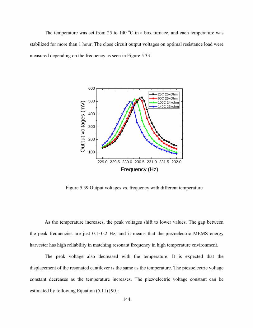
144
The temperature was set from 25 to 140 oC in a box furnace, and each temperature was
stabilized for more than 1 hour. The close circuit output voltages on optimal resistance load were
measured depending on the frequency as seen in Figure 5.33.
229.0 229.5 230.0 230.5 231.0 231.5 232.0
100
200
300
400
500
600O
utpu
t vol
tage
s (m
V)
Frequency (Hz)
25C 25kOhm 60C 25kOhm 100C 24kohm 140C 23kohm
Figure 5.39 Output voltages vs. frequency with different temperature
As the temperature increases, the peak voltages shift to lower values. The gap between
the peak frequencies are just 0.1~0.2 Hz, and it means that the piezoelectric MEMS energy
harvester has high reliability in matching resonant frequency in high temperature environment.
The peak voltage also decreased with the temperature. It is expected that the
displacement of the resonated cantilever is the same as the temperature. The piezoelectric voltage
constant decreases as the temperature increases. The piezoelectric voltage constant can be
estimated by following Equation (5.11) [90]:

145
T
dgεε 0
3131 = (5.11)
where g31 is the transverse piezoelectric voltage constant, d31 is the piezoelectric strain constant,
ε0 is the permittivity of vacuum, and εT is the relative dielectric constant at certain temperature.
20 40 60 80 100 120 140
230.2
230.3
230.4
230.5
230.6
230.7
Res
onan
t fre
quen
cy (H
z)
Temperature (oC)
Up Down
Figure 5.40 Resonant frequency’s shift as temperature
The change of resonant frequency was inspected according to temperature in Figure 5.34.
When the temperature increased up to 140 oC and then decreased to room temperature, the
frequency where the peak voltage existed was measured in both ways. The cantilever has been
resonated from start to end of experiments. The shift in resonant frequency caused from the long-
term cyclic load was neglected based on the results in the previous section. This experiment was
performed to investigate any structural damage of films and their interfaces like dilamination

146
during exposure to high temperatures. The shift of resonant frequency had good agreement with
the results in Figure 5.35, and the resonant frequency was perfectly recovered to that at room
temperature after being exposed to high temperature.
20 40 60 80 100 120 140740
760
780
800
820
840
860
880
O
utpu
t vol
tage
s (m
V) @
1MΩ
Temperature (C)
Figure 5.41 The output voltage vs. temperature with open circuit
The output voltage as temperature was inspected, as shown in Figure 5.35. This
experiment is performed to investigate the degradation of the piezoelectric properties. The output
voltage was measure with 1 MΩ of resistive load during times when the temperature goes up and
down. When the temperature increased, the output voltage decreased similar to what was seen in
previous results. The linearity between the temperature and output voltage is excluded in this
study. On the contrary, the output voltage could not be recovered to the initial value at room
temperature during cooling down. It seems that the piezoelectric properties of PZT had
degradation during exposure to high temperatures. The maximum temperature of this experiment

147
is not too high to make a large depolarization. Based on the small decrease of output voltage, a
bit of depolariziation occurred at that temperature. Followed a poling process, the initial output
voltage was recovered.

148
CHAPTER 6 CONCLUSIONS AND FUTURE WORK
6.1 Summary and conclusions
The present study works for demonstrating and developing the piezoelectric MEMS
energy harvester to increase the efficiency of energy conversion. The mechanical vibration
energy is converted into electrical energy by successful integration of piezoelectric thin films
into microsystems based on silicon. Advance MEMS processes are also developed for robust
fabrication. Based on the demonstration of the device, the advanced design is developed to
enhance the performance.
Chemical solution deposition with optimal heat treatment was used to deposit PZT thin
film, which exhibits the highest piezoelectric coefficient at the composition of morphotropic
phase boundary. The substrate of the Pt/adhesive layer largely affected the piezoelectric
properties of the PZT thin film. Proper material selection of Ti and thickness control prevented
the deterioration of the piezoelectric properties. Further study on thickness of PZT proved that 1
µm is the optimum thickness between the piezoelectric property and squandering deposition
process.
The demonstrated single cantilever has dimensions of 4 x 2 x 0.021 mm for the beam and
3 x 2 x 0.5 mm for the silicon proof mass, and the total volume was 3.294mm3. Under 0.5 g
acceleration and 127 Hz conditions, the device generated 4.52 µW, 538 mVpk-pk, and the

149
maximum power was 1372 µW/cm3. To improve the conversion efficiency of piezoelectric
effect, the stress on PZT thin film was widely distributed by using a trapezoidal-shaped
cantilever. The trapezoidal shape has increased the power 39% higher than the rectangular shape
due to the nonlinear property of piezoelectricity. The local signals near anchor, middle, and mass
were first extracted from the MEMS energy harvester, and then they were analyzed comparing
simulated data in FEM modeling.
The design of the cantilever array was demonstrated with parallel and serial connection
between the cantilevers that have the same dimensions to multiply the current or voltage as the
number of cantilevers. The resonant frequency of the energy harvester wasvery close to the
estimation in the range of the ambient vibration range (100 ~ 300 Hz) with less than 2%
deviation. Advanced etching techniques and the buried etching stop enabled this fine tuning of
resonant frequency, and the cantilever array could multiply the raw signals without any
circuitries or loss of electricity. The results show the feasibility that a higher voltage or current
can be obtained by integrating multiple cantilevers on one chip.
Reliability is a major issue for most MEMS devices. The structural damage and
degradation of piezoelectric properties of PZT under cyclic load and high temperature were
investigated. Depolarization seems to begin after 5x10⁶ cycles, although no microstructural
defect existed at that acceleration force. The decrease caused from depolarization was saturated
after 2x10⁷ cycles and was recovered by following the cycles with a poling process. At high
temperatures up to 140 oC, the resonant frequency of the device was shifted but fully recovered
by cooling down. The output voltage also decreased at high temperatures, but it did not recover
to the initial output voltage after cooling down. Depolarization seems to occurr, since the initial
output voltage was obtained after the poling process that followed. The damage of PZT thin film

150
after plasma etching was also inspected.
6.2 Future work
Piezoelectric MEMS energy harvester sstill have insufficient energy conversion for the
target application of a VLSI wireless sensor or biosensor. Although the conversion efficiency of
piezoelectric thin film might be improved, it is restricted in the current thin film technology of
metal oxide films. PZT and PZT-based composite materials will be developed to increase the
conversion efficiency due to their excellent piezoelectric properties. Furthermore, the advanced
design will be developed to enhance the power density of energy harvester. Since the power
enhancement though the stress distribution was verified in this study, the future design will be
focused on stress distribution under an acceleration force. The quantitative estimation of
generated power would be accompanied as the shape change.
The Si-based MEMS energy harvest has insufficient mechanical strength and limitation
of design considering various environmental conditions due to the stiffness of Si. On the
contrary, the Si-based process is not avoidable considering the cost and heat treatment at high
temperature. Although the compound of metal oxide and polymer is actively studied in this field
to increase the mechanical toughness, the piezoelectric properties are not sufficient yet.
Replacing the silicon membrane with polymer material is proposed for future work. Since the
stiffness of polymer materials are relatively easy to control, the multilayer structure of PZT and
polymer might enhance both the mechanical strength and displacement under a low acceleration
force.

151
A more efficient mode of a piezoelectric system might be used for the MEMS energy
harvester. A higher piezoelectric constant can be obtained in the 33 or 15 modes as compared to
the 31 mode. If the configuration of the MEMS structure and electrode design of IDT are
considered, it is uncertain that the 33 mode generates a higher power than the 31 mode in spite of
its two times higher piezoelectric constant. The 15 mode (with about a four times higher
piezoelectric constant than the 31 mode) has not been developed due to its complex design in
MEMS structural configuration. The current study for the piezoelectric energy harvest is
working on developing the 33 mode, and advanced design for the 15 mode is still a challenge for
this device.
152
BIBLIOGRAPHY
[1] H.R. Trankler and O. Kanoun, “Recent advances in sensor technology” Instrumentation and
Measurement Technology Conference. Proceedings of the 18th IEEE 2001, 309-316.
[2] Shashank Priya and Daniel J. Inman , Energy harvesting technologies. 2008, New York: Springer.
[3] Dan Steingart, Shad Roundy, Paul K. Wright, James, and W. Evans , “Micropower materials development for wireless sensor networks” MRS Bulletin 2008, 33 408-409.
[4] S. Roundy, P.K. Wright, and J. Rabaey , “A study of low level vibrations as a power source for wireless sensor nodes” computer Communications 2003,26 1131-1144.
[5] Shad Roundy, Brian P. Otis, Yuen-Hui Chee, Jan M. Rabaey, and Paul Wright , “ A 1.9ghz rf transmit beacon using environmentally scavenged energy” IEEE Int. Symposium on Low Power Elec. and Devices, Seoul, Korea 2003.
[6] Xiaofan Jiang, Joseph Polastre, and David Culler , “Perpetual environmentally powered sensor networks” Information Processing in Sensor Networks, 2005. IPSN 2005. Fourth International Symposium on 2005,463- 468.
[7] M. Kishi, H. Nemoto, T. Hamao, M. Yamamoto, S. Sudou, M. Mandai, and S.Yamamoto, “Micro thermoelectric modules and their application to wristwatches as an energy source” Eighteenth International Conference 1999,301-307.
[8] M. Strasser, R. Aigner, M Franosch, and G. Wachutka , “Miniaturized thermoelectric generators based on poly-si and poly-sige surface micromachining” Sensors and Actuators A 2002,97-98535-542.
[9] M. Stordeur and I. Stark, “Low power thermoelectric generator-self-sufficient energy supply for micro systems” Proc. 16th Int. Conf. on Thermoelectrics, Dresden, Germany 1997,575-577.
[10] M H Schneider, J W Evans, P K Wright, and D Ziegler , “Designing a thermoelectrically powered wireless sensor network for monitoring aluminum smelters” Proc. IMechE Vol. 220 Part E: J. Process Mechanical Engineering 2006,181-191.
153
[11] J. H. bottner, J. Nurnus, A. Gavrikov, G. Kuhner, M. Jagle, C. Kunzel, D. Eberhard, g. Plescher, A. Schubert, and K.-H. schlereth , “New thermoelectric components using microsystems technologies” Journal of Microelectromechanical Systems 2004,13 414-420.
[12] Colby L. Bellew, Seth Hollar and K.S.J. Pister, “An soi process for fabrication of solar cells, transistors and electrostatic actuators” IEEE The 12th International Conference on Solid State Sensors, Actuators and Microsystems, Boston, June 8-12, 2003 2003,1075-1079.
[13] J. F. Randall, On ambient energy sources for powering indoor electronic devices. 2003, EPFL. p. 51.
[14] S Roundy and P KWright, “A piezoelectric vibration based generator for wireless electronics” Smart Mater. Struct. 2004,13 1131–1142.
[15] P. D. Mitcheson, T. C. Green, E. M. Yeatman, and A. S. Holmes , “Architectures for vibration-driven micropower generators” Journal of Microelectromechanical Systems 2004,13 429-440.
[16] S P Beeby, R N Torah, M J Tudor, P Glynne-Jones,T O’Donnell, C R Saha and S Roy, “A micro electromagnetic generator for vibration energy harvesting” J. Micromech. Microeng. 2007,171257–1265.
[17] S. Meninger, J.O. Mur-Miranda, R. Amirtharajah, A. P. Chandrakasan, and J. H. Lang, “Vibration-to-electric energy conversion” IEEE trans. VLSI Syst. 2001,964-76.
[18] S. Shearwood and R. B. Yates, “Development of an electromagnetic micro-generator” Electron. Lett. 1997,331883-1884.
[19] Bernard Jaffe, William R. Cook, and Hans Jaffe, Piezoelectric ceramics. Vol. 3. (1971), London and New York: Academic press.
[20] N. setter, Piezoelectric materials in devices. (2002), Lausanne EPFL Swiss Federal Institute of Technology.
[21] Tommi Riekkinen, “Fabrication and characterization of ferro- and piezoelectric multilayer devices for high frequency applications,” in Information and Natural Sciences. 2009, VVT: Vuorimiehentie.
[22] Luiz Francisco Malmonge; José Antonio Malmonge; Walter Katsumi Sakamoto, “Study of pyroelectric activity of pzt/pvdf-hfp composite” Materials Research 2003,6
[23] K. A. KLICKER, J. V. BIGGERS, R. E. NEWNHAM, “Composites of pzt and epoxy for hydrostatic transducer applications” Journal of the American Ceramic Society 2006,645-9.
[24] Dongna Shen, Song-Yul Choe, and Dong-Joo Kim, “Analysis of piezoelectric materials for energy harvesting devices under high-g vibrations” J. J. A. P. 2007,46(10A),6755-6760.

154
[25] Hyeoungwoo Kim, Impedance adaptation methods of the piezoelectric energy harvesting, in Materials engineering. 2006, Pennsylvania State University.
[26] Paul Muralt, “PZT thin films for microsensors and actuators: Where do we stand?” IEEE trans. on ultra. ferro. freq. cont. 2000,47(4),903-915.
[27] Shadrach Joseph Roundy, Energy scavenging for wireless sensor nodes with a focus on vibration to electricity conversion, in Mechanical Engineering. 2003, University of California, Berkeley.
[28] Kazumasa Hasegawa and Tatsuya shimoda, “Piezoelectric transducer and electrophoretic ink display apparatus using piezoelectric transducer,” U.S. Patent, Editor. 2005, Seiko Epson corporation: USA.
[29] Xifan Wu, David Vanderbilt, and D. R. Hamann, “Systematic treatment of displacements, strains, and electric fields in density-functional perturbation theory” Phy. rev. B 2005,72 035105.
[30] R. Jona and G. Shirane, Ferroelectric crystals. (1993), New York: Dover.
[31] D. Damjanovic, “Ferroelectric, dielectric and piezoelectric properties of ferroelectric thin films and ceramics” Reports on Progress in Physics 1998,61 1267.
[32] L.L. Hench and J. K. West, Principles of electronic ceramics. (1990), West Sussex, England: John Wiley & Sons.
[33] A.L.Kholkin, D.V.Taylor, and N. Sene, “Poling effect on the piezoelectric properties of lead zirconate titanate thin films” IEEE 1998,
[34] B. Jaffe, W. R. Cook Jr., and H. jaffe, Piezoelectric ceramics. (1971): Academic Press, Inc.
[35] C.R. Bowen, “Optimisation of interdigitated electrode for piezoelectric actuators and active fibre composites” J. Electroceram 2006,16 263-269.
[36] Ryan robert Knight, The analysis and testing of mems and macro scale piezoelectric devices, in Mech. Eng. 2007, University of Pittsburgh. p. 96-111.
[37] Marcin Marzencki, Yasser Ammar, Skandar Basrour, “Integrated power harvesting system including a mems generator and a power management circuit” Sensors and Actuators A 2008,145-146 363-370.
[38] Daniel Guyomar, Adrien Badel, Elie Lefeuvre, and Claude Richard, “Toward energy harvesting using active materials and conversion improvement by nonlinear processing” IEEE Transaction on Ultrasonics, Ferroelectrics, and Frequency Control 2005,52 584-595.
[39] Ottman, G. K., Hofmann, H. F., Bhatt, A. C. And Lesieseutre, G. A, “Adaptive piezoelectric energy harvesting circuit for wireless remote power supply” IEEE Transactions on Power Electronics 2002,17 669-676.

155
[40] Shu, Y. C. and Lien, I. C., “Analysis of power output for piezoelectric energy harvesting systems” Smart Materials and Structures 2006,151499-1512.
[41] Daniel Guyomar, Adrien Badel, Elie Lefeuvre, and Claude Richard, “Toward energy harvesting using active materials and conversion improvement by nonlinear processing” IEEE transactions on ultrasonics, ferroelectrics, and frequency control 2005,52(4),584-595.
[42 I. Demir, A.L. Olson, J.L. Skinner, C.D. Richards, R.F. Richards, D.F. Bahr, “High strain behavior of composite thin film piezoelectric membranes” Microelectronic Engineering 2004,75 12–23.
[43] F. Lu, H. P. Lee, and S. P. Lim, “Modeling and analysis of micro piezoelectric power generators for micro-electromechanical-systems applications” Smart Mater. Struct. 2004,13 57–63.
[44 M. Marzencki, B. Charlot. S. Basrour, M. Colin, and L. valbin, “Design and fabrication of piezoelectric micro power generators for autonomous microsystems” DTIP symposium on design testing integration and packaging of MEMS/MOEMS 2005,229-302.
[45] M. Marzencki, Y. Ammar and S. Basrour, “Integrated power harvesting system including a mems generator and a power management circuit” Solid-State Sensors, Actuators and Microsystems Conference, 2007. TRANSDUCERS 2007. International 2007,887-890.
[46] Y.B. Jeon, R. Sood, J.-h. Jeong, S.-G. Kim, “Mems power generator with transverse mode thin film pzt” Sensors and Actuators A 2005,12 216-22.
[47] H. B Fang, J. Z. Liu, Z. Y. Xu, L. Dong, L. Wang, D. Chen, B. C. Cai, and Y. Liu, “Fabrication and performance of mems-based piezoelectric power generator for vibration energy harvesting” J. Microelectronics 2006,37 1280-1284.
[48] B S Lee, S C Lin, W J Wu, X Y Wang, P Z Chang and C K Lee, “Piezoelectric MEMS generators fabricated with an aerosol deposition pzt thin film” J. Micromech. Microeng. 2009,19 065014.
[49] R Elfrink, T M Kamel, M Goedbloed,S Matova, D Hohlfeld, Y van Andel and R van Schaijk, “Vibration energy harvesting with aluminum nitride-based piezoelectric devices” J. Micromech. Microeng. 2009,19 094005.
[50] Dongna Shen, “The design, fabrication and evaluation of a mems pzt cantilever with an integrated si proof mass for vibration energy harvesting” J. Micromech. Microeng 2008,18 055017.
[51] Dongna shen, Jung-Hyun park, Jyoti Ajitsaria, song-Yul Coe, Howard C Wikle, and Dong-Joo Kim, “Micromachined pzt cantilever based on soi structure for low frequency vibration energy harvesting” Sensors and Actuators A 2009,154103-108.

156
[52] Kim, H, Bedekar, V, Islam, R, Lee, WH, Leo, D, and Priya, S, “Laser micro-machined piezoelectric cantilevers for mechanical energy harvesting” IEEE Ultrason. Freq. Ferroelect. Cntrl 2008,55 1900-1905.
[53] Marco Ferrari, Vittorio Ferrari, Michele Guizzetti, Daniele Marioli, Andrea Taroni, “Piezoelectric multifrequency energy converter for power harvesting in autonomous microsystems” Sensors and Actuators A 2008,14 2329–335.
[54] Jing-Quan Liua, Hua-Bin Fanga, Zheng-Yi Xub, Xin-Hui Maob, Xiu-Cheng Shena, Di Chena, Hang Liaob, Bing-Chu Caia, “A mems-based piezoelectric power generator array for vibration energy harvesting” Microelectronics Journal 2008,39 802–806.
[55] E. Hong, J.C. Shin, J. Choi, C.S. Hwang, and H. J. Kim, “Preparation and characterization of pb(zr,ti)o3 thin films by metalorganic chemical vapor deposition using a solid delivery system” J. Mater. res. 2000,5(6),1284-1290.
[56] I. Kanno, H. Kotera, K. Wasa, T. Matsunaga, T. kamada, and R. Takayama, “Crystallographic characterization of epitaxial pb(zr,ti)o3 film with different zr/ti ratio grown by radio-frequency-magnetron sputtering” j. Appl. Phys. 2003,93(7),4091-4096.
[57] S.K. Pandey, A.R. James, Chandra Prakash, T.C. Goel, K. Zimik, “Electrical properties of pzt thin films grown by sol-gel and pld using a seed layer” Mat. Sci. Eng. B 2004,112 96-100.
[58] Z. F. Zhou, E. Hong, R,Wolf, and S. Trolier-Mackinstry, “Dielectric and piezoelectric properties of pzt 52/48 thick films with (100) and random crystallographic orientation” Proc. Mat. res. Soc. Sym 2001,655
[59] Nicolas Ledermann, Paul Muralt , Jacek Baborowski, Sandrine Gentil, Kapil Mukati, Marco Cantoni, Andreas Seifert, Nava Setter, “1 0 0-textured, piezoelectric pb(zrx, ti1−x)o3 thin films for mems: Integration, deposition and properties” Sensors and Actuators A 2003,105 162–170.
[60] D. A. Berlin’court, C. C. Molik, and H. Jaffe, “Piezoelectric properties of polycrystalline lead titanate zirconate compositions “ Proc. IRE 1960,12(2),220-229.
[61] X.J. Meng, J.G. Cheng, J.L. Sun, J. Tan, H.J. Ye, J.H. Chu, “Dependence of texture development on thickness of single-annealed-layer in sol±gel derived pzt thin ®lms” Thin Solid Films 2000,368 22-25.
[62] T. Tani, Z. Xu, D.A. Payne, “Preferred orientations for sol—gel derived plzt thin layers” Mater Res Soc Proc 1993,310 295.
[63] P. Muralt,a) T. Maeder, L. Sagalowicz, and S. Hiboux, S. Scalese, D. Naumovic, and R. G. Agostino, N. Xanthopoulos and H. J. Mathieu, L. Pattheyb) and E. L. Bullock, “Texture control of pbtio3 and pb„zr,ti…o3 thin films with tio2 seeding” Journal of applied physics 1998,83 3835.

157
[64] G. J. NORGA and LAURA FÈ, “Orientation selection in sol-gel derived pzt thin films” Mat. Res. Soc. Symp. Proc. 2001,655CC9.1.1.
[65] G. J. Norga, J. Maes, E. Coppye, Laura Fè, D. Wouters, O. Van der Biest, “The effect of pb stiochiometry on switching behavior of pt/lead zirconate titanate/pt ferroelectric capacitors” J. Mater. res. 2000,152309.
[66] an-Yuan Chen, I-Wei Chen, “Temperature–time texture transition of pb(zr1−xtix)o3 thin films: I, role of pb-rich intermediate phases” Journal of the American Ceramic Society 1994,77 2332.
[67] C.W. Lawa, K.Y. Tonga, J.H. Lib, K. Lib, “Effect of pyrolysis temperature on the characteristics of pzt films deposited by the sol-gel method” Thin Solid Films 1998,335 220-224.
[68] T. Kobayashi, M. Ichiki, J. Tsaur, R. Maeda, “Effect of multi-coating process on the orientation and microstructure of lead zirconate titanate (pzt) thin films derived by chemical solution deposition” Thin Solid Films 2005,489 74 – 78.
[69] Z. J. WANG, R. MAEDA, K. KIKUCHI, “Development of phases and texture in sol-gel derived lead zirconate titanate thin films prepared by three-step heat-treatment process” Journal of materialsl science 2000,35 5915 – 5919.
[70] San-Yuan Chen, I-Wei Chen, “Texture evolution and electrical properties of oriented pzt thin films” Materials Chemistry and Physics 1996,45 159-162.
[71] Q. Zou, H. E. Ruda and B. G. Yacobi, “Improved dielectric properties of lead zirconate titanate thin films deposited on metal foils with lanio3 buffer layers” Applied Physics Letters 2001,78 1282.
[72] C. Jeffrey Brinker and George W. Scherer, Sol-gel science: The physics and chemistry of sol-gel processing. (1990), Park Ridge: Academic Press.
[73] RobertW. Schwartz, Theodor Schneller, RainerWaser, “Chemical solution deposition of electronic oxide films” C. R. Chimie 2004,7 433–461.
[74] Sottos, “Effects of thickness on the piezoelectric and dielectric properties of lead zirconate titanate thin films” Journal of applied physics 2000,873941.
[75] C. H. Lin, P. A. Friddle, C. H. Ma, A. Daga, and Haydn Chen, “Effects of thickness on the electrical properties of metalorganic chemical vapor deposited pb„zr,ti…o3 „25–100 nm… thin films on lanio3 buffered si” Journal of applied physics 2000,90 1509.
[76] D. A. Barrow, T. E. Petroff, R. P. Tandon, M. Sayer, “Characterization of thick lead zirconate titanate films fabricated using a new sol gel based process” J. Appl. Phys. 1997,81 876.

158
[77] H. B Fang, J. Z. Liu, Z. Y. Xu, L. Dong, L. Wang, D. Chen, B. C. Cai, and Y. Liu, “Fabrication and performance of mems-based piezoelectric power generator for vibration energy harvesting” Miro. Journal 2006,37 1280-1284.
[78] W.J. Choi, Y. Jeon, J.-H. Jeong, R. Sood, S.G. Kim, “Energy harvesting mems device based on thin film piezoelectric cantilevers” J. Electroceram 2006,17 543-548.
[79] James M. Gere & Stephen P. Timoshenko, Mechanics of materials. 2nd. (1984), Belmont, Ca: Brooks/Cole Engineering.
[80] Yi, Jeong Woo, Shih, Wan Y. Shih, and Wei-Heng, “Effect of length, width, and mode on the mass detection sensitivity of piezoelectric unimorph cantilevers” Journal of Applied Physics 2002,91(3),1680-1686.
[81] Sader J E, Jarson I, Paul M and White L R, “Method for the calibration of atomic force
microscope cantilevers “ Rev. Sci. Instrum 1995,66 3789-3798.
[82] Y.C. Fung, Foundation of solid mechanics. (1965): Prentice-Hall.
[83] Noel Eduard du Toit, Modeling and design of a mems piezoelectric vibration energy harvester, in Aeronautics and Astronautics. 2005, MIT: Boston.
[84] T.J. Garino, M. Harrington, in: A.I. Kingon, E.R. Myers,B. Tuttle, “Ferroelectric thin films ii,” Mater. Res. Soc.Symp. Proc. 1992,243 341.
[85] A. A. Ayón, R. Braff, C. C. Lin, H. H. Sawin, and M. A. Schmidt, “Characterization of a time multiplexed inductively coupled plasma etcher” Journal of The Electrochemical Society 1999,146 339.
[86] Chen-Kuei Chung, “Geometrical pattern effect on silicon deep etching by an inductively coupled plasma system” J. Micromech. Microeng. 2004,14 656.
[87] J. Kiihama¨ ki and S. Franssila, “Pattern shape effects and artifacts in deep silicon etching” J. Vac. Sci. Technol. A 1998,17 2280.
[88] J. Kiiham¨aki , H. Kattelus , J. Karttunen , S. Franssila “Depth and profile control in plasma etched mems structures” Sensors and Actuators A 2000,82 234–238.
[89] Jyrki Kiihamäki, Fabrication of soi micromechanical devices, in Electrical and Communications Engineering. 2005, VTT.
[90] H.-C. Liu, Y.-H. Lin, W. Hsu, “Sidewall roughness control in advanced silicon etch process” Microsystem Technologies 2003,10 29-34.
[91] Baker J, Roundy S, and Wright P., “Alternative geometries for increasing power density in vibration energy scavenging for wireless sensor networks,” 3rd international energy conversion engineering conference. 2005: San Francisco: AIAA.

159
[92] T. ANDO, X. LI, S. NAKAO, T. KASAI, H. TANAKA, M. SHIKIDA and K. SATO “Fracture toughness measurement of thin-film silicon” Fatigue Fract Engng Mater Struct 2005,28 687.
[93] Xuejun Zheng, Yichun Zhou, Zhi Yan, “Dependence of crystalline, ferroelectric and fracture toughness on annealing in Pb(Zr0.52Ti0.48)O3 thin films deposited by metal organic decomposition” Mat. Res. 2003,6(4),551-556.
[94] Zheng Xuejun, Zhou Yichun, Yang Zhiyin, Yan Zhi, “Evaluation of fracture toughness of pzt ferroelectric thin films by indentation fracture method(thin films) “ The Japan Society of Mechanical Engineers 2001,2 994.
[95] Chee Won Chung and Chang Jung Kim, “Etching effects on ferroelectric capacitors with multilayered electrodes” Jpn. J. Appl. Phys. 1997,36 2747.
[96] S. Aggarwal, S. R. Perusse, C. W. Tipton, and R. Ramesh, H. D. Drew and T. Venkatesan, D. B. Romero, V. B. Podobedov, and A. Weber, “Effect of hydrogen on pb(zr,ti)o3-based ferroelectric capacitors” Appl. Phys. Lett. 1998,73 1073.
[97] Y. Shimamoto, K. Kushida-Abdelghafar, H. Miki, and Y. Fujisaki, “H2 damage of ferroelectric pb(Zr,Ti)o3 thin-film capacitors—the role of catalytic and adsorptive activity of the top electrode” Appl. Phys. Lett. 1997,70 3096.
[98] Jung-Hyun Park, Jun-Seok Kang, Ho-Sang Ahn, Seon-Bae Kim, Dan Liu, and Dong-Joo Kim, “Analysis of Stress distribution in piezoelectric MEMS energy harvester using shaped cantilever structure,” Ferroelectrics, 2009 ISAF (Accepted)
[99] Ryan Robert Knight, “The analysis and testing of MEMS and macro scale piezoelectric devices,” Thesis, University of Pittsburgh (2007)
[100] A. Gruverman, B.J. Rodriquez, A.I. Kingon, R.J. Nemanich, A.K. Tagantsev, J.S. Cross, and M. Tsukada, “mechanical stress effect on imprint behavior of integrated ferroelectric capacitors,” Applied Physics Letters, 83(4) 728-730
[101] K. Brinkman, A. Tagantsev, P. Murant, and N. Setter, “Self polarization in Pb(Sc1/2Ta1/2)O3 relaxor thin films,” Jpp. J. App. Phy. (2006) 45 (9B) 7288-7293
[102] Joseph F. Shepard, Jr, Fan Chu, Isaku Kanno, Susan Trolier-macKinstry, “characterization and aging response of the d31 piezoelectrci coefficient of lead zirconate titanate thin films,” J. Applied Physics, 1999, 85 (9) 6711-6716
[103] Jon-paul Maria, Joseph F. Shepard Jr., Susan Troiler-McKinstry, T. R. Watkins, and A.E. Payzant, “Characterzation of the Piezoelectric Properties of Pb0.98Ba0.02(Mg1/3Nb2/3)O3-PbTiO3 Epitaxial Thin Film,” Int. J. Appl. Cerm. Technol., 2005, 2(1), 51-58