Design Review #2 Project Catastasis (Group 5)
33
Design Review #2 Project Catastasis (Group 5) Lisa Gentry Molly Meyer Anthony Morton Daniel O’Neil 22 MAR 05
-
Upload
flashdomain -
Category
Documents
-
view
157 -
download
0
Transcript of Design Review #2 Project Catastasis (Group 5)

Design Review #2Project Catastasis (Group 5)
Lisa Gentry
Molly Meyer
Anthony Morton
Daniel O’Neil 22 MAR 05
Review of Design Use Case Handheld device intended to be carried by
emergency responders This means:
Small database Ability to communicate results Minimal hardware additions
Addition to project Wireless transmission of results back to
emergency response dispatch center

Initial Design Architecture: Review

Design Exploration: Results Methodology
Determine set of alternative approaches Define metrics for comparison Compare
Divisions Custom Hardware Memory Hierarchy DSP and String-matching Results Transmission
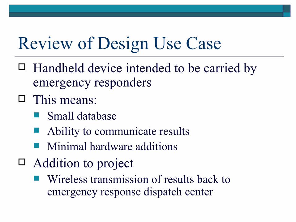
BLOSUM62: Design Investigation Options
1. Program one of the processors to find neighbor words and run b62_score
2. Implement neighbor_words and the BLOSUM62 matrix on the FPGA in custom hardware

Algorithm Analysis Finding
BLOSUM62 value clearly has the largest impact on BLASTP
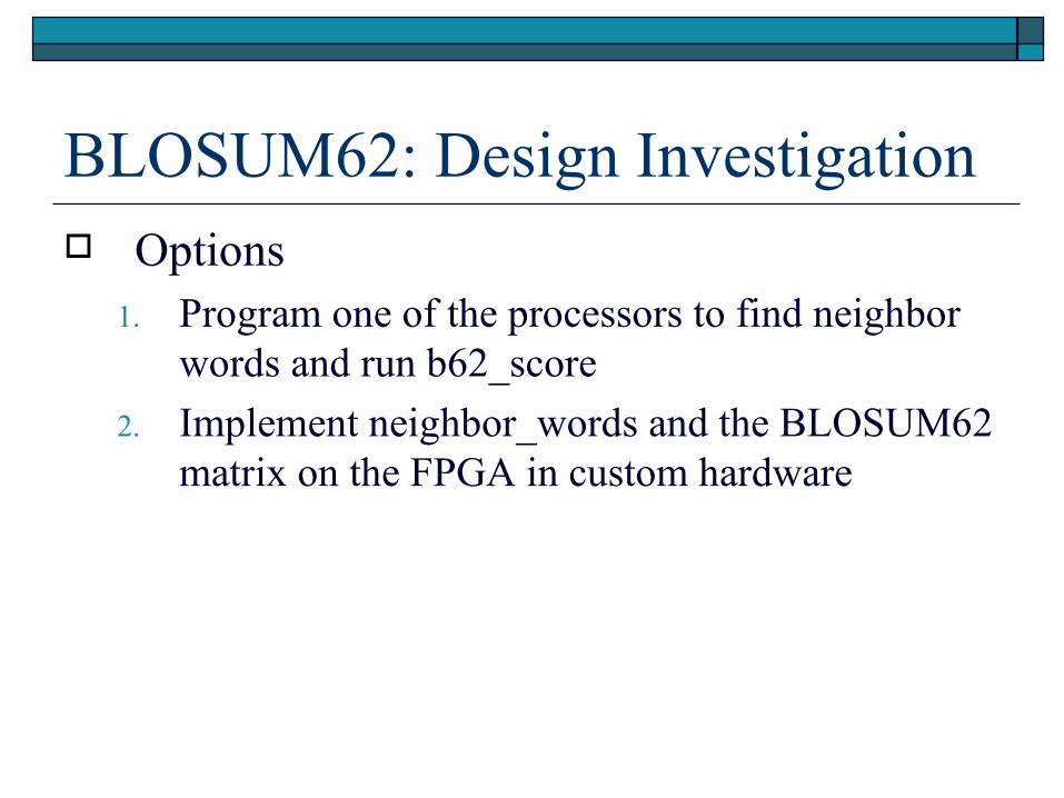
Pros/Cons Option 1 – Processor
Pro: Much easier to implement Con: Even with algorithm improvements there is unlikely
to be large improvements in run time of this portion Option 2 – Custom Hardware
Con: More complicated to implement, timing more of a problem
Pro: Much faster runtime, even when using the same algorithm
Either way, only limited improvements possible for a look-up table
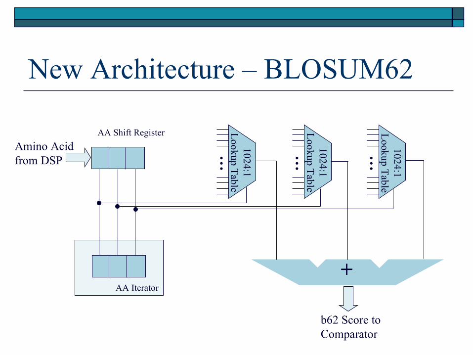
New Architecture – BLOSUM62
AA Iterator
AA Shift Register
… … …
+
Amino Acid from DSP
b62 Score to Comparator
1024:1 L
ookup Table
1024:1 L
ookup Table
1024:1 L
ookup Table

BLOSUM62 FPGA usage lookup_table (one B62 table)
0/8,320 logic elements (0% ) 4,096/106,496 memory bits (3.8%)
top_blossum 142/8,320 logic elements (1.7%) 12,288/106,496 memory bits (11.5%)

BLOSUM62 Runtime Timing requirements
Longest delay - 28.408ns Max clock frequency - 34.48 MHz
Estimated runtime of example Analysis of 25 character Amino Acid sequence
Approx. 25*243 = 345,600 clock cycles
Estimated run time of example sequence 345,600 * 1/35MHz = 9.87ms
Apples-to-oranges comparison, but... clearly much faster then previously

Database Exploration Initially considered using NIOS as memory
controller for two-level hierarchy Bring database chunks in from the Ethernet board Store them to the flash Use SRAM as buffer to serve requests while flash
was writing NIOS Ethernet controller uses too many pins
Couldn’t use memory and Ethernet Needed new design
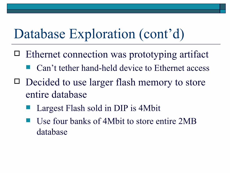
Database Exploration (cont’d) Ethernet connection was prototyping artifact
Can’t tether hand-held device to Ethernet access
Decided to use larger flash memory to store entire database Largest Flash sold in DIP is 4Mbit Use four banks of 4Mbit to store entire 2MB
database

Database Exploration (cont’d) Lower 19 bits of address sent to all banks Upper 2 bits of address will be decoded to act
as chip-enable signals Allows 8-bit data busses to be tied together Doesn’t require additional tri-state buffers
Fall-back plan If hardware is uncooperative, revert to 2Mbit
Flash chip for Demo 2

DSP Exploration The DSP is complicated! Major piece of work is A/D conversion and
processing the signal with interrupts DSP Demo lecture last week was a big help
Did lots of review to refresh interrupt programming
Nucleotide to Amino Acid conversion DSP or Custom Hardware? DSP is easier to code and speed is not a big factor for this
stage

DSPFPGA Interface How to send Amino Acids Only 4 bits for output from DSP!
Send most frequent Amino Acids encoded in few bits in one handshake
If not one of most frequent, another handshake is needed to specify which one it is
This speeds up transmission from the DSP to the FPGA Custom Hardware

ARM and BLASTP ARM contains three MATLAB functions
extend_hit find_hsps find_seeds
Interfaces FPGA - input from custom hardware FPGA - output to NIOS processor flash controller AVR - output for terminal driver and for TNC

ARM and BLASTP String Matching
Haven’t really done much exploration or full implementation with this yet
ARM is middle point in architecture Starting from DSP and Flash moving inwards

Holy crap! We’re way behind! Work on TNC has been shifted to lower
priority to allow more focus on core work (BLASTP algorithm)
Molly has functioned as contract engineer to Daniel and Lisa Helped plan new memory system Helped Lisa with b62_score strategery, beat
Cadence into shape, re-learned Verilog

Hardware vs. Software TNC Option #1: Hardware-based TNC
Use second ATmega8 as basis More realistic prototype for design use case FSK requires more complex EE knowledge
Analog circuits make Molly have nightmares
Option #2: Software-based TNC Windows sound card driver Requires second sound card on TX end

Saved by the Internet!
But, we don’t want APRS... Get to simplify this quite a bit, luckily Must write drivers for our wireless protocol,
transmission Lots of ATmega8 fun in Molly’s future
(http://www.knology.net/~gdion/whereavr.html)

Inputs to TNC Terminal AVR acts as serialization for
wireless TNC Less stress on ARM
7
ATmega8(for terminal)
ATmega8(TNC)
To TX/RX

So... how do we encode data? Frequency Shift Keying
(FSK) Digital frequency
modulation where modulating signal shifts output frequency between two discrete values: “mark” and “space”
Audio Frequency Shift Keying (AFSK) “Mark” and “space”
frequencies are tones in audio range
(http://searchnetworking.techtarget.com/WhatIs/images/fsk.gif)
OK, how do we send packets? AX.25 Amateur Packet-Radio
Data Link Layer Protocol OSI layers 1 and 2 Similar to wireless Ethernet
Derived from X.25 but w/o third layer Supports connected and connectionless transfer Error detecting (but no FEC)
Order of Approach Most “important” (or at least, 545-ish) part of
this is the wireless protocol implemented on the AVR
Will do this part first on digital level Get protocol working in 1’s and 0’s in standard C Then, port to AVR
Worry about oscillators, FSK, actually keying transceiver last

Obligatory Legalese Amateur frequencies have stringent requirements for
station identification; all comms must be 2-way Precautions:
TNC will ID both sender and receiver with each packet transmitted
On startup, transmit explanation of what’s to follow, refer questions to simplex phone frequency monitored during demo
(Lastly, clearing our conscience should we ever put this presentation online...) Please refer all questions to KD8AKT, KG4ZEX
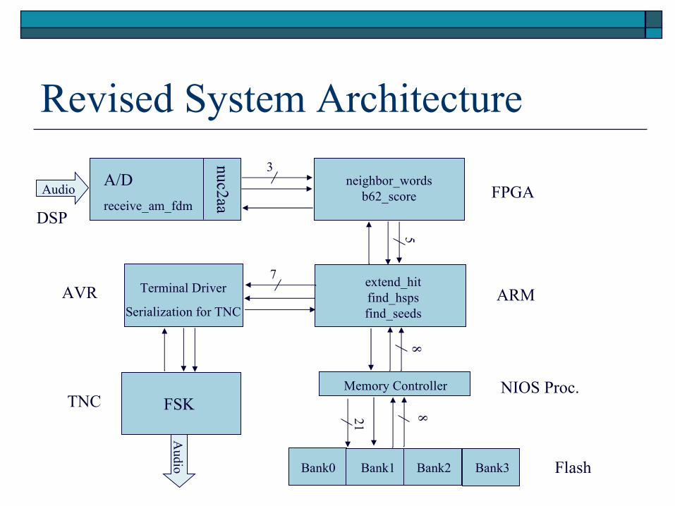
Revised System Architecture
DSP
A/D
receive_am_fdm
nuc2aa
neighbor_wordsb62_score
3
5
FPGA
ARMextend_hitfind_hspsfind_seeds
8
NIOS Proc.Memory Controller
FlashBank0 Bank1 Bank2 Bank3
21
8
7Terminal Driver
Serialization for TNCAVR
TNC FSK
Audio
Audio
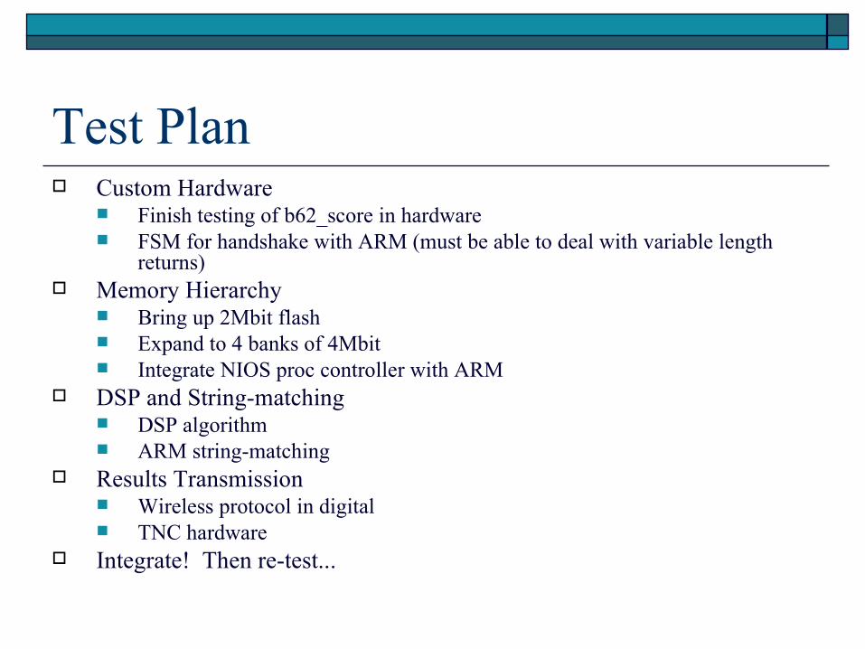
Test Plan Custom Hardware
Finish testing of b62_score in hardware FSM for handshake with ARM (must be able to deal with variable length
returns) Memory Hierarchy
Bring up 2Mbit flash Expand to 4 banks of 4Mbit Integrate NIOS proc controller with ARM
DSP and String-matching DSP algorithm ARM string-matching
Results Transmission Wireless protocol in digital TNC hardware
Integrate! Then re-test...
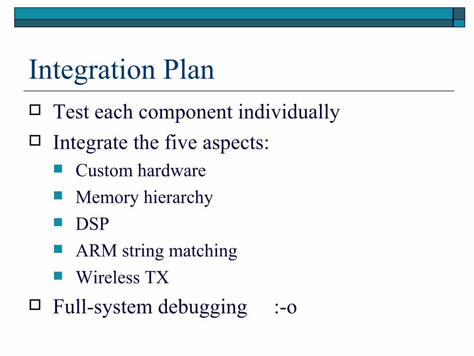
Integration Plan Test each component individually Integrate the five aspects:
Custom hardware Memory hierarchy DSP ARM string matching Wireless TX
Full-system debugging :-o

Demo #2 DSP
A/D conversion and nuc2aa Communicate results to FPGA
Custom Hardware Handles amino acids to custom hardware to neighbor words Communicate results to ARM All working in synthesizable behavioral Verilog
Memory 16Mbit array working and responding to NIOS proc (2Mbit flash if
hardware not arrived) Serving requests to ARM
Wireless Wireless protocol in C working on digital level (1’s and 0’s, not AFSK)

Demo #3
Everything works! Full functionality of all components Successful communication of data to transfer from
the original wave on the sound card, through virus detection, and back to another sound card via wireless transmission
Can we graduate now?
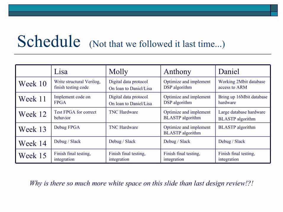
Schedule (Not that we followed it last time...)
Finish final testing, integration
Finish final testing, integration
Finish final testing, integration
Finish final testing, integrationWeek 15
Debug / SlackDebug / SlackDebug / SlackDebug / SlackWeek 14
BLASTP algorithmOptimize and implement BLASTP algorithm
TNC HardwareDebug FPGAWeek 13
Large database hardware
BLASTP algorithm
Optimize and implement BLASTP algorithm
TNC HardwareTest FPGA for correct behaviorWeek 12
Bring up 16Mbit database hardware
Optimize and implement DSP algorithm
Digital data protocol
On loan to Daniel/Lisa
Implement code on FPGAWeek 11
Working 2Mbit database access to ARM
Optimize and implement DSP algorithm
Digital data protocol
On loan to Daniel/Lisa
Write structural Verilog, finish testing codeWeek 10
DanielAnthonyMollyLisa
Why is there so much more white space on this slide than last design review!?!
Lessons Learned Sometimes it’s easier to make Perl write Verilog for
you (1024:1 mux is one of these times) Check if power is connected to all components! Strings of variable length and the FPGA don’t mix
well Spring Break is fatal to our work ethic If half your group leaves a file called Pinouts.txt on
the desktop, the rest of your group should read it before wiring the breadboard (We love you, Lisa!)
Questions??