Area Efficient low power FFT design using CSLA and vedic multiplier
International Journal of Research and Scientific Innovation (IJRSI) | Volume IV, Issue XII, December 2017 | ISSN 2321–2705
www.rsisinternational.org Page 18
Design of Low Power Binary Multiplier
K. Madhuri1, C.Bhargav
2, T.Chakrapani
3, K .Sudhakar
4
1MTECH VLSI, Dept of ECE, ST.Johns College of Engineering and Technology, Kurnool, Andhra Pradesh, India.
2Assistant Professor, Dept of ECE, ST.Johns College of Engineering and Technology, Kurnool, Andhra Pradesh, India.
3Associate Professor, Dept of ECE, ST.Johns College of Engineering and Technology, Kurnool, Andhra Pradesh, India.
4H.O.D, Associate Professor, Dept of ECE, ST.Johns College of Engineering and Technology, Kurnool, Andhra Pradesh, India.
Abstract: In today’s world of electronics industries low power
has emerged as a principal theme. For integrated Chip, Power
dissipation has become an important consideration as
performance and area design. Due to increased complexity,
reducing power consumption and over all power management of
the IC are the key challenges. The need to reduce package cost
and extended battery life is emphasis for many designs along
with optimization of power and timing. Multipliers play a vital
role in the computation part of ALU. Binary multiplication by
digital circuits requires the generation of partial products,
addition of partial product by reduction tree until two partial
product rows remain and adding of partial product rows by an
adder. In this project a low power binary multiplier is designed
using voltage scaling technique.
Keywords: Multiplier, Power Dissipation, Voltage scaling, ALU
I. INTRODUCTION
multiplier is one of the key hardware blocks in most
digital and high performance systems such as FIR filters,
digital signal processors and microprocessors etc. With
advances in technology, many researchers have tried and are
trying to design multipliers which offer either of the
following- high speed, low power consumption, regularity of
layout and hence less area or even combination of them in
multiplier. Thus making them suitable for various high speed,
low power, and compact VLSI implementations. However
area and speed are two conflicting constraints. So improving
speed results always in larger areas. So here we try to find out
the best trade off solution among the both of them. Generally
as we know multiplication goes in two basic steps. Partial
product and then addition. Hence in this project we have first
tried to design different adders and compare their speed and
complexity of circuit i.e. the area occupied. And then we have
designed the Binary multiplier.
II. MOTIVATION
As the scale of integration keeps growing, more and more
sophisticated signal processing systems are being
implemented on a VLSI chip. These signal processing
applications not only demand great computation capacity but
also consume considerable amount of energy. While
performance and Area remain to be the two major design tolls,
power consumption has become a critical concern in today’s
VLSI system design. The need for low-power VLSI system
arises from two main forces. First, with the steady growth of
operating frequency and processing capacity per chip, large
currents have to be delivered and the heat due to large power
consumption must be removed by proper cooling techniques.
Second, battery life in portable electronic devices is limited.
Low power design directly leads to prolonged operation time
in these portable devices. Multiplication is a fundamental
operation in most signal processing algorithms. Multipliers
have large area, long latency and consume considerable
power. Therefore low-power multiplier design has been an
important part in low- power VLSI system design. There has
been extensive work on low-power multipliers at technology,
physical, circuit and logic levels. A system’s performance is
generally determined by the performance of the multiplier
because the multiplier is generally the slowest element in the
system. Furthermore, it is generally the most area consuming.
Hence, optimizing the speed and area of the multiplier is a
major design issue. However, area and speed are usually
conflicting constraints so that improving speed results mostly
in larger areas. As a result, a whole spectrum of multipliers
with different area- speed constraints has been designed with
fully parallel. Fully Parallel Multipliers at one end of the
spectrum and fully serial multipliers at the other end. In
between are digit serial multipliers where single digits
consisting of several bits are operated on. These multipliers
have moderate performance in both speed and area. However,
existing digit serial multipliers have been plagued by
complicated switching systems and/or irregularities in design.
Radix 2^n multipliers which operate on digits in a parallel
fashion instead of bits bring the pipelining to the digit level
and avoid most of’ the above problems. These structures are
iterative and modular. The pipelining done at the digit level
brings the benefit of constant operation speed irrespective of
the size of’ the multiplier. The clock speed is only determined
by the digit size which is already fixed before the design is
implemented.
Multiplication consists of three steps: generation of partial
products or (PPG), reduction of partial products (PPR), and
finally carry-propagate addition (CPA).In general there are
sequential and combinational multiplier implementations. We
only consider combinational case here because the scale of
integration now is large enough to accept parallel multiplier
implementations in digital VLSI systems. Different
multiplication algorithms vary in the approaches of PPG,
PPR, and CPA. For PPG, radix-2 is the easiest. To reduce the
number of PPs and consequently reduce the area/delay of PP
A
International Journal of Research and Scientific Innovation (IJRSI) | Volume IV, Issue XII, December 2017 | ISSN 2321–2705
www.rsisinternational.org Page 19
reduction, one operand is usually recoded into high-radix digit
sets. The most popular one is the radix-4 digit set {-2,-1, 0, 1,
2}. For PPR, two alternatives exist: reduction by rows ,
performed by an array of adders, and reduction by columns,
performed by an array of counters. The final CPA requires a
fast adder scheme because it is on the critical path. In some
cases, final CPA is postponed if it is advantageous to keep
redundant results from PPG for further arithmetic operations
Multipliers are the key components in the data path which
consume huge amount of power and occupy large areas. In
multipliers, the power dissipation is huge owing to the power
dissipated in the large number of gates which are a part of the
multiplier structure. Adder blocks form the building blocks for
various multiplier structures. In general, any multiplication
operation can be divided into three steps [6]
1) Partial Product Generation – With the inputs available
generating partial products utilizing a collection of gates.
2) Partial Product Reduction – Utilizing the adders to reduce
the partial products to sum and carry vectors for further
computation.
3) Final Carry-Propagate Addition – Adding sum and carry
vectors to produce the final result.
A multiplication operation performed on an M-bit number and
an N-bit number results in a result with (M + N) number of
bits. The figure below shows a basic scheme for an unsigned
M x N-bit multiplier [12]
In general, multipliers can be classified in three broad
categories [12]
1) Sequential Multipliers – in these types of multipliers, the
partial products are generated sequentially and these are added
to the previously accumulated sum. The shift and add
multipliers are an example of sequential multipliers. The delay
of sequential multipliers is very large and so hardly put into
use in modern designs.
2) Parallel Multipliers – in these types of multipliers, the
partial products are generated in parallel and multi operand
fast adders are used for accumulation of the product.
3) Array Multipliers – these types of multipliers iteratively
utilize identical cells that generate new partial products and
accumulate them simultaneously.
A multiplier is one of the key hardware blocks in most digital
signal processing (DSP) systems. Typical DSP applications
where a multiplier plays an important role include digital
filtering, digital communications and spectral analysis
(Ayman.A et al (2001)). Many current DSP applications are
targeted at portable, battery-operated systems, so that power
dissipation becomes one of the primary design constraints.
Since multipliers are rather complex circuits and must
typically operate at a high system clock rate, reducing the
delay of a multiplier is an essential part of satisfying the
overall design.
III. IMPLEMENTATION
BINARY MULTIPLIER
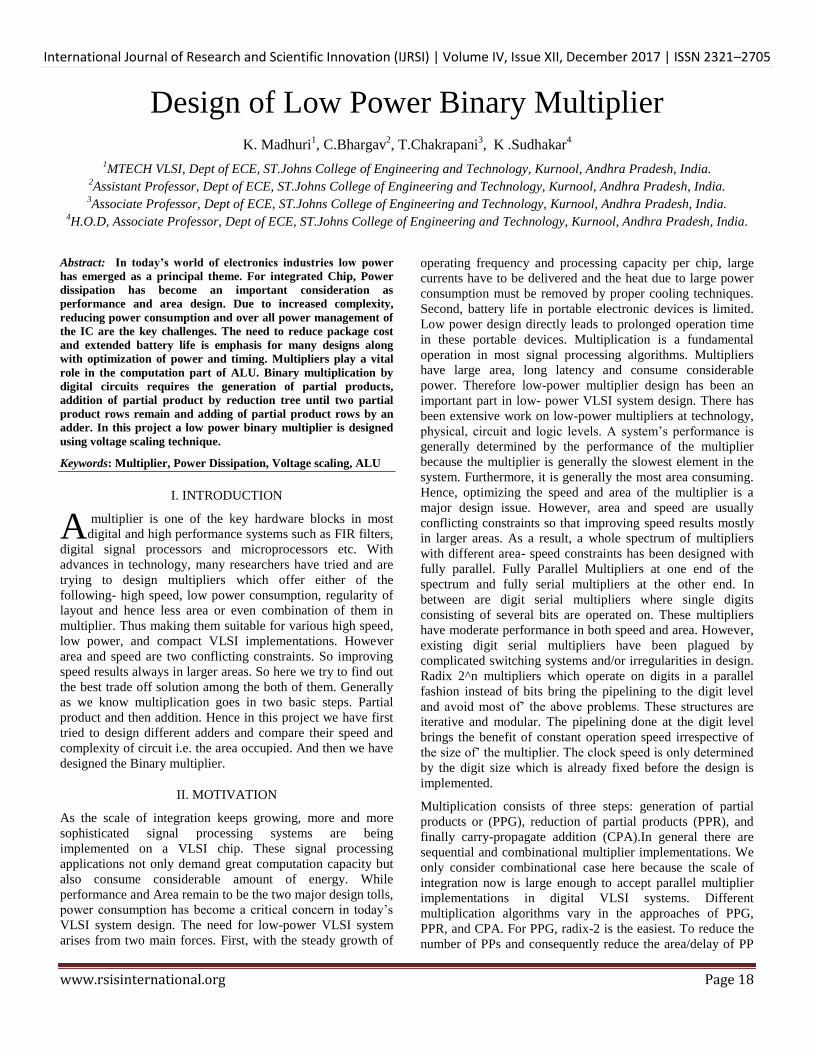
Figure 1: Schematic of 4bit-binary multiplier
Figure 1a: Schematic of 4bit-binary multiplier with inputs
Figure 1b: Timing diagramof 4bit-binary multiplier
International Journal of Research and Scientific Innovation (IJRSI) | Volume IV, Issue XII, December 2017 | ISSN 2321–2705
www.rsisinternational.org Page 20
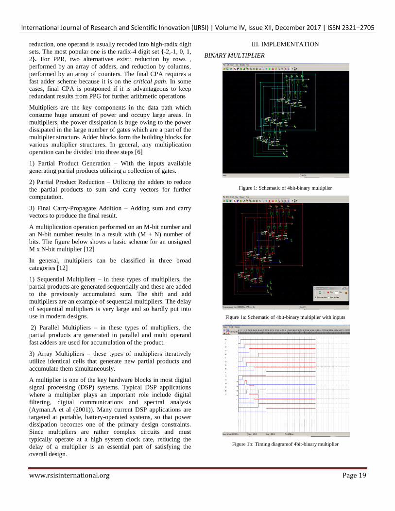
Figure 1c: Layout diagram of 4bit-binary multiplier
Figure 1d: Power dissipation diagram of 4bit-binary multiplier
REVERSIBLE BINARY MULTIPLIER
Figure 2: Schematic of 4bit-Reversible binary multiplier
Figure 2a: Timing Diagram of 4bit-Reversible binary multiplier
Figure 2b: Timing Diagram of 4bit-Reversible binary multiplier
Figure 2c: Layout Diagram of 4bit-Reversible binary multiplier
Figure 2d: Power dissipation diagram of 4bit- Reversible binary multiplier
Figure 3: Schematic of MBE
International Journal of Research and Scientific Innovation (IJRSI) | Volume IV, Issue XII, December 2017 | ISSN 2321–2705
www.rsisinternational.org Page 21
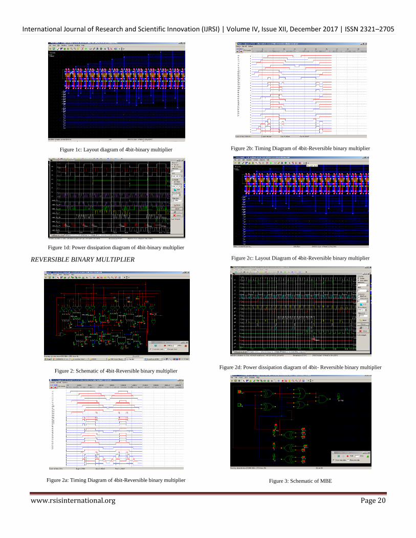
Figure 3a: Timing Diagram of MBE
Figure 3b: Layout of MBE
Figure 3c: Power Dissipation of MBE in 120µm technology
Figure 3d: Power Dissipation of MBE in 90nm technology
Figure 4 : Schematic of Partial Product generator Q18+& Q19+
Figure 4a: Timing Diagram of Partial Product generator Q18+& Q19+
Figure 4b: Layout Diagram of Partial Product generator Q18+& Q19+
Figure 4c: Power Dissipation Diagram of Partial Product generator Q18+ &
Q19+
International Journal of Research and Scientific Innovation (IJRSI) | Volume IV, Issue XII, December 2017 | ISSN 2321–2705
www.rsisinternational.org Page 22
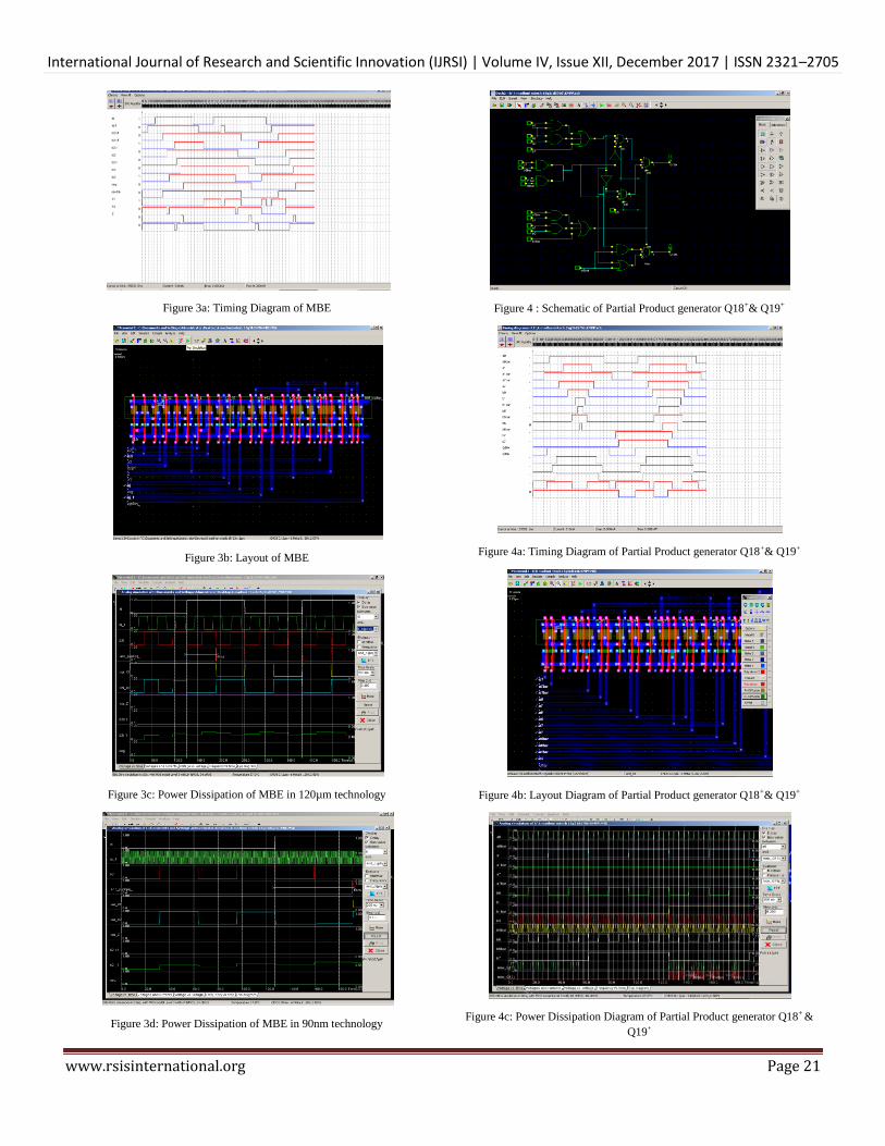
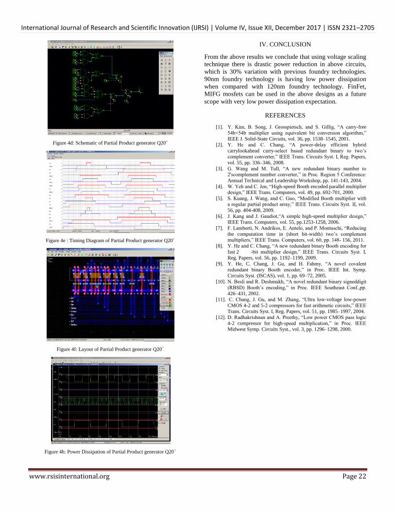
Figure 4d: Schematic of Partial Product generator Q20+
Figure 4e : Timing Diagram of Partial Product generator Q20+
Figure 4f: Layout of Partial Product generator Q20+
Figure 4h: Power Dissipation of Partial Product generator Q20+
IV. CONCLUSION
From the above results we conclude that using voltage scaling
technique there is drastic power reduction in above circuits,
which is 30% variation with previous foundry technologies.
90nm foundry technology is having low power dissipation
when compared with 120nm foundry technology. FinFet,
MIFG mosfets can be used in the above designs as a future
scope with very low power dissipation expectation.
REFERENCES
[1]. Y. Kim, B. Song, J. Grosspietsch, and S. Gillig, “A carry-free
54b×54b multiplier using equivalent bit conversion algorithm,” IEEE J. Solid-State Circuits, vol. 36, pp. 1538–1545, 2001.
[2]. Y. He and C. Chang, “A power-delay efficient hybrid
carrylookahead carry-select based redundant binary to two’s complement converter,” IEEE Trans. Circuits Syst. I, Reg. Papers,
vol. 55, pp. 336–346, 2008.
[3]. G. Wang and M. Tull, “A new redundant binary number to 2'scomplement number converter,” in Proc. Region 5 Conference:
Annual Technical and Leadership Workshop, pp. 141-143, 2004.
[4]. W. Yeh and C. Jen, “High-speed Booth encoded parallel multiplier design,” IEEE Trans. Computers, vol. 49, pp. 692-701, 2000.
[5]. S. Kuang, J. Wang, and C. Guo, “Modified Booth multiplier with a regular partial product array,” IEEE Trans. Circuits Syst. II, vol.
56, pp. 404-408, 2009.
[6]. J. Kang and J. Gaudiot,“A simple high-speed multiplier design,” IEEE Trans. Computers, vol. 55, pp.1253-1258, 2006.
[7]. F. Lamberti, N. Andrikos, E. Antelo, and P. Montuschi, “Reducing
the computation time in (short bit-width) two’s complement multipliers,” IEEE Trans. Computers, vol. 60, pp. 148- 156, 2011.
[8]. Y. He and C. Chang, “A new redundant binary Booth encoding for
fast 2 -bit multiplier design,” IEEE Trans. Circuits Syst. I, Reg. Papers, vol. 56, pp. 1192–1199, 2009.
[9]. Y. He, C. Chang, J. Gu, and H. Fahmy, “A novel covalent
redundant binary Booth encoder,” in Proc. IEEE Int. Symp. Circuits Syst. (ISCAS), vol. 1, pp. 69–72, 2005.
[10]. N. Besli and R. Deshmukh, “A novel redundant binary signeddigit
(RBSD) Booth’s encoding,” in Proc. IEEE Southeast Conf.,pp. 426–431, 2002.
[11]. C. Chang, J. Gu, and M. Zhang, “Ultra low-voltage low-power
CMOS 4-2 and 5-2 compressors for fast arithmetic circuits,” IEEE Trans. Circuits Syst. I, Reg. Papers, vol. 51, pp. 1985–1997, 2004.
[12]. D. Radhakrishnan and A. Preethy, “Low power CMOS pass logic
4-2 compressor for high-speed multiplication,” in Proc. IEEE Midwest Symp. Circuits Syst., vol. 3, pp. 1296–1298, 2000.