Design of Low Power Column Bypass Multiplier using FPGA ...
4
Copyright © 2013 IJECCE, All right reserved 1571 International Journal of Electronics Communication and Computer Engineering Volume 4, Issue 5, ISSN (Online): 2249–071X, ISSN (Print): 2278–4209 Design of Low Power Column Bypass Multiplier using FPGA and Implementation Using FIR Filter Vemula Prakash Department of ECE, Malla Reddy Engg College (Autonomous)-Hyderabad Email: [email protected] Mekala Rama Rao Department of ECE, Malla Reddy Engg College (Autonomous)-Hyderabad Email: [email protected] Dr. M. Ch. P. Jagdissh Department of ECE, Malla Reddy Engg College (Autonomous)-Hyderabad Email: [email protected] Abstract – Design of area, high speed and power efficient data path logic systems in the low power VLSI circuits has been identified as vital technology in the in the DSP computations and signal processing applications like FIR,IIR filters. Since multipliers consume most of the power in DSP computations it is very important to develop new low-power multipliers for DSP computations. The switching activity of the multiplier depends on the input bit-coefficient, if the coefficient bits are zero the corresponding rows or columns need not to be activated. By inserting more number of zeros in the multiplicand using booth recoding unit we can reduce the switching activity by shutting down the idle part of the circuit and thereby reducing the power dissipation, based on this concept we presents low power column bypass multiplier and verifies the result using FIR filter. Keywords – Power Efficient, Switching Activity, Column Bypass. I. INTRODUCTION Multiplication is an essential arithmetic operation in DSP computations. For the multiplication of two unsigned n-bit numbers, the multiplicand, A = an-1 an-2 . . . a0, and the multiplier, B = bn-1 bn-2 . . . b0, the product, P = P2n-1P2n- 2. . . P0, can be represented as the following equation: Product (P): For achieving of high-execution speed in DSP computations, parallel array multiplier is widely used and the typical implementation of such an array multiplier is Braun design. In this paper, we presents low power Column bypass multiplier design methodology that inserts more number of zeros in the multiplicand thereby reducing the number of switching activities as well as power consumption. The switching activity of the multiplier depends on the input bit coefficient. This means if the input bit coefficient is zero, corresponding row or column of adders need not be activated. If multiplicand contains more zeros, higher power reduction can be achieved. To reduce the switching activity is to shut down the idle part of the circuit, which is not in operating condition. Low power adder structure reduces the activity of switching. Flexibility is another critical requirement that mandates the use of programmable components like FPGAs in such devices. As we get closer to the limits of scaling in Complementary metal, Oxide. Semiconductor (CMOS) circuits, area, speed and power dissipation issues are becoming more and more important. In recent years, the impact of pervasive computing and the internet have accomplished this trend. The applications for these domains are run on battery-powered embedded systems. The resultant constraints on the energy budget require design for power as well as design for performance at all layers of system design. Thus reducing power consumption is an important design achievement for portable computing and communication devices that employ increasingly sophisticated and power hungry signal processing techniques. Flexibility is another critical requirement that mandates the use of programmable components like FPGAs in such devices. As the multiplier bits increases the length of the process and also the complexity of the multiplication increases. For this reason research has begun for reducing the complexity as well as power consumption, the solution is if the input bit coefficient is ‘0’ the corresponding switching activity should be zero. Further we can bypass the power and multiplication process so that we can reduce the power. II. EXISTING DESIGNS A. BRAUN Multiplier The Braun multiplier removes the extra correction circuitry needed. Also, number of adders is less. But, it is limited to first row of adders the limitation of this technique is that it cannot stop the switching activity even if the bit coefficient is zero that results in unnecessary power dissipation. Another low power designs disable the operation in some rows, designed a technique that reduces the switching to fairly good extent. The Braun parallel multiplier operates by computing the partial products in parallel and by shifting and accumulating the partial products. The Switching activity is poor; it is correlated with the input coefficient. Particularly, reducing the switching activity of the component can minimize the power dissipation in the design. The limitation of this technique is that it cannot stop the switching activity even if the bit coefficient is zero that ultimately results in unnecessary time delay and power dissipation. Another design is required to overcome the problems of power dissipation and speed of execution.
Transcript of Design of Low Power Column Bypass Multiplier using FPGA ...

Copyright © 2013 IJECCE, All right reserved1571
International Journal of Electronics Communication and Computer EngineeringVolume 4, Issue 5, ISSN (Online): 2249–071X, ISSN (Print): 2278–4209
Design of Low Power Column Bypass Multiplier usingFPGA and Implementation Using FIR Filter
Vemula PrakashDepartment of ECE,
Malla Reddy Engg College(Autonomous)-Hyderabad
Email: [email protected]
Mekala Rama RaoDepartment of ECE,
Malla Reddy Engg College(Autonomous)-Hyderabad
Email: [email protected]
Dr. M. Ch. P. JagdisshDepartment of ECE,
Malla Reddy Engg College(Autonomous)-Hyderabad
Email: [email protected]
Abstract – Design of area, high speed and power efficientdata path logic systems in the low power VLSI circuits hasbeen identified as vital technology in the in the DSPcomputations and signal processing applications like FIR,IIRfilters. Since multipliers consume most of the power in DSPcomputations it is very important to develop new low-powermultipliers for DSP computations. The switching activity ofthe multiplier depends on the input bit-coefficient, if thecoefficient bits are zero the corresponding rows or columnsneed not to be activated. By inserting more number of zerosin the multiplicand using booth recoding unit we can reducethe switching activity by shutting down the idle part of thecircuit and thereby reducing the power dissipation, based onthis concept we presents low power column bypass multiplierand verifies the result using FIR filter.
Keywords – Power Efficient, Switching Activity, ColumnBypass.
I. INTRODUCTION
Multiplication is an essential arithmetic operation inDSP computations. For the multiplication of two unsignedn-bit numbers, the multiplicand, A = an-1 an-2 . . . a0, andthe multiplier, B = bn-1 bn-2 . . . b0, the product, P =P2n-1P2n- 2. . . P0, can be represented as the followingequation:Product (P):
For achieving of high-execution speed in DSPcomputations, parallel array multiplier is widely used andthe typical implementation of such an array multiplier isBraun design.
In this paper, we presents low power Column bypassmultiplier design methodology that inserts more number ofzeros in the multiplicand thereby reducing the number ofswitching activities as well as power consumption. Theswitching activity of the multiplier depends on the inputbit coefficient. This means if the input bit coefficient iszero, corresponding row or column of adders need not beactivated. If multiplicand contains more zeros, higherpower reduction can be achieved. To reduce the switchingactivity is to shut down the idle part of the circuit, which isnot in operating condition. Low power adder structurereduces the activity of switching. Flexibility isanother critical requirement that mandates the use ofprogrammable components like FPGAs in such devices.
As we get closer to the limits of scaling inComplementary metal, Oxide. Semiconductor (CMOS)circuits, area, speed and power dissipation issues arebecoming more and more important. In recent years, theimpact of pervasive computing and the internet haveaccomplished this trend. The applications for thesedomains are run on battery-powered embedded systems.The resultant constraints on the energy budget requiredesign for power as well as design for performance at alllayers of system design. Thus reducing powerconsumption is an important design achievement forportable computing and communication devices thatemploy increasingly sophisticated and power hungrysignal processing techniques. Flexibility is another criticalrequirement that mandates the use of programmablecomponents like FPGAs in such devices.
As the multiplier bits increases the length of the processand also the complexity of the multiplication increases.For this reason research has begun for reducing thecomplexity as well as power consumption, the solution isif the input bit coefficient is ‘0’ the correspondingswitching activity should be zero. Further we can bypassthe power and multiplication process so that we can reducethe power.
II. EXISTING DESIGNS
A. BRAUN MultiplierThe Braun multiplier removes the extra correction
circuitry needed. Also, number of adders is less. But, it islimited to first row of adders the limitation of thistechnique is that it cannot stop the switching activity evenif the bit coefficient is zero that results in unnecessarypower dissipation. Another low power designs disable theoperation in some rows, designed a technique that reducesthe switching to fairly good extent.
The Braun parallel multiplier operates by computing thepartial products in parallel and by shifting andaccumulating the partial products. The Switching activityis poor; it is correlated with the input coefficient.Particularly, reducing the switching activity of thecomponent can minimize the power dissipation in thedesign.
The limitation of this technique is that it cannot stop theswitching activity even if the bit coefficient is zero thatultimately results in unnecessary time delay and powerdissipation. Another design is required to overcome theproblems of power dissipation and speed of execution.
Copyright © 2013 IJECCE, All right reserved1572
International Journal of Electronics Communication and Computer EngineeringVolume 4, Issue 5, ISSN (Online): 2249–071X, ISSN (Print): 2278–4209
Fig.1. 4x4 block diagram of Braun Multiplier
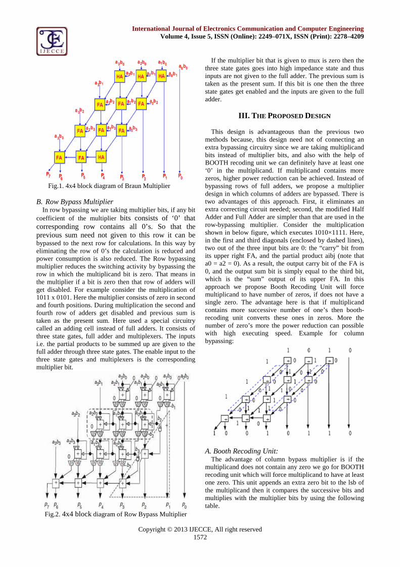
B. Row Bypass MultiplierIn row bypassing we are taking multiplier bits, if any bit
coefficient of the multiplier bits consists of ‘0’ thatcorresponding row contains all 0’s. So that theprevious sum need not given to this row it can bebypassed to the next row for calculations. In this way byeliminating the row of 0’s the calculation is reduced andpower consumption is also reduced. The Row bypassingmultiplier reduces the switching activity by bypassing therow in which the multiplicand bit is zero. That means inthe multiplier if a bit is zero then that row of adders willget disabled. For example consider the multiplication of1011 x 0101. Here the multiplier consists of zero in secondand fourth positions. During multiplication the second andfourth row of adders get disabled and previous sum istaken as the present sum. Here used a special circuitrycalled an adding cell instead of full adders. It consists ofthree state gates, full adder and multiplexers. The inputsi.e. the partial products to be summed up are given to thefull adder through three state gates. The enable input to thethree state gates and multiplexers is the correspondingmultiplier bit.
Fig.2. 4x4 block diagram of Row Bypass Multiplier
If the multiplier bit that is given to mux is zero then thethree state gates goes into high impedance state and thusinputs are not given to the full adder. The previous sum istaken as the present sum. If this bit is one then the threestate gates get enabled and the inputs are given to the fulladder.
III. THE PROPOSED DESIGN
This design is advantageous than the previous twomethods because, this design need not of connecting anextra bypassing circuitry since we are taking multiplicandbits instead of multiplier bits, and also with the help ofBOOTH recoding unit we can definitely have at least one‘0’ in the multiplicand. If multiplicand contains morezeros, higher power reduction can be achieved. Instead ofbypassing rows of full adders, we propose a multiplierdesign in which columns of adders are bypassed. There istwo advantages of this approach. First, it eliminates anextra correcting circuit needed; second, the modified HalfAdder and Full Adder are simpler than that are used in therow-bypassing multiplier. Consider the multiplicationshown in below figure, which executes 1010×1111. Here,in the first and third diagonals (enclosed by dashed lines),two out of the three input bits are 0: the “carry” bit fromits upper right FA, and the partial product aibj (note thata0 = a2 = 0). As a result, the output carry bit of the FA is0, and the output sum bit is simply equal to the third bit,which is the “sum” output of its upper FA. In thisapproach we propose Booth Recoding Unit will forcemultiplicand to have number of zeros, if does not have asingle zero. The advantage here is that if multiplicandcontains more successive number of one’s then booth-recoding unit converts these ones in zeros. More thenumber of zero’s more the power reduction can possiblewith high executing speed. Example for columnbypassing:
A. Booth Recoding Unit:The advantage of column bypass multiplier is if the
multiplicand does not contain any zero we go for BOOTHrecoding unit which will force multiplicand to have at leastone zero. This unit appends an extra zero bit to the lsb ofthe multiplicand then it compares the successive bits andmultiplies with the multiplier bits by using the followingtable.

Copyright © 2013 IJECCE, All right reserved1573
International Journal of Electronics Communication and Computer EngineeringVolume 4, Issue 5, ISSN (Online): 2249–071X, ISSN (Print): 2278–4209
Table1: Booth Recoding TableMultiplicand Multiplier selected by
bit iBit i Bit i-10 0 0xM0 1 +1xM1 0 -1xM1 1 0xM
B. Design of Column Bypass MultiplierThe column bypassing multiplier is constructed as
follows. First, the modified HA cell is shown in figure. Ifaj = 0, the HA will be disabled. For a Braun multiplier,there are only two inputs for each FA in the first row (i.e.,row 0). Therefore, when aj = 0, the two input of FA0,j aredisabled, and thus it output carry bit will not be changed.Therefore, all three inputs of FA1,j are fixed, whichprohibit its output from changing.
Fig.3. (a): Modified Full \Adder (b): Modified Half Adder
Figure shows the 4x4 low power multiplier structure.This technique will be very useful as we go for higherwidth of the multiplicand specially when there aresuccessive numbers of ones. If multiplicand contain atleast one zero, it does not uses the Booth recoding unit andif Multiplicand is “11” then only it will use Boothrecoding table shown in table . So we do not need sign bitcircuitry. In this paper we have presented a newmethodology for designing of low power parallelmultiplier with reduced switching.
Fig.4. A 4x4 Column Bypass Multiplier
Method for increasing number of zeros in themultiplicand is discussed with the help of Booth RecodingUnit. Based on the modification of the half adders insteadof full adders in an array multiplier, a low-powermultiplier design column bypassing using Booth recodingis proposed. Compared with the row bypassing or array-multipliers, the experimental results show that ourproposed low-power multiplier achieves higher powerreduction with lower hardware overhead.
IV. EXPERIMENTAL RESULTS
For calculating performance of low power columnbypass multiplier we have taken FIR filter as anapplication in which we used array multiplier and columnbypass for MAC (multiply and accumulate unit) toexamine the xpower calculation to prove how much thepower can be reduced by this new multiplication methodon sparten 2S30 FPGA and the design is synthesized onXilinx 9.2i, synthesized results on Xilinx are shown belowin table2, simulation results for the proposed design shownin figure5.
Table 2: Synthesis results using FIR filter on XilinxCharacteristics Array
MultiplierProposedDesign
Power dissipation 91mW 87mWEstimated delay 7.89ns 5.20%No of LUTs 31% 44%Device Spartan 2 Spartan 2
Fig.5. Simulation results for the proposed design usingFIR filter
V. CONCLUSION
We can conclude that by using this technology, we canhave control over the three parameters AREA, POWERand SPEED with reduced switching activity. With the helpof BOOTH recoding unit, which will force to have at leastone zero in the multiplicand, we proposed low powerColumn bypass multiplier design methodology for highspeed and higher power reduction.

Copyright © 2013 IJECCE, All right reserved1574
International Journal of Electronics Communication and Computer EngineeringVolume 4, Issue 5, ISSN (Online): 2249–071X, ISSN (Print): 2278–4209
REFERENCES
[1] A. Wu, .High performance adder cell for low power pipelinedmultiplier., in Proc. IEEE Int. Symp. On Circuits and systems,May 1996,vol.4,pp.57-60.
[2] Hichem Belhadj, Behrooz Zahiri, Albert Tai .Power-sensitivedesign techniques on FPGA devices., Proceedings ofinternational conference on IC Taipai(2003).
[3] Oscal T.-c.Chen, sandy Wang, and Yi-Wen Wu, .Minimizationof Switching Activities of Partial Products for Designing Low-Power Multipliers, IEEE Transactions on VLSI systems, june2003 vol.11,no.3.
[4] Rajendra M.Patrikar, K. Murali, Li Er Ping,. Thermaldistribution calculations for block level placement in theembedded systems., Microelectronics Reliability44(2004) 129-134.
AUTHOR’S PROFILE
V. PrakashPursuing final year M.Tech with the specialization ofdigital systems &computer electronics in thedepartment of ECE in Malla Reddy EngineeringCollege-Hyderabad, India. He completed his B.Tech inSIND Ramagundam. His interests are in VLSI andEmbedded Systems.
Mekala Rama Raois working as an Assistant Professor in the departmentof ECE in Malla Reddy Engg College-Hyderabad,India. He is having 9 years of teaching experience inVLSI and Digital Electronics. His areas of interests areVLSI, Digital Electronics and Digital SignalProcessing.
Dr. M. C. J. Prasadis presently working as a head of the Department ofECE, MREC, Hyderabad, India. He is having 15 yearsof teaching experience. His areas of interests arecommunication systems, digital systems, imageprocessing, digital signal processing, advanced DSPsystems.

![FPGA Implementation of 8-bit Multiplier with Reduced Delay ...ijcce.org/papers/270-E075.pdf · Based on performance comparison [5], [6], array multiplier is selected for the purpose](https://static.fdocuments.net/doc/165x107/5aeaccd57f8b9a66258c87f2/fpga-implementation-of-8-bit-multiplier-with-reduced-delay-ijcceorgpapers270-e075pdfbased.jpg)