Brent CarlsonEVLA System PDR (Correlator V2) December 4-5, 2001 1 Correlator.

.
DESIGN APPROACH FOR A MICROPROCESSOR-BASED GPS TIME TRANSFER RECEIVER
P.C. Ould and R.J. Van Wechel, Interstate Electronics Corporation,
Anaheim, California
ABSTRACT
This paper describes the design concept and charac- teristics of a self-contained microprocessor-based GPS time transfer receiver. is currently in the test phase. digital baseband correlation rather than analog IF correlation of the signals with the reference code. The correlator, numerically controlled oscillators (NCO) and code generator are implemented in a special-purpose digital signal processor. time is recovered in the digital code tracking loop, and final corrections are applied in the control pro- cessor. By means of asynchronous samding techniques for the digital correlator and NCO, the time transfer resolution limit is 2’N part of a code chip period, where N is 32 for a 32-bit accumulator in the MCO. Other features of this design are: drift-free dig- ital mechanization, high reliability of digital cir- cuits, flexible control capability of the micropro- cessor, and potential for a high degree of digital VLSI chip development leading to compact, low-cost units e
A prototype of this unit It employs two-bit
The
A description is given of the process by which the precise measurement is made between user clock and received signal code. times in the code tracking loop yield high-resolution uncorrected time sample words. These uncorrected time words are corrected for range to the satellite, satellite clock error, ionospheric error, and relativistic errors. They are then differenced with the user clock to yield user-clock error estimates.
The user-clock-derived sample
User-clock outputs consist of 1-pps, time readout, and direct digital outputs of time and time error of the user clock.
Test data on random error of the approach are also presented.
373
https://ntrs.nasa.gov/search.jsp?R=19820012638 2020-04-30T12:01:02+00:00Z

.
INTRODUCTION
The GPS rece iver described i n t h i s paper cons i s t s of a baseband RF converter, d i g i t a l s i g n a l processor, and general-purpose microprocessor. The design approach and components have been developed a t I n t e r s t a t e Elec t ronics during t h e p a s t four years as p a r t of an i n t e r n a l l y funded GPS app l i ca t ions research program. The goal of t h i s research e f f o r t is t o develop a r e l i a b l e , low-cost, and highly accura te modular system t h a t can be configured t o s a t i s f y a wide range of requirements i n t h e areas of timing, tracking, and navigation.
Our design approach is pr imar i ly d i g i t a l i n t h a t t h e received s i g n a l is converted t o baseband and d i g i t i z e d before any signal processing is attempted. the la tes t gate-array and custom-VLSI (Reference 1) techniques. System accuracy i s achieved through use of d i g i t a l c o r r e l a t i o n techniques (Reference 2) with asynchronous sampling t o a t t a i n very high measure- ment reso lu t ion , and by using long ( i . e . , 32-bit) word lengths.
W e intend t o achieve r e l i a b i l i t y and low cos t by employing
This paper emphasizes t h e c h a r a c t e r i s t i c s of t h e d i g i t a l s i g n a l pro- cessor t h a t provide t h e c a p a b i l i t y of ex t r ac t ing t i m e from the received s i g n a l d i r e c t l y as a numerical. value.
Evaluation of t h i s GPS t i m e t r a n s f e r technique is cu r ren t ly i n progress a t I n t e r s t a t e , and t h e r e s u l t s of i n i t i a l tests of t h e system's t racking accuracy are included i n t h e paper.
BACKGROUND
Our work with GPS rece ive r s began i n t h e middle of t h e last decade with development of t h e F l i g h t T e s t Support System (FTSS) f o r t h e Navy's Trident I (C4) s t r a t e g i c weapon system (Reference 3 ) . The FTSS employed the e a r l y GPS satellites f o r m e t r i c ( pos t f l i gh t ana lys i s ) t racking and t i m e d iv i s ion mul t ip l e access (TDMA), pseudorandom-noise (PRN)-coded ground transmissions f o r range s a f e t y tracking. Many of t h e d i g i t a l - baseband processing techniques we are now using f o r GPS processing or ig ina ted i n t h e FTSS.
W e subsequently developed a breadboard GPS system t h a t w a s used f o r test and eva lua t ion a t our f a c i l i t y about two years ago. system employed c l ea r / acqu i s i t i on (C/A)-code, one-bit d i g i t a l baseband co r re l a t ion and w a s an a l l - d i g i t a l system (Reference 2) except f o r t h e RF converter, which converted t h e received signal t o baseband f o r d i g i t i z a t i o n . lrlent Corporation PDP-11 computer.
This GPS rece iv ing
The system's c e n t r a l processing u n i t w a s a D i g i t a l Equip-
The t i m e t r a n s f e r receiver described here is a microprocessor-based system using a Motorola Corporation MC68000 as its c e n t r a l processing
374

. u n i t . P-code c a p a b i l i t y added t o determine and compare t h e time-transfer accuracy and r e l i a b i l i t y achievable with each code, and t o s a t i s f y requirements f o r o ther appl ica t ions .
This vers ion is a combined C/A- and P-code GPS receiver, with t h e
GEWERAL DESCRIPTION
Figure 1 is a func t iona l block diagram of the GPS t i m e t r a n s f e r receiver. The RF converter is a s t ra ight forward , double-conversion device f o r L1. The carrier numerically cont ro l led o s c i l l a t o r (NCO) d r ives t h e baseband converter t o tune t h e receiver t o the s i g n a l p lus Doppler. (The s t ruc- t u r e of t h i s second-order phaselocked loop i s described l a t e r . ) The d i g i t i z e r (Figure 1) has been mechanized as e i t h e r a one- o r two-bit (Reference 2 ) analog-to-digital converter sampling a t a rate s l i g h t l y higher than t w i c e t h e code ch ip rate.
The c o r r e l a t o r processes t h e d i g i t i z e d in-phase (I) and quadrature (Q) da t a t o generate a tracking-error s igna l . t rack ing e r r o r , t h e delay t racking f i l t e r d r ives t h e code NCO and code generator. more d e t a i l with the c lock and i t s associated components).
The in t eg ra t ed c o r r e l a t i o n d a t a and loop feedback s igna l s are sampled a t 250 Hz.
I n response t o t h e delay
This loop is t h e t i m e t r a n s f e r mechanism (described later i n
In our system, t h e microprocessor accomplishes most of t h e s i g n a l processing. Figure 2 i l l u s t r a t e s the algorithms and process flow. Nofe t h a t t h e code generator is mechanized i n a sepa ra t e microprocessor (Reference 2) and t h a t bas i c s i g n a l acqu i s i t i on is not shown.
A l l computations except clock co r rec t ion are completed i n less than 4 milliseconds. bas i s .
Clock co r rec t ion operates continuously on a p r i o r i t y
CARRIER AND CODE TRACKING
Figure 3 shows the bas ic operation of t h e c a r r i e r and code t racking loops.
I n acqu i s i t i on , t h e carrier NCO and code generator are operated i n a search p a t t e r n t h a t r e s u l t s i n a co r re l a t ion function being centered i n t h e early/on-time/late c o r r e l a t o r output. complex (I and Q) outputs are used f o r carrier tracking, and an estimate of t h e angle of t hese c o e f f i c i e n t s y i e l d s t h e carrier-loop phase e r r o r . This is analogous t o conventional Costas-loop carrier tracking. carrier-loop e r r o r is f i l t e r e d i n the loop f i l t e r f o r second-order carrier-loop tracking. The carrier frequency estimate con t ro l s t h e
The on-time c o r r e l a t o r
The
375

.
carrier NCO and a l s o is sca led t o c o n t r o l t h e code NCO frequency, and t o provide dynamic a id ing f o r the f i r s t -o rde r code t racking loop.
The code loop der ives i t s delay e r r o r s i g n a l from t h e d i f f e rence of t h e magnitudes of t h e e a r l y and late co r re l a t ion coe f f i c i en t s , i n t h e manner of a noncoherent code t racking loop. The code loop is f i r s t -o rde r , with a id ing from the c a r r i e r loop, and con t ro l s t h e delay of t h e code NCO/ code generator d i r e c t l y r a t h e r than t h e more usual process of con t ro l l - ing t h e code ch ip frequency. This con t ro l mechanism o f f e r s some s i g n i f i c a n t advantages i n achieving very-high-resolution time t r a n s f e r measurement.
BASIC APPROACH TO TIME TRANSFER
Figure 4 i s a func t iona l block diagram of t h e GPS t i m e t r a n s f e r process, t he bas i c element of which is t h e code t r ack loop t h a t keeps a l o c a l re ference code synchronously t racking t h e received code. phase o r t i m e de lay of t h e re ference code is cont ro l led a t t h e start of each loop i t e r a t i o n ( 4 milliseconds) by t h e feedback from t h e code loop f i l t e r . The cont ro l word from t h e loop f i l t e r is s p l i t i n t o in t ege r and f r a c t i o n a l p a r t s i n terms of code chip un i t s ; t h e in t ege r p a r t sets t h e s t a r t i n g ch ip number of t h e code generator, and t h e f r a c t i o n a l p a r t sets the s t a r t i n g phase of t h e NCO.
The i n i t i a l
This con t ro l mechanism f o r t he combined NCO/code generator is very p rec i se and eliminates t h e need f o r a high-resolution t i m e i n t e r v a l counter t o perform the bas ic t i m e d i f fe rence measurement between re fer - ence t i m e and received code epochs. Figure 5 i l l u s t r a t e s how the 43-bit i n t ege r delay sets t h e s t a r t i n g code chip, and a 32-bit con t ro l word i n i t i a l i z e s t h e NCO s t a r t i n g phase. This, i n e f f e c t , sets the s t a r t i n g phase t o a r e so lu t ion of 2-N p a r t of a code chip, where N i s 32 f o r a 32-bit accumulator i n the NCO.
Figure 6 ou t l ines t h e form of t h e NCO f o r t h i s process. The NCO con- sists of an accumulator r e g i s t e r t h a t can be p re se t by the f r a c t i o n a l chip phase command word from t h e code loop f i l t e r whenever each loop f i l t e r i t e r a t i o n begins. The frequency command word i s then added t o the accumulator on each clock t i m e , causing t h e accumulator t o overflow a t an average frequency equal t o the des i red chip frequency. It i s important i n t h i s process t o maintain a n asynchronous r e l a t ionsh ip between t h e NCO output frequency and t h e NCO accumulation rate over the e n t i r e Doppler range. s i g n i f i c a n t b i t (MSB) from t h e accumulator needs t o be used as an NCO output, and i t then advances t h e code generator a ch ip on each overflow of t h e NCO accumulator.
When t h i s i s done, i t is found t h a t only t h e most
376

.
Although it may appear at first that such a code generation process would yield unacceptably high jitter in the code loop, this has not been the case, because of the broad spectral distribution of the NCO phase jitter. We use the same process in the carrier and code loops and see a phase jitter of about 2 degrees r m s (for high-SNR signals) in the carrier track loop, as shown in Figure 7. Code track results are shown in Figure 8, which is a time history of the combined code NCO/code generator control words plotted for an actual satellite pass. No smoothing was used on the plotted data, in order to illustrate the resolution of the raw delay measurements.
Referring again to Figure 4, it can be observed that the nominal 4- millisecond loop iteration rate of the code loop is derived from the user clock. On each 4-millisecond loop iteration, an uiicorrected time word in units of integer and fractional code chips is extracted from the code loop. This time word consists of the raw uncorrected time measure- nents that can be corrected for range, ionospheric error, relativistic error, satellite clock error, etc. They can be used as measurement values input to a Kalman filter to model various systematic and random clock errors. User clock error is determined by differencing with the user clock value at the same iteration time mark. The clock can be set to null the error by a combination of setting the clock counter in 200-nanosecond increments and, in finer increments, by phase control of the reference frequency input. Note (Figure 4 ) that uncorrected time measurements have a different significance, depending on whether the tracking mode is C/A- or P-code. In the P-code mode, the code state represents the time of the week (TOW) in direct unambiguous form. In the C/A-code mode, the TOW establishment and maintenance is somewhat less direct in that it involves a combination of measured C/A delay and resolution of the 1-millisecond C/A-code ambiguity.
DESIGN APPROACH
The components of the signal processor described in Figure 1 are designed to interface with the Motorola VERSAbus*. Figure 9 shows the particular configuration used for the P-code time transfer processor.
The VERSAbus concept provides a dedicated section for the microprocessor functions and a user-definable section.
The microprocessor bus supports a multiprocessor system that can be used to support auxiliary processors for navigation, clock error estimation, and special-purpose 1/0 and display functions.
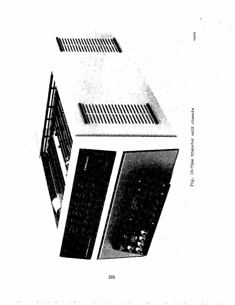
Figure 10 is a photograph of the enclosure for this design. circuit boards, which have the physical characteristics- of a Motorola MORmacs* board, are shown in Figures 11 and 12. The RF converter is
Typical
*Begis t e r e d trademarks of Motor0 Za Co-rporation .
377

packaged i n a module so t h a t it plugs i n t o t h e enclosure i n t h e same manner as t h e processor boards. d i sk , and p r i n t e r i n add i t ion t o t h e bas i c con t ro l panel.
The present design includes a CRT,
This modular design approach provides extensive f l e x i b i l i t y t o def ine systems f o r custom appl ica t ions .
REFERENCES
1. C. Mead and L. Conway, Introduction to VLSISys tems , Addison- Wesley Publishing Company, 1980.
2. P.C. Ould and R.J . Van Wechel, "All-Digital GPS Receiver Mechanization," Proceedings of the National Aerospace Meeting, The I n s t i t u t e of Navigation, 8-10 A p r i l 1981; a l s o t o appear i n Navigation, Vol. 28, No . 3, F a l l 1981.
3. T. Thompson, "Performance of t h e Satrack/Global Posit ioning System, Trident I Missile Tracking System," Proceedings of the 2980 IEEE Position, Location, and Navigation Symposium, pp. 445-449.
378

Control Panel
4
output Code Delay c Control
c
Compute Codestate Parameters
Microprocessor
Compute Clock Correction
I I ",'PPS Clock Error L - - - - - J Parallel/Serial lime of Day
I
Fig. 1-Functional block diagram of GPS t i m e t r a n s f e r receiver
*
Signal Poll Signal Processor
I
I input Data
Update Code loop
d
1 input Data Carrier loop
U
* Re-Entrant
Delay Control
Fig. 2-Process f low c h a r t Y 379

t-OLZEI
r! - c o x
X I 3
t t
m a 0 0 d
5 (d k U
aJ a 0 0
a 9 k aJ
.I4 k k (d r)
%I 0
g .rl U nf k aJ a 0
1 m
M .I4 Frr

. C-&Z&4J1
I - ‘ I N
r
381

.
I i
Hardware Software
I
c I N
3 a
Frodona1 Chip Code Deltry Command from CPU
Digital Code Command Frequency from CPU
Fig. 5-NCO/code generator control
Phase eommand Register 1 #
f Frequency Common$ 32-Bit Accumulator Register
t
Reference Code integral Chip Code Delay Command from CPU
Fig. 6-Code NCO function
382

TO - -
60 - -
50-7
40
30
4
- *
3
Phase Jitter (deg rms)
2
20--
lo--
1
Signa! Source - Simulator -10 dB SNR in 1 MHz
Error
:y-+L x Phase Jitter
0.0 1 0.1 1 .o 10.0 Phase-Lock-Loop Natural Frequency (HI)
Raw Time Detay
(Refative) (nrec)
Fig. 7- Measured phase jitter and random Doppler error vs loop bandwidth
0.1 D m N
0.001
WR =6.l nsec., 0.7-Hz Loop Bandwidth 1 1
, (withoutadd*ionalsmoothingf
I t I I t I I t
t I I I I I I I I 1 I I
I I
I f
~ , - - - - - - - - - - ' - - - - - - - - - - - - - - - - - - - - - - - - - - - I I I I I c g
Measured Delay vs Time I NAVSTAR4
I 10:35 a.m., PDT 27 June 1980
Back Side Pass r
I t I I 1 I t I I I I I I t I I t I I I I I I I I t
t
I I I I t I I I _ _ _ _ _ _ _ _ _ _ _ _ _ _ _ _ _ - _ - - - - - - - - - - - - - - - - - - - - 0 0.625 1.25 2.5 3.75
Time (sec) Fig. 8-Typical time-delay measurement test results
I f I
I I
I t
I I
t
I I I I E
I I
I I I
I I t
I I t
I I . k:;. I
"'b k: I
383

.
L
384
r
38 5
?! m to r

Fig. l l -Cor re l a to r p r in t ed -c i r cu i t board
Fig. 12-Code generator p r in t ed -c i r cu i t board
386