DESIGN AND REALIZATION OF MICROSTRIP LINEAR ANTENNA ARRAY...
106
DESIGN AND REALIZATION OF MICROSTRIP LINEAR ANTENNA ARRAY BASED ON SIW (SUBSTRATE INTEGRATED WAVEGUIDE) FEED NETWORK A THESIS SUBMITTED TO THE GRADUATE SCHOOL OF NATURAL AND APPLIED SCIENCES OF MIDDLE EAST TECHNICAL UNIVERSITY BY ALİ ÖZGÜN IN PARTIAL FULLFILLMENT OF THE REQUIREMENTS FOR THE DEGREE OF MASTER OF SCIENCE IN ELECTRICAL AND ELECTRONICS ENGINEERING JULY 2014
Transcript of DESIGN AND REALIZATION OF MICROSTRIP LINEAR ANTENNA ARRAY...

DESIGN AND REALIZATION OF MICROSTRIP LINEAR ANTENNA
ARRAY BASED ON SIW (SUBSTRATE INTEGRATED WAVEGUIDE)
FEED NETWORK
A THESIS SUBMITTED TO
THE GRADUATE SCHOOL OF NATURAL AND APPLIED SCIENCES
OF
MIDDLE EAST TECHNICAL UNIVERSITY
BY
ALİ ÖZGÜN
IN PARTIAL FULLFILLMENT OF THE REQUIREMENTS
FOR
THE DEGREE OF MASTER OF SCIENCE
IN
ELECTRICAL AND ELECTRONICS ENGINEERING
JULY 2014

Approval of the thesis:
DESIGN AND REALIZATION OF MICROSTRIP LINEAR ANTENNA
ARRAY BASED ON SIW (SUBSTRATE INTEGRATED WAVEGUIDE)
FEED NETWORK
submitted by ALİ ÖZGÜN in partial fulfillment of the requirements for the degree
of Master of Science in Electrical and Electronics Engineering Department,
Middle East Technical University by,
Prof. Dr. Canan Özgen
Dean, Graduate School of Natural and Applied Sciences _________________
Prof. Dr. Gönül Turhan Sayan
Head of Department, Electrical and Electronics Eng. _________________
Prof. Dr. Şimşek Demir
Supervisor, Electrical and Electronics Eng. Dept., METU _________________
Examining Committee Members:
Prof. Dr. Canan Toker
Electrical and Electronics Eng. Dept., METU _________________
Prof. Dr. Şimşek Demir
Electrical and Electronics Eng. Dept., METU _________________
Prof. Dr. Gönül Turhan Sayan
Electrical and Electronics Eng. Dept., METU _________________
Prof. Dr. Özlem Aydın Çivi
Electrical and Electronics Eng. Dept., METU _________________
Arslan Hakan Coşkun, Ph.D.
Lead Design Engineer, ASELSAN _________________
Date: 22/07/2014

iv
I hereby declare that all information in this document has been obtained
and presented in accordance with academic rules and ethical conduct. I also
declare that, as required by these rules and conduct, I have fully cited and
referenced all material and results that are not original to this work.
Name, Last name : Ali ÖZGÜN
Signature :

v
ABSTRACT
DESIGN AND REALIZATION OF MICROSTRIP LINEAR ANTENNA
ARRAY BASED ON SIW (SUBSTRATE INTEGRATED WAVEGUIDE)
FEED NETWORK
ÖZGÜN, Ali
M. Sc., Department of Electrical and Electronics Engineering
Supervisor: Prof. Dr. Şimşek Demir
July 2014, 90 pages
A microstrip patch antenna array with substrate integrated waveguide (SIW)
feed network is designed and realized. With this configuration, waveguide which
is advantageous in high frequency designs is integrated to antenna array in planar
form by eliminating the drawback of the bulky structure of them. The design is
based on an E-plane SIW power divider in multilayer form. For the feed network,
a 4-way E-plane SIW power divider is constituted with 3-layered structure and
an antenna system is obtained by merging the antenna layer with this 3-layered
feed network. Through this multilayer feed network, resultant antenna system
has a compact structure which is not enlarged by the feeding part. The developed
network has comparable performance with microstrip counterparts and it is more
advantageous for higher frequencies due to the planar waveguide structure.
Through the realization of the design, TRL calibration technique is applied to
extract the effects of the non-SIW parts from the measurement results.
Keywords: Substrate Integrated Waveguide (SIW), Antenna Array Feed
Network, E-Plane Power Divider, Patch Antenna, TRL Calibration

vi
ÖZ
SIW (SUBSTRATE INTEGRATED WAVEGUIDE) BESLEMELİ
MİKROŞERİT LİNEER ANTEN DİZİSİ AĞININ TASARIMI VE
GERÇEKLEŞTİRİLMESİ
ÖZGÜN, Ali
Yüksek Lisans, Elektrik ve Elektronik Mühendisliği Bölümü
Tez Yöneticisi: Prof. Dr. Şimşek Demir
Temmuz 2014, 90 sayfa
Taban malzemeye bütünleşik dalga kılavuzu (TMBDK) beslemeli mikroşerit
yama anten dizisi tasarlanmış ve gerçekleştirilmiştir. Bu sayede, yüksek frekans
tasarımlarında avantajlı olan dalga kılavuzu yapısı üç boyutlu şeklinden
kaynaklanan dezavantajından arındırılarak düzlemsel formda anten dizisine
entegre edilmiştir. Tasarım çok katmanlı E-plane TMBDK güç bölücü yapısını
temel almaktadır. Besleme devresi için 3 katmanlı E-plane TMBDK 4’e bölücü
oluşturulmuş ve anten katı bu 3 katmanlı yapıyla birleştirilerek anten sistemi
elde edilmiştir. Bu çok katmanlı besleme ağı sayesinde oluşturulan anten sistemi,
besleme kısmı tarafından boyutları genişletilmeden kompakt bir yapıya sahip
olmuştur. Geliştirilen ağ mikroşerit muadilleriyle karşılaştırılabilir performansa
sahiptir ve daha yüksek frekanslarda dalga kılavuzu yapısından kaynaklı olarak
daha da avantajlı durumdadır. Tasarımın gerçekleştirilmesi sırasında TMBDK
yapıya sahip olmayan yardımcı kısımların ölçüm sonuçlarından çıkartılması için
TRL kalibrasyon tekniği kullanılmıştır.
Anahtar Kelimeler: Taban Malzemeye Bütünleşik Dalga Kılavuzu (TMBDK),
Anten Dizisi Besleme Ağı, E-Plane Güç Bölücü, Yama Anten, TRL Kalibrasyon

vii
Burcum’a,

viii
ACKNOWLEDGEMENTS
Foremost, I would like to express my sincere gratitude to my advisor Prof. Dr.
Şimşek Demir who has supported me continuously with his motivation and
immense knowledge.
Besides my advisor, I would like to thank the thesis committee: Prof. Dr. Canan
Toker, Prof. Dr. Gönül Turhan Sayan, Prof. Dr. Özlem Aydın Çivi, and Dr.
Arslan Hakan Coşkun for their insightful comments and questions.
I also thank ASELSAN Inc. for the facilities provided in the production of the
materials during the study. I am also thankful to the staff Ömer Öcal, Murat
Sertkaya and others in the laboratory of ASELSAN for helping me with this
production process. My research would not have been possible without their
helps.
I am grateful to my friends, Muharrem Keskin and Akın Dalkılıç, for their
support throughout the development and the improvement of this thesis.
I thank my dearest friends Begüm Aytaç, Ayşe Dinçer and Ahmet Burak Aktaş
for the times we spend together. I also would like to thank my best friends Murat
Akpınar, Savaş Karadağ and Emre Başpınar for their endless support and
understanding throughout my life.
I also thank my mom, dad and sister for their valuable support despite the
distance between us.
Above all, I thank my wife Burcu Özgün for her peerless support throughout my
life and I am grateful to every moment she stand by me.

ix
TABLE OF CONTENTS
ABSTRACT ....................................................................................................... v
ÖZ ...................................................................................................................... vi
ACKNOWLEDGEMENTS ............................................................................ viii
LIST OF TABLES ............................................................................................ xi
LIST OF FIGURES .......................................................................................... xii
LIST OF ABBREVIATIONS ......................................................................... xvi
CHAPTERS
1. INTRODUCTION .......................................................................................... 1
1.1. Review of the Literature ...................................................................... 1
1.2. Organization of the Thesis ................................................................... 8
2. SIW THRU LINE DESIGN ......................................................................... 11
2.1. Design Parameters ............................................................................. 11
2.2. Microstrip-to-SIW Transition and Thru Line Design ........................ 14
2.3. Equivalency between SIW and Rectangular Waveguide .................. 22
2.4. TRL Calibration of SIW .................................................................... 23
3. E-PLANE SIW POWER DIVIDER DESIGN ............................................. 25
3.1. Layer-to-Layer Transition ................................................................. 26
3.2. Matching ............................................................................................ 29
3.3. 2-way Divider Design ........................................................................ 32
3.4. 4-way Divider Design ........................................................................ 35
4. ANTENNA ARRAY WITH SIW FEED NETWORK DESIGN ................ 41

x
4.1. Aperture Coupled Patch Antenna ...................................................... 41
4.2. Array Design with SIW Feed Network .............................................. 50
5. FABRICATION OF THE DESIGNS AND MEASUREMENT RESULTS 61
5.1. Fabrication of the Thru Line and Calibration Standards ................... 61
5.2. Fabrication of the 2-Way and 4-Way Dividers .................................. 67
5.3. Fabrication of the Patch Antenna Array with SIW Feed Network .... 78
6. CONCLUSIONS AND FUTURE STUDIES .............................................. 85
REFERENCES ................................................................................................. 87

xi
LIST OF TABLES
TABLES
Table 2-1: Optimization costs .......................................................................... 17
Table 4-1: Optimized patch dimensions for 60 mil RO4003 material ............. 45
Table 4-2: Optimized patch dimensions for 125 mil RT5880 material ........... 48

xii
LIST OF FIGURES
FIGURES
Figure 1-1: Basic SIW Structure [3] ................................................................... 2
Figure 1-2: Number of SIW papers published in IEEE in recent years [14] ...... 3
Figure 1-3 Six different non-planar SIC topologies: .......................................... 5
Figure 2-1: Leakage loss curves from 10-6 to 10-2 Np/rad with respect to distance
between the vias and their diameters normalized with the λc [17]. ................. 12
Figure 2-2: Suitable region for SIW design parameters [17]. .......................... 13
Figure 2-3: Simulation model for SIW on HFSS ............................................. 14
Figure 2-4: Microstrip taper for microstrip-to-SIW transition ......................... 15
Figure 2-5: Optimization results for the return loss of the thru line ................. 16
Figure 2-6: Optimization results for the insertion loss of the thru line ............ 16
Figure 2-7: SIW thru line design ...................................................................... 18
Figure 2-8: Field distribution of SIW thru line design ..................................... 18
Figure 2-9: Equivalent rectangular waveguide model for the SIW .................. 19
Figure 2-10: Field distribution of rectangular waveguide model ..................... 20
Figure 2-11: S-parameters for rectangular waveguide model of the thru line
design ................................................................................................................ 20
Figure 2-12: Characteristics of microstrip line which has same length with SIW
design ................................................................................................................ 21
Figure 2-13: Wide-band characteristics of SIW thru line ................................. 21
Figure 2-14: Comparison between SIW and rectangular waveguide models .. 23
Figure 2-15: TRL Standards ............................................................................. 24
Figure 2-16: TRL reference planes for TRL calibration .................................. 24
Figure 3-1: 3-D E-plane power divider design [32] ......................................... 25

xiii
Figure 3-2: Coupling slot between adjacent SIW layers .................................. 26
Figure 3-3: Field distribution around transition region .................................... 27
Figure 3-4: Coupling slot and termination sheet .............................................. 28
Figure 3-5: Multi-layer thru line design ........................................................... 29
Figure 3-6: Comparison between the single-layer and multi-layer thru lines .. 29
Figure 3-7: Initial design for the 2-way divider ............................................... 30
Figure 3-8: Top view of the 2-way divider layers ............................................ 30
Figure 3-9: Bottom view of the 2-way divider layers ...................................... 31
Figure 3-10: Stepped waveguide for transition region ..................................... 32
Figure 3-11: Comparison between straight and stepped dividers .................... 32
Figure 3-12: Field distribution of the 2-way divider ........................................ 33
Figure 3-13: 2-way SIW power divider characteristics .................................... 34
Figure 3-14: Amplitude and phase unbalance of the 2-way divider ................ 35
Figure 3-15: Top view of the 4-way divider layers .......................................... 36
Figure 3-16: Bottom view of the 4-way divider layers .................................... 37
Figure 3-17: Field distribution of the 4-way divider ........................................ 37
Figure 3-18: The 4-way SIW power divider characteristics ............................ 38
Figure 3-19: Amplitude unbalance of the 4-way divider ................................. 39
Figure 3-20: Phase unbalance of the4-way divider .......................................... 39
Figure 4-1: Design of the microstrip patch antenna ......................................... 42
Figure 4-2: Illustration of the coupling slot ...................................................... 43
Figure 4-3: Return loss performance of the patch antenna .............................. 43
Figure 4-4: Gain characteristic of the patch antenna ........................................ 44
Figure 4-5: Radiation pattern of the patch antenna .......................................... 44
Figure 4-6: Return loss performance of the patch antenna .............................. 46
Figure 4-7: Gain characteristic of the patch antenna ........................................ 46
Figure 4-8: Radiation pattern of the patch antenna .......................................... 47
Figure 4-9: Return loss performance of the patch antenna .............................. 48
Figure 4-10: Gain characteristic of the patch antenna ...................................... 49
Figure 4-11: Radiation pattern of the patch antenna ........................................ 49
Figure 4-12: Top view of the feed network and array design .......................... 51
Figure 4-13: Bottom view of the feed network and array design ..................... 52

xiv
Figure 4-14: Return loss performance of the patch antenna array ................... 53
Figure 4-15: Gain characteristic of the patch antenna array ............................. 53
Figure 4-16: Radiation pattern of the patch antenna array ............................... 54
Figure 4-17: Return loss performance of the patch antenna array ................... 55
Figure 4-18: Gain characteristic of the patch antenna array ............................. 55
Figure 4-19: Radiation pattern of the patch antenna array ............................... 56
Figure 4-20: Return loss performance of the patch antenna array ................... 57
Figure 4-21: Gain characteristic of the patch antenna array ............................. 57
Figure 4-22: Radiation pattern of the patch antenna array ............................... 58
Figure 4-23: Radiation pattern of the patch antenna array ............................... 59
Figure 4-24: Gain characteristic of the patch antenna array ............................. 59
Figure 5-1: Initial thru line design with solderable end launch connectors...... 62
Figure 5-2: Thru line design with 3 different configurations ........................... 63
Figure 5-3: Thru line design ............................................................................. 63
Figure 5-4: Insertion loss performance of the thru lines .................................. 64
Figure 5-5: Return loss performance of the thru lines ...................................... 64
Figure 5-6: Thru line design with slots ............................................................. 65
Figure 5-7: TRL calibration standards for both via and slot designs ............... 66
Figure 5-8: Calibration standards and measurement setup ............................... 66
Figure 5-9: Thru line characteristics with TRL calibration .............................. 67
Figure 5-10: Outer surfaces of the 2-way divider layers .................................. 68
Figure 5-11: Inner surfaces of the 2-way divider layers ................................... 68
Figure 5-12: 2-way divider layers with gel solder and insulator strip .............. 69
Figure 5-13: Comparison between soldered and solderless dividers ............... 69
Figure 5-14: Top view of the 2-way divider..................................................... 70
Figure 5-15: Bottom view of the 2-way divider ............................................... 70
Figure 5-16: Insertion loss performance of the 2-way dividers........................ 71
Figure 5-17: Return loss performance of the 2-way dividers ........................... 71
Figure 5-18: Measurement results of the 2-way divider with TRL calibration 72
Figure 5-19: Amplitude and phase unbalance of the 2-way divider................. 73
Figure 5-20: Outer surfaces and middle layer of the 4- way divider ................ 73
Figure 5-21: Inner surfaces and middle layer of the 4- way divider ................ 74

xv
Figure 5-22: Top view of the 4-way divider .................................................... 75
Figure 5-23: Bottom view of the 4-way divider ............................................... 75
Figure 5-24: Insertion loss characteristics of the 4-way divider ...................... 76
Figure 5-25: Return loss characteristics of the 4-way divider .......................... 76
Figure 5-26: Insertion loss characteristics of the 4-way divider with TRL
calibration ......................................................................................................... 77
Figure 5-27: Amplitude and phase unbalance of the 4-way divider ................ 77
Figure 5-28: Top view of the antenna array and feeding structure layers ........ 78
Figure 5-29: Bottom view of the antenna array and feeding structure layers .. 79
Figure 5-30: Top view of the antenna array network ....................................... 79
Figure 5-31: Bottom view of the antenna array network ................................. 80
Figure 5-32: Return Loss measurement of the Antenna Array ........................ 80
Figure 5-33: Satimo'sStarlab product [44] ....................................................... 81
Figure 5-34: The antenna placement and the measurement probes of the near
field measurement system ................................................................................ 82
Figure 5-35: Characteristics of the array gain for 8-10 GHz band ................... 83
Figure 5-36: Radiation patterns for the simulation and the measurement ....... 83

xvi
LIST OF ABBREVIATIONS
LTCC : Low Temperature Co-fired Ceramic
PCB : Printed Circuit Board
SIC : Substrate Integrated Circuits
SIW : Substrate Integrated Waveguide
SOLT : Short-Open-Line-Thru
TEM : Transverse Electromagnetic
TRL : Thru-Reflect-Line

1
CHAPTER 1
INTRODUCTION
1.1. Review of the Literature
With the development of new technologies and improvements upon the existing,
microwave and RF systems penetrated into many areas of both the daily life and
scientific studies. As this rapid development brings higher performance
requirements, for the high frequency system designs, being low-cost, high
quality, easy to produce and small in size emerges as the essential features.
Moreover, the printed circuit board technology has a widespread usage in such
systems, because planar structures are preferable in highly integrated designs.
In millimeter-wave technology, waveguides are more advantageous relative to
planar transmission lines due to their high quality factor and high power handling
performances. Furthermore, closed structure of waveguides which provides high
isolation and low radiation loss, increase its importance in millimeter-wave
systems which suffer from the interactions among the elements. Planar lines
have high conductor loss due to the high field density on the conductor edges,
while waveguides provide an advantage in this manner by providing low
conductor loss. However, high-cost and high-volume constitute significant
disadvantages to waveguides. Bulky structure of waveguides is probably the
weakest side in system development, because it is difficult to integrate bulky
components with planar structures.
2
Both planar and non-planar structures have significant disadvantages, thus
hybrid designs which merge the technologies with the aim of eliminating the
drawbacks, have become highly preferable in many applications. Besides this
advantage of the hybrid structures, they still have some drawbacks arising from
the transition between the planar and non-planar parts, especially in high
frequencies.
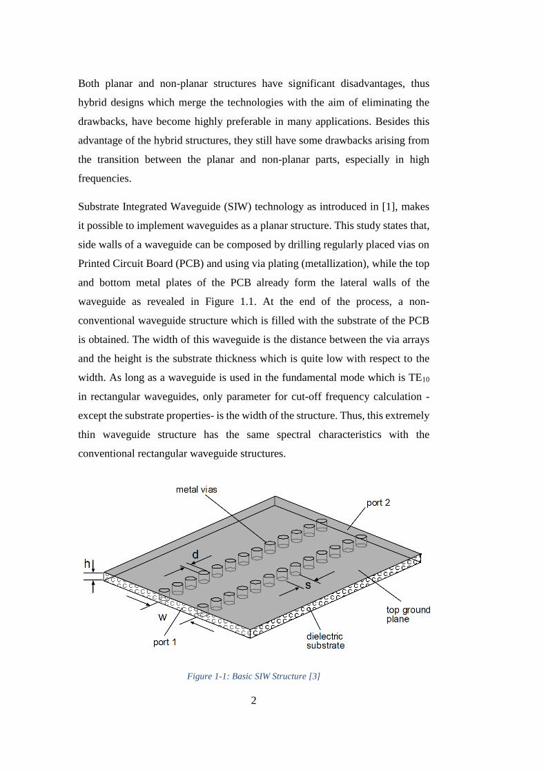
Substrate Integrated Waveguide (SIW) technology as introduced in [1], makes
it possible to implement waveguides as a planar structure. This study states that,
side walls of a waveguide can be composed by drilling regularly placed vias on
Printed Circuit Board (PCB) and using via plating (metallization), while the top
and bottom metal plates of the PCB already form the lateral walls of the
waveguide as revealed in Figure 1.1. At the end of the process, a non-
conventional waveguide structure which is filled with the substrate of the PCB
is obtained. The width of this waveguide is the distance between the via arrays
and the height is the substrate thickness which is quite low with respect to the
width. As long as a waveguide is used in the fundamental mode which is TE10
in rectangular waveguides, only parameter for cut-off frequency calculation -
except the substrate properties- is the width of the structure. Thus, this extremely
thin waveguide structure has the same spectral characteristics with the
conventional rectangular waveguide structures.
Figure 1-1: Basic SIW Structure [3]
3
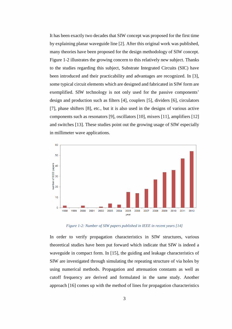
It has been exactly two decades that SIW concept was proposed for the first time
by explaining planar waveguide line [2]. After this original work was published,
many theories have been proposed for the design methodology of SIW concept.
Figure 1-2 illustrates the growing concern to this relatively new subject. Thanks
to the studies regarding this subject, Substrate Integrated Circuits (SIC) have
been introduced and their practicability and advantages are recognized. In [3],
some typical circuit elements which are designed and fabricated in SIW form are
exemplified. SIW technology is not only used for the passive components’
design and production such as filters [4], couplers [5], dividers [6], circulators
[7], phase shifters [8], etc., but it is also used in the designs of various active
components such as resonators [9], oscillators [10], mixers [11], amplifiers [12]
and switches [13]. These studies point out the growing usage of SIW especially
in millimeter wave applications.
Figure 1-2: Number of SIW papers published in IEEE in recent years [14]
In order to verify propagation characteristics in SIW structures, various
theoretical studies have been put forward which indicate that SIW is indeed a
waveguide in compact form. In [15], the guiding and leakage characteristics of
SIW are investigated through simulating the repeating structure of via holes by
using numerical methods. Propagation and attenuation constants as well as
cutoff frequency are derived and formulated in the same study. Another
approach [16] comes up with the method of lines for propagation characteristics

4
evaluation. This study together with [15] generates empirical formulations which
make the analysis and design steps straightforward like a conventional
waveguide design.
The main building block for SIW is periodic via arrays which determine the
performance of the design. For a well-designed SIW, rigid waveguide
formulations and derivations can be easily applied. Such a design is obtained
with the help of the derived design rules. In [17], a new method which is derived
from the concept of surface impedance calculation with the help of Method of
Moments (MoM) is presented for an accurately modeled SIW. The study
formulates propagation and leakage characteristics and determines the valid
region for the design parameters based on these formulations. The formulations
provide some rule of thumb for the basic parameters of SIW on which the whole
SIW design steps in this particular study effectively built.
In the last decade, SICs have found a large usage in high frequency designs for
the integration of planar and non-planar circuits. Structure of SICs varies
depending on the usage, and almost all kind of dielectric-filled waveguide types
can be generally implemented in SIC form by using metalized vias and air holes.
In general, any material-filled holes have usage in SIC designs [1]. Figure 1.3
illustrates some of the SIC types with the analogous planar waveguide structures
on top. Since it has a simple structure and is easy to produce, SIW is the most
popular one among SICs. In this study, SIW concept is used as a dielectric-filled
waveguide structure.

5
Figure 1-3 Six different non-planar SIC topologies: (a) Substrate Integrated Waveguide (SIW),
(b) Substrate Integrated Slab Waveguide (SISW), (c) Substrate Integrated Non-Radiating
Dielectric (SINRD) Guide, (d) Substrate Integrated Image Dielectric Guide (SIIDG), (e)
Substrate Integrated Inset Dielectric Guide (SIINDG), (f) Substrate Integrated Insular Guide
(SIIG). White disks stands for air hole, dark disks for metallized via and gray areas for dielectric
material. Dark rectangular parts are metal covers of dielectric material [1].
As SIW concept made it possible to use waveguide in planar structures, it is
appropriate to use it with other planar elements harmoniously. Besides SIW
design, a well-designed transition is also needed to provide this harmony. As
intended usage of SIW changes, different transmission types have been
produced. In [18], a rigid rectangular waveguide to SIW transition with 3-D
configuration is explained. The transition is realized with a single slot with
optimized dimensions. Another study [19] proposes a transition between coaxial
cables and SIW. In addition to these transition examples, the most interested one
is between microstrip and SIW. Majority of planar circuit elements are
compatible with microstrip lines and are generally linked to each other via this
type of lines. Basically, microstrip taper section, as initially proposed in [20] and

6
analyzed in detail in [21], is used for most of the transition designs. For this taper
design, firstly SIW impedance is calculated with equivalent waveguide model
and the transverse electromagnetic (TEM) waveguide model of the microstrip
part’s derivation followed. Lastly, parameters of the taper section with the help
of the analytical equations [22], are determined by using the impedances
calculated. In addition to microstrip transition, coplanar waveguide transition for
SIW usage is also applicable [23].
An equivalency can be obtained between SIW and conventional rectangular
waveguide based on their similar characteristics [24]. With this equivalency,
SIW structures are replaced by rectangular waveguides with no via for the
simulations. This replacement reduces the simulation cost drastically with an
insignificant change in the guiding characteristics. In this method, SIW design
begins with rectangular waveguide design with desired characteristics and then
the lateral walls of this rectangular waveguide is replaced by the SIW vias with
proper dimensions and positions as indicated in the equivalency equations.
Although the design of the transitions and the microstrip parts carry importance
for SIW structures, the most considerable importance is placed on the
performance of the SIW itself. To measure SIW design without microstrip parts,
TRL calibration is applied with designed calibration standards [25]. With TRL
calibration, effect of the microstrip parts is de-embedded from the measurement
results and SIW performance is obtained. Moreover, the transition design can be
verified by comparing data with and without TRL calibration.
Since SIW is a planar rectangular waveguide, waveguide power divider types
are also under the concern of SIW designers. Both T-junction and Y-junction
types of H-plane SIW power dividers are obtained with a single layer design [6].
Wilkinson power divider can also be implemented by inserting a resistive
element on SIW and thus waveguide divider can be used as a combiner [26]. Not
only H-plane but also E-plane dividers are implementable with SIW concept
[27], [28]. With the help of a vertical coupling slot between the SIW layers, this
E-plane division is realized with multilayer SIW structure. For E-plane divider,
number of divisions can be doubled by inserting an extra SIW layer. In [29], 4-

7
way E-plane divider design is proposed with 3-layered SIW structure. In addition
to these E-plane and H-plane power dividers, waveguide magic-T design with
SIW is proposed with [30] in which a planar magic-T is obtained with two-
layered SIW.
E-plane SIW dividers are multilayer structures due to the division principle. For
this multilayer design, a transition between adjacent layers is needed which is
applied for SIW lines in [31] with thin coupling slots and enriched by a 3-D from
in [32].Although these coupling slots and division process cause impedance
mismatch for both input and output, matching is obtained as explained in [29]
by adjusting and optimizing the SIW width near the transition section.
Since waveguides are important in antenna feeding networks due to their high
power handling and high frequency performances. As a planar type waveguide,
SIW is also preferred for antenna feeding. With SIW feed network, it is possible
to implement both waveguide feed network and antenna design on the same
substrate. In [33] and [34], quasi yagi antennas with SIW feeds are designed by
using a single substrate for both antennas and waveguide feed section. It is also
possible to construct multilayer SIW feed network with coupling slots between
the layers [35].
While aperture-coupled patch antennas are used widespread for multilayer
designs due to their advantages such as; spurious-free radiation, high radiation
efficiency and flexibility of choosing different substrates for the feed and the
antenna part as indicated in [36], some disadvantages of microstrip antennas are
given in [37]. The study emphasizes that these disadvantages can be removed or
decreased to some extent by applying certain techniques. Increasing the height
of the substrate and lowering the permittivity of the substrate on the antenna
layer to widen the antenna bandwidth are the two main proposals of the study.
Aperture coupled patch antennas are getting to be used widespread in SIW
applications. While in [38], a single microstrip patch antenna is fed by SIW line
for 60 GHz application, a 2x2 microstrip patch antenna array with SIW feed is
proposed in [39].

8
This study designs and demonstrates microstrip patch antenna array with SIW
feed network. Preparation for the final design is provided with the step by step
designing of the SIW feed network. Full-wave 3-D electromagnetic simulation
software HFSS© [40] is used for the entire electromagnetic simulation. After the
SIW thru line structure is put forward, design requirements for an efficient
transmission are investigated and SIW is validated by the fabricated designs. For
feed network, SIW power divider with E-plane configuration in multilayer form
is chosen. Through the design, the length and the width of the final design are
become equal to the patch array dimensions without feed network enlarging the
array dimensions by using multilayer design. With the aim of obtaining an
efficient feed network, 2-way and 4-way SIW dividers are designed and
produced. Following the optimizations with the 4-way divider, it is integrated
with the patch antenna array by replacing the microstrip division ports with the
coupling slots. This study contributes to SIW concept by proposing the usage of
multilayer E-plane SIW network for antenna array feeding which is a method
not touched upon by the previous studies.
1.2. Organization of the Thesis
Chapter 2 introduces the basic design stages of SIW and some rule of thumbs in
the literature are applied to SIW design. For the measurements of the design,
microstrip parts are inserted to the SIW section with the help of the transition
parts. This microstrip to SIW transition design is also given and equivalency
between SIW and rectangular waveguide is put forward. At the end of the
chapter TRL calibration for SIW line is explained.
Chapter 3 describes E-plane SIW power divider design. Having introduced the
transition between the SIW layers, impedance matching for divider design is
explained. After obtaining efficient division process on SIW, 2-way divider is
designed followed by 4-way divider design.

9
Chapter 4 explains the procedure for the formation of the microstrip patch
antenna array with the SIW feed network by using the 4-way divider design.
Following the design of the single aperture coupled patch antenna at the desired
frequency, patch and aperture dimensions are optimized with the simulations.
Using this single element antenna design, 4-element array is designed. For feed
network, 4-way SIW divider design is used by replacing microstrip output ports
with coupling apertures.
Chapter 5 illustrates the fabricated designs providing the measurements results.
Measurement results of the thru line, 2-way and 4-way divider designs are
compared with the simulation results. In the end, being the main purpose of this
study, 4-elements microstrip patch antenna array with E-plane SIW feed
network, is fabricated and measurements are presented.
Chapter 6 concludes and points out future study on this particular subject.


11
CHAPTER 2
SIW THRU LINE DESIGN
2.1. Design Parameters
Most of the properties of conventional rectangular waveguide such as
propagation characteristics, high quality-factor and high power-handling
remains in SIW structures. Some design rules are proposed in [17], in order to
preserve this analogy between SIW and non-planar metallic waveguide. As
revealed in Figure 1-1, main design parameters are the diameter 𝑑 of the vias,
the distance 𝑠 between the adjacent vias and the distance 𝑤 between the two
rows of vias. Furthermore, the substrate thickness and the permittivity of the
dielectric are the parameters to be chosen before the SIW design according to
the relevant usage and purpose of the design.
When constructing a SIW which guides the incoming wave like a rectangular
waveguide, first step is the decision for the via placement. With the help of [17],
a guided wave region on the 𝑑 𝑣𝑠. 𝑠 graph can be determined. As indicated in the
study, in order vias not to overlap, the distances between the vias should be
greater than the via diameter. This criterion is illustrated on 𝑑 vs. 𝑠 graph with
𝑑 = 𝑠 line and lower side of this line becomes forbidden region. Since the
distance 𝑠 mainly determines the leakage loss, it should be kept as small as
possible. Lower limit for 𝑠 is a fabrication concern as well as an issue about the
robustness of the thin structure. Via diameter 𝑑 has also impact on leakage loss

12
and it should be optimized with 𝑠. It is shown in [17] that the ratio 𝑠/𝑑 has a
direct relation with leakage loss and should be used as a design parameter. As
𝑠/𝑑 ratio increases, some of the energy inside the SIW leaks through the vias
and SIW no longer guides the wave. Calculating the amount of leakage loss with
the help of the formulation in [17], the point where the leakage is insignificant
with respect to dielectric and conductor losses can be determined and appropriate
𝑠/𝑑 ratio can be obtained. According to the study, both dielectric and conductor
losses are in the range of 10-4 and 10-3 for regular SIW applications. Thus, upper
limit of 𝑠/𝑑 ratio is determined as 2 and illustrated in Figure 2-1 [17].
Figure 2-1: Leakage loss curves from 10-6 to 10-2 Np/rad with respect to distance between the
vias and their diameters normalized with the λc [17].
There are two other restrictions for upper and lower limit for 𝑠 as indicated in
[17]. These four design limits for 𝑠 and 𝑑 compose a region that defines the
suitable area for SIW design as illustrated in Figure 2-2. As long as the design
parameters 𝑠 and 𝑑 are in this region, leakage loss due to the discontinuity on
the via arrays is insignificant with respect to conductor and dielectric losses.

13
Figure 2-2: Suitable region for SIW design parameters [17].
Considering these restrictions and the production limits, design parameters 𝑠 and
𝑑 are selected appropriately and basic SIW structure is formed as revealed in
Figure 2-3. Due to mechanical drilling limits and structural rigidity concern, via
diameter is selected to be 0.5 mm. 1mm distance between the adjacent vias are
determined by considering the design criterion mentioned above.

14
Figure 2-3: Simulation model for SIW on HFSS
Distance w between the via arrays determines the width of the SIW and it is the
only parameter that designate cut-off frequency of the structure after assigning
the material to be used as substrate. RO4003 material which has permittivity of
3.38 (used 3.55 in simulations) is used in the entire work in this study. Initially,
the distance of w is decided as 12 mm in order to hold the cut-off frequency
below X-band region which corresponds to 6.63 GHz cut-off frequency for a
rigid waveguide.
At the very beginning of the SIW design, RO4003 material with 8 mil dielectric
thickness and ½oz metal cladding is used. After considering the result of initial
simulations, it is decided to use thicker material in order to decrease the amount
of loss. As a result, RO4003 material with 20 mil dielectric thickness and 1oz
metal cladding is chosen to be used in whole designs.
2.2. Microstrip-to-SIW Transition and Thru Line Design
Transition between the SIW and other transmission media is essential for
measuring the design and making it compatible with other planar structures. In
this study, microstrip-to-SIW transition is designed. Although there are some

15
design rules providing the initial values for this transition, they all require
optimization subject to selected SIW dimensions.
Microstrip taper is one of the most common transition methods for the SIW
designs (Figure 2-4). Since the width of the microstrip line is determined by the
properties of the dielectric material used, only two parameters, taper length
𝑙𝑡𝑎𝑝𝑒𝑟 and taper width 𝑤𝑡𝑎𝑝𝑒𝑟, are left for the design of the suitable taper.
Figure 2-4: Microstrip taper for microstrip-to-SIW transition
In [21], the technique for a microstrip-to-SIW transition is explained in three
steps:
o Determining the equivalent SIW width 𝑎𝑒.
o Determining the optimum taper width 𝑤𝑡𝑎𝑝𝑒𝑟for a given 𝑎𝑒.
o Determining the suitable taper length 𝑙𝑡𝑎𝑝𝑒𝑟 for calculated 𝑤𝑡𝑎𝑝𝑒𝑟
and microstrip line width, 𝑤.
Since equivalent waveguide model is used for SIW design for simulations,
initially 𝑎𝑒 is determined as 12 mm for 6.63 GHz cut-off frequency before the
calculation made on the physical width between the via arrays.
At the second step, suitable taper width for optimum transition is calculated and
found as 4.16 mm, with the help of the formulations in [21]. Having determined
the taper width, optimum length of taper is calculated. In order to minimize the

16
return loss caused by the reflections on the taper, taper length is chosen as quarter
wavelength which is calculated as 4.5 mm. These parameters are used in order
to form the initial taper model for the optimization. Parametric joint optimization
around these initial values for both 𝑙𝑡𝑎𝑝𝑒𝑟 and 𝑤𝑡𝑎𝑝𝑒𝑟 are done whose results are
illustrated in Figure 2-5 and Figure 2-6. Optimization costs are given in Table 2-
1 revealing that the best return loss performance is reached for 𝑙𝑡𝑎𝑝𝑒𝑟=5.6 mm
and 𝑤𝑡𝑎𝑝𝑒𝑟=3.1 mm. For these dimensions, return loss is better than 20 dB and
insertion loss is less than 0.8 dB, for almost the entire X-band region.
Figure 2-5: Optimization results for the return loss of the thru line
Figure 2-6: Optimization results for the insertion loss of the thru line

17
Table 2-1: Optimization costs
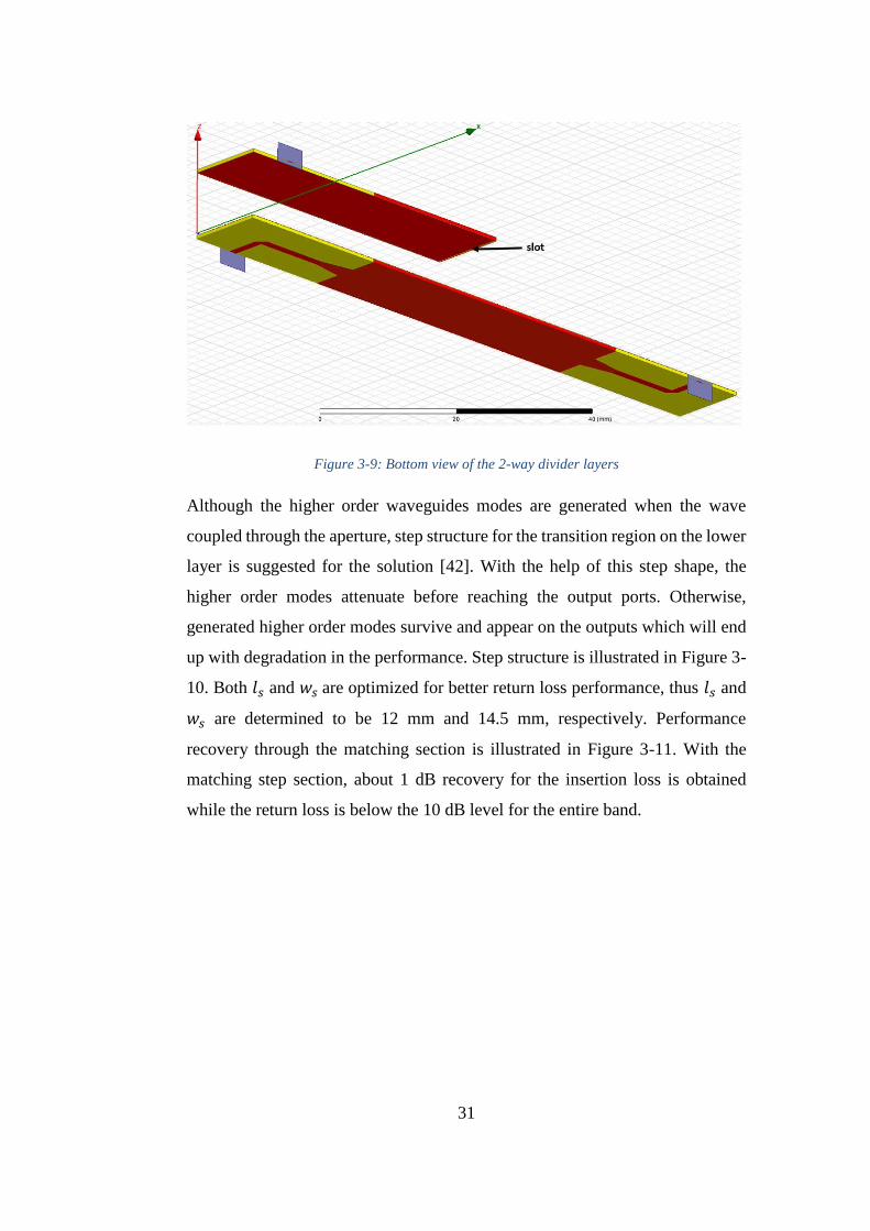
In order to verify the design parameters for the SIW section and the transition
parts, a thru line is formed by two back-to-back taper transition and a SIW
section in between, as shown in Figure 2-7. By considering 2-way and 4-way
divider designs, ports are located at the lateral edges and length of the line is
chosen accordingly. For this thru line, SIW section and microstrip part are both
5 cm in length and total length between the ports is 10 cm. Figure 2-8 presents
the E-field distribution of the SIW structure on HFSS simulation and the fact
that via arrays on SIW is able to guide the wave between the vias.

18
Figure 2-7: SIW thru line design
Figure 2-8: Field distribution of SIW thru line design
At the very beginning of the simulations, it is observed that the via arrays in the
SIW parts constitute a heavy burden to the simulation software due to the fact
that the number of the simulation meshes increase excessively, especially around
the vias. Although this cost is extremely high for the optimization process, there
is an equivalency between SIW and rectangular waveguide replacing all the vias

19
with metallic walls. In this study, the entire work is done with rectangular
waveguide and these models are replaced with the equivalent SIW models for
production. The rectangular waveguide model is illustrated in Figure 2-9. The
lateral walls are formed by using PEC sheets while the upper and lower walls
are made of copper. For radiation boundary, 5mm-heigth vacuum is placed on
the top of the structure. E-field distribution of the rectangular waveguide model
on HFSS simulation is illustrated in Figure 2-10.
Figure 2-9: Equivalent rectangular waveguide model for the SIW
20
Figure 2-10: Field distribution of rectangular waveguide model
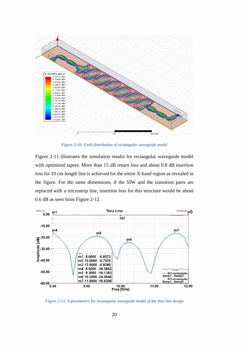
Figure 2-11 illustrates the simulation results for rectangular waveguide model
with optimized tapers. More than 15 dB return loss and about 0.8 dB insertion
loss for 10 cm-length line is achieved for the entire X-band region as revealed in
the figure. For the same dimensions, if the SIW and the transition parts are
replaced with a microstrip line, insertion loss for this structure would be about
0.6 dB as seen from Figure 2-12.
Figure 2-11: S-parameters for rectangular waveguide model of the thru line design
21
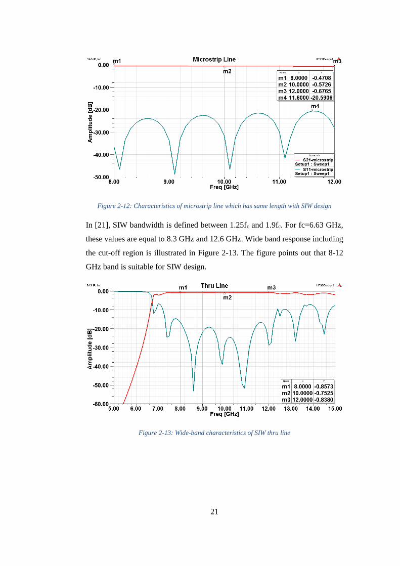
Figure 2-12: Characteristics of microstrip line which has same length with SIW design
In [21], SIW bandwidth is defined between 1.25fc and 1.9fc. For fc=6.63 GHz,
these values are equal to 8.3 GHz and 12.6 GHz. Wide band response including
the cut-off region is illustrated in Figure 2-13. The figure points out that 8-12
GHz band is suitable for SIW design.
Figure 2-13: Wide-band characteristics of SIW thru line

22
2.3. Equivalency between SIW and Rectangular Waveguide
In order to simplify the simulations for the SIW structure, the equivalent
rectangular waveguide model is used for all simulations, as mentioned before.
Now then, it is necessary to show this equivalency. In [24], theoretical derivation
for equivalency is made and using least square approach, equations (2-1) and (2-
2) are derived.
𝑓𝑐(𝑇𝐸10) =𝑐0
2∙√𝜖𝑟∙ (𝑎 −
𝑑2
0.95∙𝑠)−1 (2-1)
𝑓𝑐(𝑇𝐸20) =𝑐0
√𝜖𝑟∙ (𝑎 −
𝑑2
1.1∙𝑠−
𝑑3
6.6∙𝑠2)−1 (2-2)
These formulations indicates that the equivalent width, 𝑎𝑒 is slightly smaller than
the width between the centers of the vias and this drift as in (2-3) are determined
by the via diameters and the spacing between them.
𝑎𝑒 = 𝑎 −𝑑2
0.95𝑠 for 𝑠 < 𝜆0√𝜖𝑟/2 and 𝑠 < 4𝑑 (2-3)
Since the design parameters for this study are 𝑠 = 1 𝑚𝑚, 𝑑 = 0.5 𝑚𝑚, 𝜀𝑟 =
3.55 and 𝜆0 = 15.9 𝑚𝑚; the formulation is applicable. Using this formulation,
physical width 𝑎 is calculated as 12.26 mm. In order to superpose both the
equivalent waveguide and the physical SIW model, fine tuning for width 𝑎 is
applied on the calculated result. The tuned value for physical width is found as
12.2 mm and the results for both SIW and rectangular equivalent model are
plotted in Figure 2-14. It is seen from the figure that cut-off frequencies of the
models are very close to each other and the insertion loss characteristics are very
similar. These results support the equivalency between SIW and rectangular
waveguide and ensure the reliability of usage of metallic walls for lateral parts
instead of the via arrays for the simulations.

23
Figure 2-14: Comparison between SIW and rectangular waveguide models
2.4. TRL Calibration of SIW
Although, microstrip to SIW transition and thru line with coaxial ports designs
form significant parts of this study, microstrip and transition parts are not the
main concern. This study mainly investigates SIW architecture for power divider
design. Transmission media between SIW and measurement ports adversely
affect the design performance arising from the mismatches and losses. Thus, it
is appropriate to use thru-reflect-line (TRL) calibration technique in order to
extract non-coaxial parts from the design and to measure the design from
intrinsic SIW ports.
Likewise short-open-load-thru (SOLT) calibration, TRL calibration relocates the
reference planes of measurement. While SOLT calibration moves these
reference planes to the coaxial ports of DUT, TRL calibration shifts them to non-
coaxial intrinsic ports. Unlike SOLT, TRL calibration needs distinct calibration
standards and each should have a unique design. In Figure 2-15, TRL standards
for this study are given. Microstrip and transition parts of the thru line design are
kept the same for all calibration standards.

24
Figure 2-15: TRL Standards
With TRL calibration, reference planes for the measurement are placed 𝜆𝑔/4
inside from the SIW edges (Figure 2-16) while guided wavelength, λg is
calculated as 22.2 mm using [41]. Thus, the length of the thru standard is equals
to 𝜆𝑔/2 which is 11.1 mm. As reflect standard, either short or open standard can
be used. Due to radiation problem for open standard, shorted line is chosen as
reflect standard. Short calibration standard is designed by placing metallized vias
on the reference plane of the TRL calibration. Lastly, by enlarging the thru
standard with 𝜆𝑔/4 SIW line section, line standard is designed as 3𝜆𝑔/2. By
applying TRL calibration, mismatches and losses are eliminated and
performance of the SIW design is obtained. Moreover, microstrip to SIW
transitions are validated by comparing TRL and SOLT calibration results.
Figure 2-16: TRL reference planes for TRL calibration

25
CHAPTER 3
E-PLANE SIW POWER DIVIDER DESIGN
Since the intended divider design is in E-plane configuration, multilayer design
is necessary unlike single layer H-plane division. A 3-D E-plane power divider
design is demonstrated in Figure 3-1 which is obtained by placing a SIW stub
vertically on the aperture on another SIW line [32]. With this design,
practicability of E-plane division is shown while its 3-D structure limits the
usability of it. In this study, E-plane divider is designed in 2-D form by folding
the sum port on the division ports. To do this, two thin SIW layers are placed
one on the top of the other and coupled to each other via thin slots.
Figure 3-1: 3-D E-plane power divider design [32]

26
3.1. Layer-to-Layer Transition
Since the divider type is multilayered and power division occurs on transition,
design of this part carry importance. For equal power division, geometry of the
transition should be chosen carefully. Although T-shape of the structure leads to
impedance mismatch, this can be removed through some modifications applied
on this region.
For coupling between the adjacent SIW layers, thin slots are used. These slots
are placed perpendicular to the wave propagation direction for both SIW layers
as demonstrated in Figure 3-2. These slots have the same dimensions and should
be aligned for effective coupling. If multilayer production technology such as
low temperature co-fired ceramic (LTCC) was used, this alignment problem
would have been solved by opening single slot on metal layer between adjacent
dielectric layers.
Figure 3-2: Coupling slot between adjacent SIW layers
The structure of the E-plane SIW power divider resembles the modified version
of conventional E-plane rectangular waveguide tee. This can be imagined as
folding the sum port on the division ports. This modification provides 2-D
structure for the E-plane division. E-field distribution is held the same with the
E-plane tee structure as it is shown in Figure 3-3. As expected, fields on division

27
ports are out of phase due to E-plane division. Middle conductor in the figure is
actually formed by the lower conductor of the upper layer and the upper
conductor of the lower layer. By soldering or only just contacting the conductors
to each other, electrical continuity can be ensured.
Figure 3-3: Field distribution around transition region
In order to direct the wave to the coupling slot, upper layer should be terminated
with a short circuit by inserting metallized via array just as the SIW walls. By
placing vias in a distance from the slot, shorted stub is formed which helps for
matching. In this study, the termination is positioned exactly at the end of the
slot and thus shorted stub is not required for matching. PEC sheet is used for
simulations as it can be seen in Figure 3-4. By selecting the slot width similar to
the dielectric thickness, smooth transition of the waves is achieved like the
rectangular waveguide tee structure.

28
Figure 3-4: Coupling slot and termination sheet
Not only the placement of the slot but also dimensions of it, have a great
importance for effective coupling. Slot geometry should not cause significant
mismatch and should transmit the incoming wave to the lower layer effectively.
In order not to narrow the wave path, slot width 𝑤𝑠𝑙𝑜𝑡is selected as the same with
the SIW width. With the same way, slot length 𝑙𝑠𝑙𝑜𝑡 is designated the same with
the dielectric thickness. For the slot dimensions, parametric optimization is
applied and resultant slot dimensions 𝑤𝑠𝑙𝑜𝑡 and 𝑙𝑠𝑙𝑜𝑡 are determined to be 12 mm
and 0.4 mm, respectively.
The design of the coupling slot is verified by designing a multi-layer thru line as
in Figure 3-5. It is obtained by folding the thru line design. Performance
comparison between these two thru lines is shown in Figure 3-6. It is clearly seen
that insertion loss performances are almost the same. Return loss performance
degrades about 5 dB for folded line but it is still below the -15 dB level. From
the results, it can be said that slot design with determined dimensions has an
insignificant impact on the total performance.

29
Figure 3-5: Multi-layer thru line design
Figure 3-6: Comparison between the single-layer and multi-layer thru lines
3.2. Matching
Having completed the slot design, power divider structure becomes ready to be
formed. Optimum dimensions for the microstrip transition and vias on the SIW
determined in the previous chapter, are used in the power divider design without

30
any modification. The initial design for the 2-way power divider whose upper
and lower layers are formed by the thru line structure is illustrated in Figure 3-
7. Figure 3-8 and Figure 3-9 demonstrates the layers of the divider and the
coupling slots between them.
Figure 3-7: Initial design for the 2-way divider
Figure 3-8: Top view of the 2-way divider layers
31
Figure 3-9: Bottom view of the 2-way divider layers
Although the higher order waveguides modes are generated when the wave
coupled through the aperture, step structure for the transition region on the lower
layer is suggested for the solution [42]. With the help of this step shape, the
higher order modes attenuate before reaching the output ports. Otherwise,
generated higher order modes survive and appear on the outputs which will end
up with degradation in the performance. Step structure is illustrated in Figure 3-
10. Both 𝑙𝑠 and 𝑤𝑠 are optimized for better return loss performance, thus 𝑙𝑠 and
𝑤𝑠 are determined to be 12 mm and 14.5 mm, respectively. Performance
recovery through the matching section is illustrated in Figure 3-11. With the
matching step section, about 1 dB recovery for the insertion loss is obtained
while the return loss is below the 10 dB level for the entire band.

32
Figure 3-10: Stepped waveguide for transition region
Figure 3-11: Comparison between straight and stepped dividers
3.3. 2-way Divider Design
Completing the design of the coupling slot and the matching mechanism for the
division mismatches, 2-way power divider design is obtained. Figure 3-12 shows
the field distribution of the 2-way divider design.

33
Figure 3-12: Field distribution of the 2-way divider
Considering the loss performance of the introduced power divider, one should
take into account the losses arising from the dielectric and conductor since they
are unavoidable and already exist for the thru line design. Since the thru line and
the divider have the same length, loss performance of the divider can be
compared with the thru line loss. In Figure 3-13, it is demonstrated that the total
loss for 2-way divider is about 4 dB, while the ideal divider loss is calculated as
3.8 dB by considering the 0.8 dB loss for the thru line in previous chapter.
Degradation in the return loss performance with respect to the thru line indicates
the mismatch during the layer-to-layer transition.

34
Figure 3-13: 2-way SIW power divider characteristics
In order to match all the ports in a power divider, a resistive element should be
placed between the division ports. Since the divider design in this study is to be
used as waveguide tee for antenna feeding network, output matching is not
necessary. On the other hand, the input port is already matched with the
symmetric structure and the matching section.
Another criterion for a divider is the amplitude and the phase unbalance.
Considering the purpose of the divider design, amplitude and phase unbalance
should be kept as low as possible for a balanced feeding. Figure 3-14 which
illustrates amplitude and phase unbalances simultaneously also shows that the
amplitude unbalance is less than ±0.07 dB. Due to the E-plane power division,
180° phase difference is observed as expected. For the entire X-band, phase
unbalance is about ±0.5°.

35
Figure 3-14: Amplitude and phase unbalance of the 2-way divider
3.4. 4-way Divider Design
For the 4-way SIW divider design, one more dielectric layer with two coupling
slots is added to 2-way divider design. The same design for the coupling slots
and the matching section is also used for this extra layer. 3-layered 4-way divider
structure is illustrated in Figure 3-15 and Figure 3-16. For the bottom layer, two
coupling slots and matching sections are inserted for the secondary divisions
while the middle layer containing three coupling slots which mate the slots on
the other layers. In order to decrease the coupling between the output ports,
microstrip parts are shortened.

36
Figure 3-15: Top view of the 4-way divider layers

37
Figure 3-16: Bottom view of the 4-way divider layers
The length of the wave path in the 4-way divider whose field distribution is given
in Figure 3-17 is almost the same with the length in the thru line, except the slot
transitions in the divider. For the design of the matching and the slot sections,
the same dimensions with the 2-way divider are used for the 4-way divider. To
assure robustness, these dimensions are optimized for the new design and it is
seen that the matching and the slot dimensions in the 2-way divider are also
optimum for the 4-way divider design.
Figure 3-17: Field distribution of the 4-way divider

38
Since wave passes through one more coupling slot and dielectric layer at this
time, matching performance degradation for the 4-way divider is expected to be
larger than the degradation in the 2-way divider. The characteristics of the 4-way
divider are presented in Figure 3-18. Since the return loss degradation is at an
unacceptable level for the upper half of the initial band, 4-way divider design is
realized in 8-10 GHz band as given in the figure. Considering the antenna design
whose maximum bandwidth is 1.5 GHz, 2 GHz band is adequate for the
remaining parts of the design. Average loss for this design is around 7 dB. If the
thru line loss of 0.8 dB is taken into account, division loss for this 4-way divider
is calculated as 0.2 dB.
Figure 3-18: The 4-way SIW power divider characteristics
Amplitude and phase unbalance performance is important for the 4-way divider,
when the feed network design is considered. Any unbalance in the feed network
results with degradation in the array performance since the intended array is fed
uniformly. Unbalance characteristics of the 4-way divider in Figure 3-19 for 8-
10 GHz band reveals that the amplitude unbalance is less than 0.3 dB for 4 output
ports. As in the 2-way divider, ports of 4-way divider are also out of phase.
Considering this 180° phase difference between the output ports, the phase
unbalance is found less than 2.5°, as revealed in Figure 3-20.

39
Figure 3-19: Amplitude unbalance of the 4-way divider
Figure 3-20: Phase unbalance of the4-way divider


41
CHAPTER 4
ANTENNA ARRAY WITH SIW FEED NETWORK DESIGN
For the design of the antenna array and the integration with the feed network,
methodology is given step by step. Following the aperture coupled single patch
antenna design, 4-element array is formed with the proper array dimensions and
this array section is combined with the modified version of the 4-way divider.
4.1. Aperture Coupled Patch Antenna
Aperture coupling for patch antenna is one of the most common feed method
and is chosen for this study since the antennas with coupling apertures are easy
to integrate with SIW divider structures. With the integration, a very thin and a
compact structure that contains both the feed network and the antenna array is
obtained. In this part, single antenna with coupling aperture design is explained.
The initial step for the design is determination of the patch dimensions which
are found from the analytical equations [37]. The center frequency for the
antenna is determined by considering the divider characteristics. Since the 4-way
divider was designed at 8-10 GHz, center frequency is chosen as 9 GHz. For the
initial design, the same material (20 mil RO4003) with the SIW divider design
is used. For this material, width of the patch 𝑊𝑝is calculated as 11.05 mm by
using the relevant equations in [37]. Effective length of patch antennas are equal

42
to half wavelength for dominant TM010 mode. Due to the fringing effects, patch
extends about ∆𝐿 for each sides, thus physical length is calculated to be smaller.
By using derived formulations in [37], physical length of the patch 𝐿𝑝is found
as 8.7 mm. Single patch design with the calculated dimensions is illustrated in
Figure 4-1. These dimensions are optimized in order to fix the center frequency
of the patch at 9 GHz with a good return loss characteristics. Optimized
dimensions are 𝑊𝑝 = 11 𝑚𝑚 and 𝐿𝑝 = 8.09 𝑚𝑚.
Figure 4-1: Design of the microstrip patch antenna
Another design criterion for aperture coupled patch antennas is the aperture
dimensions. Since this feeding aperture is closely related with efficiency, the
dimensions should be arranged well. Aperture geometry determines the coupling
level, the antenna gain and the input reflection. For an efficient design, aperture
and patch dimensions are optimized together. For the calculated dimensions of
the patch, optimum aperture sizes are determined as 𝑙𝑠 = 2.7 𝑚𝑚 and 𝑤𝑠 =
0.3 𝑚𝑚 and illustrated in Figure 4-2. This optimized slot is oriented parallel to
the radiating edges of the patch by considering the radiation pattern of the patch.

43
Figure 4-2: Illustration of the coupling slot
For the dimensions mentioned above, single patch antenna is simulated by
feeding from the aperture with waveport and its return loss, gain and radiation
performance is evaluated. These characteristics are presented in Figure 4-3, 4-4
and 4-5. From the Figure 4-3, it is seen that the bandwidth of this antenna is 150
MHz which corresponds to 1.6% fractional bandwidth.
Figure 4-3: Return loss performance of the patch antenna

44
For the single patch antenna, boresight antenna gain which is shown in Figure
4-4 is found as 5.2 dB at 9 GHz. In Figure 4-5, radiation pattern of the designed
patch antenna is revealed. Half power beamwidths for the E-plane and the H-
plane patterns are measured as 94° and 88°, respectively. Back lobe level for this
design is found as 20 dB below the main lobe level.
Figure 4-4: Gain characteristic of the patch antenna
Figure 4-5: Radiation pattern of the patch antenna

45
Balanis recommends to use thick substrate with a lower dielectric constant for
wider bandwidth and better efficiency [37]. With the help of this method,
thickness of the dielectric is increased from 20 mil to 60 mil with the same
dielectric material. With this new material, all optimizations for the patch
dimensions are renewed. Optimized dimensions are given in Table 4-1. Having
increased the dielectric thickness, decrease in coupling level is observed as
expected and to increase it, slot dimensions are enlarged.
Table 4-1: Optimized patch dimensions for 60 mil RO4003 material
Parameter Description Value
h Substrate thickness 1.524 mm
𝑊𝑝 Patch width 11 mm
𝐿𝑝 Patch length 7.1 mm
𝑤𝑠 Slot width 1 mm
𝑙𝑠 Slot length 5 mm
For the new substrate, antenna performance is observed and the return loss, gain
and radiation pattern characteristics are illustrated in Figure 4-6, 4-7 and 4-8,
respectively. As revealed in Figure 4-6, bandwidth is extended to 580 MHz
which is about four times larger than the bandwidth of the thin-substrate design.
With this improvement, gain of the single patch antenna increases to 5.6 dB, E-
plane and H-plane beamwidths become 100° and 88°, respectively.

46
Figure 4-6: Return loss performance of the patch antenna
Figure 4-7: Gain characteristic of the patch antenna

47
Figure 4-8: Radiation pattern of the patch antenna
After observing the bandwidth extension with the increasing substrate thickness,
another method recommended in [37] is applied for further improvement for the
bandwidth. The method points out that lowering the permittivity of the substrate
also extends the bandwidth. This method is applied together with the previous
one to provide further improvement. For this purpose, Rogers RT/duroid 5880
material with 125 mil thickness and 2.2 dielectric constant is used. With this
material, dielectric thickness is increased about six times and dielectric constant
is lowered 40% with respect to the initial design. Dimensions for optimized
design are given in Table 4-2. For this relatively thick substrate, the slot length
is extended to 12 mm which is the maximum length for the designed SIW feed
network.

48
Table 4-2: Optimized patch dimensions for 125 mil RT5880 material
Parameter Description Value
h Substrate thickness 3.175 mm
𝑊𝑝 Patch width 13.2 mm
𝐿𝑝 Patch length 8 mm
𝑤𝑠 Slot width 1.5 mm
𝑙𝑠 Slot length 12 mm
For this new material, performance upgrade is illustrated in Figure 4-9, 4-10 and
4-11. As revealed in Figure 4-9, bandwidth is enlarged about ten times with
respect to the initial design and seen to be 1470 MHz. Antenna gain also
increases and passes 6 dB slightly for 9 GHz. For this design both the E-plane
and the H-plane beamwidths become 86°.
Figure 4-9: Return loss performance of the patch antenna

49
Figure 4-10: Gain characteristic of the patch antenna
Figure 4-11: Radiation pattern of the patch antenna
In the patch antenna design, 3 different dielectric material are used for the
simulations and comparisons show that the operational bandwidth of the patch
antenna increases with a thicker dielectric and lower permittivity.

50
4.2. Array Design with SIW Feed Network
In this part, rectangular patch antenna array design is introduced by using the
single patch design. Since the designed SIW power divider is used as a feed
network, array design should be adaptable to SIW structure. Thus, feeding
apertures are designed accordingly. In order to use 4-way SIW power divider as
feed network, 4-element array is designed as illustrated in Figure 4-12 and 4-13.
For the initial array design, single patch design on 20 mil RO4003 material is
used. With this selection, structure consists of 4 layer 20 mil RO4003 material
and its total thickness equals 2.3 mm. The network is fed from the input port on
the top layer and transmitted to SIW region. Each layer has coupling slots to
conduct the wave to the next layer and in the end, wave radiates from the patch
antennas on the bottom layer.

51
Figure 4-12: Top view of the feed network and array design

52
Figure 4-13: Bottom view of the feed network and array design
Element spacing is another important parameter for array characteristics. In [43],
it is stated that performance degradation occurs for closely spaced array elements
due to high mutual coupling level. It is also stated that the element spacing
affects the main lobe beamwidth and side lobe level and half-wavelength spacing
is suggested to be the optimum distance. Following this, element spacing is
parametrically swept around the half-wavelength for this design to obtain the
desired performance. For 23 mm element spacing which is the optimum value
for the array design, the matching performance is shown in Figure 4-14. With
this 4-element array design, about 100 MHz frequency band is obtained.

53
Figure 4-14: Return loss performance of the patch antenna array
Since the array consists of 4 elements, antenna gain is expected to increase about
6 dB. From Figure 4-15, array gain measured as 10.5 dB. Figure 4-16 presents
the radiation pattern of the array design. Since 4x1 element array is designed,
radiation pattern in the array extension plane becomes narrower. For this design,
E-plane and H-plane beamwidths are 20° and 90°, respectively and the side lobe
level is obtained as 13 dB while the back-radiation level is 22 dB, as revealed in
Figure 4-16.
Figure 4-15: Gain characteristic of the patch antenna array

54
Figure 4-16: Radiation pattern of the patch antenna array
In the previous part, valid improvements for the performance of the single
antenna elements was obtained with thicker substrate and lower permittivity.
This recovery is applied also for the array design. For antenna substrate, 60 mil
Rogers 4003 material is used. With this relatively thick substrate, total thickness
for the structure becomes 3 mm. Bandwidth extension for the return loss can be
observed from Figure 4-17. With this material, 450 MHz frequency band is
achieved.

55
Figure 4-17: Return loss performance of the patch antenna array
Gain and radiation pattern characteristics of the design are given in Figure 4-18
and 4-19, respectively. With this new design, the antenna gain is increased to 11
dB while the main lobe beamwidths and side lobe levels remain the same with
thin substrate as it can be seen from Figure 4-19.
Figure 4-18: Gain characteristic of the patch antenna array

56
Figure 4-19: Radiation pattern of the patch antenna array
In order to increase the bandwidth of the array design further as in the single
element, Rogers RT/duroid 5880 material with 125 mil thickness and 2.2
dielectric constant is applied for the array design. For this design, desired return
loss response is not obtained as revealed in Figure 4-20. Low coupling level
arising from the thick antenna layer and the mismatch due to the permittivity
difference between the substrates might be the possible explanations for this
unacceptable response. Despite this degraded return loss performance, obtained
structure radiates similar with the previous design. Gain and radiation patterns
of this antenna array are presented in Figure 4-21 and 4-22, respectively.

57
Figure 4-20: Return loss performance of the patch antenna array
Figure 4-21: Gain characteristic of the patch antenna array

58
Figure 4-22: Radiation pattern of the patch antenna array
Among these array designs with three different materials, the design with 60 mil
RO4003 material provides satisfactory results in terms of radiation pattern and
matching performance. For this design, some modifications are applied in order
to decrease the back radiation level of the arrays. For this purpose, the antenna
layer is extended in H-plane direction. With this extension, metal coverage on
the antenna layer behaves like a large ground plane and it minimizes the back
radiation level. The radiation pattern of the design with enlarged ground plane is
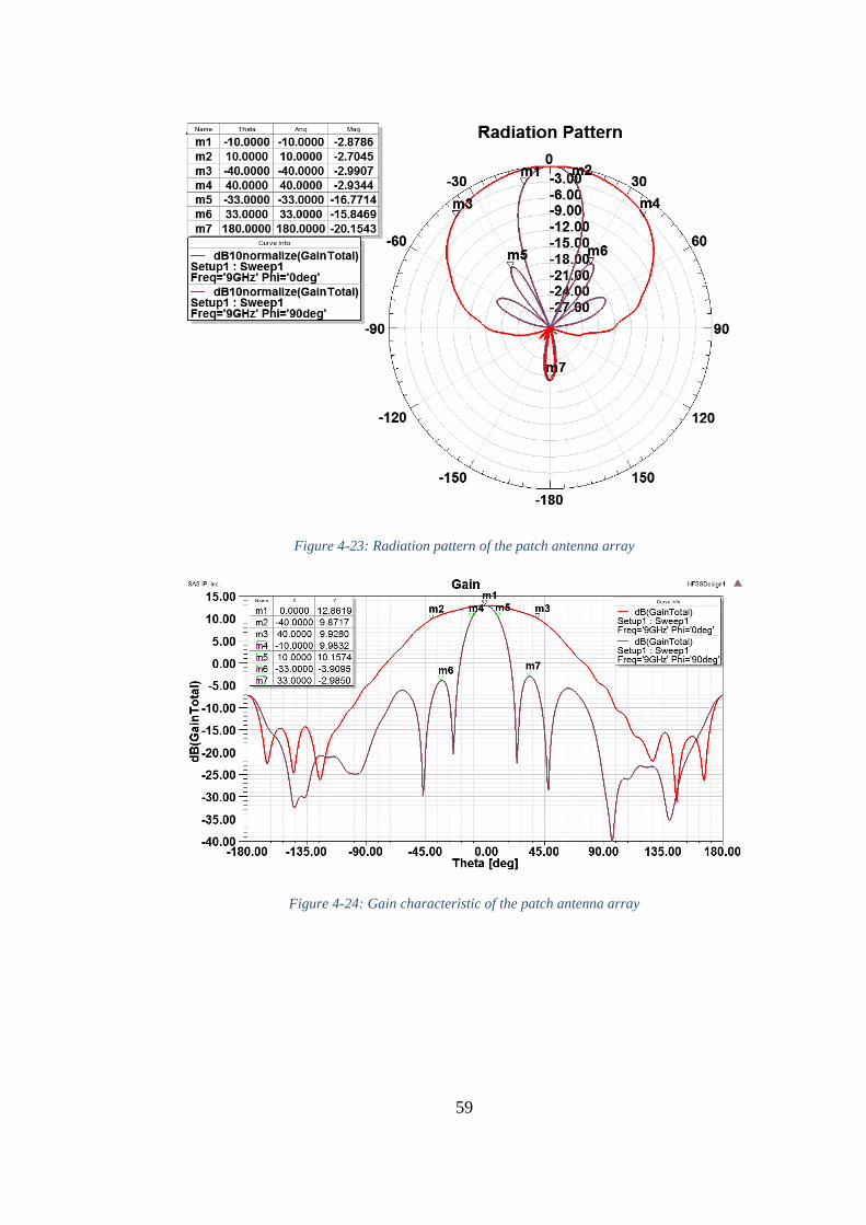
illustrated in Figure 4-23. Lowering back radiation level made the antenna array
more directive. This modification reduces the H-plane beamwidth from 90° to
80° as can be seen from the radiation plot. With lowered back radiation, increase
in the main lobe gain is inevitable. Recovered gain performance is given in
Figure 4-24. As obtained from the plot, main lobe gain reaches 12.8 dB which is
almost 2 dB more than the previous design with narrow ground plane.
59
Figure 4-23: Radiation pattern of the patch antenna array
Figure 4-24: Gain characteristic of the patch antenna array


61
CHAPTER 5
FABRICATION OF THE DESIGNS AND MEASUREMENT
RESULTS
Design steps for the SIW feed microstrip patch antenna array are introduced step
by step so far. Desired structure is composed with the help of the simulation
results. In order to verify the designs are produced and relevant performance
parameters are measured. Each step is separately manufactured and the
measurement results are compared with the simulation results.
5.1. Fabrication of the Thru Line and Calibration Standards
While the design steps proceed, initial fabrication for the study is implemented
with the thru line production. Fabrication of the thru line has a great importance
for the futurity of the study. It is no wonder that a successful thru line fabrication
facilitates the remaining production work. Therefore, importance is given for the
thru line and some modifications for the production are applied for the best
results.
At the very beginning of the fabrication, the smallest possible via diameter 0.3
mm is used for the SIW part, however, there observed some unplated via holes
after the metalizing process. This is mainly because of the fact that metallizing
material could not penetrate some of these narrow via holes. With these unplated

62
vias, incoming wave could not be guided. Thereon, via diameter is extended to
0.5 mm as specified in the second chapter. For this diameter, the same problem
has not been observed anymore. Initial fabrication of the thru line is shown in
Figure 5-1 for which, solderable end launch SMA connectors are used.
Figure 5-1: Initial thru line design with solderable end launch connectors
Introduced thru line design is measured and a mismatch issue arising from the
SMA connectors is detected. In order to minimize this mismatch, matching
capacitive stubs placed near the connectors since they have an inductive effect.
Initially, copper strip pieces are pasted as capacitive stubs. Having found the
optimum stub dimensions, these pieces are added to the design and the thru line
with these stubs are manufactured. Matching stubs can be seen in Figure 5-1.
With these stubs, return loss performance is improved and pulled below 10 dB
for almost whole X-band as illustrated in Figure 5-2.
capacitive
stubs

63
Figure 5-2: Thru line design with 3 different configurations
Despite this improvement in the matching performance, connector in use is
replaced by Southwest Microwave’s “292-05A-5” end launch connector. For
this connector, no soldering is required and the connection is provided by
compressing screws. This connector is chosen because of its low VSWR
performance. Measurement result of the design with these connectors is also
drawn in Figure 5-2. As it can be seen from the figure, there is no need to use
stubs for matching purpose with this connector. Final structure for the thru line
design is shown in Figure 5-3. For this thru line, simulation and measurement
results are drawn in Figure 5-4 and 5-5. From the measurement results, average
insertion loss is obtained as 1.65 dB for the entire X-band while this value was
0.8 dB for the simulation result. Since the connectors did not appear in the
simulations, difference in the simulation and the measurement results was
expected.
Figure 5-3: Thru line design

64
Figure 5-4: Insertion loss performance of the thru lines
Figure 5-5: Return loss performance of the thru lines
On the purpose of insertion loss recovery, another modification is tried. The vias
in the SIW structure are replaced with thin slots as revealed in Figure 5-6. With
the help of these metallized slots, it is aimed to reduce the leakage loss if there
was effectively any. Considering the rigidity of the structure, small notches are
placed in these slots. Comparison between the thru lines with vias and slots is

65
also presented in Figure 5-4 and 5-5. For this thru line with slots, average
insertion loss is measured as 1.7 dB which is similar to the via design. This
similarity reveals that the leakage loss due to the via array design is negligible
since the insertion losses are almost same with continuous and discrete wall
designs. By this way, via dimensions and separation between them has been
validated. On the other hand, this slot design for lateral walls can still be useful
in terms of fabrication easiness and drilling time consumption by taking the
similar characteristics of both structures into consideration.
Figure 5-6: Thru line design with slots
As mentioned in the second chapter, TRL calibration is used for all of the
fabricated designs. Calibration standards are fabricated as indicated for both thru
lines with vias and slots. These standards are shown in Figure 5-7. Microstrip
parts and connectors for the calibration standards are the same with the thru line
design and with the help of these standards, measurement planes are relocated
on the SIW portion. In Figure 5-8, measurement setup with the calibration
standards and calibrated network analyzer is given. After the TRL calibration,
thru standard is measured and a return loss above 40 dB is obtained.

66
Figure 5-7: TRL calibration standards for both via and slot designs
Figure 5-8: Calibration standards and measurement setup
Characteristics of the thru line designs with TRL calibration are plotted in Figure
5-9. Calibration process removes the portion of the insertion loss whose source
is coaxial connectors and microstrip parts. With the help of the TRL calibration,
pure SIW structure which is 5 cm in length, is measured without the microstrip

67
parts and connectors. As a result, average SIW thru line loss is measured to be
0.53 dB while the return loss is above 15 dB for the entire band.
Figure 5-9: Thru line characteristics with TRL calibration
5.2. Fabrication of the 2-Way and 4-Way Dividers
For the divider implementation, the most important step is the integration of the
divider layers. In this part, applied methods for this integration and measurement
results is introduced. Fabricated layers are shown in Figure 5-10 and Figure 5-
11, before the integration process. As the figures reveal, coupling slots on both
layers have exactly the same dimensions and they should be strictly overlapped
for a good matching and coupling performance. Many screw holes are placed in
order to ensure this alignment as well as the rigidity of the structure.

68
Figure 5-10: Outer surfaces of the 2-way divider layers
Figure 5-11: Inner surfaces of the 2-way divider layers
By unifying the layers with the help of the conductive screws, electrical
continuity between the layers is already provided. Moreover, tightly screwing
the layers increases the contact between the ground planes of the layers
effectively and decreases the contact resistance. Nevertheless, as a trial, the
layers are soldered in order to support the electrical continuity between the
layers. For the soldering process, gel solder is applied to contact the surfaces as
revealed in Figure 5-12. Thin heat proof strips are used in order to prevent the
solder to leak the coupling slots. Then, prepared layers are screwed and heated
in a reflow oven. Measurement results of the soldered and the solderless dividers
are compared in Figure 5-13. It is clearly seen that both the insertion loss and the

69
return loss performances are not effected significantly with soldering. These
results indicate that the mounting screws and physical contact are adequate for
the electrical continuity and the use of solder for an improved contact is not
necessary. For the remaining manufacturing processes, only mounting screws
are used.
Figure 5-12: 2-way divider layers with gel solder and insulator strip
Figure 5-13: Comparison between soldered and solderless dividers
The final design of the 2-way divider after the mounting is shown in Figure 5-
14 and 5-15. With the help of the screws and end launch connectors, quite rigid
2-layered divider is obtained. Measurement results with this fabricated divider

70
are given in Figure 5-16 and 5-17. About 5 dB insertion loss is observed while
it is about 4dB for the simulation results for 8-10 GHz region. Oscillating
characteristics of the insertion loss plot indicates that the mismatches arising
from the connectors and microstrip to SIW transitions degrade the divider
performance. It is expected that these mismatches would be removed with the
help of the TRL calibration. Calibration process and calibrated results are also
given in this part. On the other hand, measured return loss values are quite alike
with the simulation result.
Figure 5-14: Top view of the 2-way divider
Figure 5-15: Bottom view of the 2-way divider

71
Figure 5-16: Insertion loss performance of the 2-way dividers
Figure 5-17: Return loss performance of the 2-way dividers
TRL calibration is held for the 2-way divider as well, in order to observe SIW
power divider characteristics without the effects of the connectors and microstrip
parts. Since these parts are same with thru line design, previous TRL calibration
was used for 2-way divider measurements. Results are presented in Figure 5-18
for both the insertion and the return losses. As it can be seen from the figure,
performance of the divider degrades towards the end of the measurement band.
Despite this degradation, desired 2-way divider is obtained for 8-11 GHz
frequency band. Through this region, average insertion loss is 3.75 dB. Taking

72
the fact that the SIW thru line has 0.5 dB insertion loss into consideration, it can
be stated that a quite efficient division is obtained with the E-plane SIW divider.
Figure 5-18: Measurement results of the 2-way divider with TRL calibration
Amplitude and phase unbalances are another important parameters for the
divider performance. Since this divider is intended to be used in antenna feed
network, special interest is undertaken for the divider fabrication by keeping the
symmetry and equating the line lengths. Measured unbalance values are plotted
in Figure 5-19 with the simulation results. Since the simulation results do not
reflect the production deficiencies and tolerances as well as the connector
mounting effects, unbalance values for the simulation results are very low with
respect to measurement results. Nevertheless, measured unbalance values are
still at acceptable level for a 2-way divider design. The amplitude unbalance is
less than ±0.6 dB and the phase unbalance values are 8° at most by taking into
account 180° phase difference between E-plane divider ports. TRL calibration
imperfectness and connector mounting deficiencies are expected to be sources
of this 4° shift for the phase unbalance values.

73
Figure 5-19: Amplitude and phase unbalance of the 2-way divider
For the 4-way divider, same fabrication and mounting methods are applied.
Since the 4-way divider contains 3 coupling slots, mounting screws are placed
accordingly. Also, division arms are shortened in order to decrease the coupling
between the neighbour arms. 4-way divider layers are presented in Figure 5-20
and 5-21, before mounting.
Figure 5-20: Outer surfaces and middle layer of the 4- way divider
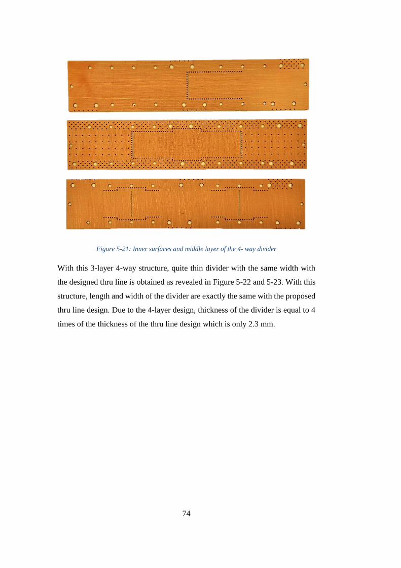
74
Figure 5-21: Inner surfaces and middle layer of the 4- way divider
With this 3-layer 4-way structure, quite thin divider with the same width with
the designed thru line is obtained as revealed in Figure 5-22 and 5-23. With this
structure, length and width of the divider are exactly the same with the proposed
thru line design. Due to the 4-layer design, thickness of the divider is equal to 4
times of the thickness of the thru line design which is only 2.3 mm.

75
Figure 5-22: Top view of the 4-way divider
Figure 5-23: Bottom view of the 4-way divider
Measurement results are plotted in Figure 5-24 and 5-25 with the simulation
results. Mismatch oscillations and insertion loss degradations are caused by the
connector mounting and microstrip to SIW transition part as in the 2-way divider
design. By applying TRL calibration, these effects are removed and pure SIW
characteristics are obtained.

76
Figure 5-24: Insertion loss characteristics of the 4-way divider
Figure 5-25: Return loss characteristics of the 4-way divider
Since the division arms of the 4-way divider is different from the thru line design,
calibration standards for 4-way divider are separately designed. Measurement
results after TRL calibration are plotted in Figure 5-26 and 5-27. As marked in
the return loss plot, input matching is obtained in 9.3- 10.5 GHz band for the
fabricated design. After TRL calibration, average insertion loss of the 4-way
SIW divider for this frequency band is found to be 6.85 dB. Considering the fact
that the thru line has 0.53 dB insertion loss with TRL calibration, it can be said
that the proposed divider design is very effective in terms of loss performance.

77
Figure 5-26: Insertion loss characteristics of the 4-way divider with TRL calibration
Within the obtained frequency band, amplitude and phase unbalances are
calculated for the fabricated 4-way divider. In Figure 5-27, measured unbalance
values are presented with the simulation results. From the fabricated design,
below 1 dB amplitude unbalance and below 8° phase unbalance are obtained for
the entire band. For these unbalance values, it is evaluated that whether they are
tolerable or not with the help of the measurement results of the array design.
Figure 5-27: Amplitude and phase unbalance of the 4-way divider

78
5.3. Fabrication of the Patch Antenna Array with SIW Feed
Network
Fabrication process ends up with the antenna array production. Figure 5-28 and
5-29 illustrate the antenna and feed network layers. All layers have the same
dimensions in length and width. For entire structure, RO4003 material is used
and thicknesses are 20 mil for feed layers and 60 mil for antenna layer. With this
layers, antenna system is constructed as it can be seen in Figure 5-30 and 5-31.
Figure 5-28: Top view of the antenna array and feeding structure layers

79
Figure 5-29: Bottom view of the antenna array and feeding structure layers
Figure 5-30: Top view of the antenna array network

80
Figure 5-31: Bottom view of the antenna array network
Initial measurement is held for the return loss characteristics of the fabricated
design and results are plotted in Figure 5-32. Input matching is obtained for 200
MHz band with fabricated design while it is 450 MHz for the simulation. Due to
the fabrication tolerances, center frequency of the antenna array is shifted to the
right.
Figure 5-32: Return Loss measurement of the Antenna Array
For the radiation characteristics of the product, Satimo’s Starlab spherical near
field antenna measurement system [44] is used as shown in Figure 5-33. The far
field characteristics is obtained with the system which measures the near field

81
characteristics and then evaluate them for the far field response. Placement of
the antenna and the measurement probes can be seen in Figure 5-34.
Figure 5-33: Satimo'sStarlab product [44]

82
Figure 5-34: The antenna placement and the measurement probes of the near field
measurement system
Boresight gain of the array is measured for 8.5-9.5 frequency band. As plotted
in Figure 5-35, array gain is above 10 dB between 9.1-9.3 GHz. With this gain
performance antenna radiates effectively for 200 MHz band.

83
Figure 5-35: Characteristics of the array gain for 8-10 GHz band
The antenna gain is maximum at 9.2 GHz with 10.52 dB gain while the
simulation results shows 11.10 dB gain for the same design. The simulation and
the measurement results for the radiation pattern is plotted together in Figure 5-
36. E-plane and H-plane beamwidths are measured 18° and 70°, respectively.
Side lobe and back lobe levels are measured as 11 dB and 21 dB, respectively.
Figure 5-36: Radiation patterns for the simulation and the measurement


85
CHAPTER 6
CONCLUSIONS AND FUTURE STUDIES
This study describes the antenna array and the feed network design based on the
SIW power divider. Starting with the formation of the SIW transmission line by
making use of the basic design criteria in the literature, a valid waveguide is
constructed in planar form. Acquired SIW is transformed to a transmission line
with microstrip measurement ports by integrating it with the microstrip-to-taper
transitions. At the end of the process, a hybrid line including both SIW and
microstrip transmission media is obtained. The simulations reached 0.8 dB
insertion loss for this 10-cm hybrid line while this value is around 1.7 dB for
measurements due to the connectors that are not modelled. Fortunately, effects
of the connectors and microstrip parts are extracted from the measurement with
TRL calibration and pure SIW insertion loss performance for 5-cm line is
obtained as 0.5 dB for the entire X-band region.
E-plane SIW power divider is derived from the basis of the SIW thru line design.
Through the coupling slot between the layers, 2-layered E-plane SIW power
divider is achieved for 8-11 GHz frequency band. For this 3 GHz band, total
divider loss in the SIW media is about 3.75 dB while the thru line of the same
length with this divider has 0.5 dB loss. The same design steps are applied for 4-
way power divider design with 3-layered structure. A matched divider is
achieved in 9.3-10.5 GHz band with 6.85 dB insertion loss.

86
For the usage of the SIW divider in the antenna feed network, the output layer
of the 4-way divider design is modified and the microstrip output ports are
replaced with the radiation slots. With this step, the feed network design has been
completed and 4-elements antenna array layer is mounted upon it. At the end,
compact antenna array and feed network is obtained by keeping their lengths and
widths the same by joining the layers one under the other. Antenna measurement
results validate the design with the results of 10.5 dB boresight gain.
The study contributes to the relevant literature by revealing the feasibility of an
E-plane SIW feed network for a microstrip antenna array. Through the study,
SIW thru line, 2-way and 4-way power divider designs supplement the main
propose with the help of the previous studies. With this design, various SIW
components have been designed and produced while the step-by-step
representation of the design has simplified the process.
Future study in this particular subject may bring about further improvements
some of which are given. Feeding larger number of antenna elements in array
through SIW network by increasing the number of the division might be a future
study. With n-layered structure, 2n-1 division factor can be obtained as long as
the input matching is provided. Regardless of the division number, structure
would have exactly the same dimensions in length and width with the array
dimensions while only the depth increases with the increasing number of layers.
Another contribution might be an unequal SIW power divider design. By this
means, non-uniform feeding for antenna array can be obtained with SIW
network.

87
REFERENCES
[1] K. Wu, D. Deslandes and Y. Cassivi, "The Substrate Integrated Circuits -
A New Concept for High-Frequency Electronics and Optoelectronics," in
6th International Conference on Telecommunications in Modern Satellite,
Cable and Broadcasting Service (TELSIKS), Serbia and Montenegro, Nis,
October 1-3, 2003.
[2] F. Shigeki, "Waveguide line". Japan Patent 06-053 711, 25 Feb. 1994.
[3] M. Bozzi, F. Xu, D. Deslandes and K. Wu, "Modelling and Design
Considerations for Substrate Integrated Waveguide Circuits and
Components," in 8th International Conference on Telecommunications in
Modern Satellite, Cable and Broadcasting Services (TELSIKS), Serbia,
Nis, September 26-28, 2007.
[4] D. Deslandes and K. Wu, "Single-Substrate Integration Technique of
Planar Circuits and Waveguide Filters," IEEE Transactions on Microwave
Theory and Techniques, vol. 51, no. 2, pp. 593-596, February 2003.
[5] Y. Cassivi, D. Deslandes and K. Wu, "Substrate Integrated Waveguide
Directional Couplers," in 2002 Asia-Pacific Microwave Conf. Proc.,
Kyoto, Japan, 2002.
[6] S. Germain, D. Deslandes and K. Wu, "Development of Substrate
Integrated Waveguide Power Dividers," in CCECE 2003 - CCGEI 2003,
Montreal, 4-7 May 2003.
[7] W. D'Orazio and K. Wu, "Substrate-Integrated-Waveguide Circulators
Suitable for Milimeter-Wave Integration," IEEE Transactions on
Microwave Theory and Techniques, vol. 54, no. 10, pp. 3675-3680, 2006.
[8] S. Adhikari, A. Ghiotto, S. Hemour and K. Wu, "Tunable Non-Reciprocal
Ferrite Loaded SIW Phase Shifter," in IEEE MTT-S International
Microwave Symposium Digest (IMS), 2-7 June 2013.
[9] F. F. He, K. Wu, W. Hong, L. Han and X. Chen, "A Low Phase-Noise
VCO Using an Electronically Tunable Substrate Integrated Waveguide
Resonator," IEEE Transactions on Microwave Theory and Techniques ,
vol. 58, no. 12, pp. 3452-2458, 2010.
[10] Y. Cassivi and K. Wu, "Low Cost Microwave Oscillator Using Substrate
Integrated Waveguide Cavity," IEEE Microwave and Wireless
Components Letters, vol. 13, no. 2, pp. 48-50, 2003.

88
[11] J. Xu and K. Wu, "A Subharmonic Self-Oscillating Mixer Using Substrate
Integrated Waveguide Cavity for Milimeter-Wave Application," in IEEE
MTT-S International Microwave Symposium Digest, California, 2005.
[12] K. Niotaki, F. Guippi, A. Collado and A. Georgiadis, "A Broadband Power
Amplifier Based on Composite Right/Left-Handed Half-Mode Substrate
Integrated Waveguide," in Proc. DCIS 2013, San Sebastian, 2013.
[13] T. Erdöl, "X-band RF Switch Implementation in Substrate Integrated
Waveguide," Ph.D Thesis, 2012.
[14] K. Wu, "Substrate Integrated Waveguides," Short Course in 43rd European
Microwave Conference (EuMC), Nuremberg, 2013.
[15] F. Xu and K. Wu, "Guided-Wave and Leakage Characteristics of Substrate
Integrated Waveguide," IEEE Transactions on Microwave Theory and
Techniques, vol. 53, no. 1, pp. 66-73, 2005.
[16] L. Yan, W. Hong, K. Wu and T. Cui, "Investigations on the propagation
characteristics of the substrate integrated waveguide based on the method
of lines," Microwaves, Antennas and Propagation, IEEE Proceedings, vol.
152, no. 1, pp. 35-42, 2005.
[17] D. Deslandes and K. Wu, "Accurate Modelling, Wave Mecanisms, and
Design Considerations of a Substrate Integrated Waveguide," IEEE
Transactions on Microwave Theory and Techniques, vol. 54, no. 6, pp.
2516-2526, 2006.
[18] L. Li, X.-P. Chen, K. Roni and K. Wu, "A Transition from Substrate
Integrated Waveguide (SIW) to Rectangular Waveguide," in Asia Pacific
Microwave Conference, APMC 2009, Singapore, 2009.
[19] A. Morini, M. Farina, C. Cellini, T. Rozzi and G. Venanzoni, "Design of
Low-Cost Non-Radiative SMA-SIW Launchers," in 36th European
Microwave Conference, Manchester, 2006.
[20] D. Deslandes and K. Wu, "Integrated Microstrip and Rectangular
Waveguide in Planar Form," IEEE Microwave and Wireless Components
Letters, vol. 11, no. 2, pp. 68-70, 2001.
[21] D. Deslandes, "Design Equations for Tapered Microstrip-to-Substrate
Integrated Waveguide Transitions," in IEEE MTT-S International
Microwave Symposium Digest (MTT), California, 2010.
[22] K. Lu, "An Efficient Method for Analysis of Arbitrary Nonuniform
Transmission Lines," IEEE Transactions on Microwave Theory and
Techniques, vol. 45, no. 1, pp. 9-14, 1997.

89
[23] D. Deslandes and K. Wu, "Integrated Transition of Coplanar to
Rectangular Waveguides," in IEEE MTT-S International Microwave
Symposium Digest, Arizona, 2001.
[24] Y. Cassivi, L. Perregrini, P. Arcioni, M. Bressan, K. Wu and G. Conciauro,
"Dispersion Characteristics of Substrate Integrated Rectangular
Waveguide," IEEE Microwave and Wireless Components Letters, vol. 12,
no. 9, pp. 333-335, 2002.
[25] E. Diaz Caballero, A. Belenguer, H. Esteban and V. Boria, "Thru-reflect-
line Calibration for Substrate Integrated Waveguide Devices with Tapered
Microstrip Transitions," Electronics Letters, vol. 49, no. 2, pp. 132-133,
2013.
[26] Z.-Y. Zhang and K. Wu, "Broadband Half-Mode Substrate Integrated
Waveguide (HMSIW) Wilkinson Power Divider," in IEEE MTT-S
International Microwave Symposium Digest, Atlanta, 2008.
[27] D. Eom, J. Byun and H.-Y. Lee, "Multi-Layer Four-Way Out-of-Phase
Power Divider for Substrate Integrated Waveguide Applications," in IEEE
MTT-S International Microwave Symposium Digest, Boston, 2009.
[28] P. Mohammadi and Ş. Demir, "Two Layers Substrate Integrated
Waveguide Power Divider," in XXXth URSI General Assembly and
Scientific Symposium, İstanbul, 2011.
[29] P. Mohammadi, "Low loss substrate integrated waveguide n-way power
divider," PhD. Thesis, 2012.
[30] F. F. He, K. Wu, W. Hong, H.-J. Tang, H.-B. Zhu and J. X. Chen, "A planar
Magic-T Using Substrate Integrated Circuits Concept," IEEE Microwave
and Wireless Components Letters, vol. 18, no. 6, pp. 386-388, 2008.
[31] K. Song, Y. Fan, G. Yue and B. Zhang, "Novel Substrate Integrated
Waveguide Layer-to-layer Transitions," in Asia-Pacific Microwave
Conference, APMC 2008, Hong Kong, 2008.
[32] B. Y. El Khatib, T. Djerafi and K. Wu, "Substrate-Integrated Waveguide
Vertical Interconnects for 3-D Integrated Circuits," IEEE Transactions on
Components, Packaging and Manufacturing Technology, vol. 2, no. 9, pp.
1526-1535, 2012.
[33] Z. Zhang, K. Wu and N. Yang, "Broadband Millimeter-Wave Quasi-Yagi
Antenna Using Substrate Integrated Waveguide Technique," in IEEE
Radio and Wireless Symposium, Orlando, 2008.
[34] K. Kim, J. Byun and H.-Y. Lee, "Substrate Integrated Waveguide Quasi
Yagi Antenna Using SIW-to-CPS Transition for Low Mutual Coupling,"

90
in IEEE Antennas and Propagation Society International Symposium
(APSURSI), Toronto, 2010.
[35] A. Bakhtafrooz and A. Borji, "Novel Two-Layer Milimeter-Wave Slot
Array Antennas Based on Substrate Integrated Waveguides," Progress in
Electromagnetics Research, vol. 109, pp. 475-491, 2010.
[36] D. M. Pozar, "A Review of Aperture Coupled Microstrip Antennas:
History, Operation, Development and Applications," A review of Aperture
Coupled Microstrip Antennas: History, Operation, Development, and
Applications, 1996.
[37] C. A. Balanis, Antenna Theory - Analysis and Design, New Jersey: John
Wiley & Sons, Inc., 2005.
[38] W. M. Abdel-Wahab and S. Safavi-Naeini, "Wide-Bandwidth 60-GHz
Aperture-Coupled Microstrip Patch Antennas (MPAs) Fed by Substrate
Integrated Waveguide (SIW)," IEEE Antennas and Wireless Propagation
Letters, vol. 10, pp. 1003-1005, 2011.
[39] T. Mikulasek, A. Georgiadis, A. Collado and J. Lacik, "2x2 Microstrip
Patch Antenna Array Fed by Substrate Integrated Waveguide for Radar
Applications," IEEE Antennas and Wireless Propagation Letters, vol. 12,
pp. 1287-1290, 2013.
[40] "ANSYS HFSS v.15.0.2," SAS IP, Inc., 2013.
[41] D. M. Pozar, Microwave Engineering, vol. b, Toronto: John Wiley & Sons,
1998, p. b.
[42] Q. Zhang and Y. Lu, "E-band "T" Shape Transitions between Substrate
Intagrated Waveguide and Standard Waveguide," in Asia-Pacific
Microwave Conference , Hong Kong, 2008.
[43] S. Choudhari, K. P. Ray and S. Kulkarni, "Design and Development of 4
Element Linear Microstrip Patch Antenna Array with Null Steering by
Phase Control," in International Conference on Sustainable Energy and
Intelligent Systems (SEISCON 2011), Chennai, India, 2011.
[44] "Starlab Antenna Measurement Systems," Satimo, [Online]. Available:
http://www.satimo.com/content/products/starlab. [Accessed 6 July 2014].