Design and Manufacturing Method of Fundamental Beam Mode ...
13
materials Article Design and Manufacturing Method of Fundamental Beam Mode Shaper for Adapted Laser Beam Profile in Laser Material Processing Christian Bischoff 1,2, *, Friedemann Völklein 3 , Jana Schmitt 3 , Ulrich Rädel 1 , Udo Umhofer 1 , Erwin Jäger 1 and Andrés Fabián Lasagni 2,4 1 Topag Lasertechnik GmbH, Nieder-Ramstädter-Str. 247, 64285 Darmstadt, Germany 2 Institut für Fertigungstechnik, Technische Universität Dresden, George-Bähr-Str. 3c, 01069 Dresden, Germany 3 Institut für Mikrotechnologien, Hochschule RheinMain, Am Brückweg 26, 65428 Rüsselsheim, Germany 4 Fraunhofer-Institut für Werkstoff-und Strahltechnik IWS, Winterbergstr. 28, 01277 Dresden, Germany * Correspondence: bischoff@topag.de; Tel.: +49-6151-425978 Received: 13 June 2019; Accepted: 9 July 2019; Published: 13 July 2019 Abstract: Many laser material processing applications require an optimized beam profile, e.g., ring shape or Top-Hat profiles with homogeneous intensity distribution. In this study, we show a beam shaping concept leading to a phase shifting element with binary height profile as well as a very low periodicity with near diffraction limited spot size. Further advantages of so-called Fundamental Beam Mode Shaping (FBS) elements are the simplified handling, and a high efficiency and homogeneity. The calculated height profile of FBS elements are transferred in fused silica substrates using a combination of microlithography technologies, reactive ion etching (RIE) and ion beam etching (IBE). The experiments demonstrated a linear relation between the etching depth after RIE and IBE. The optical evaluation of the manufactured FBS beam mode shaper confirmed the presented concept design. Keywords: phase shifting element; micro technology; laser processing; beam shaping 1. Introduction Nowadays, pulsed solid-state lasers are well established for many micromachining processes. In general, picosecond and femtosecond laser sources deliver ultra-short pulses with low energies, causing low thermal effects, leading to high-precision micro structuring processes that enable the fabrication of structures in the micrometer range. In contrast, nanosecond lasers introduce higher thermal effects, but are available at significantly lower costs. As a consequence, in cost-sensitive markets like series production in semiconductor manufacturing, nanosecond lasers are still mainly used [1]. In addition to the pulse duration, the wavelength and the beam profile also have a strong influence on the quality of the laser ablation process. A single-mode beam with a Gaussian intensity distribution is well-known to be the most convenient laser beam spatial distribution. It preserves its distribution while propagating, and even when focused. Furthermore, this intensity distribution allows excellent focusing, which is limited by the diffraction limit of light. However, the spot area limited by a beam diameter (1/e 2 level) contains only 86.5% of the laser beam power, and the intensity at the boundary is only 13.5% of the peak intensity [2]. As a consequence, for many applications, the raw Gaussian beam profile of single-mode lasers does not lead to the best result. Several studies have shown that the use of so-called Top-Hat beam profiles with uniform energy distribution can improve process quality and efficiency, especially in thin-film ablation processing [3–6]. Materials 2019, 12, 2254; doi:10.3390/ma12142254 www.mdpi.com/journal/materials
Transcript of Design and Manufacturing Method of Fundamental Beam Mode ...

materials
Article
Design and Manufacturing Method of FundamentalBeam Mode Shaper for Adapted Laser Beam Profile inLaser Material Processing
Christian Bischoff 1,2,*, Friedemann Völklein 3, Jana Schmitt 3, Ulrich Rädel 1, Udo Umhofer 1,Erwin Jäger 1 and Andrés Fabián Lasagni 2,4
1 Topag Lasertechnik GmbH, Nieder-Ramstädter-Str. 247, 64285 Darmstadt, Germany2 Institut für Fertigungstechnik, Technische Universität Dresden, George-Bähr-Str. 3c, 01069 Dresden,
Germany3 Institut für Mikrotechnologien, Hochschule RheinMain, Am Brückweg 26, 65428 Rüsselsheim, Germany4 Fraunhofer-Institut für Werkstoff-und Strahltechnik IWS, Winterbergstr. 28, 01277 Dresden, Germany* Correspondence: [email protected]; Tel.: +49-6151-425978
Received: 13 June 2019; Accepted: 9 July 2019; Published: 13 July 2019�����������������
Abstract: Many laser material processing applications require an optimized beam profile, e.g., ringshape or Top-Hat profiles with homogeneous intensity distribution. In this study, we show a beamshaping concept leading to a phase shifting element with binary height profile as well as a very lowperiodicity with near diffraction limited spot size. Further advantages of so-called Fundamental BeamMode Shaping (FBS) elements are the simplified handling, and a high efficiency and homogeneity.The calculated height profile of FBS elements are transferred in fused silica substrates using acombination of microlithography technologies, reactive ion etching (RIE) and ion beam etching(IBE). The experiments demonstrated a linear relation between the etching depth after RIE andIBE. The optical evaluation of the manufactured FBS beam mode shaper confirmed the presentedconcept design.
Keywords: phase shifting element; micro technology; laser processing; beam shaping
1. Introduction
Nowadays, pulsed solid-state lasers are well established for many micromachining processes.In general, picosecond and femtosecond laser sources deliver ultra-short pulses with low energies,causing low thermal effects, leading to high-precision micro structuring processes that enable thefabrication of structures in the micrometer range. In contrast, nanosecond lasers introduce higherthermal effects, but are available at significantly lower costs. As a consequence, in cost-sensitivemarkets like series production in semiconductor manufacturing, nanosecond lasers are still mainlyused [1].
In addition to the pulse duration, the wavelength and the beam profile also have a strong influenceon the quality of the laser ablation process. A single-mode beam with a Gaussian intensity distributionis well-known to be the most convenient laser beam spatial distribution. It preserves its distributionwhile propagating, and even when focused. Furthermore, this intensity distribution allows excellentfocusing, which is limited by the diffraction limit of light. However, the spot area limited by a beamdiameter (1/e2 level) contains only 86.5% of the laser beam power, and the intensity at the boundary isonly 13.5% of the peak intensity [2]. As a consequence, for many applications, the raw Gaussian beamprofile of single-mode lasers does not lead to the best result.
Several studies have shown that the use of so-called Top-Hat beam profiles with uniform energydistribution can improve process quality and efficiency, especially in thin-film ablation processing [3–6].
Materials 2019, 12, 2254; doi:10.3390/ma12142254 www.mdpi.com/journal/materials

Materials 2019, 12, 2254 2 of 13
When a Gaussian beam profile is used, the intensity below the ablation threshold does not contributeto the laser process. It can be absorbed, leading to unwanted heating of the material. With the morehomogeneous intensity distribution of the Top-Hat profile, more energy is contributed to the ablationprocess, leading to less heating of the material and thus providing higher efficiency in the ablationprocess [3–5]. A further advantage of the Top-Hat profiles is given by the lower sensitivity of theablated spot diameter to variations of pulse energy in comparison using Gaussian beams, leading to amore stable laser process [3]. A uniform irradiance is relevant in a variety of applications, includinglaser-induced break-down spectroscopy (LIBS) [7], direct laser interference patterning (DLIP) [8–10],applications in light detection and ranging (LIDAR) [11], and additive manufacturing (SLM) [12].
In addition to the redistribution of the energy from Gauss to a Top-Hat profile, beam shapers canalso change the footprint of the focus spot from round to rectangular or square geometry [3,5]. Suchrectangular or square footprints can be advantageous, especially for thin film scribing. Gaussian beamprofiles typically generate saw-tooth patterns along the scribing trench, as long as the pulse-to-pulseoverlap is lower than 80%. Such saw-tooth patterns are in many cases unwanted, as the peaks of thesaw tooth pattern can be sources for micro cracks in the electrical devices which reduce their life time.By using square shaped focus spots, trenches with smooth sidewalls can be achieved. Furthermore,the pulse-to-pulse overlap can be significantly reduced, and process speed will be increased at thesame time [4,5,13].
Top-Hat beam shaping optics typically transform an incoming collimated laser beam into a roundor square shaped uniform intensity distribution. The homogenization of laser beam intensity is basedon refractive or diffractive optics and implemented by integration or deterministic transformationmethods. Refractive Top-Hat shapers for coherent Gaussian (TEM00) beams can be designed usingclassical raytracing or analytical methods based on the principle of conversation of energy [14,15]. Withthese methods, it is possible to calculate for each point of the input plane a local deflection angle (called“mapping”) to receive the desired profile in the image plane. This results in smooth and continuoussurface profiles which can be realized as aspheric or free-form optic. The integration method [14] canbe realized using micro lens arrays. Here, the original incoming beam will be divided into severalsub-beams which are superimposed in the target plane. This leads to unwanted interference effectswhen using coherent beam profiles [16]. Therefore, they can only be used for partially coherent orincoherent beams.
An advantage of refractive beam shaping elements is their typical high efficiency and the wideuseable wavelength range. So far, there are limitations in manufacturing, as the radius of curvature atthe surface cannot be too small. As a result, not every desired light distribution can be generated byrefractive elements. Furthermore, the achievable spot sizes of refractive beam shapers are above theGaussian diffraction limit [13].
To realize spot sizes close to the Gaussian diffraction limit, diffractive beam shapers have alreadybeen utilized [17–22]. The described concepts based on the requirement of converting the incominglaser beam into a 1-D sinc(x) or 2-D Bessinc(r) intensity distribution to generate a one-dimensionalor round Top-Hat profile in the focal plane. This requirement comes from the reciprocal Fourierrelationship between the input plane and the desired far-field or focal-plane profile [23,24]. For instance,it was shown that a binary diffraction grating with very low periodicity and a central π-phase reversalcan satisfy this requirement, leading to energy efficient and flexible elements [17–22]. However, formany applications in laser material processing, a square-shaped diffraction-limited Top-Hat beamprofile is needed.
In this study, we present a design concept for a binary diffraction grating with very low periodicityand a central π-phase reversal for the generation of a square-shaped diffraction limited Top-Hat beamprofile. The calculated surface structure of the so-called FBS beam shaper is transferred into a fusedsilica glass substrate using a combination of microlithography technologies. Finally, the square Top-Hatbeam profile generated by the manufactured FBS beam shaper is evaluated.

Materials 2019, 12, 2254 3 of 13
2. Design Method of Fundamental Beam Mode Shaper
Based on the reciprocal Fourier relationship, a square homogeneous light distribution in the farfield requires an sinc(x,y) = sinc(x) · sinc(y) amplitude distribution at the input plane. The sinc(x,y)function is real and shows a modulation of amplitude with zeros and a periodic change of sign [23,24].The change of sign corresponds to a binary change in phase from 0 to π, and vice versa. Due to the highefficiencies required in laser material processing, a modulation of the amplitude of laser radiation byan optical element is not acceptable for generating a square Top-Hat profile. However, by combining aGaussian amplitude distribution g(x,y) with the phase distribution of the sinc(x,y) function, the idealfunction at the input plane can be approximated as described below.
In Figure 1a, the principle binary phase distribution of the sinc(x,y) function is shown. Byneglecting the boundary area and concentrating on the first inner change of phase, the binary phasedistribution of the sinc(x,y) can be approximated as shown in Figure 1b.
Materials 2019, 12, x FOR PEER REVIEW 3 of 13
2. Design Method of Fundamental Beam Mode Shaper
Based on the reciprocal Fourier relationship, a square homogeneous light distribution in the far field requires an sinc(x,y) = sinc(x) ∙ sinc(y) amplitude distribution at the input plane. The sinc(x,y) function is real and shows a modulation of amplitude with zeros and a periodic change of sign [23,24]. The change of sign corresponds to a binary change in phase from 0 to π, and vice versa. Due to the high efficiencies required in laser material processing, a modulation of the amplitude of laser radiation by an optical element is not acceptable for generating a square Top-Hat profile. However, by combining a Gaussian amplitude distribution g(x,y) with the phase distribution of the sinc(x,y) function, the ideal function at the input plane can be approximated as described below.
In Figure 1a, the principle binary phase distribution of the sinc(x,y) function is shown. By neglecting the boundary area and concentrating on the first inner change of phase, the binary phase distribution of the sinc(x,y) can be approximated as shown in Figure 1b.
Figure 1. (a) Principle phase distribution of sinc(x,y) function; (b) First inner phase change of sinc(x,y) function (coordinate origin in the center).
The area of the first inner change of phase can be described as follows:
phase(x,y) = π ∙ (rect((x ± b)/s) ∙ rect(y/(2b − s)) + rect((y ± b)/s) ∙ rect(x/(2b − s))) (1)
As mentioned before, in laser material processing, collimated Gaussian amplitude profiles g(x,y) with a constant phase front are typically used. These profiles can be described by:
g(x,y) = exp((−(x2+y2))/ω2) (2)
where ω is the beam radius when amplitude has fallen to 1/e of the maximum value. In combination with Equation (1), a local phase change of the Gaussian amplitude profile g(x,y) can be realized leading to the complex field distribution gfbs(x,y), which corresponds to an approximated sinc(x,y) function:
gfbs(x,y) = exp((−(x2+y2))/ω2) ∙ exp(−i ∙ phase(x,y)) (3)
The amplitude distribution of gfbs(x,y) is shown in Figure 2.
Figure 1. (a) Principle phase distribution of sinc(x,y) function; (b) First inner phase change of sinc(x,y)function (coordinate origin in the center).
The area of the first inner change of phase can be described as follows:
phase(x,y) = π · (rect((x ± b)/s) · rect(y/(2b − s)) + rect((y ± b)/s) · rect(x/(2b − s))) (1)
As mentioned before, in laser material processing, collimated Gaussian amplitude profiles g(x,y)with a constant phase front are typically used. These profiles can be described by:
g(x,y) = exp((−(x2+y2))/ω2) (2)
whereω is the beam radius when amplitude has fallen to 1/e of the maximum value. In combinationwith Equation (1), a local phase change of the Gaussian amplitude profile g(x,y) can be realized leadingto the complex field distribution gfbs(x,y), which corresponds to an approximated sinc(x,y) function:
gfbs(x,y) = exp((−(x2+y2))/ω2) · exp(−i · phase(x,y)) (3)
The amplitude distribution of gfbs(x,y) is shown in Figure 2.

Materials 2019, 12, 2254 4 of 13Materials 2019, 12, x FOR PEER REVIEW 4 of 13
Figure 2. (a) Amplitude distribution of gfbs(x,y); (b) Line scan of amplitude distribution of gfbs(x,0), coordinate origin in the center.
The resulting complex field distribution in the far field or output plane Gfbs(u,v) can be calculated by the execution of the Fourier transformation gfbs(x,y) of the input plane. In an optical setup, the required Fourier transformation can be realized by a focusing lens [23], leading to the resulting complex field distribution in the focal plane.
For the analytical Fourier transformation of gfbs(x,y), it should be considered that the phase changes from 0 to π and vice versa, gfbs(x,y) just leads to a change of amplitude sign.
By the definition of phase(x,y)/π as the Fundamental Beam Mode Shaping function, fbs(x,y), the resulting sign for the modulation of amplitude is given by:
sign(x,y) = 1 − 2∙fbs(x,y) (4)
Then, by multiplying the amplitude modulation function sign(x,y) with this Gaussian beam profile g(x,y), the approximated sincfbs(x,y) function can be generated:
sincfbs(x,y) = g(x,y) – 2 ∙ fbs(x,y) ∙ g(x,y) (5)
This leads to the same amplitude distribution as gfbs(x,y), as shown in Figure 2. Finally, the Fourier transformation TH(u,v) of sincfbs(x,y) can be described by Equation (6), with
the relations provided by Equations (7) and (8):
TH(u,v) = G(u,v) – 2 ∙ FBS(u,v) ⋆ G(u,v) (6)
G(u,v) = ω2 ∙ π ∙ exp(−(u2 + v2 ) ∙ ω2 ∙ π2 ) (7)
FBS(u,v) = s ∙ (2 ∙ b − s) ∙ (a(u,v) + b(u,v)) (8)
where:
a(u,v) = sinc(u ∙ s) ∙ sinc(v ∙ (2 ∙ b − s)) ∙ 2 ∙ cos(2 ∙ π ∙ b ∙ u) (9)
b(u,v) = sinc(v ∙ s) ∙ sinc(u ∙ (2 ∙ b − s)) ∙ 2 ∙ cos(2 ∙ π ∙ b ∙ v) (10)
As shown in Equation (6), TH(u,v) is a real function, and the amplitude distribution depends on the combination of the parameters b, s and ω. With the relation b−s/2 = s = ω, a square Top-Hat profile can be generated, as shown in Figure 3.
Figure 2. (a) Amplitude distribution of gfbs(x,y); (b) Line scan of amplitude distribution of gfbs(x,0),coordinate origin in the center.
The resulting complex field distribution in the far field or output plane Gfbs(u,v) can be calculatedby the execution of the Fourier transformation gfbs(x,y) of the input plane. In an optical setup, therequired Fourier transformation can be realized by a focusing lens [23], leading to the resulting complexfield distribution in the focal plane.
For the analytical Fourier transformation of gfbs(x,y), it should be considered that the phasechanges from 0 to π and vice versa, gfbs(x,y) just leads to a change of amplitude sign.
By the definition of phase(x,y)/π as the Fundamental Beam Mode Shaping function, fbs(x,y), theresulting sign for the modulation of amplitude is given by:
sign(x,y) = 1 − 2·fbs(x,y) (4)
Then, by multiplying the amplitude modulation function sign(x,y) with this Gaussian beamprofile g(x,y), the approximated sincfbs(x,y) function can be generated:
sincfbs(x,y) = g(x,y) − 2 · fbs(x,y) · g(x,y) (5)
This leads to the same amplitude distribution as gfbs(x,y), as shown in Figure 2.Finally, the Fourier transformation TH(u,v) of sincfbs(x,y) can be described by Equation (6), with
the relations provided by Equations (7) and (8):
TH(u,v) = G(u,v) − 2 · FBS(u,v) ∗ G(u,v) (6)
G(u,v) =ω2· π · exp(−(u2 + v2 ) ·ω2
· π2) (7)
FBS(u,v) = s · (2 · b − s) · (a(u,v) + b(u,v)) (8)
where:a(u,v) = sinc(u · s) · sinc(v · (2 · b − s)) · 2 · cos(2 · π · b · u) (9)
b(u,v) = sinc(v · s) · sinc(u · (2 · b − s)) · 2 · cos(2 · π · b · v) (10)
As shown in Equation (6), TH(u,v) is a real function, and the amplitude distribution depends on thecombination of the parameters b, s andω. With the relation b−s/2 = s =ω, a square Top-Hat profilecan be generated, as shown in Figure 3.

Materials 2019, 12, 2254 5 of 13
Materials 2019, 12, x FOR PEER REVIEW 5 of 13
Figure 3. Theoretical simulations, with relation s = ω and b = 1.5 s: (a) Gaussian intensity distribution |G(u,v)|2; (b) Top-Hat intensity distribution |TH(u,v)|2; (c) Line scan Top-Hat intensity distribution |TH(u,0)|2; (d) Top-Hat amplitude distribution of TH(u,v); (e) phase distribution of TH(u,v); coordinate origin in the center.
By applying the fbs(x,y) function on the input beam profile, the beam diameter in far-field just slightly increases. The ratio of the edge length of the Top-Hat intensity profile |TH(u,v)|2 at 1/e² and the unshaped diffraction limited Gaussian intensity profile |G(u,v)|2 at 1/e² diameter is about ~1.5. Top-Hat generation using the fbs(x,y) function shows high efficiency (>95%) and a homogeneous phase distribution within in the Top-Hat area.
The calculated phase distribution of the fundamental beam mode shaper (Equation (1)) corresponds to an optical element with just two different height levels. When a Gaussian laser beam passes through such an optical element, the height levels causes the desired phase change of π for a part of the beam leading to an inverted amplitude sign.
The height profile of the fundamental beam mode shaper can be transferred in fused silica substrates (refractive index n = 1.4607 at a wavelength λ = 532 nm) by using microlithography, reactive ion etching (RIE) and ion beam etching (IBE) [25]. The required etch depth z for achieving the phase changes φ of π can be calculated by Equation (11):
z = λ/(2 ∙ (n−1)) (11)
For the parameters described above, an etch depth of 577 nm can be calculated.
3. Manufacturing Method for FBS Beam Shaper
Ion-Beam-Etching (IBE) smooth surfaces with high optical quality. However, due to the poor selectivity of this etching process, mask layers of few microns thickness are needed [26]. Thick photoresist layers require a long hard bake time at high temperatures (200 °C) to withstand the IBE process. Compared to IBE, the etching rates of plasma-based Reactive-Ion-Etching (RIE) are significantly higher, which leads to shorter process times. The high selectivity of the process also allows the use of thin mask layers. However, reactive ion-etched areas show a relatively high nano-surface roughness. Therefore, a process technology was developed that combines the advantages of RIE and IBE [27].
The FBS beam shaper was fabricated by depositing a 100 nm chromium layer with magnetron sputtering and a 1.4 µm photoresist AZ5214 layer on fused silica glass substrates (Figure 4a). After photolithographic contact UV exposure using a chromium-coated mask (Figure 4b) and development of the photoresist (Figure 4c), the chromium film on glass substrate was patterned by wet chemical
Figure 3. Theoretical simulations, with relation s =ω and b = 1.5 s: (a) Gaussian intensity distribution|G(u,v)|2; (b) Top-Hat intensity distribution |TH(u,v)|2; (c) Line scan Top-Hat intensity distribution|TH(u,0)|2; (d) Top-Hat amplitude distribution of TH(u,v); (e) phase distribution of TH(u,v); coordinateorigin in the center.
By applying the fbs(x,y) function on the input beam profile, the beam diameter in far-field justslightly increases. The ratio of the edge length of the Top-Hat intensity profile |TH(u,v)|2 at 1/e2 andthe unshaped diffraction limited Gaussian intensity profile |G(u,v)|2 at 1/e2 diameter is about ~1.5.Top-Hat generation using the fbs(x,y) function shows high efficiency (>95%) and a homogeneous phasedistribution within in the Top-Hat area.
The calculated phase distribution of the fundamental beam mode shaper (Equation (1)) correspondsto an optical element with just two different height levels. When a Gaussian laser beam passes throughsuch an optical element, the height levels causes the desired phase change of π for a part of the beamleading to an inverted amplitude sign.
The height profile of the fundamental beam mode shaper can be transferred in fused silicasubstrates (refractive index n = 1.4607 at a wavelength λ = 532 nm) by using microlithography, reactiveion etching (RIE) and ion beam etching (IBE) [25]. The required etch depth z for achieving the phasechanges ϕ of π can be calculated by Equation (11):
z = λ/(2 · (n−1)) (11)
For the parameters described above, an etch depth of 577 nm can be calculated.
3. Manufacturing Method for FBS Beam Shaper
Ion-Beam-Etching (IBE) smooth surfaces with high optical quality. However, due to the poorselectivity of this etching process, mask layers of few microns thickness are needed [26]. Thickphotoresist layers require a long hard bake time at high temperatures (200 ◦C) to withstand theIBE process. Compared to IBE, the etching rates of plasma-based Reactive-Ion-Etching (RIE) aresignificantly higher, which leads to shorter process times. The high selectivity of the process also allowsthe use of thin mask layers. However, reactive ion-etched areas show a relatively high nano-surfaceroughness. Therefore, a process technology was developed that combines the advantages of RIE andIBE [27].
The FBS beam shaper was fabricated by depositing a 100 nm chromium layer with magnetronsputtering and a 1.4 µm photoresist AZ5214 layer on fused silica glass substrates (Figure 4a). After

Materials 2019, 12, 2254 6 of 13
photolithographic contact UV exposure using a chromium-coated mask (Figure 4b) and development ofthe photoresist (Figure 4c), the chromium film on glass substrate was patterned by wet chemical etchingin HClO4/Ammonia-Cer-Nitrate solution (Figure 4d). Thereby, the masking of the chromium-coatedmask corresponds to the desired lateral structure of the FBS element.
Materials 2019, 12, x FOR PEER REVIEW 6 of 13
etching in HClO4/Ammonia-Cer-Nitrate solution (Figure 4d). Thereby, the masking of the chromium-coated mask corresponds to the desired lateral structure of the FBS element.
Figure 4. Principle of lithographic structuring of FBS glass substrate: (a) Deposited 100 nm chromium layer and 1.4 µm photoresist layer; (b) Photolithographic contact UV-exposure using chromium coated mask; (c) Developed photoresist layer; (d) Wet chemical etched chromium layer; (e) Removed photoresist structure; (f) RIE structuring of glass substrate; (g) Reduction of nano roughness using IBE process; (h) Final structured FBS element.
After the patterning of the chromium layer, the resist was removed by using AZ100 remover (Figure 4e). The thin chromium film acts as a very stable masking layer on the glass substrate for the subsequent RIE process (Figure 4f). The RIE process caused unwanted surface nano roughness, which could be significantly reduced by an additional IBE process (Figure 4g,h). A more detailed description of both etching process and the reduction of nano roughness is covered below:
RIE was performed in a capacitively coupled plasma of a parallel plate reactor, which operates at a radio frequency of 13.56 MHz. Pure SF6 and gas mixtures of SF6/Ar were used as process gases, which generate plasmas with fluorine radicals. The reaction products of these radicals with glass (e.g., SiF4, SO2F2) are volatile and can be evacuated by the vacuum pump. The chemical reactions at the etched surface are influenced by several process parameters. They depend on gas mixture, flow rate, plasma power, temperature, and chamber pressure [28–33]. These parameters influence the etching rate, selectivity, homogeneity and anisotropy of the process.
To achieve high etching rates, a combination of high power, high gas flow and low chamber pressure is required. The typical chamber pressure varies between 0.1 and 10 Pa. The power ranges from 50 to 300 W and the gas flow typically is between 20 sccm and 100 sccm. Depending on process and glass type, the etching rates range from 10 nm/min up to 500 nm/min [30]. Non-volatile reaction products like sodium fluorides contaminate the surface during RIE and lead to the formation of rough surfaces. The effect can be reduced by mixing the reactive gas with an inert component like Ar, which facilitates the physical removal of contaminations [31,32].
The etch rate and surface roughness of fused silica as function of various RIE process parameters (plasma power, process pressure, flow rate) were investigated for different mixtures of SF6 and Ar. For the measurement of etching depth and surface roughness, a Dektak III Stylus Profiler (Bruker, Billerica, MA, USA) was used. The results of the etching process are depicted in Table 1.
Table 1. RIE parameters and resulting etching rates and average surface roughness Ra.
No. SF6 [sccm] Ar [sccm] P [W] p [mTorr] Etching Rate
[nm/min] Average Ra
[nm] 1 20 0 270 60 36.8 6.7 2 20 0 270 30 42.9 12.1 3 20 0 150 60 14.6 4.0 4 20 0 150 30 22.7 7.7 5 16 4 270 60 44.3 5.4 6 16 4 270 30 55.3 4.9 7 16 4 150 60 20.0 5.7
Figure 4. Principle of lithographic structuring of FBS glass substrate: (a) Deposited 100 nm chromiumlayer and 1.4 µm photoresist layer; (b) Photolithographic contact UV-exposure using chromiumcoated mask; (c) Developed photoresist layer; (d) Wet chemical etched chromium layer; (e) Removedphotoresist structure; (f) RIE structuring of glass substrate; (g) Reduction of nano roughness using IBEprocess; (h) Final structured FBS element.
After the patterning of the chromium layer, the resist was removed by using AZ100 remover(Figure 4e). The thin chromium film acts as a very stable masking layer on the glass substrate for thesubsequent RIE process (Figure 4f). The RIE process caused unwanted surface nano roughness, whichcould be significantly reduced by an additional IBE process (Figure 4g,h). A more detailed descriptionof both etching process and the reduction of nano roughness is covered below:
RIE was performed in a capacitively coupled plasma of a parallel plate reactor, which operatesat a radio frequency of 13.56 MHz. Pure SF6 and gas mixtures of SF6/Ar were used as process gases,which generate plasmas with fluorine radicals. The reaction products of these radicals with glass (e.g.,SiF4, SO2F2) are volatile and can be evacuated by the vacuum pump. The chemical reactions at theetched surface are influenced by several process parameters. They depend on gas mixture, flow rate,plasma power, temperature, and chamber pressure [28–33]. These parameters influence the etchingrate, selectivity, homogeneity and anisotropy of the process.
To achieve high etching rates, a combination of high power, high gas flow and low chamberpressure is required. The typical chamber pressure varies between 0.1 and 10 Pa. The power rangesfrom 50 to 300 W and the gas flow typically is between 20 sccm and 100 sccm. Depending on processand glass type, the etching rates range from 10 nm/min up to 500 nm/min [30]. Non-volatile reactionproducts like sodium fluorides contaminate the surface during RIE and lead to the formation of roughsurfaces. The effect can be reduced by mixing the reactive gas with an inert component like Ar, whichfacilitates the physical removal of contaminations [31,32].
The etch rate and surface roughness of fused silica as function of various RIE process parameters(plasma power, process pressure, flow rate) were investigated for different mixtures of SF6 and Ar. Forthe measurement of etching depth and surface roughness, a Dektak III Stylus Profiler (Bruker, Billerica,MA, USA) was used. The results of the etching process are depicted in Table 1.

Materials 2019, 12, 2254 7 of 13
Table 1. RIE parameters and resulting etching rates and average surface roughness Ra.
No. SF6 (sccm) Ar (sccm) P (W) p (mTorr) Etching Rate(nm/min)
Average Ra(nm)
1 20 0 270 60 36.8 6.7
2 20 0 270 30 42.9 12.1
3 20 0 150 60 14.6 4.0
4 20 0 150 30 22.7 7.7
5 16 4 270 60 44.3 5.4
6 16 4 270 30 55.3 4.9
7 16 4 150 60 20.0 5.7
8 16 4 150 30 27.8 4.7
9 10 10 270 60 49.5 5.4
10 10 10 270 30 64.4 7.0
11 10 10 150 60 27.9 8.7
12 10 10 150 30 34.2 10.1
As expected, the etching rate increases with power and decreases with chamber pressure (seeTable 1). It also increases with the argon fraction and ranging from 14.6 nm/min to 64.4 nm/min.The average surface roughness after the etching process was between 4 nm and 12.1 nm. For thisparameter, no correlation with the etching rate was observed. The experiments described in detailin [27] showed that the best surface roughness can be achieved with a RIE process that applies 20 sccmSF6, 150 W plasma power and 60 mTorr chamber pressure. These parameters were employed for theFBS fabrication.
Using SEM, the RIE etched surfaces were also characterized. This allowed to observe a nanoroughness, which was detectable with the Dektak III Stylus Profiler (see Figure 5). The nano roughnessof the RIE etched areas (Figure 5a) can reduce the optical performance of the FBS, by diffusing theincoming light. Pretests indicated that the IBE process can produce significant smoothing of the fusedsilica surface after 15 min process time (Figure 5b).
Materials 2019, 12, x FOR PEER REVIEW 7 of 13
8 16 4 150 30 27.8 4.7 9 10 10 270 60 49.5 5.4 10 10 10 270 30 64.4 7.0 11 10 10 150 60 27.9 8.7 12 10 10 150 30 34.2 10.1
As expected, the etching rate increases with power and decreases with chamber pressure (see Table 1). It also increases with the argon fraction and ranging from 14.6 nm/min to 64.4 nm/min. The average surface roughness after the etching process was between 4 nm and 12.1 nm. For this parameter, no correlation with the etching rate was observed. The experiments described in detail in [27] showed that the best surface roughness can be achieved with a RIE process that applies 20 sccm SF6, 150 W plasma power and 60 mTorr chamber pressure. These parameters were employed for the FBS fabrication.
Using SEM, the RIE etched surfaces were also characterized. This allowed to observe a nano roughness, which was detectable with the Dektak III Stylus Profiler (see Figure 5). The nano roughness of the RIE etched areas (Figure 5a) can reduce the optical performance of the FBS, by diffusing the incoming light. Pretests indicated that the IBE process can produce significant smoothing of the fused silica surface after 15 min process time (Figure 5b).
Figure 5. SEM pictures of RIE-etched surface (SF6-Plasma with 20 sccm flow-rate, 270 W, 30 mTorr): (a) Before and (b) After 15 min of IBE treatment (Ar-ion beam, 1000 V acceleration voltage, 80 mA beam current).
To smooth the remaining surface nano roughness, a Kaufman ion source (NTG Neue Technologien GmbH & Co. KG, Gelnhausen, Hesse, Germany) with 10 cm beam diameter was used. Beam voltages in the range from 600 V to 1200 V were applied. The beam current was kept at 80 mA. With increasing beam voltage, the etching rate increases from about 10.6 nm/min to 15.1 nm/min. This smoothing effect is caused by the strong dependence of the ion beam etching rate on the incident beam angle, as reported in [34–39]. Under perpendicular alignment of the beam to the substrate surface, tips are ablated faster than the even areas. This allows smoothing the fused silica surface.
As indicated in Table 2, the surface roughness (Dektak measurement) does not change with beam voltage. The roughness Ra (measured in a scan field of 0.5 × 0.5 mm²) indicates values between 3 nm and 6 nm and is still comparable to that of non-etched areas with optical surface quality.
Table 2. Surface roughness Ra (Dektak measurement) after IBE as function of beam voltages.
Beam Voltage [V] Ra [nm] (non-etched area) Ra [nm] (RIE/IBE etched area) 600 3.7 5.9 800 4.4 4.6
1000 1.9 3.4 1200 4.3 5.1
For the measurement of the micro roughness introduced by the RIE process, the AFM method was used. Figure 6 shows representative AFM measurements of the processed substrate surfaces after RIE (Figure 6a) and after RIE/IBE post processing (Figure 6b) in a scan field area of 5 × 5 µm². The
Figure 5. SEM pictures of RIE-etched surface (SF6-Plasma with 20 sccm flow-rate, 270 W, 30 mTorr):(a) Before and (b) After 15 min of IBE treatment (Ar-ion beam, 1000 V acceleration voltage, 80 mA beamcurrent).
To smooth the remaining surface nano roughness, a Kaufman ion source (NTG Neue TechnologienGmbH & Co. KG, Gelnhausen, Hesse, Germany) with 10 cm beam diameter was used. Beam voltagesin the range from 600 V to 1200 V were applied. The beam current was kept at 80 mA. With increasingbeam voltage, the etching rate increases from about 10.6 nm/min to 15.1 nm/min. This smoothingeffect is caused by the strong dependence of the ion beam etching rate on the incident beam angle,

Materials 2019, 12, 2254 8 of 13
as reported in [34–39]. Under perpendicular alignment of the beam to the substrate surface, tips areablated faster than the even areas. This allows smoothing the fused silica surface.
As indicated in Table 2, the surface roughness (Dektak measurement) does not change with beamvoltage. The roughness Ra (measured in a scan field of 0.5 × 0.5 mm2) indicates values between 3 nmand 6 nm and is still comparable to that of non-etched areas with optical surface quality.
Table 2. Surface roughness Ra (Dektak measurement) after IBE as function of beam voltages.
Beam Voltage (V) Ra (nm) (non-etched area) Ra (nm) (RIE/IBE etched area)
600 3.7 5.9800 4.4 4.61000 1.9 3.41200 4.3 5.1
For the measurement of the micro roughness introduced by the RIE process, the AFM methodwas used. Figure 6 shows representative AFM measurements of the processed substrate surfaces afterRIE (Figure 6a) and after RIE/IBE post processing (Figure 6b) in a scan field area of 5 × 5 µm2. Theresults demonstrate a significant improvement of the nano roughness due to the IBE process, with areduction of Ra from 7 nm to less than 2 nm.
Materials 2019, 12, x FOR PEER REVIEW 8 of 13
results demonstrate a significant improvement of the nano roughness due to the IBE process, with a reduction of Ra from 7 nm to less than 2 nm.
Figure 6. AFM measurements of surface nano roughness (a) after RIE, (b) after RIE/IBE.
The etching depth is one important parameter with respect to the optical performance of the FBS. The depth can be measured by using a Dektak III Stylus Profiler with a measuring accuracy of ±4 nm. Measurements before and after the IBE post processing demonstrate that the etching depth changes significantly. The increase depends on the process parameters and the etching time (etch depth), of the RIE process. The faster IBE ablation of rough etched areas compared to non-etched surface regions leads to this change of the measured depth.
For the RIE process with 60 mTorr chamber pressure, 150 W plasma power and 20 sccm SF6 flow-rate, two series of fused silica samples were etched with depths varying between 150 and 1200 nm. The samples feature binary lines and spaces structures with 40 µm grating period. The increase of depth was measured after 15 min of IBE post processing (beam voltage: 1000 V, beam current: 80 mA).
The experiments demonstrate a linear relation between the etching depth after RIE and after IBE post processing, as shown in Figure 7. Two different measurement series were carried out. The RIE and IBE etching depth was measured with Dektak III with a measuring accuracy of ±4 nm. With the stated RIE parameters, the depths ratio dIBE/dRIE amounts to roughly 1.2.
Figure 7. Linear relation between the etching depth after RIE (dRIE) and after IBE post processing (dIBE).
This ratio has to be taken into account when planning the combined fabrication process of RIE and IBE in order to achieve the required depth (phase change) of the patterned areas.
4. Optical Evaluation of Manufactured FBS Element
Figure 6. AFM measurements of surface nano roughness (a) after RIE, (b) after RIE/IBE.
The etching depth is one important parameter with respect to the optical performance of the FBS.The depth can be measured by using a Dektak III Stylus Profiler with a measuring accuracy of ±4 nm.Measurements before and after the IBE post processing demonstrate that the etching depth changessignificantly. The increase depends on the process parameters and the etching time (etch depth), of theRIE process. The faster IBE ablation of rough etched areas compared to non-etched surface regionsleads to this change of the measured depth.
For the RIE process with 60 mTorr chamber pressure, 150 W plasma power and 20 sccm SF6flow-rate, two series of fused silica samples were etched with depths varying between 150 and 1200nm. The samples feature binary lines and spaces structures with 40 µm grating period. The increase ofdepth was measured after 15 min of IBE post processing (beam voltage: 1000 V, beam current: 80 mA).
The experiments demonstrate a linear relation between the etching depth after RIE and after IBEpost processing, as shown in Figure 7. Two different measurement series were carried out. The RIEand IBE etching depth was measured with Dektak III with a measuring accuracy of ±4 nm. With thestated RIE parameters, the depths ratio dIBE/dRIE amounts to roughly 1.2.
Materials 2019, 12, 2254 9 of 13
Materials 2019, 12, x FOR PEER REVIEW 8 of 13
results demonstrate a significant improvement of the nano roughness due to the IBE process, with a reduction of Ra from 7 nm to less than 2 nm.
Figure 6. AFM measurements of surface nano roughness (a) after RIE, (b) after RIE/IBE.
The etching depth is one important parameter with respect to the optical performance of the FBS. The depth can be measured by using a Dektak III Stylus Profiler with a measuring accuracy of ±4 nm. Measurements before and after the IBE post processing demonstrate that the etching depth changes significantly. The increase depends on the process parameters and the etching time (etch depth), of the RIE process. The faster IBE ablation of rough etched areas compared to non-etched surface regions leads to this change of the measured depth.
For the RIE process with 60 mTorr chamber pressure, 150 W plasma power and 20 sccm SF6 flow-rate, two series of fused silica samples were etched with depths varying between 150 and 1200 nm. The samples feature binary lines and spaces structures with 40 µm grating period. The increase of depth was measured after 15 min of IBE post processing (beam voltage: 1000 V, beam current: 80 mA).
The experiments demonstrate a linear relation between the etching depth after RIE and after IBE post processing, as shown in Figure 7. Two different measurement series were carried out. The RIE and IBE etching depth was measured with Dektak III with a measuring accuracy of ±4 nm. With the stated RIE parameters, the depths ratio dIBE/dRIE amounts to roughly 1.2.
Figure 7. Linear relation between the etching depth after RIE (dRIE) and after IBE post processing (dIBE).
This ratio has to be taken into account when planning the combined fabrication process of RIE and IBE in order to achieve the required depth (phase change) of the patterned areas.
4. Optical Evaluation of Manufactured FBS Element
Figure 7. Linear relation between the etching depth after RIE (dRIE) and after IBE post processing(dIBE).
This ratio has to be taken into account when planning the combined fabrication process of RIEand IBE in order to achieve the required depth (phase change) of the patterned areas.
4. Optical Evaluation of Manufactured FBS Element
The experimental setup for reshaping a round Gaussian input beam into a square Top-Hat beamprofile using the binary FBS phase plate is shown in Figure 8. A frequency doubled cw Nd:YAG laserwith 532 nm emitting wavelength (output power ~10 mW) and collimated beam was focused by alens with f = 150 mm on a WinCam CCD camera (DataRay, Redding, CA, USA) to record the resultingbeam profiles with and without introducing an FBS beam-shaping element into the beam path.
Materials 2019, 12, x FOR PEER REVIEW 9 of 13
The experimental setup for reshaping a round Gaussian input beam into a square Top-Hat beam profile using the binary FBS phase plate is shown in Figure 8. A frequency doubled cw Nd:YAG laser with 532 nm emitting wavelength (output power ~10 mW) and collimated beam was focused by a lens with f = 150 mm on a WinCam CCD camera (DataRay, Redding, CA, USA) to record the resulting beam profiles with and without introducing an FBS beam-shaping element into the beam path.
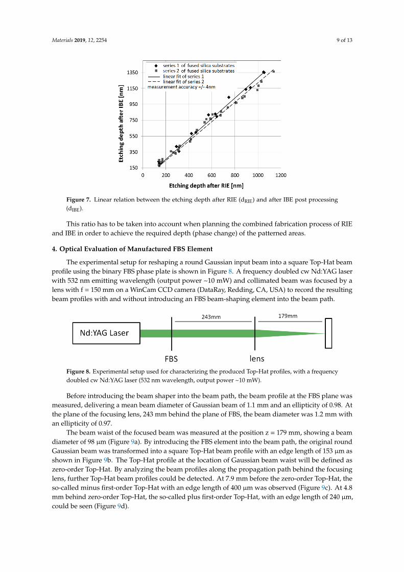
Figure 8. Experimental setup used for characterizing the produced Top-Hat profiles, with a frequency doubled cw Nd:YAG laser (532 nm wavelength, output power ~10 mW).
Before introducing the beam shaper into the beam path, the beam profile at the FBS plane was measured, delivering a mean beam diameter of Gaussian beam of 1.1 mm and an ellipticity of 0.98. At the plane of the focusing lens, 243 mm behind the plane of FBS, the beam diameter was 1.2 mm with an ellipticity of 0.97.
The beam waist of the focused beam was measured at the position z = 179 mm, showing a beam diameter of 98 µm (Figure 9a). By introducing the FBS element into the beam path, the original round Gaussian beam was transformed into a square Top-Hat beam profile with an edge length of 153 µm as shown in Figure 9b. The Top-Hat profile at the location of Gaussian beam waist will be defined as zero-order Top-Hat. By analyzing the beam profiles along the propagation path behind the focusing lens, further Top-Hat beam profiles could be detected. At 7.9 mm before the zero-order Top-Hat, the so-called minus first-order Top-Hat with an edge length of 400 µm was observed (Figure 9c). At 4.8 mm behind zero-order Top-Hat, the so-called plus first-order Top-Hat, with an edge length of 240 µm, could be seen (Figure 9d).
These experimental results confirm the principle design concept for the FBS beam shaper for the Top-Hat generation presented in this study. However, the measured +/− first order Top-Hat profiles behind and in front of the focal plane are not described by the design concept. Therefore, further investigations are necessary to understand these effects.
The generated zero-order Top-Hat (Figure 9b) is about 1.5 times bigger as the unshaped Gaussian intensity profile as expected. However, it exhibits a not completely flat center part. The intensity modulation is roughly ±5%. Furthermore, the energy fringes are roughly twice higher in comparison to the theoretical results shown in Figure 3c, leading to a lower efficiency of Top-Hat generation.
These energy fringes could cause unwanted heat transfer into the material. The authors got the feedback from an industrial partner that for a special semiconductor process the heat generated by these energy fringes lead to unwanted damage of the material. It depends on the application and the certain parameter set of pulse energy, pulse duration, material and wavelength if the beam shaping result generated by the FBS element is suitable. However, these energy fringes are typically far below the ablation threshold and are uncritical for the process [10].
Reasons for these deviations from the ideal Top-Hat profile could be non-ideal phase and amplitude distribution of used Gaussian beam, differences between theoretical and produced FBS surface, and aberration effects of focusing optic. Here, it will be necessary to carry out further investigations to understand the influence of theses parameter on the beam-shaping result.
Figure 8. Experimental setup used for characterizing the produced Top-Hat profiles, with a frequencydoubled cw Nd:YAG laser (532 nm wavelength, output power ~10 mW).
Before introducing the beam shaper into the beam path, the beam profile at the FBS plane wasmeasured, delivering a mean beam diameter of Gaussian beam of 1.1 mm and an ellipticity of 0.98. Atthe plane of the focusing lens, 243 mm behind the plane of FBS, the beam diameter was 1.2 mm withan ellipticity of 0.97.
The beam waist of the focused beam was measured at the position z = 179 mm, showing a beamdiameter of 98 µm (Figure 9a). By introducing the FBS element into the beam path, the original roundGaussian beam was transformed into a square Top-Hat beam profile with an edge length of 153 µm asshown in Figure 9b. The Top-Hat profile at the location of Gaussian beam waist will be defined aszero-order Top-Hat. By analyzing the beam profiles along the propagation path behind the focusinglens, further Top-Hat beam profiles could be detected. At 7.9 mm before the zero-order Top-Hat, theso-called minus first-order Top-Hat with an edge length of 400 µm was observed (Figure 9c). At 4.8mm behind zero-order Top-Hat, the so-called plus first-order Top-Hat, with an edge length of 240 µm,could be seen (Figure 9d).

Materials 2019, 12, 2254 10 of 13
Materials 2019, 12, x FOR PEER REVIEW 10 of 13
Figure 9. Measurement of generated beam profiles (a) Focused Gaussian profile at beam waist; (b) zero-order Top-Hat profile; (c) −1 order Top-Hat profile; (d) +1 order Top-Hat profile.
5. Conclusions
In this study, a design concept for a binary phase distribution with low periodicity and a central π-phase reversal is presented. This design transforms a Gaussian beam profile in the input plane into a square-shaped diffraction-limited Top-Hat beam profile in the far field. It was shown that 95% of the input energy can be transferred to the Top-Hat profile with a homogenous phase distribution. The calculated phase distribution of the so-called fundamental beam mode shaper (FBS) corresponds to an optical element showing just two different height levels. The height profile of the FBS is transferred in fused silica substrates by using microlithography, reactive ion etching (RIE) and ion beam etching (IBE). The RIE process generates an undesired nano surface roughness; therefore, IBE is used to smooth the surface. The experiments demonstrate a linear relation between the etching depth after RIE and IBE, leading to a depths ratio dIBE/dRIE of roughly 1.2. The optical evaluation of the manufactured FBS beam mode shaper confirms the presented concept design. In addition, it is shown that besides the Top-Hat profile in the focal plane (zero order), further Top-Hat profiles (+/− first order) occur along the propagation path behind the focusing lens. Further investigations are necessary to understand these effects.
Author Contributions: Conceptualization, C.B., E.J. and F.V.; methodology, C.B., U.R. and J.S.; software, C.B.; validation, C.B., F.V.; formal analysis, C.B.; investigation, C.B., J.S. and U.R.; resources, F.V., E.J. and U.U.; data curation, C.B., J.S. and F.V.; writing—original draft preparation, C.B.; writing—review and editing, F.V., A.F.L..; visualization, C.B., F.V.; supervision, F.V., A.F.L.; project administration, U.U., U.R. and A.F.L.; funding acquisition, U.U., U.R., C.B. and A.F.L.
Figure 9. Measurement of generated beam profiles (a) Focused Gaussian profile at beam waist;(b) zero-order Top-Hat profile; (c) −1 order Top-Hat profile; (d) +1 order Top-Hat profile.
These experimental results confirm the principle design concept for the FBS beam shaper for theTop-Hat generation presented in this study. However, the measured +/− first order Top-Hat profilesbehind and in front of the focal plane are not described by the design concept. Therefore, furtherinvestigations are necessary to understand these effects.
The generated zero-order Top-Hat (Figure 9b) is about 1.5 times bigger as the unshaped Gaussianintensity profile as expected. However, it exhibits a not completely flat center part. The intensitymodulation is roughly ±5%. Furthermore, the energy fringes are roughly twice higher in comparisonto the theoretical results shown in Figure 3c, leading to a lower efficiency of Top-Hat generation.
These energy fringes could cause unwanted heat transfer into the material. The authors got thefeedback from an industrial partner that for a special semiconductor process the heat generated bythese energy fringes lead to unwanted damage of the material. It depends on the application and thecertain parameter set of pulse energy, pulse duration, material and wavelength if the beam shapingresult generated by the FBS element is suitable. However, these energy fringes are typically far belowthe ablation threshold and are uncritical for the process [10].
Reasons for these deviations from the ideal Top-Hat profile could be non-ideal phase and amplitudedistribution of used Gaussian beam, differences between theoretical and produced FBS surface, andaberration effects of focusing optic. Here, it will be necessary to carry out further investigations tounderstand the influence of theses parameter on the beam-shaping result.

Materials 2019, 12, 2254 11 of 13
5. Conclusions
In this study, a design concept for a binary phase distribution with low periodicity and a centralπ-phase reversal is presented. This design transforms a Gaussian beam profile in the input plane into asquare-shaped diffraction-limited Top-Hat beam profile in the far field. It was shown that 95% of theinput energy can be transferred to the Top-Hat profile with a homogenous phase distribution. Thecalculated phase distribution of the so-called fundamental beam mode shaper (FBS) corresponds to anoptical element showing just two different height levels. The height profile of the FBS is transferredin fused silica substrates by using microlithography, reactive ion etching (RIE) and ion beam etching(IBE). The RIE process generates an undesired nano surface roughness; therefore, IBE is used to smooththe surface. The experiments demonstrate a linear relation between the etching depth after RIE andIBE, leading to a depths ratio dIBE/dRIE of roughly 1.2. The optical evaluation of the manufactured FBSbeam mode shaper confirms the presented concept design. In addition, it is shown that besides theTop-Hat profile in the focal plane (zero order), further Top-Hat profiles (+/− first order) occur alongthe propagation path behind the focusing lens. Further investigations are necessary to understandthese effects.
Author Contributions: Conceptualization, C.B., E.J. and F.V.; methodology, C.B., U.R. and J.S.; software, C.B.;validation, C.B., F.V.; formal analysis, C.B.; investigation, C.B., J.S. and U.R.; resources, F.V., E.J. and U.U.; datacuration, C.B., J.S. and F.V.; writing—original draft preparation, C.B.; writing—review and editing, F.V., A.F.L.;visualization, C.B., F.V.; supervision, F.V., A.F.L.; project administration, U.U., U.R. and A.F.L.; funding acquisition,U.U., U.R., C.B. and A.F.L.
Funding: This work was partially supported by German Federal Ministry of Education and Research (BMBF)through the project ‘NextGen-3DBat’, FKZ: 03XP0198B. The work of A.F.L. is also supported by the GermanResearch Foundation (DFG) under Excellence Initiative program by the German federal and state governments topromote top-level research at German universities.
Conflicts of Interest: The authors declare no conflict of interest. The funders had no role in the design of thestudy; in the collection, analyses, or interpretation of data; in the writing of the manuscript, or in the decision topublish the results.
References
1. Press Release, Laser Technologies for Semiconductor Manufacturing: A Massive Adoption, Extracted from:Laser Technologies for Semiconductor Manufacturing Report—Yole Développement, October 2017. Availableonline: http://www.yole.fr/LaserTechnologies_SemiManufacturing_MarketOverview.aspx#.XPbHeI_gpPY(accessed on 1 June 2019).
2. Urey, H. Spot size, depth-of-focus, and diffraction ring intensity formulas for truncated Gaussian beams.Appl. Opt. 2004, 43, 620–625. [CrossRef] [PubMed]
3. Raciukaitis, R.; Stankevicius, E.; Gecys, P.; Gedvilas, M.; Bischoff, C.; Jäger, E.; Umhofer, U.; Völklein, F. Laserprocessing by using diffractive optical laser beam shaping technique. JLMN 2011, 6, 1. [CrossRef]
4. Baird, B.; Gerke, T.; Wieland, K.; Paudel, N. P2 and P3 spatially shaped laser scribing of CdTe and a-Si thinfilm solar cells using a 532 nm picosecond MOFPA. In Proceedings of the 26th European Photovoltaic SolarEnergy Conference and Exhibition, Hamburg, Germany, 5–9 September 2011. [CrossRef]
5. Homburg, O.; Völkermeyer, F.; Toennissen, F.; Ganser, H.; Mitra, T. High-precision Gaussian-to-tophat beamtransformation improves structure quality and speed in micro-machining. In Proceedings of the FourthInternational WLT-Conference Lasers in Manufacturing, LIM 2007, Munich, Germany, 18–22 June 2007.
6. Chuang, H.; Lee, Y. Laser Scribing on Silver Flexible Substrate with Beam Shaping Technology. JLMN 2014,9, 3. [CrossRef]
7. Hahn, D.; Omenetto, N. Laser-induced breakdown spectroscopy (LIBS), part I, review of basic diagnosticsand plasma-particle interactions: Still-challenging issues within the analytical plasma community. Appl.Spectrosc. 2010, 64, 335–366. [CrossRef] [PubMed]
8. Tan, B.; Sivakumar, N.R.; Venkatakrishnan, K. Direct grating writing using femtosecond laser interferencefringes formed at the focal point. J. Opt. A Pure Appl. Opt. 2005, 7, 169–174. [CrossRef]
9. Rößler, F.; Kunze, T.; Lasagni, A.F. Fabrication of diffraction based security elements using direct laserinterference patterning. Opt. Exp. 2017, 25, 22959–22970. [CrossRef] [PubMed]

Materials 2019, 12, 2254 12 of 13
10. El-Khoury, M.; Voisiat, B.; Kunze, T.; Lasagni, A.F. Utilizing Fundamental Beam-Mode Shaping Techniquefor Top-Hat La-ser Intensities in Direct Laser Interference Patterning. JLMN 2018, 13, 3. [CrossRef]
11. Douglas, E.S.; Strahler, A.; Martel, J.; Cook, T.; Mendillo, C.; Marshall, R.; Chakrabarti, S.; Schaaf, C.;Woodcock, C.; Li, Z.; et al. DWEL: A dual-wavelength Echidna Lidar for ground based forest scanning. InProceedings of the IEEE IGARSS, Munich, Germany, 22–27 July 2012. [CrossRef]
12. Metel, A.S.; Stebulyanin, M.M.; Fedorov, S.V.; Okunkova, A.A. Power Density Distribution for LaserAdditive Manufacturing (SLM): Potential, Fundamentals and Advanced Applications. Technologies 2019, 7, 5.[CrossRef]
13. Rung, S.; Rexhepi, M.; Bischoff, C.; Hellmann, R. Laserscribing of Thin Films Using to p-Hat Laser BeamProfiles. JLMN 2013, 8, 3. [CrossRef]
14. Dickey, F.M. Laser Beam Shaping: Theory and Techniques, 2nd ed.; Marcel Dekker: New York, NY, USA, 2000;pp. 82–162.
15. Laskin, A.; Laskin, V. Variable beam shaping with using the same field mapping refractive beam shaper. InProceedings of the Laser Resonators, Microresonators, and Beam Control XIV, 82360D (2012), San Francisco,CA, USA, 21–26 January 2012; Volume 8236. [CrossRef]
16. Zimmermann, M.; Schmidt, M.; Bich, A.; Voelkel, R. Refractive Micro-optics for Multi-spot and Multi-lineGeneration. In Proceedings of the LPM 2008 9th International Symposium on Laser Precision Microfabrication,Quebec City, QC, Canada, 16–20 June 2008.
17. Veldkamp, W.B.; Kastner, C.J. Beam profile shaping for laser radars that use detector arrays. Appl. Opt. 1982,21, 345–356. [CrossRef]
18. Veldkamp, W.B. Laser beam profile shaping with interlaced binary diffraction gratings. Appl. Opt. 1982, 21,3209–3212. [CrossRef] [PubMed]
19. Gur, I.; Mendlovic, D. Diffraction limited domain flat-top generator. Opt. Commun. 1998, 145, 237–248.[CrossRef]
20. Yang, J.J.; Wang, M.R. Analysis and optimization on single-zone binary flat-top beam shaper. Opt. Eng. 2003,42, 3106–3113. [CrossRef]
21. Cordingley, J. Application of binary diffractive optic for beam shaping in semiconductor processing by lasers.Appl. Opt. 1993, 32, 2538–2542. [CrossRef] [PubMed]
22. de Saint Denis, R.; Passilly, N.; Laroche, M.; Mohammed-Brahim, T.; Aït-Ameur, K. Beam-shaping longitudinalrange of a binary diffractive optical element. Appl. Opt. 2006, 45, 8136–8142. [CrossRef]
23. Goodmann, J.W. Introduction to Fourier Optics, 2nd ed.; McGraw-Hill: New York, NY, USA, 1996; pp. 4–90.24. Hecht, E.; Schleitzer, A. Optik; De Gryuter: Berlin, Germany, 2014; pp. 839–930.25. Malitson, I.H. Interspecimen comparison of the refractive index of fused silica. J. Opt. Soc. Am. 1965, 55,
1205–1209. [CrossRef]26. Lee, R.E. Ion-Beam Etching (Milling). In VLSI Electronics Microstructure Science; Einspruch, N.G., Brown, D.M.,
Eds.; Academic Press: Cambridge, MA, USA, 1984; Volume 8, pp. 341–364.27. Schmitt, J.; Bischoff, C.; Rädel, U.; Grau, M.; Wallrabe, U.; Völklein, F. Enhancement of RIE: Etched Diffractive
Optical Elements surfaces by using Ion Beam Etching. In Proceedings of the SPIE Optical Systems Design,Jena, Germany, 7–10 September 2015. [CrossRef]
28. Leech, P.W. Reactive ion etching of quartz and silica-based glasses in CF4/CHF3 plasmas. Vacuum 1999, 55,191–196. [CrossRef]
29. Li, X.; Abe, T.; Esashi, E. Deep reactive ion etching of Pyrex glass using SF6 plasma. Sens. Actuators A Phys.2001, 87, 139–145. [CrossRef]
30. Akashi, T.; Yoshimura, Y. Deep reactive ion etching of borosilicate glass using an anodically bonded siliconwafer as an etch mask. J. Micromech. Microeng. 2006, 16, 1051–1056. [CrossRef]
31. Bertz, A.; Fendler, R.; Schuberth, R.; Hentsch, W.; Gessner, T.H. A New Method for High-Rate Deep DryEtching of Silicate Glass with Variable ETCH Profile. In Proceedings of the Solid-State Sensors, Actuatorsand Microsystems Conference, Lyon, France, 10–14 June 2007. [CrossRef]
32. Ray, T.; Zhu, H.; Meldrum, D.R. Deep reactive ion etching of fused silica using a single-coated soft masklayer for bio-analytical applications. J. Micromech. Microeng. 2010, 20, 097002. [CrossRef]
33. Tilli, M. Handbook of Silicon Based MEMS Materials and Technologies, 2nd ed.; Elsevier: Amsterdam, TheNetherlands, 2015; pp. 452–454.

Materials 2019, 12, 2254 13 of 13
34. Haefer, R.A. Oberflächen- und Dünnschicht-Technologie: Teil I: Beschichtungen von Oberflächen; Springer:Berlin/Heidelberg, Germany, 1987; pp. 95–120.
35. Wei, Q.; Li, K.-D.; Lian, J.; Wang, L. Angular dependence of sputtering yield of amorphous and polycrystallinematerials. J. Phys. D Appl. Phys. 2008, 41, 172002. [CrossRef]
36. Carter, G.; Nobes, M.; Katardjiev, I. The theory of ion beam polishing and machining. Vacuum 1993, 44,303–309. [CrossRef]
37. Li, Y.; Takino, H.; Frost, F. Ion beam planarization of diamond turned surfaces with various roughnessprofiles. Opt. Express 2017, 25, 7828–7838. [CrossRef] [PubMed]
38. Li, S.; Dai, Y. Ion Beam Figuring Technology. In Large and Middle-Scale Aperture Aspheric Surfaces: Lapping,Polishing, and Measurement; Wiley: Hoboken, NJ, USA, 2017; pp. 179–236.
39. Zhang, T.; Yi, F.; Wang, B.; Liu, J. Sidewall smoothing of micro-pore optics by ion beam etching. Surf. Coat.Technol. 2015, 278, 127–131. [CrossRef]
© 2019 by the authors. Licensee MDPI, Basel, Switzerland. This article is an open accessarticle distributed under the terms and conditions of the Creative Commons Attribution(CC BY) license (http://creativecommons.org/licenses/by/4.0/).


![Superconducting RF Activities at Cornell University · equipped with high power fundamental and higher order mode couplers[2]. Upto 12 ma of beam current was held in the stonfge ring](https://static.fdocuments.net/doc/165x107/5f2cfdde2f9be37a67670a84/superconducting-rf-activities-at-cornell-university-equipped-with-high-power-fundamental.jpg)
![Design of Beam Column [Compatibility Mode]](https://static.fdocuments.net/doc/165x107/54730b6bb4af9f2b058b45b2/design-of-beam-column-compatibility-mode-55845af2cac52.jpg)
![OWA010010 WCDMA RAN Fundamental ISSUE 1.111 [Compatibility Mode]](https://static.fdocuments.net/doc/165x107/577cd45c1a28ab9e7898504e/owa010010-wcdma-ran-fundamental-issue-1111-compatibility-mode.jpg)