DESIGN AND IMPLEMENT - Washington University in St. Louis · DESIGN AND IMPLEMENT A TION OF A MUL...
166
Transcript of DESIGN AND IMPLEMENT - Washington University in St. Louis · DESIGN AND IMPLEMENT A TION OF A MUL...

c� Copyright by John William Lockwood� ����

DESIGN AND IMPLEMENTATION OF A MULTICAST�INPUT�BUFFERED ATM SWITCH FOR THE IPOINT TESTBED
BY
JOHN WILLIAM LOCKWOOD
B�S�� University of Illinois� ����M�S�� University of Illinois� ����
THESIS
Submitted in partial fulllment of the requirementsfor the degree of Doctor of Philosophy in Electrical Engineering
in the Graduate College of theUniversity of Illinois at Urbana�Champaign� ���
Urbana� Illinois

DESIGN AND IMPLEMENTATION OF A MULTICAST�INPUT�BUFFERED ATM SWITCH FOR THE IPOINT TESTBED
John William Lockwood� PhDDepartment of Electrical and Computer EngineeringUniversity of Illinois at Urbana�Champaign� ���
Sung Mo Kang� Advisor
This thesis presents the design and implementation of the multicast� input�bu�ered
Asynchronous Transfer Mode �ATM switch for use with the iPOINT testbed� The
input�bu�ered architecture of this switch is optimal in terms of the memory bandwidth
required for the implementation of an ATM queue module� The contention resolution
algorithm used by the iPOINT switch supports atomic multicast� enabling the simulta�
neous delivery of ATM cells to multiple output ports without the need for recirculation
bu�ers� duplication of cells in memory� or multiple clock cycles to transfer a cell from an
input queue module�
The implementation of the prototype switch is unique in that it was entirely con�
structed using Field Programmable Gate Array �FPGA technology� A fully functional�
ve�port� ��� Mbps ATM switch has been developed and currently serves as the high�
speed� optically interconnected� local area network for a cluster of Sun SPARCstations
and the gateway to the wide�area Blanca�XUNET gigabit testbed� Through the use of
FPGA technology� new hardware�based switching algorithms and functionality can be
implemented without the need to modify hard�wired logic� Further� through the use of
the remote switch manager� switch controller� and FPGA controller� the management�
operation� and even logic functionality of the iPOINT testbed can be dynamically altered�
all without the need for physical access to the iPOINT hardware�
Based on the existing prototype switch� the design of the FPGA�based� gigabit�per�
second �Any�Queue� module is presented� For this design in its maximum congura�
tion� up to �� queue modules can be supported� providing an aggregate throughput of
iii

��� Gbps� Further� the design of a ��port� ���� Gbps aggregate throughput� switch
fabric is documented that can be entirely implemented using only eight FPGA devices�
In addition to the design of the switch module� this thesis describes the supporting
components of the iPOINT testbed� including the network control and application soft�
ware� the hardware specications of the switch interface� and the device requirements of
the optoelectronic components used in the testbed�
iv

ACKNOWLEDGMENTS
I would like to thank my advisor� Professor Sung Mo Kang� who has supported and
encouraged the research of the iPOINT testbed from the project�s inception in �����
Professor Kang has stressed the importance of system design�that is� a complete de�
sign that can leverage the benets of both optoelectronic and VLSI technologies� In
addition to Professor Kang� I would like to thank the other members of my commit�
tee� Professor Roy Campbell and Professor Steve Bishop� The iPOINT project involves
interdisciplinary research of electronic circuit design� network computing� and optoelec�
tronic systems� Professor Campbell�s experience with ATM networks� computer systems�
and his initial research on the Pulsar switch architecture has been instrumental in this
work� Professor Bishop�s direction of the Center for Compound Semiconductor Micro�
electronics and discussions of optical and OEIC devices enabled the development and
implementation of the laser and optoelectronic components used for this testbed�
I would like to thank Charles Kalmanek of AT�T Bell Laboratories for his thoughtful
discussions of the requirements of ATM switches and systems for use in the wide�area
network and for the opportunity to intern at Bell Labs� I would also like to thank other
members of the XUNET research group� including William Marshall� Robert Restrick�
and Srinivasan Keshav for their discussions and comments with respect to the develop�
ment of the XUNET hardware and software�
I would like to thank the other members of the iPOINT research group� including
Haoran Duan and Ashfaq Hossain� Haoran Duan�s dedication and work on the iPOINT
queue module and trunk port have been a key factor in the success of this project� Ashfaq
Hossain�s work on the iPOINT video server remains the primary source of tra�c on the
iPOINT switch� I would like to thank all of my undergraduate students who have each
contributed to various parts of the project� in particular� Masood Makkar for his work
v

on the switch management hardware� Ben Cox for his work on the kernel�level device
driver� and Je�rey Will for his work on the FPGA demultiplexor circuit�
I would also like to thank Jim Morikuni for his insightful discussions on the design
of OEIC components for use with the testbed� Pablo Mena for his helpful conversations
on contention graph algorithms� and Brent Whitlock for his work on the iFROST link
simulator� In addition to the members of our research group� I would like to thank
Professor George Papen and Matt Bruensteiner for their work on the optical subsystems
and eye�pattern measurements needed for the iPOINT trunk port�
This work was supported by the National Science Foundation Engineering Research
Center grant ECD ������� the Advanced Research Program Agency �ARPA grant for
the Center for Optoelectronic Science and Technology �COST � MDA �������������� and
the AT�T Foundation grant�
vi

TABLE OF CONTENTS
CHAPTER PAGE
� INTRODUCTION � � � � � � � � � � � � � � � � � � � � � � � � � � � � � � � � �
� QUEUEING FOR ATM SWITCHES � � � � � � � � � � � � � � � � � � � � ���� ATM Design Constraints � � � � � � � � � � � � � � � � � � � � � � � � � � � ���� Queueing � � � � � � � � � � � � � � � � � � � � � � � � � � � � � � � � � � �
����� Shared queueing � � � � � � � � � � � � � � � � � � � � � � � � � � � ������ Output queueing � � � � � � � � � � � � � � � � � � � � � � � � � � � ������ Input queueing � � � � � � � � � � � � � � � � � � � � � � � � � � � � ������ FIFO input queueing � � � � � � � � � � � � � � � � � � � � � � � � � ������ Non�FIFO input queueing � � � � � � � � � � � � � � � � � � � � � � ��
��� Hybrid Queueing � � � � � � � � � � � � � � � � � � � � � � � � � � � � � � � ������� Input�output queueing � � � � � � � � � � � � � � � � � � � � � � � � ������� Crosspoint queueing � � � � � � � � � � � � � � � � � � � � � � � � � ������� Banyon�based internal queueing � � � � � � � � � � � � � � � � � � � ������� Scalability � � � � � � � � � � � � � � � � � � � � � � � � � � � � � � � ��
� MULTICAST CONTENTION RESOLUTION ALGORITHMS � � � ���� Cell Scheduling for Input�Bu�ered ATM Switches � � � � � � � � � � � � � ��
����� Atomic multicast � � � � � � � � � � � � � � � � � � � � � � � � � � � ������� Unicast contention resolution � � � � � � � � � � � � � � � � � � � � ������� Multiple choice per port �MCPP � � � � � � � � � � � � � � � � � � ������� Single choice per port �SCPP � � � � � � � � � � � � � � � � � � � � ��
��� iPOINT Multicast Contention Resolution Algorithm � � � � � � � � � � � � ������� iMCRA implementation � � � � � � � � � � � � � � � � � � � � � � � ������� iMCRA fairness � � � � � � � � � � � � � � � � � � � � � � � � � � � � ������� iMCRA simulation results � � � � � � � � � � � � � � � � � � � � � � ��
� iPOINT PROJECT PHASES � � � � � � � � � � � � � � � � � � � � � � � � � ����� Phase I� ATM Software Development � � � � � � � � � � � � � � � � � � � � ��
����� ATM diagnostic software � � � � � � � � � � � � � � � � � � � � � � � ������� User�space ATM application software � � � � � � � � � � � � � � � � ������� Kernel�space ATM device driver � � � � � � � � � � � � � � � � � � � ������� Benchmarking of the SBA���� host adapter � � � � � � � � � � � � ��
��� Phase II� FPGA Prototype Switch � � � � � � � � � � � � � � � � � � � � � � ������� The iPOINT queueing module � � � � � � � � � � � � � � � � � � � � ������� The iPOINT switch module � � � � � � � � � � � � � � � � � � � � � ��
��� Phase III� iPOINT�XUNET Internetworking � � � � � � � � � � � � � � � ������� Wide�area network benchmarking � � � � � � � � � � � � � � � � � � ��
vii

����� TCP�IP�over�ATM experiments � � � � � � � � � � � � � � � � � � � ������� UDP�IP�over�ATM experiments � � � � � � � � � � � � � � � � � � � ��
��� Phase IV� � Gbps Networking with UIUC Devices � � � � � � � � � � � � � ������� OEIC laser driver and optical receiver specications � � � � � � � � ������� An analysis of �B���B encoded data � � � � � � � � � � � � � � � � ������� iPOINT trunk port � � � � � � � � � � � � � � � � � � � � � � � � � � ������� Fiber�optic link experiment � � � � � � � � � � � � � � � � � � � � � ��
��� Phase V� Total Remote Operation � � � � � � � � � � � � � � � � � � � � � � ������� The iPOINT switch controller � � � � � � � � � � � � � � � � � � � � ������� Switch manager � � � � � � � � � � � � � � � � � � � � � � � � � � � � ������� FPGA download controller � � � � � � � � � � � � � � � � � � � � � � ��
�� Phase VI� Multi�Gbps Networking � � � � � � � � � � � � � � � � � � � � � � ��
� THE iPOINT TESTBED � � � � � � � � � � � � � � � � � � � � � � � � � � � ����� iPOINT Switch Module � � � � � � � � � � � � � � � � � � � � � � � � � � � �
����� Layout of the switch module � � � � � � � � � � � � � � � � � � � � � ������� Displays and switches � � � � � � � � � � � � � � � � � � � � � � � � � ��
��� The iPOINT FPGA Prototype Switch � � � � � � � � � � � � � � � � � � � ������� Circuit design techniques and constraints � � � � � � � � � � � � � � ������� Top�level design � � � � � � � � � � � � � � � � � � � � � � � � � � � � ������� Timing control � � � � � � � � � � � � � � � � � � � � � � � � � � � � ������� Ports � � � � � � � � � � � � � � � � � � � � � � � � � � � � � � � � � � ������� Trunk interface � � � � � � � � � � � � � � � � � � � � � � � � � � � � ������ iPOINT Multicast Contention Resolution Algorithm �iMCRA � � ������� Master switch � � � � � � � � � � � � � � � � � � � � � � � � � � � � � ������� ATM cell ROM � � � � � � � � � � � � � � � � � � � � � � � � � � � � ������� Operational switches � � � � � � � � � � � � � � � � � � � � � � � � � ������� Switch management unit � � � � � � � � � � � � � � � � � � � � � � � �������� Microprocessor interface � � � � � � � � � � � � � � � � � � � � � � � ������� Completed FPGA design � � � � � � � � � � � � � � � � � � � � � � � �
��� iPOINT Switch Controller � � � � � � � � � � � � � � � � � � � � � � � � � � ������ Switch control circuit � � � � � � � � � � � � � � � � � � � � � � � � � ������ Translation table updating � � � � � � � � � � � � � � � � � � � � � � ������ Operation of the VPIVCI program � � � � � � � � � � � � � � � � � ������ Running TCP�IP�over�ATM on the iPOINT switch � � � � � � � �
��� FPGA Controller � � � � � � � � � � � � � � � � � � � � � � � � � � � � � � � ������ Control software � � � � � � � � � � � � � � � � � � � � � � � � � � � ������ Default design les � � � � � � � � � � � � � � � � � � � � � � � � � � �
� ATM HARDWARE INTERFACE � � � � � � � � � � � � � � � � � � � � � � ���� Electrical Interface to the iPOINT ��� Mbps Port � � � � � � � � � � � � � ���� Logical Interface to the iPOINT Switch � � � � � � � � � � � � � � � � � � � ���� The ATM Phone � � � � � � � � � � � � � � � � � � � � � � � � � � � � � � � ��
���� ATM phone protocol � � � � � � � � � � � � � � � � � � � � � � � � � ��
viii

���� ATM phone FPGA logic � � � � � � � � � � � � � � � � � � � � � � � ������ ATM phone hardware components � � � � � � � � � � � � � � � � � ����� ATM phone workstation software � � � � � � � � � � � � � � � � � � ������ Possible enhancements to the ATM phone � � � � � � � � � � � � � ��
�� Wireless ATM Interfacing to the iPOINT Switch � � � � � � � � � � � � � � ��
� MULTICAST NETWORKS � � � � � � � � � � � � � � � � � � � � � � � � � � ����� IP Multicast � � � � � � � � � � � � � � � � � � � � � � � � � � � � � � � � � � ��
����� The Multicast Backbone �MBone � � � � � � � � � � � � � � � � � � ������� IP multicast over ATM � � � � � � � � � � � � � � � � � � � � � � � � ��
��� ATM Multicast � � � � � � � � � � � � � � � � � � � � � � � � � � � � � � � � ������� Multicast signalling � � � � � � � � � � � � � � � � � � � � � � � � � � ������� Multicast service model � � � � � � � � � � � � � � � � � � � � � � � ��
THE MULTIGIGABITPERSECOND iPOINT SWITCH � � � � � � ����� Multigigabit�per�second ATM Switch Port � � � � � � � � � � � � � � � � � ���� The Any�Queue Module � � � � � � � � � � � � � � � � � � � � � � � � � � � ��
����� The VPI�VCI�management table � � � � � � � � � � � � � � � � � � ������� Cell processing � � � � � � � � � � � � � � � � � � � � � � � � � � � � ������� Queueing structure � � � � � � � � � � � � � � � � � � � � � � � � � � ��
��� The Distributed iMCRA � � � � � � � � � � � � � � � � � � � � � � � � � � � ������� Slot usage of the distributed iMCRA � � � � � � � � � � � � � � � � ������� Atomic and nonatomic multicast � � � � � � � � � � � � � � � � � � ������ Multiple choice per port � � � � � � � � � � � � � � � � � � � � � � � ������ Prioritized switching � � � � � � � � � � � � � � � � � � � � � � � � � ��
��� Switching Fabrics � � � � � � � � � � � � � � � � � � � � � � � � � � � � � � � ������� FPGA switch fabric � � � � � � � � � � � � � � � � � � � � � � � � � � ������� Pulsar ring switch fabric � � � � � � � � � � � � � � � � � � � � � � � ���
� ACCOMPLISHMENTS AND FUTURE RESEARCH � � � � � � � � � ������ Summary of Accomplishments � � � � � � � � � � � � � � � � � � � � � � � � ������ Future Research � � � � � � � � � � � � � � � � � � � � � � � � � � � � � � � � ��
APPENDIX A� iMCRA SIMULATOR � � � � � � � � � � � � � � � � � � ���A�� iMCRA C�� Source Code � � � � � � � � � � � � � � � � � � � � � � ���A�� iMCRA Sample Output � � � � � � � � � � � � � � � � � � � � � � � ���
APPENDIX B� ATM CELLLEVEL TESTING PROGRAM � � � � ���
APPENDIX C� iPOINT SWITCH SCHEMATICS � � � � � � � � � � � ���
APPENDIX D� iMCRA IMPLEMENTATION � � � � � � � � � � � � � ���D�� iMCRA� VHDL Entity � � � � � � � � � � � � � � � � � � � � � � � � ���D�� iMCRA� VHDL Architecture � � � � � � � � � � � � � � � � � � � � � ���
ix

APPENDIX E� VPIVCI SWITCH CONTROLLER � � � � � � � � � � ���
APPENDIX F� FPGA CONTROLLER � � � � � � � � � � � � � � � � � � ���F�� Include File � � � � � � � � � � � � � � � � � � � � � � � � � � � � � � ���F�� S�TCP Program � � � � � � � � � � � � � � � � � � � � � � � � � � � � ���F�� R�TCP Program � � � � � � � � � � � � � � � � � � � � � � � � � � � ���
APPENDIX G� ATM TELEPHONE � � � � � � � � � � � � � � � � � � � � ���G�� FPGA Circuit Modication � � � � � � � � � � � � � � � � � � � � � ���G�� Multimedia Workstation Application Software � � � � � � � � � � � ��
REFERENCES � � � � � � � � � � � � � � � � � � � � � � � � � � � � � � � � � ���
VITA � � � � � � � � � � � � � � � � � � � � � � � � � � � � � � � � � � � � � � � ���
x

LIST OF FIGURES
Figure Page
��� The role of optical components in high�speed networks� � � � � � � � � � � �
��� The ATM cell format� � � � � � � � � � � � � � � � � � � � � � � � � � � � � ���� Queue congurations� � � � � � � � � � � � � � � � � � � � � � � � � � � � � � ���� Cell loss of FIFO queues with bursty tra�c� � � � � � � � � � � � � � � � � ���� Hybrid queue congurations� � � � � � � � � � � � � � � � � � � � � � � � � � ����� Internal queue congurations� � � � � � � � � � � � � � � � � � � � � � � � � ��
��� Cell scheduling for input�bu�ered ATM switches� � � � � � � � � � � � � � ���� Contention resolution graph� � � � � � � � � � � � � � � � � � � � � � � � � � ����� Multicast subset decomposition� � � � � � � � � � � � � � � � � � � � � � � � ����� Unicast subset decomposition� � � � � � � � � � � � � � � � � � � � � � � � � ����� Single choice per port decomposition� � � � � � � � � � � � � � � � � � � � � ���� Vertex cover problem for SCPP� � � � � � � � � � � � � � � � � � � � � � � � ����� Example of the iMCRA algorithm� � � � � � � � � � � � � � � � � � � � � � ����� Simulation results of the iMCRA algorithm� � � � � � � � � � � � � � � � � ��
��� Point�to�point ATM networking� � � � � � � � � � � � � � � � � � � � � � � � ����� SBA���� throughput with UIUC STREAMS module� � � � � � � � � � � � ����� Photograph of the iPOINT switch� queue� and optic modules� � � � � � � ����� Internetworking of iPOINT switch and XUNET wide�area network� � � � ����� Wide�area network IP�over�ATM benchmarking results� � � � � � � � � � � ���� Mean optical power specications for iPOINT OEIC devices� � � � � � � � ����� Fourier analysis with bandpass constraints� � � � � � � � � � � � � � � � � � ����� iPOINT trunk port� � � � � � � � � � � � � � � � � � � � � � � � � � � � � � � ����� Photograph of the ber�optic link experiment� � � � � � � � � � � � � � � � ������ Hierarchical interconnection of the iPOINT switch� � � � � � � � � � � � � ��
��� iPOINT testbed components� � � � � � � � � � � � � � � � � � � � � � � � � ����� iPOINT switch module� � � � � � � � � � � � � � � � � � � � � � � � � � � � ���� Photograph of the iPOINT switch module� � � � � � � � � � � � � � � � � � ����� Design hierarchy of the iPOINT switch� � � � � � � � � � � � � � � � � � � � ����� Channel mapping for trunk port destinations� � � � � � � � � � � � � � � � ���� Contents of on�chip ATM cell ROM � � � � � � � � � � � � � � � � � � � � � ���� Operation modes of the iPOINT switch � � � � � � � � � � � � � � � � � � � ���� Switch management circuit� � � � � � � � � � � � � � � � � � � � � � � � � � ����� Terminal display generated by switch management hardware � � � � � � � ������ Routed and placed iPOINT switch FPGA� � � � � � � � � � � � � � � � � � ����� iPOINT switch controller� � � � � � � � � � � � � � � � � � � � � � � � � � � �
xi

���� Controller�to�FPGA packet format � � � � � � � � � � � � � � � � � � � � � ����� Command syntax for a single virtual circuit � � � � � � � � � � � � � � � � ����� Example of creating a single virtual circuit � � � � � � � � � � � � � � � � � ����� Full virtual circuit connectivity example� � � � � � � � � � � � � � � � � � � ���� VPIVCI conguration le �vlist�demo � � � � � � � � � � � � � � � � � � ���� Enabling TCP�IP�over�ATM for use with iPOINT switch � � � � � � � � � ���� A �ping� command sent via the iPOINT switch � � � � � � � � � � � � � � ����� iPOINT FPGA design circuits � � � � � � � � � � � � � � � � � � � � � � � � ����� FPGA controller diagram� � � � � � � � � � � � � � � � � � � � � � � � � � � ����� Photograph of the iPOINT FPGA controller� � � � � � � � � � � � � � � � � �
�� ��� Mbps port I�O interface� � � � � � � � � � � � � � � � � � � � � � � � � � ���� Switch�queue timing specications� � � � � � � � � � � � � � � � � � � � � � ���� Format of the control word� � � � � � � � � � � � � � � � � � � � � � � � � � ���� The iPOINT ATM phone� � � � � � � � � � � � � � � � � � � � � � � � � � � ���� ATM phone modied port I�O interface� � � � � � � � � � � � � � � � � � � ��� Photograph of the completed ATM phone� � � � � � � � � � � � � � � � � � ��
��� IP multicast routing in the extended LAN� � � � � � � � � � � � � � � � � � ����� Virtual circuit usage for multicast� � � � � � � � � � � � � � � � � � � � � � ��
��� iPOINT multigigabit switch modules� � � � � � � � � � � � � � � � � � � � � ����� The Any�Queue module� � � � � � � � � � � � � � � � � � � � � � � � � � � � ����� Contents of the VPI�VCI�management table� � � � � � � � � � � � � � � � ����� Per�virtual circuit queueing using linked lists� � � � � � � � � � � � � � � � ����� Distributed iMCRA algorithm� slot usage� � � � � � � � � � � � � � � � � � ���� FPGA device usage for small iPOINT switches � � � � � � � � � � � � � � � ����� Switch fabric for ��port FPGA switch ���bit slice � � � � � � � � � � � � � ������ Parallel shift register ring switch fabric� � � � � � � � � � � � � � � � � � � � ������ Pulsar circuit boards� � � � � � � � � � � � � � � � � � � � � � � � � � � � � � ���
C�� Top level switch �sw��ttm � � � � � � � � � � � � � � � � � � � � � � � � � � ���C�� Switch management unit �management � � � � � � � � � � � � � � � � � � � ���C�� Timing control �timingctrl � � � � � � � � � � � � � � � � � � � � � � � � � � ���C�� Rom cell �romcell � � � � � � � � � � � � � � � � � � � � � � � � � � � � � � � ���C�� Microprocessor interface �uproc � � � � � � � � � � � � � � � � � � � � � � � ���C� Master switch �masterswitch � � � � � � � � � � � � � � � � � � � � � � � � � ���C�� Switching element �FPGASwitch � � � � � � � � � � � � � � � � � � � � � � � ���C�� Switching primitive ���switch � � � � � � � � � � � � � � � � � � � � � � � � ���C�� Logical trunk port control �portT � � � � � � � � � � � � � � � � � � � � � � ���C��� Physical trunk port I�O �trunkport � � � � � � � � � � � � � � � � � � � � � ���C��� Logical port control �portc � � � � � � � � � � � � � � � � � � � � � � � � � � ��C��� Physical port I�O �portPB � � � � � � � � � � � � � � � � � � � � � � � � � � ���C��� Physical port I�O �portPL � � � � � � � � � � � � � � � � � � � � � � � � � � ���
xii

C��� Physical port I�O �portPR � � � � � � � � � � � � � � � � � � � � � � � � � � ���C��� Physical port I�O �portPT � � � � � � � � � � � � � � � � � � � � � � � � � � ���
G�� ATM telephone port I�O �portPBp � � � � � � � � � � � � � � � � � � � � � ���G�� ATM telephone port control �portaudio � � � � � � � � � � � � � � � � � � � ���
xiii

CHAPTER �
INTRODUCTION
The exponential growth of the Internet suggests a great opportunity for networking
of desktop workstations and personal computers� Network�based applications such as the
World Wide Web �WWW � desktop video conferencing� distributed computing� shared
le systems� and remote access to supercomputing resources have dramatically increased
the demand for high�speed networks�
The demand for increased bandwidth can be satised through the use of optical� elec�
tronic� and mixed optoelectronic devices� As shown in Figure ���� these components have
utility for a broad range of telecommunication and data communication systems� Wave�
length Division Multiplexing �WDM provides an e�cient mechanism for maximizing
the bandwidth of long�haul links by multiplexing multiple channels onto a single ber�
Time�division multiplexing �TDM provides the means for combining many slower data
streams into a single� faster bit�rate channel�
The focus of this research� however� is on the darkened components of Figure ����
These components are those elements of the network that involve data communications
and tra�c sources that do not produce constant bit�rate data streams� For data com�
munications where tra�c is bursty� statistical multiplexing is required� Asynchronous
Transfer Mode �ATM provides this functionality and promises to become the standard
for future high�speed networks� For ATM switching� cell bu�ering and header translation
are required� which in turn necessitate the use of mixed optoelectronic� rather than all
optical components� This thesis describes the design and implementation of the iPOINT
switch and supporting components of the iPOINT testbed�
Chapter � begins by describing Asynchronous Transfer Mode �ATM and discussing
the design constraints imposed by the ATM protocol� Various mechanisms for cell queue�
ing are discussed� and it is explained why input queueing was chosen for use with the
iPOINT testbed�
�

AdapterHIPPI/ATM
(NCSA)Supercomputers Switche
Ethernet LAN
ATM
ATMSwitch
Cellular
LANWireless
Multi-Gb/s
ATM Switch
ATM Switch
...
PBX
ServiceConstant Bit-Rate
...
...
Desktop ATM
OEIC
Network/VideoFile Server Workstations
...
Desktop ATM Workstations
OEICs
Short-haulfiber links
Phone service
SONET TDM
DS1
DS3
OC12
Figure ��� The role of optical components in high�speed networks�
Chapter � discusses cell scheduling for input�bu�ered ATM switches� In particular�
it examines multicast cell scheduling for the case when an input cell is simultaneously
delivered to multiple output ports� The iPOINT Multicast Contention Resolution Algo�
rithm �iMCRA is introduced� and a discussion of the characteristics of this algorithm
are provided� A simulation shows that the iMCRA provides near�optimal performance
using only minimal hardware�
Chapter � provides a chronology of the iPOINT project� It rst discusses the software
programs and network device drivers developed for the initial phase of point�to�point
networking of the desktop workstations� The chapter next introduces the iPOINT switch
and queue modules but leaves the details of the switch implementation for Chapter �� It
then describes the interconnection of the iPOINT testbed to the XUNET testbed and
provides the results of end�to�end performance measurements of IP�over�ATM tra�c both
for the the local testbed and for the wide�area network� The chronology continues by
�

discussing how the iPOINT trunk port integrated the optoelectronic devices fabricated
by the UIUC microelectronics center into the existing testbed� It continues by discussing
why and how complete remote operation of the iPOINT testbed is possible� The chapter
concludes by discussing the current phase of the iPOINT project� which involves the
design of the multi gigabit�per�second� FPGA�based� distributed switch�
Chapter � provides the details of the iPOINT switch implementation� The purpose
of this chapter is twofold� First� it serves as a user�s guide to the operation and man�
agement of the existing testbed� It describes how to create and modify virtual circuits�
how to download new FPGA designs� and how to monitor and control the operation
of the iPOINT switch� Second� the chapter fully documents the design of the iPOINT
switch� In particular� it discusses the VHDL and the schematic implementation of each
component and subcomponent of the iPOINT switch� In conjunction with Appendix C
and Appendix D� the design of a complete ATM switch is released to the public domain�
Chapter details how external hardware can be attached directly to the iPOINT
switch via the ��� Mbps switch port interface� By means of the ATM telephone example�
it shows how the FPGA logic can be customized to simplify the design of the external
logic� The chapter concludes with a brief discussion of how this port could be used to
implement an ATM base station for a wireless LAN�
Chapter � brie�y digresses from the hardware implementation of the iPOINT switch
to discuss the establishment of multicast virtual circuits� The current state of IP�based
multicast routing on extended LANs is discussed� It is shown that current ATMmulticast
signalling protocol is inadequate� as it lacks the mechanisms for leaf�initiated joins and
for user authentication� The Simple Multicast ATM for XUNET �SMAX model for
multicast signalling is brie�y summarized�
Chapter � discusses the current research of the iPOINT testbed� namely the devel�
opment of a multi gigabit�per�second� distributed ATM switch� The design retains the
key features of the iPOINT testbed�the use of input queueing to minimize memory
bandwidth� support for atomic multicast cell transmission� and �exibility of operation
through the use of FPGA technology� The design of the Any�Queue module is presented�
�

Through the use of an FPGA�based cell processor� the Any�Queue module can support
a wide range of queueing service disciplines� including the per�virtual circuit� prioritized�
round�robin service discipline� The operation of the distributed iMCRA using the hard�
ware of the Any�Queue module is described� It is shown how a switch with up to ��
ports can be scheduled to provide an aggregate throughput of ��� Gbps� The chapter
concludes by describing a ��port� ���� Gbps aggregate throughput switch fabric that
can be entirely implemented using only eight FPGA devices�
�

CHAPTER �
QUEUEING FOR ATM SWITCHES
Asynchronous Transfer Mode �ATM technology meets the demands of present and
future multi gigabit�per�second computer networks because it o�ers low�latency� high�
bandwidth� and asynchronously multiplexed data switching ���� Circuit�based switching
is ill�suited for the transmission of bursty data and compressed video streams because it
deterministically allocates network resources� ATM�based switching� however� can asyn�
chronously multiplex up to ��� individual connections per link without dedicating bers�
wavelengths� or time slots to idle or intermittent data sources� The short length of the
ATM cell is well�suited for multimedia� distributed computing� and real�time applications
where message latency is critical�
��� ATM Design Constraints
The ATM protocol imposes specic requirements on the design of the switch in terms
of the cell length� header translation� and cell ordering ���� The format of an ATM cell
is shown in Figure ���� Each cell is �� bytes long� including the four�byte cell header� a
single�byte header checksum� and a ���byte data payload� Unlike protocols such as HIPPI
GFC: Generic Flow Control [4 bits] (UNI)
VPI: Virtual Path Identifier [8/12 bits]
CLP: Cell Loss Priority [1 bit]
VCI: Virtual Circuit Identifier [16 bits]
PT: Payload Type [3 bits]
HEC: Header Error Check [8 bits]
Payload: [48 Bytes]Payload
CLP
HEC
VCI
GFC/VPI VPI...
53 Bytes
PT
Figure ��� The ATM cell format�
�

or Fiber�channel� which assume that a large amount of data will be transferred within a
single transaction� a high�bandwidth ATM switch must provide high cell throughput�
The ATM cell header includes the Virtual Path Identier �VPI and the Virtual
Circuit Identier �VCI to identify those cells which belong to specic connections� In
general� a connection is routed through multiple ATM switches in the network� To avoid
global name allocation� the value of a given connection�s VPI and VCI may di�er on
each physical link of the network� As such� an ATM switch must be able to modify the
contents of the cell header� Because the cell is modied� it is not possible to build a true
ATM switch using only passive optical waveguides�
When two or more cells are to be switched to the same destination port� only one cell
can be transmitted� The other cells must be dropped� de�ected� or queued� The dropping
of a single ATM cell causes the retransmission of an entire message �AAL� frame � which
in turn introduces end�to�end ine�ciency and performance degradation� The de�ection
of an ATM cell to an alternate route is unacceptable� as an ATM switch is expected to
preserve the order of the transmitted cells for each virtual circuit� Techniques such as
hot�potato routing violate this ordering constraint because cells routed along a shorter
path may arrive before an earlier cell that was routed along a longer path ���� An ATM
switch� therefore� must provide cell queueing� At present� optical storage technologies do
not o�er the economy or capacity of silicon�based Random Access Memory �RAM �
To meet the requirements listed above� the iPOINT testbed is implemented with
optoelectronic components� enabling the maximal use of both photonic and electronic
technologies� Photonic components excel in terms of data transfer and minimal crosstalk�
while electronic components e�ciently provide cell storage and header translation�
��� Queueing
As shown in Figure ���� a single�stage ATM switch can queue data though the use of
a common pool of shared memory� by queueing at the output ports� or by queueing at
the input ports�

Queue
Queue
Queue
QueueQueue
Queue
Queue
Shared Queue Output Queueing
... ...
Input Queueing
Figure ��� Queue congurations�
����� Shared queueing
Due to the rather short length of the ATM cell� the bandwidth of a shared memory
switch is fundamentally limited by the cycle time of the RAM� Using the largest possible
memory width �one cell wide � a minimum of two memory operations is required per
cell �one read and one write � Using a RAM with a �� ns cycle time� a simple shared
memory switch is limited to switching only ����� ns � � � �� million cells per second�
thus limiting the aggregate throughput of the switch to � Gbps� Although a slightly
faster switch can be built using fast� static RAM� it incurs additional expense and has a
limited bu�er size ����
����� Output queueing
The aggregate throughput of an output�queued switch is also fundamentally limited
by memory bandwidth� In the worst case� an output queue will receive cells from every
input port simultaneously� which again requires a bu�er with a memory bandwidth equal
to the aggregate throughput of the switch� In ���� it was shown that for random tra�c�
an output queue capable of receiving at least eight cells simultaneously could provide
an acceptable cell loss probability�comparable to the probability of the link�s Bit Error
Rate �BER corrupting the cell due to at least a one�bit error of the data within the
ATM cell� Although this provides an improvement in terms of the memory bandwidth
requirement� it still requires that the memory bandwidth be a large multiple of the link
rate�
�

����� Input queueing
Of all queueing congurations� input�queueing requires the least memory bandwidth
and is� therefore� well�suited to meet the requirements of current and future high�speed
ATM networks� Each queue module of an input�bu�ered switch must only bu�er cells
at the arrival rate of a single port� rather than at a multiple of the arrival rate� Because
each of the n input queue modules of an n�port switch operate in parallel� the aggregate
throughput of the switch is the sum of the memory throughput of all queue modules�
rather than the maximum throughput of any single queue module�
Each input queue must only perform two memory operations per cell cycle� a single
write operation to store the incoming cell from the link to memory and a single read
operation to retreive a cell from memory and transmit it to the switch� As compared
to an n�port shared memory switch� which uses a single memory to store and receive
�n cells per ATM cell cycle� each of the input queue modules� in parallel� performs
only two memory operations� providing an n�fold decrease in memory bandwidth� As
compared to an output�bu�ered switch based on a knockout structure �in which each
queue simultaneously allows reception of eight cells and the transmission of one � the
input�bu�ered switch provides a ����fold decrease in memory bandwidth�
����� FIFO input queueing
Until recently� input�bu�ered switches have received little attention in terms of re�
search e�ort and commercial products� For an input�bu�ered switch using simple First�
In�First�Out �FIFO queueing� it is only possible to transmit a cell from the head of each
queue� Cells behind the head of the queue are blocked�regardless of whether or not
their destination port is available� For unicast tra�c with Poisson arrivals� it has long
been known that head�of�line blocking limits the throughput of an input�bu�ered switch
with an innite bu�er size to �� and that the cell loss for an input�bu�ered switch with
a nite bu�er size was larger as compared to that of an output�bu�ered switch�
For unicast bursty tra�c� however� it has been found through simulation that cell
loss for an input�bu�ered switch can actually be less than that of an output�bu�ered
�

Overflow!...
Input Queueing Output Queueing
Packet Burst
FIFO Queue
Figure ��� Cell loss of FIFO queues with bursty tra�c�
switch of the same bu�er size ��� This occurs for bursts of tra�c as long as the switch
utilization is below the level where head�of�line blocking begins to dominate the queue
delay� Bursty tra�c is common in ATM� as AAL� frames are often transmitted by a
host as a whole� causing multiple back�to�back cells to arrive at the switch� all with an
identical output port destination� As shown in Figure ���� it is quite probable that
multiple inputs will simultaneously have a burst of tra�c for a single output port� For
an output�bu�ered switch� the output port�s queue is forced to immediately bu�er the
bursts of cells from all input ports� For an input�bu�ered switch� however� the storage
of these bursts is distributed over each of the multiple input queue modules� While the
mean queue length of an input�bu�ered switch is larger than that of an output�bu�ered
switch due to head�of�line blocking� the variance in queue length for an input�bu�ered
switch is smaller than that of an output�bu�ered switch� Statistically� it is less likely that
any single input queue module will over�ow and be forced to drop cells�
For multicast tra�c� an ATM cell may be delivered to multiple output ports� Using
output queueing� a burst of n cells that are to be delivered to m output ports must be
bu�ered using m � n cell locations� Using input queueing� however� the bursts of m cells
are only bu�ered once by the input queue module� regardless of the number of ports for
which they are to be delivered�
�

����� NonFIFO input queueing
A non�FIFO queue module allows cells to exit in a di�erent order than from which
they arrived� The extent to which cells are reordered is limited only by the constraint
that cells of the same virtual circuit are always switched sequentially�
Through the research of the XUNET testbed� a table�driven mechanism was devised
that allows prioritized� round�robin� per�virtual circuit queuing through the use of only
a few� hardware�based� table�look�up operations ���� ATM cells are bu�ered using a wide
�����bit Random Access Memory �RAM � Linked lists of memory locations allow cells to
be stored in per�virtual circuit queues� Each cell location in memory includes a pointer to
the memory address of next cell of the same virtual circuit� A linked list of available cell
storage �the freelist is also maintained� The prioritized� round�robin queueing service
discipline is possible with the XUNET queue module� as the queue server maintains
multiple� prioritized service lists� When a cell arrives to an empty queue� the queue
number is placed at the tail of one of � possible service lists� A priority encoder is used
to read the queue number from the highest priority service list� At each cell interval� the
cell at the head of this queue is transmitted� If the queue is nonempty� the queue number
returns to the tail of a service list ����
The overall throughput of the XUNET switch was not limited by the memory band�
width of the queue� but by the bus�based architecture of the switch� by the centralized
hardware for header translation� and by operation of the queues as output bu�ers� With
the ���bit backplane clocked at ���� MHz� the switch provides an aggregate throughput
of �� Mbps ���� The centralized VPI�VCI translation table forces all cells to be pro�
cessed by a single hardware unit� Finally� the operation of the queues as output bu�ers
forces the memory bandwidth of each queue module to equal the aggregate throughput
of the switch�
The use of per�virtual circuit queues for an input�bu�ered switch can improve the
switch throughput and decrease cell loss by avoiding head�of�line blocking� More im�
portantly� however� the use of per�virtual circuit queues greatly enhances the switch�s
ability to meet per�connection Quality of Service �QoS requirements� These factors
��

Queue
Queue Queue
Queue
Queue
Queue
Queue
Queue Queue
... ...
Queue
Queue
Queue
Queue
Queue
Queue
... ...
Combined Input/Output Queueing
Queue
Queue
Queue
Queue
Queue...
Queue
Crosspoint Queueing
... ...
Internally Buffered Banyon
Figure ��� Hybrid queue congurations�
motivated the design of the iPOINT Any�Queue module �of Section ��� � The FPGA�
based cell processor of the Any�Queue module provides a superset of table�driven queue
functionality� thus enabling it to support an even wider range of queue service disi�
plines� As an input�bu�ered system� the aggregate throughput of the switch is the sum
of the memory throughput of all queue modules� not just of one module� By distributing
the header translation hardware to the cell processor on each input queue module� the
VPI�VCI translations occur in parallel� rather than by a centralized hardware unit� Fi�
nally� through the use of an input�bu�ered contention resolution algorithm� it is possible
to support a wide range of switch fabrics�
��� Hybrid Queueing
In addition to the three basic types of queue congurations� hybrid queueing ap�
proaches are possible� Three major variations are shown in Figure ���� For the in�
put�output queue conguration� input bu�ers and output bu�ers are employed� The
addition of the output queue allows the switch to operate faster than the link rate� thus
minimizing the e�ect of Head�of�Line �HOL blocking� For the naive crosspoint�bu�ered
conguration� qeueuing elements appear at each of the matrix intersections of the switch
fabric� For the internally bu�ered banyon�type conguration� queueing elements appear
within the switch fabric itself� after each stage of switching�
��

����� Input output queueing
An input�queued switch can be further enhanced by adding output queues� The
function of the input queues retains its orignal purpose of ensuring that in each cell cycle
only a single ATM cell is delivered to an output port� The addition of the output queues
allows the switch to operate at a rate slightly faster than the link rate� As such� the
e�ect of HOL blocking can be minimized� In general� the size of the output queue can be
minimal to achieve a signicant switch speedup� As only two memory units are required
per port� the scalability of queue memory is proportional to O�n � The non�blocking
copy network proposed in ��� enables the construction of a multicast switch fabric with
O�n lg n complexity� The use of a distributed cell scheduling algorithm enables the
construction of large switches with minimal cost�
����� Crosspoint queueing
A naive approach for internal queueing involves placing bu�ers at the crosspoints of
a matrix�based switch fabric� While this architecture has the same minimal memory
bandwidth requirement as the input�bu�ered switch �one read and write per ATM cell
period � an n�port crosspoint�bu�ered switch requires O�n� queue elements rather than
the O�n queue elements required for the input�bu�ered switch� Because the memory
elements are not a shared resource� the size of each queue element must be relatively
large to bu�er bursts of tra�c� The size of the queue elements can be reduced by
equalizing the lengths of the queues� In the work of ����� the Longest Queue First Service
�LQFS algorithm was used to equalize the length of the queues� In this algorithm� each
output port transmits a cell from the longest queue in the same column� While the
LQFS minimizes cell loss for small queues� it is unable to support QoS requirements for
prioritized data� Improved QoS requires an increase of the bu�er size� which incurs a
cost proportional to O�n� �
��

4x4 Multinet Switch4x4 Helical Switch
Figure ��� Internal queue congurations�
����� Banyonbased internal queueing
Traditional architectures for switch fabrics with a large number of ports are based on
variations of the banyon network� The advantage of the banyon switch is that an n�port
switch fabric can be implemented with O�n lg n hardware elements� as compared to the
O�n� elements required for a crosspoint switch� The disadvantage of the banyon switch�
however� is that it is inherently blocking� Certain permutations of noncon�icting input
cells cannot be simultaneously switched due to resource contention within the switch
fabric itself�
To reduce blocking� bu�ers can be placed within the switch fabric� If the strict
banyon�topology network is maintained� however� sustained tra�c patterns cause hot�
spots within the internal queues� which in turn introduces excessive cell loss� To avoid
blocking� the strict banyon�topology can be relaxed in a way that allows cells to follow
multiple paths from a source to a destination� Because cells may pass each other in the
multiple queues� however� this approach by itself cannot be used for ATM because it
violates the cell ordering requirement�
A price must be paid to maintain proper cell ordering� In the approach of ����� an
O�n�lg n � complexity� binary tree� multipath� switch fabric was proposed� A divide and
conquer approach is used to route cells toward their destination� Each stage consists of
a broadcast unit� a FIFO� and a concentrator� A block diagram of the Helical switch is
shown in Figure ���� The multiple paths between input and output ports avoid blocking�
At the rst switch stage� up to N cells are received and bu�ered in FIFOs� Of these
cells� N�� may be transmitted to either the upper or lower unit in the next stage of the
��

switch� To ensure that cells routed along di�erent paths arrive in order� a virtual helix is
formed by injecting dummy cells into the network� While the non�blocking switch avoids
the �hotspots� common with blocking banyon�based networks� it is limited to providing
a maximal throughput of �� per output line� Further� the injection of dummy cells
degrades the utilization of bu�er resources�
For the CMU Multinet switch ����� ����� a switch fabric identical to ���� is employed�
but the structure of the FIFO queueing block was replaced by a virtual FIFO� A diagram
of this switch is also shown in Figure ���� Rather than injecting dummy cells into the
network to preserve cell ordering� each stage of the switch is responsible for maintaining
order� When multiple cells arrive at a switch stage with the same outgoing destination�
they are sequentially bu�ered in memory� At each switch stage� i � f� � � � lgNg� up
to �n�i�� cells may be simultaneously received� A fetch and add operation is used to
determine in which incoming FIFO to place the cell� As described� this architecture has
a number of shortcomings� First� the bu�er management scheme provides no mechansim
for controlling the bu�er allocation on a per�virtual circuit basis� Second� the operational
speed of concentrators as well as the number of bu�er units must be doubled for each
increase in the number of priority levels� Last� multicast cell transmission requires cell
storage in mulitple queueing elements�
����� Scalability
In terms of the number of queues� the crosspoint switch requires O�n� elements�
the banyon�based internally queued networks require O�n�lg n � elements� and the in�
put�output system requires O�n elements� In terms of switch fabric size� the crosspoint
switch has a complexity proportional to O�n� � the banyon�based internally queued net�
works to O�n�lg n � � and the non�bu�ered banyon network to O�n lg n � In terms of cell
scheduling complexity� the crosspoint switch is proportional to O�n for naive implemen�
tations� but more complex for the LQFS implementation �as it requires a comparator
network to compare queue sizes � In terms of cost� the largest portion involves the
queues �due to the cost of SRAM and DRAM devices � As such� the crosspoint switch
��

is prohibitively expensive� the internally bu�ered switches follow in costliness� and the
input�output conguration is least expensive� The second most important portion of the
cost involves the switch fabric �due to the cost of the devices � Again� the crosspoint
switch is most expensive� the internally�bu�ered switch follows� and the banyon�based
switch fabric is least expensive� In terms of cell scheduling� the costs are comparable�
While the input�bu�ered scheduling algorithm described in this thesis has complexity
proportional to O�n� � it should be noted that this only involves a single logic manipula�
tion of the cell�s destination vector� Further� the distributed operation of the algorithm
only requires that each port include a small amount of devices proportional to O�n �
��

CHAPTER �
MULTICAST CONTENTION RESOLUTION
ALGORITHMS
Having shown that the use of input queues enables the construction of scalable� high�
speed switches and that it meets the necessary requirements for Asynchronous Transfer
Mode� let us now summarize the operation of the input�bu�ered ATM switch of Fig�
ure ���� Incoming ATM cells from the ber links are rst received by the cell processor
of each input queue module in the system� In parallel� the VPI�VCI tables on each input
queue module determine to which outgoing port�s the cell should be delivered� Unlike
the analysis of the Pulsar switch ����� which assumed that all cells were unicast� let us
assume the more general case� i�e�� that a cell can request delivery to any permutation
of the output ports� Let us dene the Destination Vector �DV as the bit�mapped eld
indicating to which outgoing ports the cell is to be delivered� For an n�port ATM switch�
an n�bit DV uniquely represents all permutations of the output ports� Having determined
to which outputs the cell is to be delivered� the cells remain in the queues until they are
scheduled for transmission�
For a FIFO queue� only one cell �the one at the head of the queue is ready for
transmission� For a per�virtual circuit queue� however� multiple cells in the queue may
......
Contending Cell(s)Incoming ATM Cells
Cell Storage
Module
Cell Switching
Outgoing ATM cells
Queue
Module
ModuleQueue
Queue
Figure ��� Cell scheduling for input�bu�ered ATM switches�
�

Port 0 Port 1 Port 2 Port 3
Port 1 Port 2 Port 3Port 0
Inputs
Outputs
Input Port
Output Port
Input Queue
Figure ��� Contention resolution graph�
be simultaneously available for transmission� Of the cells that are ready� each queue
module selects a subset of cells to contend for transmission� Of the contending cells�
it is the responsibility of the Multicast Contention Resolution Algorithm �MCRA to
determine which cells to transmit�
��� Cell Scheduling for Input�Bu�ered ATM Switches
Both from a graph�theoretic and from a hardware�design point of view� the solution
of the MCRA is the most interesting design issue for the iPOINT testbed� This problem
involves optimizing the number of transmitted cells subject to the constraints that no
more than one ATM cell is simultaneously chosen from each input queue module and
that no more than one ATM cell is simultaneously delivered to any given output port�
First� let us observe that the Destination Vector �DV for all cells of the same virtual
circuit are identical� Although the DV may change as new connections are added and
removed� the DV changes only as a result of signalling messages rather than as a result
of per�cell operations� Thus� for use with the per�virtual circuit queue� only a single DV
per connection must be maintained�
The problem at hand is illustrated in Figure ���� At any given instant of time� an
input port �represented by an oval may contain multiple �streams of data� ready for
transmission� The �streams of data� represent the subset of cells in the queue memory
��

that were chosen by the queue processor to contend for transmission� Each of these cells
�represented by a black vertex is destined for a subset of the output ports �represented
by gray vertices � The edges between an input queue and one or more output ports
represent the ports to which the cell should be delivered� Note that it is possible that
a cell may �loop back� to the same port from which it originated� With an objective
function of maximizing the switch throughput� the graph problem is to select no more
than one black vertex and its corresponding edges from each input port subject to the
constraint that all gray vertices are connected by no more than one edge�
As an example� consider again the graph of Figure ���� Each queue module has
selected three cells to contend for switching �represented by the three black vertices in
each oval � One optimal solution involves selecting the lower black vertex from ports one
and two� For these cells� it is possible to transmit the cell to all of the output ports
specied by both of the cells� destination vectors� Transmitting the cell from input � to
outputs f�� �g and the cell from input � to outputs f�� �g provides maximum switching
bandwidth� In this case� all output ports have a cell to transmit�
There are multiple variations� parameters� and aspects of this problem� as described
below�
����� Atomic multicast
Atomic multicast refers to whether or not a cell should be simultaneously switched
to all of the ports given in the cell�s destination vector� In the case of the former� the
MCRA nds a single transmission slot in which to transfer the cell from the input queue
module to the switch fabric for delivery to all of the specied output ports�
For nonatomic multicast� the MCRA is given the freedom to deliver the cell to the
smaller subset of output ports than originally specied by the destination vector� Multiple
cell transmission slots may be required to transfer duplicate copies of the cell from the
queue module to the switch� In e�ect� the set of output ports as specied by the original
DV is decomposed into two subsets �i�e�� those output ports for which the cell could be
delivered and those output ports for which it could not � An example of a multicast
��

Figure ��� Multicast subset decomposition�
Figure ��� Unicast subset decomposition�
subset decomposition is illustrated in Figure ���� In this example� the contending cell
is rst delivered to two of the three output ports specied by the original destination
vector� The cell�s new destination vector is formed by removing the output ports for
which the cell was already transmitted from the original destination vector� The queue
module must then attempt to retransmit the cell with the remaining subset of destination
vectors in later transmission cycles�
����� Unicast contention resolution
A unicast contention resolution algorithm is an extreme limit of the nonatomic multi�
cast subset decomposition� A cell from an input queue module that originally was to be
switched to k output ports is decomposed into k cells that each specify switching to one
output port� An example of unicast subset decomposition is illustrated in Figure ���� In
this example� the queue processor must use three transmission slots to transmit duplicate
copies of the cell from the queue module to the switch�
For an n�port switch� a unicast cell has only n possible destination vectors �corre�
sponding to any one of the output ports � Unicast cell scheduling algorithms search for
a one�to�one mapping of input ports to output ports� The Matrix Unit Cell Schedul�
ing �MUCS algorithm� for example� performs this function through the use of a square
��

grid of analog components to nd a �socially optimal� solution to the global scheduling
problem �����
����� Multiple choice per port �MCPP�
For an atomic multicast switch� the number of unique destination vectors that may
be available for switching from an input queue module is limited only by the number of
possible destination vectors� by the size of the VPI�VCI translation table� or by the size
of the input queue� A DV may specify any permutation of the output destination ports�
Thus� for an n�port switch� there are a total of �n � � possible destination vectors �a
DV of all zeros is the degenerate case in which an input queue has no cells available for
switching � The number of VPI�VCI translation table entries� Nt� maintained by each
queue processor is usually on the order of ��� or larger for practical switches� Finally�
the size of the input queue� Nq� is usually chosen to be as large as economically possible�
Thus� each input queue module may have as many as min��n � �� Nt� Nq cells available
with unique destination vectors� All of these numbers are rather large for a typical switch
conguration�
Except for the smallest of switches� it is intractable to compute an optimal solution
that considers the destination vectors from every available cell from all input ports of the
switch� Thus� practical contention resolution algorithms only consider some subset of the
available cells from each input port� The Multiple Choice Per Port �MCPP parameter
refers to the size of this subset� Only the destination vectors of the cells in this subset
are advertised to the MCRA algorithm� In the example shown in Figure ���� each input
module may advertise up to three cells� Of these cells� the MCRA may pick� at most�
one of these cells for transmission in the current slot�
The choice of cells to be selected for contention is a local decision made by each queue
processor� For ATM� it is reasonable to assume that a small� nite set of priority levels
for connections is su�cient� Because of this� it is possible for the queueing module to
sort incoming cells in O�n time �that is� at the rate in which cells arrive � With the
the cells sorted� a small� xed number of the highest priority cells can be presented to
��

Port 0 Port 1 Port 2 Port 3
Port 1 Port 2 Port 3Port 0
Inputs
Outputs
Input Port
Output Port
Input Queue
Figure ��� Single choice per port decomposition�
the MCRA algorithm� A round�robin algorithm within the queue module can be used to
cyclically present those cells with the highest priority to the MCRA in each cell cycle�
����� Single choice per port �SCPP�
In the extreme case of advertising a limited set of connections� each queue module
may select the single� highest priority cell from those available for switching in any given
time slot� In this case� the MCRA must only consider a Single Choice Per Port �SCPP �
rather than Multiple Choices Per Port �MCPP � Let us assume that the lower�most black
vertices in the example of Figure ��� correspond to the highest priority cells in each queue
module� After deleting the upper two black vertices from each input port� the reduced
SCPP graph is shown in Figure ����
It would appear that the solution of the SCPP problem is simpler than the solution
to the MCPP problem� For an algorithm that supports atomic multicast� however� even
the SCPP problem is NP�complete� The scheduling problem for the SCPP algorithm
is equivalent to nding a minimum vertex cover of a graph� For the example shown in
Figure ���� the equivalent vertex cover graph is shown in Figure ��� Each node represents
an input port� An edge is drawn between each of the input ports that have con�icting
cells� Each vertex is assigned a color such that no two vertices that are joined by an edge
have the same color� The objective of the algorithm is to nd a vertex cover of minimum
��

Color 2Color 1
Port 2Port 0 Port 1 Port 3
Figure ��� Vertex cover problem for SCPP�
size� which corresponds to nding the fewest number of transmission slots required to
transmit the cells from the input ports ����
��� iPOINT Multicast Contention Resolution Algorithm
The iPOINT Multicast Contention Resolution Algorithm �iMCRA nds a near�
optimal solution to the cell scheduling problem� It enforces atomic multicast� thus allow�
ing a cell at the input port to be simultaneously delivered to all outgoing ports in a single
transmission slot� The algorithm provides per�port fairness� ensuring that all ports have
an equal opportunity to transmit cells� The hardware that has been implemented for
use on the current testbed has the SCPP constraint �due to the use of FIFO queueing �
As discussed in Section ���� the algorithm can be extended to provide support for the
MCPP� Finally� the iMCRA runs in linear time in a distributed manner�
����� iMCRA implementation
The iMCRA begins by forwarding an empty �all zero Available Destination Vector
�ADV to the port chosen to initiate the algorithm� At each stage of the algorithm�
the ADV is compared to the port�s DV� If the port�s DV con�icts with ADV� the cell
is rejected� and the ADV is passed along without modication� Otherwise� the cell is
accepted� and the output ports specied by the cell�s destination vector are removed
from the ADV �using a logical OR function of the previous ADV and the accepted cell�s
DV � After passing through all ports� those cells that were accepted are transmitted to
their respective destinations� The cells that were rejected may recontend for later cell
transmission slots� The operation of this algorithm is similar to that proposed in �����
��

The implementation of the iMCRA� however� predated this publication and provides a
mechanism for fairness and support for the MCPP�
����� iMCRA fairness
The currently implemented iMCRA algorithm provides per�port fairness� An index
is maintained of the last port where switching began� To be fair to each port� the
index is sequentially incremented during each cell cycle� Because the starting point of
the algorithm is evenly distributed to each port� no single port has an advantage or
disadvantage in terms of receiving a fair share of the bandwidth�
The iMCRA can also be used to support per�connection fairness� By deterministically
varying the starting point of the algorithm� the ports with a higher allocation can be
given a greater opportunity to transmit cells� This naive approach used alone� however�
would tend to give an advantage to ports sequentially following the starting point of the
algorithm� Providing per�connection fairness can be achieved by maintaining a credit�
based accounting of switch allocation and priority� as discussed in �����
����� iMCRA simulation results
The iMCRA uses a greedy algorithm to nd a solution to an NP�complete problem�
While it does not nd an optimal solution in terms of the number of cells transmitted�
it is remarkable that the solution found by the iMCRA in time O�n is near optimal�
To analyze the throughput of an n�port� SCPP� atomic multicast ATM switch using
the iMCRA� a discrete�time simulation program was written� The program� mcra�sim�
compares the throughput obtained by iMCRA versus the maximum possible throughput
using an optimal MCRA under various tra�c loads� The optimal MCRA is determined by
an exhaustive search of input combinations that maximize the transmission throughput�
The simulation program generates random multicast input tra�c through the use of a
uniform random variable to generate each bit of the destination vector�
The program is run with two parameters� n� the number of switch ports� and p�cell�
the probability that any given bit in the destination vector will be active� The program
��

Output Port Output Port
iMCRA (Atomic Multicast)
Inpu
t Por
t
Optimal (Atomic Multicast)
Inpu
t Por
t
5 6 73 4
0
7
6
5
2
2
1
0 1 3 4 5 6 7 1
4
0
1
2
3
4
5
6
7
0
3
2
Accepted Element
Single Element ofDestination Vector
Transmitted Celln
Accepted Inputn
Rejected Element
Figure ��� Example of the iMCRA algorithm�
can be run in interactive mode or in statistical mode� In interactive mode� the program
prints the randomly generated request vector arrays and displays the solution for both
the iMCRA and for the optimal MCRA� The C�� source code for this program is given
in Appendix A���
A sample output from this program running in interactive mode for a switch of size
� and p�cell of ���� is given in Appendix A��� The program uses the asterisk symbol
�� to indicate which input ports have been accepted for transmission and the hyphen
symbol �� to indicate those request vectors that have no cells to transmit� The absence
of a symbol indicates that the cell was rejected�
A graphical representation of this example is given in Figure ���� For the iMCRA� the
arrow on port � indicates the starting point of the algorithm� The iMCRA sequentially
progresses through each of the input ports� accepting the cell if the destination vector is
noncon�icting� or rejecting the cell completely if there is a con�ict� The optimal multicast
algorithm� on the other hand� picks the permutation of active input ports that provides
maximum throughput� In this example� the iMCRA selected cells that transmitted to
six output ports� while the optimal transmitted to seven� Both algorithms accepted four
input cells�
In statistical mode� the mcra�sim program is run with a third parameter� iterations�
to specify the number of simulation runs that determine the average throughput� The
��

0
1
2
3
4
5
6
7
8
0.01 0.1 1
Transmit Throughput [Number of cells]
P[cell ready for transmission]
Accepted cells: iMCRATransmitted cells: iMCRAAccepted cells: optimal
Transmitted cells: optimal
Figure �� Simulation results of the iMCRA algorithm�
simulation results of the iMCRA for an ��port switch are shown in Figure ���� The graph
shows the number of transmitted cells for both the iMCRA and for the optimal solution
as a function of the probability that each element in the input request vector is active�
For informational purposes� the graph also shows the number of accepted cells for both
the iMCRA and for the optimal algorithm �these are the lower two lines in the graph
that nearly overlap � For this graph� each point was generated by calculating the average
throughput of ��� ��� iterations�
Note that for p�cell values near zero� the matrix is sparse �corresponding to only
a slight probability of a cell arrival � In this case� contention is rare� and most cells
that arrive are accepted and transmitted� As p�cell approaches one� the matrix is
full �corresponding to broadcast requests from every incoming cell � In this case� the
transmission of any one cell achieves the maximum transmit throughput �of eight � For
all values of p�cell� note that the number of cells transmitted by the iMCRA is not
far from the optimal value� Even in the worst case �when p�cell� ��� � the transmit
throughput is still �� of the optimal value� These results suggest that there is little
��

to be gained by increasing the complexity of the cell selection algorithm� Further� only
a marginal speedup in switch operation would allow iMCRA to outperform the optimal
MCRA algorithm�
�

CHAPTER �
IPOINT PROJECT PHASES
During the last four years� the iPOINT project has progressed through six major
design phases� At present� it is a fully functional system that includes an ��� Mbps
ATM switch� four ��� Mbps queue modules� and one ��� Mbps trunk port� with all logic
implemented using Field Programmable Gate Array �FPGA technology� Internetwork�
ing experiments of the iPOINT switch with the XUNET wide�area testbed have been
performed� and a near�zero performance degregation due to the inclusion of the iPOINT
switch has been observed� Optoelectronic devices fabricated by the UIUC microelec�
tronics center have been designed and implemented for use within the iPOINT testbed�
Complete remote operation of the iPOINT switch has been implemented� including a
switch controller �to dynamically update virtual circuits � a switch manager �to monitor
cell switching and control switch operations � and an FPGA controller �to modify the
logic of any FPGA device in the testbed � The current phase of the project involves the
design of the enhanced FPGA Any�Queue module to provide per�virtual circuit queue�
ing� implement the distributed multicast contention resolution algorithm� and scale to
provide an aggregate throughput of up to ��� Gbps�
��� Phase I� ATM Software Development
The initial phase of the iPOINT project involved software development for Sun
SPARCstations equipped with Fore SBA���� host adapters and ��� Mbps TAXI�based
ber interfaces ����� ����� During the construction of the iPOINT switch� diagnostic
software was written for testing and evaluating the operation of the iPOINT hardware�
Further� user�level network software and a kernel�level device driver were developed for
running application software on the endpoint workstations� A point�to�point network
conguration of two workstations �as shown in Figure ��� was used to validate and
��

Wavelength: 1300nm
100Mbps
62.5/125 multimode fiber
Fore SBA-100 Fore SBA-100
3m..10m..2km
Ethernet
Sun SS10 Sun SS10
Figure ��� Point�to�point ATM networking�
measure the performance of the software in a controlled environment �����
����� ATM diagnostic software
First� diagnostic software was developed for use with the iPOINT switch� The pro�
gram both �of Appendix B provides statistics on cell loss and corruption due to cell
blasts� cell spacing� and data patterns� It is assumed that the machine running this
program is either connected in a loopback manner or that a virtual circuit has been
established that routes cells back to the port where they originated�
This program allows the user to control the blastsize �number of cells transmit�
ted consecutively � itctr �delay between consecutive cells � and iterations �number of
identical test iterations � The receive�delay can be adjusted to determine the maxi�
mum amount of time to wait before a cell is declared as lost� The program tracks the
error�count �number of cells corrupted and cells�received �the number of cells cor�
rectly received � The program calculates the percentage of cells that were corrupted� the
percentage of cells that were lost� and the percentage of cells that were received correctly�
This program has been used both for testing the iPOINT switch� as well as for the ber
links to the Digital Computer Laboratory �DCL �
��

����� Userspace ATM application software
Second� in collaboration with Chao Cheong� native�mode ATM software was de�
veloped for sending and receiving of voice and image data among workstations� The
client�server programs run in user�space� sending and receiving cells directly to and from
the Fore SBA���� host adapter� The server program �which runs on each workstation
demultiplexes incoming ATM cells� reassembles the voice and image data� and then uses
the audio device to collect and play voice samples� The client programs use a UNIX
socket to connect with the local server to send and receive incoming data�
While user�space ATM network programs run e�ciently� it should be noted that cell
multiplexing� demultiplexing� cell assembly� and cell reassembly are tasks required by
all applications running on endpoint host computers� Further� by allowing a user�space
application to read the SBA���� hardware registers directly� it is di�cult to provide
user�level security among multiple ATM connections� From an operating system design
standpoint� such low�level hardware�specic device operations should reside in the UNIX
kernel� not in user�space�
����� Kernelspace ATM device driver
Third� as a mentor for Ben Cox �a CCSM undergraduate student � the iPOINT
STREAMS�based UNIX device driver was developed� This public�domain ATM device
driver provides greater �exibility for modular� native�mode networking from within the
UNIX kernel� User�space applications can access the driver �but not the hardware
directly� or the driver can be used in conjunction with a STREAMS�based multiplexor
module and�or a STREAMS�based ATM Adaptation Layer �AAL module to provide
full ATM network support from within the UNIX kernel�
This software includes an interrupt service routine to read cells from SBA���� after
a preset number of cells have been received or after a specied delay interval� The driver
has an ioctl for gathering device statistics� such as the number of cells transmitted�
received� and dropped� The driver supports the writepacket and readpacket functions
to interface with other STREAMS�based modules� The development of the cell demulti�
��

2
4
6
8
10
12
14
16
18
20
0 10 20 30 40 50 60 70 80
Bandwidth
Block Size [Cells]
UIUC Kernel Driver
Kernel
Figure ��� SBA���� throughput with UIUC STREAMS module�
plexor module and the AAL modules were left for public�domain development� Details
of the program and the source code for this project are given in �����
����� Benchmarking of the SBA��� host adapter
Benchmarking of the Fore SBA���� host adapter with a Sun SPARCstation �����
was performed using the user�space software� the iPOINT STREAMS�based UNIX de�
vice driver� and the default Fore device driver� For native mode applications �those that
generate and receive single ATM cells � the SPARCstation with the SBA���� host in�
terface nearly saturated the ��� Mbps capacity of the ber transmission link� For the
iPOINT STREAMS�based device driver� however� software overhead �primarily within
the UNIX kernel greatly reduced the throughput� As shown in Figure ���� when only
a few cells were written to the device at once� the bandwidth fell to a few megabits per
second� In this case� the overhead of internal kernel functions dominated the CPU usage�
When larger units of data were written to the device driver �more than �� cells at once �
the throughput remained constant at about �� Mbps� Using the Fore device driver to
��

send IP datagrams using AAL���� the additional overhead of the IP datagram processing
decreased the end�to�end throughput to below � Mbps �����
The SBA���� host adapter� while useful because of its ability to directly read and write
cells via hardware registers� has severe bandwidth limitations for practical applications�
Due to the overhead of the software�based cell processing� the interrupt handling� the
computation of byte�level Cyclic Redundancy Checks �CRCs � and memory�to�memory
data transfers �all of which are handled by the host processor � the SBA���� is ine�cient
as a general�purpose network interface�
The second generation of ATM host adapters� such as the Fore SBA����� greatly
improved the end�to�end performance� By migrating the low�level cell processing func�
tions to an embedded processor� the performance of the endpoint�to�endpoint network
throughput was greatly improved� Performance results of this second�generation host
adapter� used in conjunction with the iPOINT switch� are given in Section ���� It is
expected that the third�generation ATM host adapters will require dedicated hardware
attached directly to the workstation�s memory bus to archive gigabit per second network
throughput�
��� Phase II� FPGA Prototype Switch
The second phase of the iPOINT project involved the design and implementation of
the FPGA prototype switch and queue modules� A photograph of the switch and queue
modules is given in Figure ���� The switch �located in the middle is surrounded by four
queue modules� which are� in turn� connected to four circuit boards for optoelectronic
conversion and data transmission on ber�optic links�
����� The iPOINT queueing module
Cells that enter the system are rst processed by the queueing module ����� The
iPOINT queueing module� implemented by a Xilinx ����pc���� and an external FIFO
device� veries the checksum of the cell header� performs header translation� transfers the
��

Figure ��� Photograph of the iPOINT switch� queue� and optic modules�
cell�s destination vector to the switch� and then bu�ers the cell until the switch contention
resolution algorithm determines that the cell can be transmitted� The translation table
of the queue module is implemented using an on�chip� FPGA SRAM component� For
each of the supported virtual circuits� the table stores the connection state information
�including the outgoing VPI� VCI� priority� and destination vector � Each entry of this
table can be dynamically updated via the iPOINT switch controller� The destination
vector is a bit�mapped eld that indicates to which outgoing port�s the cell is to be
delivered� Upon indication from the switch� the data are transferred to the switch from
each queue using an eight�bit parallel unidirectional bus�
����� The iPOINT switch module
One of my primary contributions to the iPOINT project has been the implementation
of the iPOINT switch� The switch supports atomic multicast� thus enabling a cell to be
��

simultaneously delivered to any permutation of the output ports within a single ATM cell
period� The iPOINT switch� implemented using a Xilinx ����pg����� device� has four
ports� each providing ��� Mbps of simultaneous transmit and receive bandwidth and one
��� Mbps trunk port interface� The details of the switch and testbed implementation
are given in Chapter ��
To schedule the transmission of cells� the switch hardware implements the iPOINT
Multicast Contention Resolution Algorithm �iMCRA � This algorithm ensures that no
more than one cell is delivered to any given output port during one cell period� The
algorithm uses a round�robin method to ensure fairness among the ports� At each cell
cycle� the next successive port is chosen to initiate the contention cycle� The outgoing
ports specied by the rst cell�s destination vector are reserved and then the remaining
ports are made available for the next port� This process continues until all destination
vectors have been examined� For those input ports that did not con�ict� the queue
modules are allowed to transmit their data to the switch� An extended discussion of
Multicast Contention Resolution Algorithms is given in Chapter �� Details about the
implementation of the iPOINT Multicast Contention Resolution Algorithm are given in
Section �����
��� Phase III� iPOINTXUNET Internetworking
In addition to interconnecting the workstations in the iPOINT laboratory� a dedicated
ber pair is used to connect the iPOINT switch to a Fore ASX���� switch located in the
Digital Computer Laboratory �DCL � A diagram of this setup is shown in Figure ����
The switch in DCL� in turn� is connected to the XUNET�BLANCA gigabit testbed using
AT�T�s Fore�XUNET Adapter �FXA � In initial experiments� Permanent Virtual Cir�
cuits �PVCs were used to establish connections among the iPOINT� Fore� and XUNET
networks�
��

Chicago
LLNL Sandia
NewarkOakland
U.C. Berkeley U. Wisc AT&T Bell Labs
IP Router
ATM Switch
622 Mbps optic link
250 Mbps optic link
45 Mbps DS3 link
Rutgers
ss10t1
ss10t2
Optical Fiber [62.5/125]
Fore/XunetAdapter
[FXA]
IP router
HIPPI/ATM Adapter
622 MbpsWDM
Fore ASX-100
iPOINT Switch
iPOINT Queue ModulesiPOINT Trunk Port
Controller
File server
CCSO: Node 1 (Optical patch panel)
Xunet switch
Xunet ATM WAN
Campus ATM LAN
iPOINT Testbed
Figure ��� Internetworking of iPOINT switch and XUNET wide�area network�
����� Widearea network benchmarking
To validate the iPOINT implementation� we measured the performance of the ap�
plication�to�application data transfer for both the local�area iPOINT and the wide�area
iPOINT�XUNET network ����� The measurements included two experiments based on
the Internet protocols TCP and UDP �the protocols used for ftp� telnet� Mosaic� and
most other existing network applications � Sun SPARCstations with a second�generation
host adapter �a Fore SBA���� were used to transmit and receive IP datagrams using
the IP�over�ATM encapsulation provided by the endpoint host adapter and device driver�
This encapsulation uses the ATM Adaptation Layer � �AAL� to transmit a packet of
data� The well�known ttcp benchmark was used to measure the TCP�IP and UDP�IP
network throughput�
����� TCP IPoverATM experiments
��

Throughput in Mbits/sec
Buffer size ( KBytes )
0.00
5.00
10.00
15.00
20.00
25.00
30.00
35.00
40.00
45.00
50.00
55.00
60.00
0.00 1.00 2.00 3.00 4.00 5.00 6.00 7.00 8.00 9.00
Workstation-WorkstationWorkstation-iPOINTWorkstation-iPOINT-XUNET(UIUC)Workstation-iPOINT-XUNET(UIUC,Chicago)Workstation-iPOINT-XUNET(UIUC,Chicago,U.Wisc)
Throughput in Mbits/sec
Window size (KBytes)
0.00
5.00
10.00
15.00
20.00
25.00
30.00
35.00
40.00
45.00
50.00
55.00
60.00
65.00
0.00 10.00 20.00 30.00 40.00 50.00 60.00
Workstation-WorkstationWorkstation-Fore-iPOINT-WorkstationWorkstation-Fore-iPOINT-Xunet-Workstation
(a) TCP/IP Throughput vs. TCP Window Size (b) UDP/IP Throughput vs. Transmit Buffer Size
Figure ���Wide�area network IP�over�ATM benchmarking results�
Our TCP results are shown in Figure ����a � The TCP�IP window size determines
the amount of outstanding data that may be transmitted before receipt of an acknowl�
edgment� The throughput� as a function of window size� is a�ected by two factors� First�
a small window size forces the host to transmit small datagrams� which decreases the
host throughput due to the overhead of excessive reading and writing of the host interface
�i�e�� initiating a transfer on the I�O bus and due to the overhead of system calls to the
UNIX kernel with only a small bu�er on which to operate� Second� a small window size
forces the TCP host to wait for a round�trip delay between the time it transmits the data
and the time that it receives the acknowledgment packet� This round�trip delay includes
the time�of��ight of the data on the ber� the latency of the ATM switch� and the la�
tency of the packet processing on the endpoint workstations� A base�line measurement
of the TCP�IP throughput was performed using a directly connected ber between the
hosts� The graphs for all congurations are quite similar and show that there is almost
no degradation �due to switching latency with the introduction of the iPOINT switch�
����� UDP IPoverATM experiments
For the UDP experiments� a SPARCstation ����� in the Beckman Institute trans�
mitted the data across the campus to a SPARCstation ����� in DCL� First� the data
��

were routed directly between the iPOINT and Fore switches� Next� the data were routed
through the Fore� iPOINT� and XUNET switches� These tests formed a set of local area
network performance measurements� Finally� using a combination of the iPOINT switch
and the wide�area XUNET network� the data were routed through the �� Mbps optical
link to the XUNET switch in Chicago and through two �� Mbps links to the XUNET
switch in Wisconsin�
The UDP results are shown in Figure ����b � The receive bandwidth is shown as
a function of bu�er length� Although the experiment included larger bu�ers sizes� the
throughput was essentially constant for bu�er sizes greater than � Kbyte� No further
increase in throughput was expected� as this bu�er size corresponds to the Maximum
Transmission Unit �MTU of AAL�� We noted that no data were lost in any of our
experiments� As expected� the inclusion of the ATM switches has no e�ect on UDP�IP
throughput�
Recall that the maximumpossible throughput would be �� Mbps due to the overhead
of �B���B encoding by the TAXI chipset and due to the transmission of �� bytes of
payload per �� bytes of data �including the cell header and the extra one byte overhead
of the TAXI framing protocol � For large IP datagrams �i�e�� over � Kbyte � the overhead
of the AAL� frame� IP header� AAL� frame� and cell quantization is negligible �less than
� � For a �K Byte datagram� the overhead due to these same factors should only limit
the throughput to around � Mbps�
It was found that the SPARCstation ����� with the SBA���� host adapter could not
saturate the throughput of the ber� For the largest bu�er size� a maximum throughput
of � Mbps �rather than �� Mbps was achieved� which approaches �but does not quite
achieve the maximumpossible throughput� For a �K Byte bu�er� however� the measured
throughput fell to �� Mbps �rather than � Mbps � For the smaller bu�ers� the bandwidth
is limited by the overhead of the software protocol processing performed by the host� not
by the ATM protocol or network�
�

��� Phase IV� � Gbps Networking with UIUC Devices
A major goal of the iPOINT project has been to guide the development of OEIC
devices for use as high�speed� digital� local area networking �LAN components� In the
fourth phase of the iPOINT project� the integration of these components into the iPOINT
project testbed was initiated�
����� OEIC laser driver and optical receiver speci�cations
In April ����� the specications for a � Gbps digital ber communication link were
drafted ����� This document species the optical and electrical requirements for a trans�
mitter and receiver for use within the iPOINT testbed� From these specications� a
four�channel OEIC receiver� laser array� and laser drive circuit have been designed and
fabricated within the CCSM microelectronics facility�
The electrical specications allow the CCSM devices to interoperate with the Vitesse
G�TAXI chipset� All signals are capacitively�coupled� di�erential� and interface to Posi�
tive Emitter Coupled Logic �PECL � All electrical terminations have a signal impedance
of �� !� allowing the devices to be individually tested using standard probe equipment�
The optical specications enable the use of GaAs�based OEIC technology� While
short wavelength �� � ��� nm communication systems are not ideal for long�haul com�
munication links due to ber dispersion� they can be cost�e�ective for use in local�area
networks� For a short wavelength� multimode ber link� it is the modal dispersion of the
ber� not the optical loss� that sets the upper limit on the throughput times the link
distance� The use of single�mode ber was avoided due to the alignment requirements of
the physical package and the coupling loss that would be incurred by coupling the semi�
conductor laser into a ber core with a diameter of a few microns� The use of multimode
ber with a �� �m core diameter was specied� as it provides a bandwidth�distance prod�
uct of �� MHz�km� Future work within the UIUC microelectronics laboratory involves
the development of long�wavelength OEIC devices�
��

-20
-15
-10
-10 -5-15-20
-5
Optical Power (dBm)
0
Optical Power (mW)
00
0
1
0.5 1
0.5
Mean Optical Power (dBm) Mean Optical Power (mW)
Optical "0"
Optical "1"
6=7.8dB
Optical "1"
Optical "0"
Extinction Ratio=6
Figure ��� Mean optical power specications for iPOINT OEIC devices�
For the transmitter� an extinction ratio of �� is specied to provide su�cient contrast
between the high and low optical signals� This modest requirement allows the laser to
remain properly biased �lasing for both optical ��� and optical ��� signals� For the
receiver� a window between ��� dBm and � dBm was specied to allow the device
to operate in the presence of reduced optical power transmission� optical loss in the
multimode ber� and� most importantly� the indeterminant amount of optical loss due
to the optic couplers� For the receiver� an automatic gain circuit is required to allow
for operation over the entire range of possible mean input power levels� As shown in
Figure ��� without the gain control circuit� the optical ��� cannot be di�erentiated from
an optical ��� signal� as they overlap for increasing mean optical power levels�
����� An analysis of B ��B encoded data
After device testing� it became apparent that the receiver array could not fully meet
the iPOINT bandwidth specications due to the receiver�s inability to amplify low�
frequency signals� An analysis was performed to provide an insight on the bandwidth
requirements for the transmission of �B���B encoded data ����
Fourier analysis was used to predict the resulting waveform when both the low� and
high�frequency components were attenuated� Figure ����a illustrates the e�ect of pass�
��

50 100 150 200 250
-1.5
-1
-0.5
0.5
1
50 100 150 200 250
-1.5
-1
-0.5
0.5
1
1.5
(a) 30 MHz-700 MHz (b) 60 MHz-1 GHz
Figure ��� Fourier analysis with bandpass constraints�
ing an �B���B encoded pseudo�random data pattern through a device with a bandpass
of �� MHz to ��� MHz� while Figure ����b illustrates the e�ect with a bandpass of �
MHz to � GHz� The original waveform for each graph is plotted for comparison� Clearly�
for the �B���B encoded data� the low�frequency components are critical� The analysis
indicates that for devices with a low�frequency cuto� below � MHz� the operation of
the digital threshold circuitry will be stressed for long ���bit sequences of repetitive bits�
An upper frequency range of ��� MHz is su�cient for use with the � Gbps iPOINT link�
����� iPOINT trunk port
The CCSM optical devices were rst integrated into the iPOINT testbed as a part
of its trunk port� Within the iPOINT laboratory� a full custom printed circuit board
�PCB has been designed to incorporate the Vitesse ���� and ��� GaAs circuits for
clock recovery and data framing� A Vitesse ���� component� mounted on the printed
circuit board� is used for the encoding and decoding of the �B���B Non�Return�to�
Zero �NRZ data� The trunk port interfaces to the FPGA prototype switch as a fth
port� A diagram of the iPOINT trunk port is shown in Figure ���� This port allows
the concentrated data from the four workstations to be sent via a single� high�speed
ber pair� Such a functionality is useful for building a hierarchical network that includes
��

Microelectronics Link
DCL Link
Custom 5-layer PCB
Daughter CardVitesse
Short COAX
SMA Connectors (4 total)
R-R+T-T+
80-pin connector
Vitesse
7105Vitesse
7106
CCSM Optical Receiver
Differential, PECL, 1 Gbps
CCSM Optical Transmitter
7107
Vitesse
Xilinx FPGA
Fifo Memories
Socket/Mount
(Pentaplex)Queue Logic
Interface to iPOINT trunk port
Fiber Loopback
Device mount
Figure �� iPOINT trunk port�
clusters of workstations� The inteface of the trunk port to the iPOINT switch is discussed
in Section ������
����� Fiberoptic link experiment
In May ����� an experiment was run using the iPOINT trunk port� a short�wavelength
CCSM laser� a laser modulator� a ber�optic link connected in loopback conguration�
and a commercial ber�optic detector� ATM cells transmitted from a workstation were
routed by the iPOINT switch to the trunk port� After passing through the ber link� they
��

Figure ��� Photograph of the ber�optic link experiment�
were routed back to the workstation via the iPOINT switch� Using the both program of
Section ������ it was found that ��� cells of the �� million transmitted were corrupted�
This Cell Error Rate �CER corresponds to a Bit Error Rate �BER of �� � ������ A
photograph of the laser� detector� and scope are shown in Figure ����
�� Phase V� Total Remote Operation
The fth phase of the iPOINT project involved providing total� remote operation of
the iPOINT testbed� With the exception of a single reset button on the front panel of
the switch� VPI�VCI translation� switch management� and FPGA device selection and
programming can be performed completely via remote terminals from any �allowed host
in the Internet�
����� The iPOINT switch controller
To control the creation and deletion of virtual circuits� an Intel i���DX���based
PC running the LINUX operation system was equipped with a customized ISA interface
card to transfer translation commands from the iPOINT switch controller to the iPOINT
��

FPGA queue modules� The vpivci program allows translation commands to be entered
from the console of the switch controller or from a remote terminal� The data are trans�
ferred from the interface card directly to the hardware registers on the iPOINT switch
and queue modules� Using the x�ATM toolkit� the iPOINT switch can support switched
virtual circuits and standard ATM signalling protocols ����� Operational details of the
switch controller are given in Section ������
����� Switch manager
During the course of the iPOINT�XUNET wide�area benchmark experiments� it be�
came apparent that remote mangement of the iPOINT switch was necessary� While
the creation and deletion of virtual circuits has always been supported by the iPOINT
switch� there were no means for collecting operation statistics �such as cell counts except
by viewing the front�panel LED displays� A rather awkward remote management circuit
that included a video camera mounted over the switch and a workstation�based video
client was used to monitor cell transmissions by capturing images of the front�panel LEDs
and sending the results to the remote client�
The iPOINT switch management circuit replaces the functionality of all front�panel
displays and switches� The circuit was implemented as a VHDL subcomponent that
resides entirely within the logic of the iPOINT FPGA switch� The switch management
circuit collects cell statistics �the number of cells transmitted and received and responds
to keyboard commands to alter the operational modes of the switch� A serial interface
�RS��� is used to connect the switch management circuit to a remote system �such
as the serial port of the iPOINT switch controller or to a remote terminal �such as a
VT��� � Details of the switch management circuit are given in Section �������
����� FPGA download controller
Rather than storing the contents of the FPGA logic on ROMs� which would require
manual intervention to modify� the contents of the iPOINT FPGA devices are stored on
a workstation� Using the workstation�s serial interface and the Xilinx xchecker cable� it
��

is possible to transfer the device bit�le to an external FPGA device� While the xchecker
cable enables the programming of a single device� manual intervention was required to
select among the ve FPGA designs used within the iPOINT testbed�
Using the FPGA controller� however� a remote user can specify which of the output
devices to program� The FPGA controller essentially acts as a demultiplexor for the
xchecker cable� The control signals for the demultiplexor are generated by the iPOINT
switch controller �the i�� running LINUX � A TCP�IP server process on the switch
controller� in turn� allows a client process on a remote host to specify the desired FPGA
device� Using this remote functionality� it is possible to run a single UNIX shell script
to automatically program some or all of the devices� Details of the FPGA controller are
given in Section ����
��� Phase VI� Multi�Gbps Networking
The current phase of the iPOINT project involves the design of the enhanced� multi�
gigabit�per�second iPOINT switch� This design retains the key features of the existing
iPOINT FPGA switch� including the use of input queueing� the support for atomic
multicasting� and an implementation using FPGA technology� The number of switch
ports can be scaled to �� through the use of a distributed version of the iMCRA� The
throughput of each port is scaled to � Gbps ���� Mbps data by increasing the width
of the data path and through the use of a faster clock� The functionality is enhanced
through the use of a per�virtual circuit Any�Queue module� Details of this design are
given in Chapter ��
As shown in Figure ����� The enhanced switch can be used to hierarchically intercon�
nect the existing iPOINT testbed through the use of the � Gbps trunk port interface�
The requirements for the optoelectronic devices on each port of the enhanced switch are
identical to that currently specied for the iPOINT trunk module� It is critical� in fact�
that these devices be compatible�
��

Existing
TestbediPOINT FPGA
iPOINT FPGA Enhanced
Switch & Queue Modules
ATM SwitchCommercial
ATM SwitchCommercial
OC3
OC3
FPGA Switch
Trunk Port
QueueModule
100 MbpsTAXI
1 Gbps GTaxi(CCSM OEIC Devices)
OC12
OC12
Figure ���� Hierarchical interconnection of the iPOINT switch�
A second level of switch hierarchy is possible by creating a logical trunk port on the
enhanced switch� Combining the results of four Any�Queue modules into a four�channel
ber link� for example� would allow the future� higher speed switches to interconnect
multiple enhanced switches at per�port rates approaching � Gbps�
To support standard ATM link interfaces to the enhanced iPOINT switch� such as
OC��� an FPGA interface is used on the Any�Queue module� The interface of the Any�
Queue can be customized to interoperate with various ber�optic chipsets� Details of the
Any�Queue module are given in Section ����
��
CHAPTER �
THE IPOINT TESTBED
A major accomplishment of the iPOINT research has been the development of an
input�bu�ered ATM switch using Field Programmable Gate Array �FPGA technology�
By using FPGA technology� new switching algorithms and hardware designs can be
easily tested and evaluated without modication to hardwired devices� A complete and
fully functional system has been designed and implemented� including not only the switch
itself� but also the queueing modules� a gigabit per second trunk port� a switch controller�
and a download control circuit for the FPGA devices�
The iPOINT testbed includes the six major components shown in Figure ���� The
iPOINT switch module �on which the switch FPGA is mounted includes the circuit
FPGA Controller
File ServerSun SPARCStation IPX
ATM Interface
ATM Interface
ATM InterfaceFore SBA200 Fore SBA200
Fore SBA100
Fibers to Blanca Gigabit Testbed
UIUC 1Gbps OEIC Components
iPOINT Trunk Port
ManagementTerminal
VT100
iPOINT switch
iPOINT Controlleri486JDR Interface
QueueModules
iPOINT
SPARCStation 20/61 SPARCStation 20/61Fiber LinkFiber Link
Figure ��� iPOINT testbed components�
��

(All Ports)Taxi Data TX
(All Ports)Queue Data RX
+
User-defined buttons
Queue FPGA
(use 5 pins)Download -
-
+-
+-
+-
+
+
+-
+-
External I/O Port
Queue FPGA
-
User-defined switches
FPGA Program Input
(use 5 pins)Download
Green: RX DataRed: TX Data
Switch Reset
Clk0
DC +5.0V(Pos. on outer rail)(Neg. on inner rail)
Sw
itch
>>T
run
k
Tru
nk>
>Sw
itch
13
Serial Data OutSerial Data In
Tru
nk:T
XT
runk
:RX
Port: PR(1) : [00010]
Port: PL(2): [00100]
Port: PB(3) : [01000]
Port: PT(0) : [00001]
Port: Trunk(4) [10000]
XC4013SwitchFPGA
To
Sw
itch
Co
ntr
olle
r
Run
Figure ��� iPOINT switch module�
board� a socket to hold the FPGA device� I�O connectors� switches� and LED displays�
The iPOINT FPGA prototype switch performs the contention resolution algorithm� does
the actual multicast switching� includes debugging and diagnostic hardware� and contains
the switch management unit� The input queue modules provide cell bu�ering� header
translation� and CRC checking and generation� The � Gbps trunk port allows ATM cell
transmission using CCSM�built optoelectronic devices� The iPOINT switch controller
allows for dynamic creation and modication of virtual circuits� Finally� the FPGA
controller allows for random�access programming of the FPGA devices�
�� iPOINT Switch Module
The iPOINT switch module resides in the center of the testbed on a small ������
circuit board� The purpose of this module is to interconnect the switch FPGA with the
I�O connectors" provide power and ground for the switch� queue� and optic modules"
generate a centralized ���� MHz clock signal" and distribute signals from the FPGA
download controller and the iPOINT switch controller to the FPGA devices� A diagram
of the circuit board is illustrated in Figure ����
�

Figure ��� Photograph of the iPOINT switch module�
����� Layout of the switch module
The iPOINT FPGA switch is mounted to a Zero�Insertion�Force �ZIF socket in the
center of the switch module� The input FPGA programming connector resides on the
upper�left diagonal of the switch module� The queue modules� FPGA programming
connectors are found on both ends of the opposing diagonals of the switch module� To
the right of the ZIF socket is an external I�O port �used mostly for debugging � as well
as the connector that attaches to the iPOINT switch controller�
On the perimeter of the board are the four ��� Mbps port connectors �labeled fPL�
PT� PR� PBg � The integer value indicates the port number while the binary value gives
the port identity in terms of a destination vector� The ���bit trunk port connector is
located immediately to the left of the ZIF socket� A photograph of the iPOINT switch
module is shown in Figure ����
����� Displays and switches
The switch module has numerous displays and switches� If the switch is operational
�i�e�� properly programmed � the run LEDs will be blinking� Each port has two LEDs
��

to indicate transmission and reception of cells� In blast mode� for example� all transmit
�TX LEDs will be lit� thus indicating that cells are being forwarded to all output ports�
The receive �RX LED is lit whenever a cell is being received from an input port or
is ready for transmission� In block mode� for example� some receive �RX LEDs may
become lit� thus indicating those ports that have cells ready for transmission� The switch
includes four hexadecimal LED displays� Before the advent of the switch management
circuit� these hexadecimal displays were used to display the transmit cell counts� The
contents of each display can be loaded between cell transmissions by writing to the lower
four bits of each transmit port�
The reset button� located in the upper� left�corner of the switch module� initiates
the operation of the iPOINT switch� The functionality of the two switches next to the
reset button have been replaced by the FPGA controller� and should always be set in
the upright position� The functionality of the remaining switches and buttons has been
replaced by the iPOINT switch management circuit� thus allowing complete operation of
the iPOINT testbed from remote terminals� If desired� their functionality can be dened
by changes to the FPGA design le�
�� The iPOINT FPGA Prototype Switch
The iPOINT prototype ATM switch was implemented using a Xilinx ����pg�����
FPGA device� The iPOINT switch was designed using numerous Mentor Graphics Com�
puter Aided Design �CAD tools and includes VHDL components� hierarchical schematic
components� and optimized XBLOX components �for SRAM� PROM� and multiplexing
functionality � This design is portable to an ASIC implementation� as VHDL synthesis
is device independent� The schematic components use elements common to a generic
library� While the XBLOX components are device specic� their functionality is usually
available within the libraries of other device families�
��

����� Circuit design techniques and constraints
Due to the large variance of FPGA signal delays� completely synchronous logic design
techniques were employed in the design of the iPOINT switch� All �ip��ops are clocked
directly from the master clock signal rather than from the output of other combinatory
logic� As such� the e�ect of �double clocking� and the generation of output glitches
were completely avoided� These techniques have the added benet that they ease the
transition of the circuit to standard gate array technology�
A crystal oscillator �located on the switch module provides the ���� MHz clock signal
used for the FPGA devices� TTL bu�ers are used to distribute the clock signal to the
FPGA switch and queue modules� Every path within the FPGA has a delay under �� ns
������� MHz � Pipeline techniques were employed to distribute logic computation into
multiple cycles and to reduce the logic delay along the critical paths�
����� Toplevel design
The hierarchical design structure of the iPOINT switch is given in Figure ���� The
solid lines of the diagram correspond to the hierarchy of the schematics and the VHDL
components given in Appendices C and D� The top�level circuit �sw��ttm interconnects
the subcomponents that provide the iPOINT switch functionality� The dashed lines of
Figure ��� loosely correspond to the data �ow between the blocks�
The timing control circuit �TimingCTRL is used to synchronize and control the op�
eration of the switch� The ve physical ports �PortPB� PortPT� PortPL� PortPR� and
Trunkport and the multiple instances of the two logical port control circuits �PortC
and Portt are used to interface the switch to the queue modules� trunk module� and
ber transmission ports� The Masterswitch module is responsible for the switching
of the ATM cells and includes the iPOINT Multicast Contention Resolution Algorithm
�iMCRA circuit and the physical switching elements� The switch management unit
�Management computes the cell switching statistics and allows the operation of the
iPOINT switch from remote terminals or from an SNMP agent using a RS��� inter�
face� The ATMCellRom stores a predened ATM test cell that can be transmitted for
��

PortPBp
Switch
UnitManagement
Management
uproc
RegisterIncrementer
INCR
(VHDL)
ProcessorText
ROM_Read
(VHDL)
RegisterStorageSRAM
ProgramStoragePROM
SerialInterface
UART
(VHDL)Simplified Data FlowDesign Hierarchy
PortPT PortC MasterSwitch
Physical Logical MasterPorts Ports Switch
PortPL
PortPB
PortPR
TrunkPort
(optional)
PortT
ATMCell
ROMRomcell
Top-level DesignSw24ttm
iPOINT
AlgorithmResolutionContentionMulticast
iMCRA
(VHDL)
DataSwitch
FPGAswitch
Timing ControlTimingCTRL
InterfaceSwitch Controller
(PROM)
PortAudio
(optional)
(XBLOX) (XBLOX)
Figure ��� Design hierarchy of the iPOINT switch�
debugging of the external ports and transmission system� The uproc component al�
lows the switch to communicate with the iPOINT switch controller� The PortPBp and
PortAudio can optionally replace the PortPB and PortC components to provide the ATM
telephone functionality �as discussed in Section �� �
����� Timing control
The timing control circuit �TimingCtrl is responsible for generating control signals
for the iPOINT switch� The control signals are periodic with an interval equal to the
transmission time of one ATM cell� The rst signal to be generated� Q�CStrobe� is used
to instruct the queue modules to provide their control word on the data bus� The next
signal� LValid� indicates to the port logic and to the iMCRA circuit that the control word
��

is valid� Upon completion of the iMCRA� the LAccept signal goes active to indicate that
the winning input ports should be accepted for transmission� Finally� for those cells that
were accepted� the QDSTR signal goes active to read data from the input queue modules�
and the sendcells signal goes active to write data to the output ports� Note the overlap
of sendcells and Q�CStrobe for the next cell interval�
����� Ports
The ports of the iPOINT switch are those components of the switch that process the
incoming ATM cells from the queue module and generate the control signals to transmit
the cells to the optic modules� To eliminate redundancy in the design� each switch port
includes two subcomponents� The physical port sheets dene the I�O pins used for the
FPGA while the control port sheet �a shared component contains the port control logic�
The physical ports include PortPB� PortPT� PortPL� PortPR� and TrunkPort� The control
ports include PortC �for controlling the ��� Mbps ports and Portt �for controlling the
trunk ports �
At the beginning of each cell slot� the port control logic latches the control word from
the queue module and holds the value of the destination vector� the priority� and the
Valid �ag for the duration of the cell interval� If the queue module has no cells ready for
transmission �as indicated by a Valid �ag set to false � or if the cell�s header was corrupt
�as indicated by the Error bit in the control word � the request vector is cleared to all
zeros� In the case of the former �when the valid bit is false � no data will be read from
the input� In the case of the latter� the cell will be accepted �thus read out of the queue
module � but not switched" thus� the cell will be dropped� In both cases� these cells will
not interfere with the operation of the contention resolution algorithm�
Additional logic is provided for the debugging modes� In cross mode� the predeter�
mined destination vector �DVin is used as the request vector� If a cell appears at one
input port� it will be switched to the physically adjacent port on the switch module�
regardless of the cell header� In block mode� all cells are forced to remain at the input
��

queue� In blast mode� the test cell from ROM is continously transmitted to all output
ports�
The portc logic contains a counter to track the number of transmitted cells� The logic
was used before the advent of the switch management circuit� which tracks the number
of transmitted and received cells for all ports� When enabled� the lower four bits of the
transmit counter are time multiplexed on the output data bus �at the interval between
cell transmissions and latched to hex displays on the switch module�
����� Trunk interface
Logically� the iPOINT switch operates as an � � � ATM switch� Physically� the
iPOINT switch has eight ��� Mbps ports and one ��� Mbps trunk port� In any given
cell interval� the trunk port allows up to four cells to be simultaneously transmitted and
received� The iPOINT switch uses a channelized data path to transfer cells to and from
the trunk port� For reasons discussed below� a deterministic mapping of cells from a
specic input port number to an output trunk channel is required�
Imagine if more than one input port to the iPOINT switch included cells with a
trunk port destination� Mapping of these cells from the input ports to the rst available
trunk port channel would allow cells from the same input port to be transmitted on
di�erent trunk port channels� On the reception side of the iPOINT trunk� cells are
processed by four independent input queue processors� The delay of each queue module
is nondeterministic� As the cells are switched to their next destination� it would be
possible for cells of the same virtual circuit to pass each other in the queues and thus
violate the strict cell order requirement for ATM connections�
The deterministic mapping function used by the iPOINT switch ensures that cells
with a trunk port destination that originated from the same input port always use the
same trunk channel� Further� the mapping function allows loopback cells from the trunk
port to be retransmitted on a di�erent channel than from which it arrived� A diagram
of the port mapping for cells with a trunk port destination is shown in Figure ���� The
purpose of channel remapping of loopback cells from the trunk port is discussed below�
��

0
1
2
3
4
5
6
7
0
1
2
3
4
5
6
7
Logic Port Input Logic Port Output
Trunk RX
Port RX
Trunk TX
Port TX
5
0
1
2
3
5
0
1
2
3
Physical Port Input Physical Port Output
Figure ��� Channel mapping for trunk port destinations�
Loopback testing allows sustained cell loss measurements of the ber�optic modules
attached to the trunk port� In the optic test conguration� a loopback ber connects the
trunk�s transmission laser to the same module�s optic detector circuit� A Sun workstation
host attached to a ��� Mbps port is used to transmit and receive test cells� Using the
VPI�VCI translation tables� a path of virtual circuits is created that forces the incoming
test cell to make an arbitrary� xed number of recirculations through the trunk port before
delivery back to the host performing the test� By remapping each incoming loopback cell
from the trunk to the next sequential channel� the tra�c load on each of the channels is
balanced� For example� cell transmission at the full ��� Mbps bandwidth can be tested
by generating tra�c on the host at a rate of �� Mbps and recirculating each cell � times�
����� iPOINT Multicast Contention Resolution Algorithm �iMCRA�
The iPOINT Multicast Contention Resolution Algorithm �iMCRA schedules the
transmissions of ATM cells from the input bu�ers to the output ports� As discussed
in Section ���� the iMCRA supports atomic multicast and round�robin� per�port� fair
scheduling�
��

The iMCRA circuit was implemented using VHDL� This component�s entity and
architecture descriptions are given in Appendices D�� and D��� The circuit was generated
using Mentor Graphic�s Autologic VHDL synthesis package�
The iMCRA operates on the eight logical ports of the iPOINT switch� The circuit
reads the request vectors �Req� from the Masterswitch circuit �corresponding to the
destination vectors from each port � The circuit also reads the start and rrshift signals
from the TimingCTRL circuit�
The rrshift signal �generated once per ATM cell transmission period is used by
the Fair�Queue process of the iMCRA state machine to update the round�robin starting
point of the algorithm� Once per ATM cell transmission� the count register �cntreg is
bit�shifted to ensure that each port has an equal opportunity to initiate the contention
resolution algorithm�
The iMCRA runs in a completely distributed manner� The CRA�Solve process in�
structs each port to simultaneously compute the logic function given in the CRA�Stage
procedure� The structure of this logic was written to illustrate how the logic can easily
be migrated into a circuit in which separate logic devices each contain one instance of
the CRA�Solve procedure�
The communication between logic stages is a simple bit vector of size equal to the
number of switch ports� For this circuit� the size of this vector is eight bits� The value of
this bit vector corresponds to the Available Destination Vector �ADV � A logical value
of one in bit position j indicates that output slot j has already been allocated for a cell
for transmission�
When a port initiates the contention resolution algorithm� the output slots specied
by the cell�s Req� vector are allocated� the cell is accepted� and the remaining available
slots are passed along to the next stage� All other stages of the iMCRA operates by
comparing the request vector to the ADV� If the output ports requested by this port�s
multicast Req� vector do not con�ict with the remaining available vectors� the cell is
accepted and the remaining available slots �less the newly allocated slots are passed
��

along to the next stage� Otherwise �if the cell had a con�icting Req� vector � the cell is
rejected and the remaining vector of available ports is unchanged�
The results of this iMCRA are the accept signals and the selected vectors �Sel� �
The accept signal goes active �high if the input ATM cell can be switched but remains
low if the ATM cell is rejected� The Sel� vectors give the destinations for which the
input cells are to be switched�
����� Master switch
The masterswitch circuit maps the request vectors from physical ports to logical
ports� includes the contention resolution component �described above � and performs
data switching�
The mapping function described in Section ����� is used to convert the ve�bit request
vectors generated by the ports to eight�bit request vectors used by the logical switch�
The switching of the ATM cells is performed by the FPGAswitchmodule� The initial
version of the iPOINT switch included the full ring architecture for transferring data
between the ports� While the Pulsar ring of shift registers is ideal for a multi�chip
implementation� the use of multiple shift registers for a single�chip implementation is not
necessary� Minimal on�chip routing delays enable the use of direct switching elements�
As such� the FPGAswitch module e�ciently performs the switching function using data
from the input port modules and control signals from the iMCRA circuit�
���� ATM cell ROM
For debugging and diagnostic purposes� the iPOINT switch contains a predened
ATM cell that can be transmitted to the output ports� This function is useful� as it
allows debugging of the transmit hardware independently from problems related to cell
reception and queueing� The contents of the ATM cell ROM are given inFigure ��� This
cell is repetitively transmitted to the ��� Mbps ports in blast port mode and to the
trunk channels in blast trunk mode�
��

Field Content �hex
Header VPI
VCI
Flags �
Payload �� �� �� �� �� �� � ��
�� �� �� �� �� �� � ��
� �� �� �� �� �A �B �C
�D �E �F � � � �
� � � � A �� ��
�� � A� B C� D� E� F�
Figure ��� Contents of on�chip ATM cell ROM
Mode Purpose ON Function OFF Function
Cross Debugging of input Cells routed from input ports to Normal operationmode queue processors trunk channels regardless of DV �Default Block Fine�grain measurement No cells accepted for switching Normal operationmode of switch throughput �All cells held at input queue �Default Blast Optic testing of TX Continuously transmit ATM cell Normal operationport ��� Mbps link optics ROM to ��� Mbps output ports �Default Blast Optic testing of TX Continuously transmit ATM cell Normal operationtrunk trunk port system ROM to trunk port channels �Default Run Switch Manager Switch manager continuously Transmit counts
display update mode transmits count values upon request
Figure ��� Operation modes of the iPOINT switch
����� Operational switches
The iPOINT switch FPGA uses several built�in operational modes for the debug�
ging and the diagnostics of the switch hardware and attached devices� While parts of
this functionality have been alluded to in previous sections� the operational modes are
summarized in Figure ����
In cross mode� it is possible to decouple the ATM switching operation from the
results of the queue processor�s VPI�VCI translation table lookup entry� Rather than
reading the destination vector from the input queue module� a deterministic DV is gen�
erated for each valid incoming cell� Incoming cells from each trunk port channel are
mapped to a specic output port� In particular� the channel�to�port mapping is as fol�
lows� �� �� �� �� �� �� �� �� Incoming cells from each ��� Mbps port are mapped
�

EnableCount
(Ports)EnableCount
3
Cell
Serial Data Out
3
(Trunk)
(SRAM Block)
W/R
Address16
(PROM Block)
4
16
7
8
RegisterValue
4
Digit Select
16
Digit
4
Register Select
8
8
AddressData
Parallel Data Out Parallel Data In
Data Out Data In
ControlSignals
Storage Storage
ProcessorText
UART
RegisterIncrementer
Register Program
Enable
Select
Select
Enable
Serial Data In
Figure �� Switch management circuit�
directly to the trunk port channel of the same number� When the trunk port is operating
with a loopback ber� this mapping has the e�ect of transmitting all cells from an input
port to an output port� which is on the physically opposite side of the switch module�
via transmission through the trunk module�
In block mode� normal operation of the switch is suspended� The switch rejects all
incoming cells� forcing them to remain at the input queue modules� While the switch
is suspended� the cell counters maintain their current value� By toggling this operation
mode� it is possible to grab a snapshot of the switch operation�
������ Switch management unit
The switch management circuit allows a remote entity �such as a user at a remote
terminal or an SNMP agent to monitor and control the operation of the iPOINT switch�
To monitor the switching of the cells� the circuit includes per�port counters for both the
transmission and reception of cells� For management� the circuit accepts commands to
enable or disable the operational modes discussed in Section ������ External I�O signals
are transmitted and received using an on�chip� VHDL synthesized� RS����compatible
UART circuit� The architecture of the switch management circuit is illustrated in
Figure ����
��

�������� The register incrementer
The register incrementer circuit is responsible for maintaining a count of the
number of ATM cells transmitted and received� In the original implementation� separate
counters were used to maintain the cell counts from each of the ports� This implementa�
tion� however� was ine�cient in terms of FPGA device utilization� Each counter required
separate incrementing logic and �ip��ip register storage� In the improved circuit� however�
a single incrementing circuit and a Static Random Access Memory �SRAM component
were used to replace all of the counters and provide the same functionality�
During each cell cycle� the circuit reads the RX and TX control signals from the
iPOINT switch ports� An active signal indicates that a cell was transferred� Within each
of the sub�cycles of ATM cell transmission� the register incrementer circuit reads a ��
bit count value from the register storage SRAM component� If a cell was transferred�
the counter value is incremented� and the result is written back to the register storage
module�
�������� The text processor
The text processor module is a small� VHDL�synthesized� on�chip processor that
reads instructions and data from the program storage block� The program storage
block is a Programmable Read Only Memory �PROM component that holds the se�
quence of commands necessary to display the menu text� access the data registers and
�ags� and respond to input from the user� The output of the text processor is written
to the UART circuit where it is then transmitted to the external terminal or management
agent�
The text processor reads values from the register incrementer circuit by placing
a value on the register select address line� Within one cell cycle� the value of the
register select address will equal the address of the register currently being processed�
At this time� the register value is latched to the output and is available for use by the
text processor� This indirect method of accessing the values in the program storage
table is feasible because of the time�scale discrepancy between management operations
��

Welcome to the iPOINT switch� ver B
TX RX
Port �� ������� ��������
Port �� �������� �������
Port �� ������� ��������
Port � ������� ��������
Port �� �������� ��������
��Cross Mode OFF
��Block Mode OFF
�Blast Port OFF
��Blast Trunk OFF
�Run ON
Figure ��� Terminal display generated by switch management hardware
and ATM cell switching �cell switching occurs much faster than management operations �
This mechanism is e�cient in terms of FPGA device usage because it requires almost no
additional logic or extra cycles to read values from the register incrementer circuit�
The output from the text processor �as displayed by a VT��� terminal is shown in
Figure ���� The number of transmitted and received cells for each port is printed on the
screen �in hex � The commands and status of the debugging modes appear in the lower
portion of the screen� The operational modes can be toggled by sending ASCII digits� in
the range of � to �� from the keyboard of the terminal�
The text processor operates in two modes� depending on a user�specied operational
mode� With run mode enabled� the counter values and status information �ags are
continuously transmitted to the switch manager�s RS��� port� With run mode disabled�
only a single page of information is transmitted per request �the request command is
the ASCII space character � This mode is appropriate when the attached device is a
computer or an SNMP agent� as there is no need to transfer extraneous data except
when queried� Implementation details of the switch management circuit are given in
�����
��

Figure ���� Routed and placed iPOINT switch FPGA�
������ Microprocessor interface
The microprocessor interface� �uproc � is used to receive various commands from
the iPOINT switch controller� The circuit is a simple shift register circuit that reads
uproc�din signal on uproc�clock edges� On the nal bit of the message �as indicated
by the uproc�done signal � the data are latched to a holding register� At present� only
the ATM phone circuit requires reading data from the iPOINT switch controller�
������ Completed FPGA design
The FPGA implementation of the iPOINT switch is shown in Figure ����� This
�

circuit provides ��� Mbps of ATM switching bandwidth for the ve ports and includes
all of the logic described above �including the switch management circuit �
The circuit utilizes ���� function generators� �� I�O pins� ��� �ip��ops� and in total
occupies �� of a Xilinx XC����pg����� FPGA� The longest signal delay in the circuit
is ���� ns� which satises the requirements of the ���� MHz clock�
Because of the large utilization of the FPGA device� the generation of the XBlox
components� the optimization� the placement� and the routing required a great deal of
computation� The Xilinx router�effort and placer�effort were both set to their
maximum value �of four � Using a SparcStation ��� the run time to generate the circuit
was �� hours and � minutes�
�� iPOINT Switch Controller
As discussed in Section ������ the iPOINT switch controller allows dynamic updating
of the VPI�VCI translation tables for the queue modules and trunk module� Virtual
circuits may be created or modied at any time� either explicitly �through the use of
the vpivci program or implicitly �through the use of ATM signalling software� such as
the x�ATM toolkit � The switch controller can also be used to set and query �ags on
the iPOINT FPGA switch� Other machines in the iPOINT laboratory �as well as other
Internet hosts can access the iPOINT switch controller via the Ethernet interface as
fermion�vlsi�uiuc�edu�
����� Switch control circuit
The switch control circuit distributes signals from the switch controller to the iPOINT
switch and trunk module� A ribbon cable is used to connect the switch controller to
the front panel of the iPOINT switch module� The iPOINT switch module� in turn�
electrically distributes the control signals to the four� ��� Mbps queue modules� The
switch controller circuit is illustrated in Figure �����
�

Ethernet
Trunk Translation Table
Queue Translation Table
iPOINT FPGA Switch
i486
JDR Host Interface
Trunk Port
Queue Module
Switch
iPOINT Controller
ClockDataOut
DataIn
Done[5:0]
SWReq
Figure ���� iPOINT switch controller�
The iPOINT switch controller provides the clock� data�out� and a done signal to
the iPOINT switch� the four queue modules� and the trunk port� To transfer data from
the switch controller to an FPGA device� a packet is serially transmitted� The clock is
provided by the FPGA controller and is not related to the system clock of the FPGA
switch �it is generated in software by the switch controller � The data�out signal is
latched during the rising edge of the clock signal� The done signal for the selected
device goes active �high during the transmission of the nal bit�
To return messages from the iPOINT switch to the controller� the sw�request and
data�in signals are available� To indicate that the data are ready� the switch sets the
sw�request signal active �high � On successive clock signals� the switch controller reads
the data using the data�in pin� In the current design of the switch� there was not a need
to return values to the controller�
����� Translation table updating
Commands from the iPOINT switch controller are used to update the internal SRAM
table of the queue module�s FPGA� Commands from the switch controller may be issued
at any time� including the clock cycles used for the header translation of a cell� It is the
�

responsibility of the FPGA hardware to bu�er the translation commands if they cannot
be immediately executed�
Because of the limited capacity of the queue module�s XC���� FPGA� only a small�
nite number of VPI�VCI translation table entries could be maintained� Selected bits
of the input VPI�VCI elds were chosen to index the translation table� At present� ��
possible input VPI�VCI pairs and �� output VPI�VCI pairs are supported�
For incoming cells� the address entry is formed by the fourth bit of the virtual path
eld and the lower four bits of the virtual circuit eld� Thus� the possible input VPI values
include f�� �g� and the VCI values include f�� � � � �g� VPI�VCI connections outside of
this range are mapped to the address of the VPI�VCI pair� which match the ve selected
bits�
For outgoing connections� selected bits of the VPI�VCI eld are modied� Bits four�
one� and zero of the virtual path� as well as the lower ve bits of the virtual circuit eld�
may be modied by the translation table entry� Thus� the outgoing VPI values include
f��� ��� ��� �� �� �� �� �g while the outgoing VCI values include f�� � � � �g� While other
VPI�VCI pairs outside of the address are possible� the bits of the VPI�VCI elds not
listed above remain unchanged as the cell passes through the translation module�
The translation table entry for each VPI�VCI also holds the connection�s priority
level and the destination vector� Two bits are used to store the priority level� f� � � � �g�
Level � is considered the highest priority�
The destination vector �a bitmap indicates the outgoing ports for which the cell
should be delivered� A logical � value in the bit position of the port number indicates
that a cell should be transmitted to that port� All permutations of multicast destination
vectors are supported� including those that cause a cell to loopback to the port where it
originated� For the current design �with ve ports � the queue module stores a destination
vector using ve bits�
The complete format of the packet transmitted by the switch controller to the trans�
lations tables is illustrated in Figure ����� The header row denes the six elds of the
���bit packet� The rst row denes the transmission order of the bits� The second row
�

Field Name out�VCI out�VPI unused priority d�vector VPI�VCI address
Bit Position ���� ����� �� ����� ��� ���Bits VCI���� VPI������ � � � VPI�� �VCI���� Range ��� � � � ��� � � �� �� � �� �� � � � �� � � � � VPI� �� �
�� � � � VCI� ��� � � �
Figure ���� Controller�to�FPGA packet format
Function Command
Display usage vpivci
Single translation vpivci port VPIin VCIin d�vector priority VPIout VCIoutMultiple translations vpivci lename
Figure ���� Command syntax for a single virtual circuit
summarizes how the VPI and VCI are mapped to the translation tables� Finally� the last
row gives the acceptable range for each of the elds�
����� Operation of the VPIVCI program
The vpivci program provides a straightforward user interface for creating and modi�
fying virtual circuits on the iPOINT switch� The program is run from the command line
of the iPOINT switch controller �fermion�vlsi�uiuc�edu �
Note that the vpivci program must be run with root privilege �it writes directly
to the registers of the JDR interface card � For convenience� SUID root has been set�
allowing any user to execute the program� The source code for this program is given in
Appendix E� This program� as well as example conguration les� can be found in the
directory �lockwood�vpivci of the iPOINT switch controller�
The vpivci program has multiple modes of operation� as shown in Figure ����� A
single translation entry can be created or modied from the command line� Multiple
translation entries can be created by specifying the name of a le that contains a list
of translations� If no arguments are provided� the program prints a short summary of
proper usage�
A port number may be chosen with the range f� � � � �g �� represents the trunk port�
� represents the switch port� and f� � � � �g represent the four ��� Mbps interfaces � As
�

vpivci � � � � � � �
Figure ���� Example of creating a single virtual circuit
VPI:VCI
Virtual Circuit
Port Numbern
2
3
1
0
bfg9kf
solitonf berserkf
0:60:80:70:9
0:80:50:90:7
0:5
0:6
0:8
0:9
Figure ���� Full virtual circuit connectivity example�
discussed in Section ����� �and illustrated in Figure ���� � the VPI and VCI values must be
chosen to fall within the supported ranges� The destination vector �specied in decimal
ranges over f�� � � � �g� with �� representing a broadcast to all ve ports� The destination
vector is formed as the logical OR of each port�s bit position�
As an example of a command to create a unidirectional� multicast� virtual circuit
for cells arriving on the second port� consider the command specied in Figure �����
Incoming cells of VPI�� and VCI� will be multicast to ports zero and three with
an outgoing VPI�� and VCI��� The connection is assigned the default priority level
�zero � Note that the destination vector �� was computing the logic OR of bit positions
zero ��x����� and three ��x����� �
As an example of creating multiple connections� consider creating a fully connected
mesh among the workstations in the iPOINT laboratory� A diagram of such a scenario is
given in Figure ����� Six virtual circuits are required� one in each direction� to and from
each host� The le vlist�demo was created to store this conguration� The contents of
this le are given in Figure ���� Each line of the conguration le has the same syntax as
�

� � � � � �
� � � � � � �
� � � � � �
� � � � � � �
� � � � � � �
� � � � � � �
Figure ���� VPIVCI conguration le �vlist�demo
�fore�etc�atmarp �s bfg�kf fa� � �
�fore�etc�atmarp �s berserkf fa� � �
�fore�etc�atmarp �s solitonf fa� �
�fore�etc�atmarp �l fa� � �
�fore�etc�atmarp �l fa� � �
�usr�etc�route add �������� �myhostnamef� �
Figure ���� Enabling TCP�IP�over�ATM for use with iPOINT switch
that of the command to create a single virtual circuit� By executing the single command�
vpivci vlist�demo� all necessary connections are established�
����� Running TCP IPoverATM on the iPOINT switch
Using the previous example conguration �the fully connected mesh � it is simple to
run UDP�IP and TCP�IP applications over the iPOINT switch� Using the Fore device
driver� IP packets can be routed via the ber interface� In the iPOINT laboratory� each
workstation is dual�homed�it contains an IP address �and name for both the Ethernet
interface and for the ber interface� For simplicity� the name of the ber interface was
chosen to be the hostname su�xed by the letter �f� �ber �
The commands required to route IP tra�c via the iPOINT switch are given in
Figure ����� This script �run with root privileges must be run on each of the three
workstations illustrated in Figure ����� The ping command can be used to verify func�
tionality of the switch� device driver� and software conguration� The results of one
such ping command are given in Figure �����

� �usr�sbin�ping �s bfg�kf
PING bfg�kf� � data bytes
�� bytes from bfg�kf ���������� �� icmp�seq��� time��� ms
�� bytes from bfg�kf ���������� �� icmp�seq��� time��� ms
�� bytes from bfg�kf ���������� �� icmp�seq��� time��� ms
�C
����bfg�kf PING Statistics����
packets transmitted� packets received� �� packet loss
round�trip �ms� min�avg�max � �����
Figure ��� A �ping� command sent via the iPOINT switch
Design Design Description FPGA Device Number ofNumber Devices
� iPOINT Switch XC����pg����� �� Queue Controller XC����pc���� �� Trunk TX Control XC����pc���� �� Trunk RX Control XC����pc���� �� Experimental Circuit XC����pc��� �
Figure ���� iPOINT FPGA design circuits
�� FPGA Controller
The current iPOINT design has ve separate FPGA designs� which in turn are down�
loaded to �� separate Xilinx �����series devices� These designs are shown in Figure �����
To ease the programming of these devices� a random�access FPGA controller was
constructed� as shown in Figure ����� The data input of this controller connects to the
iPOINT download workstation �ipoint�vlsi�uiuc�edu via the Xilinx xchecker cable�
The controller�s inputs connect to the iPOINT controller �fermion�vlsi�uiuc�edu via
the JDR interface board� The outputs of the controller attach directly to the FPGA
devices�
The FPGA controller has two modes of operation� manual or automatic� In manual
mode� the front panel switches �s�� s�� s� are used to select the FPGA device �d� � � � d� �
Standard binary encoding is employed to select the device� In automatic mode� the
device selection can be made from the command line of any client workstation� TCP�IP�
�

Ethernet
Ethernet
S2 S1 S001234567Manual Sel
Auto/ManDevice Selection
Trunk:RX
Switch
Queue
S-TCP Process
Experimental FPGA
Experimental Queue Module
Switch
Trunk Port
Xchecker Output
Xchecker Cable
Control Input Xchecker Input
Trunk:TX
FPG
A S
elec
t Bus
JDR Host Interface
iPOINT Controller
i486
Download Workstation
R-TCPClient
FPGADevices
Figure ���� FPGA controller diagram�
based client�server applications are used to transfer the device selection from a client to
the service process on the iPOINT switch controller� which in turn controls the FPGA
controller�
Once the device has been chosen� the bitstream is transferred from the iPOINT
download workstation to the selected device using the Xilinx xchecker program� For
multiple FPGA devices that perform the same function �such as the four input queue
modules � the downloading occurs in parallel� A photograph of the FPGA controller is
given in Figure �����
����� Control software
Client�server programs enable FPGA device selection by remote users� On the
iPOINT controller� the s�tcp daemon is loaded each time that the machine boots� The
client application r�tcp is executed by a remote user with two arguments� The rst
argument is the name of the iPOINT switch controller �currently� fermion � The sec�
ond argument is the device number� �� � � � � � A TCP�IP socket between the client and
server transfers the device number� An error is displayed if the s�tcp daemon cannot be
contacted� The source code for these programs is given in Appendix F�
�

Figure ���� Photograph of the iPOINT FPGA controller�
To ease the programming of all devices� a number of UNIX shell scripts have been
written� The dload script sequentially programs all devices required for standard oper�
ation of the iPOINT testbed� The dload�switch script selects and programs only the
iPOINT switch� The dload�queue script selects and programs the four queue modules
in parallel� Finally� the dload�trunk script selects and programs both of the FPGA
designs used for the iPOINT trunk port�
����� Default design �les
The default design les are located on the iPOINT download workstation �ipoint��
vlsi�uiuc�edu in the directory �ipoint��ATM�download� The lenames for each de�
sign are prexed with their device number and postxed with the �bit extension� The
iPOINT switch� for example� is named ��sw��ttm�bit�
In addition to the design les �n���bit � the download directory also contains the
client application for remote device selection �r�tcp � the shell scripts for downloaded
groups of devices �dload� � and the old subdirectory to hold archived versions of the
iPOINT design les�
�

CHAPTER �
ATM HARDWARE INTERFACE
External hardware can easily be interfaced to the iPOINT switch� Arbitrary devices
can send and receive ATM cells to and from a wide�area ATM network via the iPOINT
switch� Using this interface� devices such as video encoders�decoders� audio hardware�
and wireless network base stations can easily be added to the ATM network�
The ��� Mbps port is the most straightforward interface to the iPOINT switch�
As discussed in Section ���� the iPOINT switch currently has four identical ports that
connect to input queue modules� Any or all of the input queue modules can be easily
replaced by an arbitrary circuit� The logical and electrical details of this interface are
described in Sections �� and ���
Because the switch is implemented using a eld programmable gate array� it is possible
to customize the hardware interface for a particular application� By modifying the switch
interface� the amount of external logic can be reduced or eliminated� Functionality�
such as customized cell assembly and header generation� can be migrated into available
logic blocks on the existing FPGA switch device� The customized circuit� specied as a
schematic� VHDL� or as a mix of both� is included with the master design les of the
iPOINT switch� the new FPGA design is then routed and placed� and nally the new
circuit is downloaded into the XC���� FPGA�
One such device that has already been interfaced to the iPOINT switch is an ATM
telephone� The ATM telephone digitizes voice� packetizes the data� then sends and
receives ATM cells� The details of this circuit are given in Section ���
��� Electrical Interface to the iPOINT ��� Mbps Port
On the perimeter of the iPOINT switch module are the four ��� Mbps port interfaces
�labeled fPL�PT�PR�PBg in Figure ��� � All signals on the interface use standard� � V�
��

DStrobe: Data Latch (from switch)
CStrobe: Control Latch (from switch)
DStrobe(X24)
uData(X26)
+5Vdc
D7(X20)
D6(X18)
D4(X16)
D2(X14)
CStrobe(X23)
Clk: 12.5 MHz (from Switch)
HStrobe: Strobe Data (from Switch)
D0..D7: Data Output (from Switch)NC
D1(X15)
Clk(X13)
D5
D6
uData: Microcontroller Data (from PC)
uDone: Microcontroller Done (from PC)
uStr: Microcontroller Strobe (from PC)
Clk: 12.5 MHz (from switch)
NC: Not Connected
NCD0(X29)
uDone(X27)
uStr(X25)
D5(X19)
D3(X17)
NC
NC
Clk
HStrobe
D7
D3
D2
D1
D0
D0..D7: Input Data (to switch)
D4
NC
NC
NC
NC
NC
(ControlByte=0)
Switch->Taxi (Top View)
9 10
11 12
13 14
15 16
17 18
1 9 20
21 22
24
25 26
23
NC
Port>Switch (Top View)1 2
3 4
5 6
7 8
Figure ��� ��� Mbps port I�O interface�
TTL�compatible logic levels� External devices connect to the port interface using two
standard ribbon�cable connectors� The receive port uses a � � �� connector� while the
transmit port uses a � � �� connector� The signal description of the port interface is
given in Figure ���
Each of the iPOINT port interfaces has two ��bit parallel data paths �labeled as
D�� � �D� � both referenced to the common ���� MHz clock signal generated by the
iPOINT switch module� The input data path is used to transfer cell control information
�the control word and data to the switch� The output port is used for data� The input
and output ports run independently� thus allowing the simultaneous transmission and
reception of data�
The iPOINT switch issues the CStrobe signal to request the transfer of the control
word and the DStrobe signal to request the transfer of data� The signals ��Str� �Done�
and �Data are generated by the iPOINT switch controller� and allow the switch con�
��

Destination Vector Cell Header Cell Payload
From Switch
To SwitchData
Clk
C-Strobe
D-Strobe
Figure ��� Switch�queue timing specications�
01234
Destination Vector
V E P
Priority (1=High)CRC Check (1=Error)
Cell Ready (1=Valid)
Figure ��� Format of the control word�
troller to send control packets to the attached hardware� As discussed in Section ������
these control packets are currently used for updating the cell translation tables of the
input queue modules� The HStrobe signal on the transmit connector indicates that data
have been written to the output port� The TAXI chipset �the default hardware attached
to the transmit port transmits data on the rising clock edge of this signal�
��� Logical Interface to the iPOINT Switch
The protocol for transferring data is illustrated in Figure ��� The control strobe
�CStrobe signal goes active �low at cell boundaries� At this time� the external logic is
expected to provide the control word on the data bus� The switch latches this signal in
the following clock cycle�
The format of the control word is shown in Figure ��� The lower ve bits dene the
destination vector for which the cell is to be delivered� The destination vector indicates
the ports to which the cell should be transmitted� A multicast transmission is indicated
by setting multiple bits active in the destination vector�
��

The valid bit �V is used to indicate that a cell is ready for transmission� The error
bit �E is used to indicate that the incoming cell failed the header CRC check� If this
bit is active �high � the incoming data will be accepted� but the cell will be dropped by
the switch� The priority bit �P is used for high�priority cells� The interpretation of the
priority bit is dependent on the contention resolution algorithm�
Depending on the results of the contention resolution algorithm� the cell will either
be accepted or rejected� If the cell is rejected� the data strobe �DStrobe signal remains
inactive for the duration of the cell� During the next CStrobe signal� the logic may
attempt to retransmit the same cell� or it may choose an entirely di�erent cell� If� on the
other hand� the cell was be accepted� the DStrobe goes active �low � During this time�
the external logic is expected to deliver the contents of the ATM cell to the data bus at
a rate of one byte per cycle� The contents of the cell header will be delivered directly to
the output port�s �
��� The ATM Phone
The rst device to use the ��� Mbps port interface was an ATM telephone constructed
under my direction as a senior design project for ECE��� by Anupam Singh and Arpeet
Patel� The ATM telephone is a hardware unit that attaches to the iPOINT switch and
allows the user to place a telephone call to another user on another ATM telephone or
to a user on a multimedia�equipped workstation�
The ATM telephone operates much like any other telephone� it includes a keypad�
a microphone� and headphones� The internal components of the phone� however� are
quite di�erent� The complete system includes an Analog�Digital Convertor �ADC � Dig�
ital�Analog Convertor �DAC � a Motorola �HC�� microcontroller �for call processing
and dialing � modied interface logic to the iPOINT switch �for ATM cell generation �
and workstation software �allowing the phone to transmit and receive audio from users
on workstations � The block diagram of the ATM telephone is shown in Figure ���
��
Sparc
Sparc
FIFO Queue Modules
Keypad
Circuit
Motorola HC11Microcontroller
D/A
A/D2 to 1Mux
iPOINT
SwitchSparc
Amplifier
Circuit
ATM PHONE LAYOUT
Speaker
Microphone
Figure ��� The iPOINT ATM phone�
����� ATM phone protocol
The protocol for placing a telephone call is as follows� A seven�digit number is entered
via the keypad on the ATM phone� The Motorola �HC�� microcontroller is used to
construct the sequence of button presses into a dialing string� This dialing string is
next transferred to the iPOINT switch� where the modied port logic is used to convert
the data into an ATM cell� This ATM cell �that includes the dialing string is then
switched to a designated call processing host using a virtual circuit reserved for control
information�
Once the control cell has been sent� the bidirectional transmission of voice data is
initiated� On the transmission side� at a rate of � kHz� samples are delivered to the
modied port logic� Once �� samples have been assembled� the cell is marked as ready
for transmission� The port logic prepends the cell with the ATM header� and then marks
the port as having a cell ready for transmission� On the next available cell slot� the cell
is switched� On the receive side� the port logic strips the header from the cell and writes
the data to an external FIFO� At a rate of � kHz� the ATM phone removes a sample
from the FIFO and moves the data to the digital�analog convertor�
��

NA
FifoW: Fifo Write Command (to phone)
D0..D7: Voice Data/Control (to switch)
PhoneON
NA: Not Applicable
NC: Not Connected
8 kHz Clk (from Phone)
PhoneON: (0=off-hook, 1=transmit) (from Microcontroller)
CVout: Control/Voice Flag (0=Voice, 1=Control) (from switch)
CVin: Control/Voice Flag (0=Voice, 1=Control) (from phone)
CVin
CVout
NA
D5
D4
D3
D2
D1
D0
NA
NA
8 kHz Clkin
D0
NA
NA
D7
D6
D4
D2
D5
D3
D1
NC
NC
NC
D0..D7: Voice Data (from Switch)
FifoW/
D7
NC
D6
9 10
11 12
13 14
15 16
17 18
1 9 20
21 22
24
25 26
23
1 2
3 4
5 6
7 8
NC
NC
NC
NC
NC
NC
NA
Port>Phone (Top View) Switch->Phone (Top View)
Figure ��� ATM phone modied port I�O interface�
����� ATM phone FPGA logic
The interface logic to the iPOINT switch is implemented using additional logic gates
of the XC���� FPGA� A modied version of the portc and portPB schematics was
generated to incorporate the features of the ATM Phone within the FPGA switch device�
These schematics �portaudio and portPBp are given in Appendix G��� This interface
logic performs the ATM cell header generation� payload assembly� header stripping� and
destination�port mapping� In addition to modifying the logic on the switch interface�
I�O pins of the FPGA switch device were redened for use with the ATM phone� as
illustrated in Figure ���
On the incoming data path� the portPBp element includes the logic to generate an
ATM cell header� The cellbuffer component is used to sequentially assemble an ATM
cell from the incoming data at � kSamples�sec� This component acts as a shift register
that slowly lls at a rate of one byte per audio sample �� kHz � then rapidly drains
��

at the full rate of the switch ����� MHz once an entire cell has been assembled� The
clock enable signal for the cellbuffer component is generated by a transition�detection
circuit� This circuit reconciles the ATM phone�s free�running � kHz clock with the ����
MHz system clock�
On the outgoing data path� the portaudio circuit includes logic to remove the cell
header and then latch the remaining data bytes to an external FIFO� Due to the bu�ering
of the workstation�s audio device and possible cell jitter of the network� the ATM phone
may receive ATM cells at non�constant intervals� The FIFO allows the ATM phone to
convert a burst of incoming data to a continous stream of outgoing voice samples�
On the top level switch schematic �sw��ttm � signals from the uproc component were
routed to the portaudio component� Using the vpivci program in audio mode �see
Appendix E � it is possible to modify the audio cell destination vector� thus enabling the
ATM phone to route cells to any host in the network�
����� ATM phone hardware components
The external hardware for the ATM phone includes a keypad� LED displays� a Mo�
torola �HC�� microcontroller� an Analog�Digital Convertor �ADC � a multiplexor� a
FIFO� a Digital�Analog Convertor �DAC � and an output amplier�
Once the user has dialed the number from the keypad� the microcontroller initiates a
transfer of control information to the iPOINT switch� Upon an edge of the � kHz clock�
the microcontroller sets the phoneON and CVin �ag to one� indicating that a control cell is
to be generated� Using the data multiplexor to read from the microcontroller� the control
data �including the seven bytes holding the number that was dialed are transferred to
the switch� Once an entire cell has been transferred� the switch transmits the control
cell to the remote host� After sending the control cell� the microcontroller instructs the
input multiplexor to read data from the ADC� The microcontroller sets the CVin �ag to
zero� indicating that audio cells are to be generated� Note that the audio data do not
pass through the microcontroller�
�

Figure ��� Photograph of the completed ATM phone�
For incoming data� The DAC reads the data from the FIFO on successive � kHz
clock cycles� The resulting analog signal is fed to the output amplier� where it can be
monitored with the headphones� A photograph of the completed� fully functional� ATM
phone hardware is given in Figure �� Details of the ATM phone analog circuitry and
the source code for the microcontroller program can be found in �����
����� ATM phone workstation software
As mentioned earlier� the ATM phone communicates with an application program on
a multimedia�equipped workstation� This program� unix�phone� begins by waiting for
an incoming control cell� Once a control cell arrives� the contents of the cell are decoded
to determine the seven�digit number that was dialed� If the number that was dialed
matches an entry in the �distinctive ring� table� a user�dened audio le is played on
the speaker of the workstation to attract the attention of a remote user� If an unlisted
number is dialed� the vanilla �ring� of a telephone can be heard�
For the duration of the telephone call� the program reads and writes voice samples
from the workstation�s audio device ��dev�audio and the ATM network device �a Fore
SBA���� � Upon reception of data cells from the ATM network interface� the cell header
is stripped and the voice samples are written to the workstation�s audio device� Likewise�
��

upon reading a bu�er of �� voice samples from the audio device� the data is formatted
into an ATM cell then written to the network device�
An idle counter on the workstation is used to determine when a call has been com�
pleted� If� after a predened interval of time� no incoming data has been received from
the ATM phone� it is assumed that the call has been terminated� At this point� the
unix�phone program stops sending audio cells and waits to receive the control cell of the
next call� This source code for this program� unix�phone�c� is listed in Appendix G���
����� Possible enhancements to the ATM phone
Many enhancements could be made to the ATM telephone� Latency could be reduced
by using a real�time process on the workstation to read and write voice samples from
the audio device� Forwarding of the call setup message to the iPOINT switch controller
would allow a user to �call� any host in the network using switched virtual circuits� ATM
multicast features could be exploited to allow multiparty conversations� A Graphical
User Interface �GUI could be written to give a user�friendly interface to the unix�phone
application� Alternatively� a program could be written to convert the ATM phone�s audio
cells to RTP packets� This would allow the ATM phone to interoperate with existing
IP�based applications� such as vat and nevot �����
��� Wireless ATM Interfacing to the iPOINT Switch
Wireless communications allows roaming hosts �such as portable computers to access
a network� Because much of the usable radio�frequency spectrum has been reserved for
existing purposes �such as television� radio� and cellular � wireless networks have only a
limited amount of the spectrum available� As such� the bandwidth�distance product for
wireless LANs is rather limited� The integration of wireless LANs with existing ATM
LANs would allow the placement of wireless base stations throughout an o�ce� campus�
city� or possibly the world� The ATM LAN would be responsible for routing data among
base stations or to xed�location le servers and hosts� Unlike existing wireless LAN
��

technology� which essentially emulates an ethernet� virtual circuits would be used to
transfer the data over the network� The hardware interface described in this chapter
provides a straightforward interface to the ATM network� The ��� Mbps throughput of
the port is more than su�cient to handle the �� �� and � Mbps bandwidth of current�
generation wireless communication links�
��

CHAPTER �
MULTICAST NETWORKS
Multicast is the generalized model for network communications� as it allows data to
be delivered to multiple recipients throughout a network with minimal amount of packet
duplication and data retransmission� Multicast application software has been written
by Jacobson� McCanne� and Frederick for transmitting audio� compressed video� still
images� and shared documents on the Internet�s Multicast Backbone �MBone ����� �����
Using the multicast features of the iPOINT switch� it is possible to build a very e�cient
ATM�based multicast network� At present� however� ATM does not have an e�cient
mechanism for establishing multicast virtual circuits�
�� IP Multicast
The basis of Internet�based multicast is an IP packet with a class D address� Unlike
a unicast IP packet� where the destination address in the header species the host to
which the packet should be delivered� the destination address of a multicast packet spec�
ies a group identication number� ranging from ��������� to ���������������� There is
no relationship between the group identication number of a multicast packet and the
location of the machine in the network�
IP�multicast was originally designed for use on broadcast�based local area networks�
such as Ethernet and FDDI� Each host implements multicast by selectively dropping
the broadcast packets that appear on the media� An application program on the host
receives multicast packets by binding to a multicast address� For each incoming packet�
the operating system compares the multicast address to the list of all addresses which
have been bound by the application programs running on the host� For those packets that
match� a copy of the incoming packet is forwarded to the application� Hardware�based
��

address lters on Ethernet and FDDI host adapters can be used to reduce the burden of
software processing of the extraneous packets that appear on the network interface�
����� The Multicast Backbone �MBone�
During the past ve years� experimental trials of IP multicast have been tested on
the Internet� Conceptually� Internet�based multicast views the network as a collection of
extended LANs �i�e�� Ethernets and FDDI rings � On each of these LANs� a workstation
runs a multicast routing program called mrouted� This program monitors the broadcast
tra�c on the local area network and forwards packets to and from other local area network
segments� Unicast �tunnels� �i�e�� encapsulated multicast packets in unicast datagrams
are used to forward data between remote mrouted programs in the network� Collectively�
these LAN segments and mrouted programs are called the Multicast Backbone �Mbone �
The mrouted program uses the Dalal and Metcalfe reverse path broadcast Distance
Vector Multicast Routing Protocol �DVMRP to route IP multicast datagrams ����� Us�
ing the multicast packet�s source address� the algorithm routes packets along the shortest
path away from the source to reach the remote LAN segments� Essentially� this algo�
rithm forms a set of multicast trees� The root of each tree is a source LAN where the
packet originated� The leaves are the tree are the remote LANs� The branches of the tree
are the multicast routers �workstations running mrouted � Until recently� all multicast
datagrams were broadcast to all remote leaves of the network� regardless of whether or
not a host was monitoring the transmission� Within the last few years� however� tree
pruning has been added so that multicast packets are only forwarded to LANs that have
active listeners�
Selective multicast requires the knowledge of the multicast group addresses that are
currently in use on each of the remote LAN segments� Group membership on each LAN
segment can be determined through the use of Internet Group Management Protocol
�IGMP messages� As shown in Figure ���� on each local area network� mrouted peri�
odically broadcasts an IGMP query message� Upon receiving an IGMP query message�
a host broadcasts IGMP report messages for each multicast group address that has been
��

IP Router
Tunnel
Multicast Router(mrouted)
IP Network
Hosts
QueryIGMP
Multicast Media (Ethernet; FDDI)
IGMPReport
IGMPRouting
Figure ��� IP multicast routing in the extended LAN�
bound on a host after a random delay� To avoid duplicate transmission of IGMP report
messages� a host suppresses its broadcast of an IGMP report message if the use of the
multicast group address has already been reported by another machine on the local area
network�
The MBone has rapidly grown in recent years� Tens of thousands of users from
all over the world have participated in audio and video conferences from their desktop
workstations� The MBone has even been used to transmit a live Rolling Stones concert�
Because of the limitations of software processing by the multicast routers� link capacity�
and congestion on the Internet� the current MBone throughput is limited to an aggregate
throughput of approximately ��� kbps� This limitation restricts the global MBone to
simultaneously supporting only one or two very�low�quality video sources� less than eight
active audio sources� or about one low�quality audio�video conference�
����� IP multicast over ATM
Through collaboration with AT�T Bell Laboratories during the summer of ����� I
performed an experimental trial of IP�multicast over the XUNET network� The mrouted
program was run on each of the high�speed XUNET routers to support multicast� Tunnels
were established between remote XUNET sites� using IP datagrams encapsulated in
AALX �a variant of AAL� frames that were transmitted as individual cells over the
wide�area ATM network� During one audio�video conference on the XUNET network
�including UIUC� AT�T Bell Laboratories at Murray Hill� Rutgers University� University
��

R
R
R
R
R
S
Vb
Vf
Vf
Ve
VdVd
Vc
Vc
Vb
Va
Packet Router (AALCP Messages)
ATM switch
Endpoint User (Native ATM)
Figure ��� Virtual circuit usage for multicast�
of Wisconsin at Madison� University of California at Berkeley� and Sandia National Labs �
an audio conference and �� compressed video sources were simultaneously transmitted
�����
�� ATM Multicast
While the transport of IP multicast packets over an ATM network has utility� there
are many advantages to providing native�mode ATM multicast� The IP multicast pro�
tocol has no mechanisms to prevent users from �ooding the network� no mechanism to
guarantee Quality of Service �QoS � and no mechanism �other than data encryption to
limit access to a multicast conference� ATMmulticast� on the other hand� can use virtual
circuits and resource allocation to control network access� provide QoS guarantees� and
transmit data to a selected set of recipients �anywhere on the network � Further� the
hardware�based multicast switching of ATM cells provides a far greater throughput than
that available by the software�based mrouted program�
Figure ��� illustrates an example of an ATM multicast� A source �S generates data
on a VPI�VCI pair �labeled Va � The receivers of the data are labeled as �R � Along each
hop of the network� a di�erent VPI�VCI pair may be used �labeled Vb � � � Vf � In the
most general case� a di�ering VPI�VCI pair can be used from each outgoing port of a
given switch" but the benets are limited� as it requires each switch to maintain separate
��

translation entries for each outgoing port of the multicast connection� For ATM� where
the cells cannot be interleaved� it is necessary to have a separate ��N multicast tree from
each source�
����� Multicast signalling
The establishment of connections between ATM switches requires the use of control
software and signalling messages ����� Through collaboration with AT�T Bell laborato�
ries during the summer of ����� I developed a service model for ATM multicast called
SMAX �Simple Multicast ATM for XUNET � The model consists of a forest of source�
based� shortest�path� multicast trees� The objective of this research was to provide the
ATM switch controllers with the core functionality to establish the multicast connections�
as implicitly requested by the users of the network� The model allows the data source to
specify quality�of�service �QOS requirements and adds recipients to the multicast tree
along the shortest path that satises QoS requirements�
����� Multicast service model
SMAX provides two multicast service models� the network�protected and the provider�
restricted model� Both models involve the use of leaf�initiated joins for a host to become
a member of a multicast tree� For a network�protected conference� the primary goal is to
minimize the amount of signalling overhead required for a user to join a conference� Join
commands from a leaf are forwarded toward the source of the multicast tree along the
shortest path of ATM switches that can satisfy the QoS requirements� Upon reaching the
rst switch that holds a multicast connection block for the conference� the new branch
of the tree is added to the multicast tree� For a provider�restricted conference� all join
commands are forwarded to the source� where an arbitrary algorithm can be used to
allow or reject membership in the conference� While the centralized operation of this
later algorithm somewhat limits the scalability of this model� it does allow the source
to track the recipients who have joined the conference� Details of the SMAX model are
discussed in ���� The implementation of SMAX remains a topic for future investigation�
��

CHAPTER
THE MULTIGIGABITPERSECOND IPOINT
SWITCH
The design of the enhanced� multigigabit per second iPOINT switch is currently
in progress� This design retains the key features of the existing iPOINT FPGA switch�
scales the bandwidth to support an aggregate throughput of up to ��� Gbps� and provides
additional functionality�
As with the existing iPOINT prototype switch� the enhanced switch retains the use of
input queueing� multicast switching� and FPGA technology� As discussed in Section ����
input queueing requires the least memory bandwidth of all possible queue congurations�
Because each of the parallel input queue modules operates at the rate of the port rather
than at the rate of the aggregate switch throughput� the design is fundamentally optimal
in terms of memory bandwidth constraints� The enhanced switch retains the use of true
multicast switching� As with the existing FPGA switch� input cells can be delivered
to any permutation of the output ports without requiring recirculation bu�ers or cell
duplication� Finally� the enhanced design retains the use of FPGA technology� The use
of FPGA technology is well�suited for a research environment� where new algorithms and
features can be evaluated without the need for physically modifying the hardware�
The enhanced iPOINT switch scales the aggregate bandwidth of the existing testbed
by supporting faster link rates and an increased number of ports� The scaling occurs by
doubling the system clock rate �to ��� MHz � increasing the bus width of the data paths�
and distributing functionality over multiple devices� In a maximum conguration� the
design can support up to �� ports� with each port operating at a data rate of ��� Mbps�
This data rate corresponds to the maximum ber link rate of ����� Gbps �as used by
the Vitesse GTaxi chipset � excluding the overhead due to the �B���B encoding and
cell alignment used by the queue module that frames �� byte cells into � byte units�
For �exibility� the multiple port interfaces are supported� Through the use of an FPGA
��

on the port interface� the enhanced iPOINT switch can support the Vitese GTaxi ber
interface �allowing interoperability with the trunk port of the existing iPOINT FPGA
testbed as well as OC�� at �� Mbps for interoperability with other ATM switches� By
operating four channels as a single trunk� it is possible to support a four�channel� parallel
optical interface at an aggregate rate of ����� Mbps � ���� Gbps� Further scaling of the
enhanced iPOINT switch is possible by replacing the FPGA logic with true gate array or
full custom devices� While this technique can easily increase the aggregate throughput�
the rather large Non�Recurring Engineering �NRE cost of device fabrication is better
suited for a commercial endeavor�
The enhanced iPOINT switch provides additional functionality as compared to the
existing FPGA testbed� While FIFO queueing provides reasonable throughput perfor�
mance� it cannot provide per�connection quality of service� Using a similar technique
as that of the XUNET queue� the Any�Queue module of the enhanced iPOINT testbed
supports per�virtual circuit queueing and multiple classes of service� This functionality
is possible by using a random access memory and storing cells in multiple linked lists
of memory locations� The Any�Queue extends the design of the XUNET queue module�
however� in that it performs on�board VPI�VCI translation� provides multicast func�
tionality for incoming ATM cells� and uses an FPGA to support more generalized cell
selection�
��� Multigigabit�per�second ATM Switch Port
A diagram for this switch architecture is given in Figure ���� The key feature of this
design is its distributed operation� Each of the horizontal circuit boards represents one
iPOINT Any�Queue module� Optic link modules �the Vitesee GTaxi or OC�� connect to
the front of the queue modules� via a eld�programmable interface� A connector between
the boards is used to distribute power� ground� and clock signal� A small� ��bit parallel�
point�to�point link connects adjoining queue modules for use with the iPOINT Multicast
�

Figure �� iPOINT multigigabit switch modules�
Contention Resolution Algorithm �iMCRA � The switch fabric to transfer data between
queue modules is not shown�
The entire system is clocked at a rate of ��� MHz� corresponding to the data rate
of the ���bit interface of the G�Taxi chipset� For the iPOINT framing protocol� there
are exactly � clock cycles per ATM cell with a clock period of �� ns� Cell processing�
bu�ering� and switching must be performed within these � clock cycles� Pipelining
allows each of these operations to be performed concurrently�
Data enters the system via the ber interface of the Any�Queue module� After pro�
cessing the ATM header� the cell is bu�ered in a per�virtual circuit queue� Of the cells in
the Any�Queue module� the highest priority cells contend for transmission to the outgo�
ing ports� Each Any�Queue module holds the logic to implement one slice of the iMCRA�
Support for other contention resolution algorithms� such as the Matrix Unit Cell Sched�
uler �MUCS � is possible by connecting external logic to the Any�Queue module� Once
the cells have been selected for transmission from the input queues� they are transmitted
to the output ports via the switch fabric� Upon reaching the output port� the cell is
ready for transmission on the outgoing link�
��

512k x 64 (4MByte)
Tab
le A
ddre
ss
Stor
age
Add
ress
256k x 32 (1 MByte)
RX Ctrl
32
InputInterface
Interface
FIFO
FIFO
Cell Processor
R/W/E
R/E
64
25 MHzClkIn
R/W/E
Write
Output
VPI/VCI/Mgr Table
Lin
e In
terf
ace
32
PG156 FPGA
PG156 FPGA
XC4025PG299 FPGA
Cell Storage RAM32
RX Data
32
8
32
TX Data
8TX Ctrl
TX Data
19
RX Data18 32
FIFO
R
TA
XI
(1G
bps)
/ O
C12
iMCRA OutiMCRA In
16
16
2Accepted
W
W
Multi-portFIFO
Control Bus 9
9
9
RS232
InterfaceManagement
FF
XC4006
XC4006
Figure �� The Any�Queue module�
��� The Any�Queue Module
The key to the design of the iPOINT switch is the input bu�ered operation of the
Any�Queue module� As new types of ATM tra�c sources are created and as these tra�c
patterns are characterized� the design of an �optimal� input queue module continues
to evolve� While it is clear that per�virtual circuit queueing is necessary� the optimal
mechanism for which ATM cells should be delivered from the queue continues to vary�
As such� the iPOINT Any�Queue module is designed to support complete �exibility�
The iPOINT Any�Queue module supports multiple queueing service disciplines� As
with the XUNET queue module� the Any�Queue can support table�driven queue service
disciplines and service classes� By the nature of the FPGA implementation� however� the
Any�Queue module can implement additional queue service disciplines� including those
that prioritize cells as a function of queue length� time delay� and congestion�
The design of the new iPOINT queue module is currently in progress� The block
diagram of the queue hardware is shown in Figure ���� The circuit will reside on a six�layer
printed circuit board� The heart of this hardware is a Field Programmable Gate Array
�XC���� that serves as the cell processor� Cell storage is implemented using a wide
��

���bit random access memory� allowing an ATM cell to be written and read within one
ATM cell period� Support for various ber interface chipsets is possible by customizing
the logic of the input interface and output interface FPGA devices� Small FIFO queues
are used primarily for reconciliation of the di�ering clocks used by the switch and the
line modules� On the transmit data path� a FIFO queue allows a small degree of output
bu�ering for line interfaces operating slower than the speed of the switch� In general�
however� the size of the output FIFO queues should seldom be much greater than one
cell� For hardware debugging purposes� a RS��� port for switch management is provided�
The VHDL code for the existing iPOINT switch management circuit is well�suited for
use in this circuit�
���� The VPI VCI management table
The VPI�VCI�Management table serves multiple purposes� It stores the VPI�VCI
translation tables� holds the pointers for the per�virtual circuit queues� and maintains
cell counters for switch management and performance analysis purposes� In the existing
iPOINT prototype queue module� the VPI�VCI table was implemented using a small�
on�chip� FPGA SRAM component� For the Any�Queue module� however� an external
SRAM is used to support a far greater number of virtual paths and virtual circuits�
The structure of the VPI�VCI�Management table is shown in Figure ���� The table
contains three logical partitions�the virtual path section� the virtual circuit section� and
the linked list section� The size of each partition is user�denable� The total size of the
table is ��k entries�
In the virtual path section of the VPI�VCI�Management table� one entry is used for
each active virtual path� For the ATM protocol� a switch�to�host interface may use as
many as �� ��� virtual paths� Likewise� a switch�to�switch interface uses as many as
��� ���� virtual paths� For non�terminating virtual circuits �i�e�� those circuits in which
the switch only modies the VPI eld � the o�set eld gives the address of a single entry
in the virtual circuit table� For terminating virtual circuits� however� the o�set eld is
��

Destination Vector
Out VCIOut VPI
Head Pointer
Queue LengthFlags
Tail Pointer
Next Pointer
VPI Offset
32 bits
VCI+Offset
Cell Pointer
Flags
Received Cell Count
Dropped Cells Count
Virtual Path Section
Virtual Circuit Section
Linked List Section
Figure �� Contents of the VPI�VCI�management table�
used as the base address of all of the virtual circuits in the table associated with that
virtual path�
In the virtual circuit section the VPI�VCI�Management table� each entry holds the
connection state information for an active virtual path or virtual circuit� This information
includes the destination vector to specify the outgoing ports to which the cell should be
delivered� the outgoing VPI� the outgoing VPI� the current length of the queue� and the
�ags to identify the service class of the virtual circuit� The head and tail elds identify
the memory addresses of the rst and last cells in the per�virtual circuit queue� Each
virtual circuit also maintains a cell count of the total number of cells received and the
total number of cells dropped due to congestion�
The linked�list section of the VPI�VCI�Management table stores pointers to the next
consecutive cell in the per�virtual circuit queue� The use of these pointers is described
in Section ������
���� Cell processing
Incoming data from the ber chipset rst enters the system via the the input interface
FPGA� This FPGA processes the data and then sequentially writes ���bit words to the
��

dual FIFOs to create a ��bit double�wide word for use with the cell storage RAM and
cell processor� The cell processor begins operation once a cell has arrived�
First� using the value of the VPI as an address� the virtual path o�set is read from
control memory� For non�terminating virtual circuits� this o�set determines the address
of the virtual circuit entry� For terminating virtual circuits� the VCI is added to the
o�set to determine the physical address of the virtual circuit entry� Next� the priority
�ags and queue length for this circuit are read from the control memory� Based on the
connection priority� the number of cells in the queue� and the total amount of unused
queue memory� a decision is made whether or not to accept the incoming cell� If the cell
is rejected� the virtual circuit�s dropped cell count register is incremented and no further
processing is required� Otherwise� the received cell count is incremented and the cell is
ready for queueing�
���� Queueing structure
Like the XUNET queue module� the Any�Queue module uses multiple linked lists to
maintain per�virtual circuit queues and to track the locations of unused memory blocks
���� The benet of the linked list queue structure is that all queueing operations require
only a few manipulations of address pointers� rather than data transfer or the use of
multiple storage elements�
The structure of the linked lists used to implement the per�virtual circuit queues is
shown in Figure ���� Each virtual circuit maintains a head and tail pointer� The head
pointer species the address in memory of the oldest cell in the per�virtual circuit queue�
Likewise� the tail pointer species the address in memory of the cell that most recently
arrived� Each cell within a per�virtual circuit queue maintains a pointer to the next
consecutive cell in the queue� The freelist is the linked list of unused memory blocks� In
normal operation� all cell memory addresses are either in use by a virtual circuit queue
or appear in the freelist�
When a new cell arrives� it is appended to the tail of the virtual circuit�s linked list�
This function occurs by writing the cell�s incoming data to the memory bu�er at the head
��

...
headtail
VC1
tail
VC2
headtail
head
Freelist
tailhead
...
...
Service List 1
VCn
Service List m
...
Figure �� Per�virtual circuit queueing using linked lists�
of the freelist� updating the freelist head pointer to the next address of available memory�
then nally updating both the the next pointer of the element currently at the tail of
the list as well as the the tail pointer itself to the address of the newly allocated cell�
If a cell arrives upon an empty queue� the queue becomes active and the queue number
is appended to the tail of a service list� The service list is a linked list of those virtual
circuit queues that have cells ready for transmission�
When it is time to transmit a cell� it is removed from the queue at the head of a
service list� If this queue remains active �i�e�� still has more cells to transmit � the queue
number is moved to the tail of the service list� Because each of the virtual circuit queues
in the service list are evenly serviced� a single service list implements a round�robin� per�
virtual circuit queue discipline� By maintaining multiple service queues� it is possible to
implement a prioritized� round�robin� per�virtual circuit service discipline� Virtual circuit
queues from the higher priority service queues are serviced before those of lower priority
service queues ����
The Any�Queue module maintains a cache of the Destination Vectors �DVs for the
virtual circuits at the head of each service queue� It is the responsibility of the contention
resolution algorithm to select at most one cell for transmission from each cache such that
no more than one cell is delivered to any given output port�
��

��� The Distributed iMCRA
For the the distributed iPOINT Multicast Contention Resolution Algorithm �iM�
CRA � each Any�Queue module implements one slice of the iMCRA algorithm� For the
distributed algorithm� a small� point�to�ipoint shift register ring transfers the Available
Destination Vector �ADV between adjacent Any�Queue modules� Each slice of the shift
register ring is implemented using � �ip��ops within the Any�Queue module� The ADV
is transferred between ports via the iMCRA�in and iMCRA�out connectors of the Any�
Queue module�
Functionally� the distributed iMCRA operates identically to that of iMCRA of the
existing FPGA prototype switch� The algorithm begins by shifting an empty �all zero
Available Destination Vector �ADV to the port chosen to initiate the algorithm� At each
port� the ADV is compared to the contents of the DV cache� Using a simple AND operation
between the ADV and each element of the DV cache� it can be readily determined which
�if any of the output ports requested by the circuits in this DV cache con�ict with the
output ports already allocated to the other ports of the switch� If all of the elements
in the DV cache con�ict with ADV� the ADV is shifted to the next Any�Queue module
without modication� Otherwise� the circuit specied by the rst non�con�icting element
in the DV cache is accepted� The output ports specied by the accepted cell are allocated
by removing this circuit�s DV from the ADV� This new ADV is readily calculated by the
logical OR of the previous ADV and the DV of the accepted cell�
After shifting the ADV through each slice of the iMCRA of the Any�Queue module�
those cells that were accepted can be transmitted to their respective destination ports�
The cells that were rejected may recontend in later cell transmission slots�
���� Slot usage of the distributed iMCRA
To understand the operation of the iMCRA algorithm� it is instructive to visualize
the slot usage of the ADV as it is shifted along each port of the iPOINT switch� At this
point� let us recall that due to the ��� MHz clock of the Any�Queue module� there are
��

0
1
2...
14
15
0
1
2
...7
8
9
...31
16 Port Switch 32 Port Switch0
1
...4
...63
64 Port Switch 128 Port Switch
Idle Slot
16 bit iMCRADestination
Vector
...
...
0
2
127
Figure �� Distributed iMCRA algorithm� slot usage�
exactly � clock cycles per ATM cell period� During each clock cycle� ��bits of the ADV
can be passed along to the next slice of the distributed iMCRA� Further� note that the
size �in bits of the ADV is equal to the number of switch ports�
The ADV slot usages for switches with various numbers of ports are shown in Fig�
ure ���� Let us rst consider a ��port ATM switch� Let us assume �without loss of
generality that port zero initiates the distributed iMCRA� Within one clock period�
each port accepts or rejects a circuit in the DV cache� Upon the �th clock cycle� the
ADV has circulated through each of the ports� and those cells that were accepted can be
transmitted� To maintain full switch throughput� it is necessary to overlap the computa�
tion of the iMCRA with cell switching� For a ��port switch� the computation requires
exactly one cell period� To maintain full switch throughput� the iMCRA is computed
while the cells selected by the previous calculation are switched� Thus� with the penalty
of only a single cell delay ���� �sec � the ��port switch maintains the full ���� Gbps
throughput�
For switches with more than � ports� two e�ects should be noted� First� the ADV
is wider than the iMCRA data path� A ���port switch� for example� requires two ��bit
shift operations to pass the ADV between ports� Second� the ADV circulation requires
��

more than a single cell period� Using the built�in iMCRA hardware� a ���port switch
must have four outstanding ADVs in circulation� For this conguration� it is necessary
to compute the iMCRA four cells in advance of switching� While this slightly increases
the cell latency� it does not a�ect throughput� as explained below�
For a centralized algorithm� the switch performance would be degraded due to a
contention resolution algorithmwith a latency greater than one cell period� The operation
of the current iteration of the contention resolution algorithm depends on the result of
the previous iteration� If a port�s request for the transmission of a cell failed in a previous
iteration� the next request could not be optimally decided until the contention resolution
algorithm has returned the result� For a centralized contention resolution algorithm with
a latency of n cycles� for example� a cell that is rejected r times would have a latency of
n�r � � cell periods� The cell throughput is degraded because the cell did not contend
in �r � � �n� � of the possible iterations�
For the distributed iMCRA� however� the decision to accept or a reject a cell is
made locally by each port� The result of the decision is immediately known� Again
returning to the ���port example� there are four concurrent� pipelined� iMCRA operations
in progress� While these operations are not independent� the necessary dependencies are
met because each port knows the local result of the previous iteration� As compared with
the centralized algorithm� the distributed iMCRA would have a latency of only n� r��
cycles� More importantly� throughput remains optimal� as each cell contends in every
iteration�
In a maximum conguration� the small ���bit � built�in shift register ring of the
distributed iMCRA algorithm scales to provide switching for up to �� ports� For a
switch of this size� all � subcycles of the ATM cell period are required to shift the
ADV between ports� While the switch throughput remains optimal� the cell latency is
increased to �� cell periods ����� msec � If this delay is deemed excessive� it can be
further decreased by migrating the iMCRA logic to an external� wide� fast shift register
ring�
��

���� Atomic and nonatomic multicast
As with the iMCRA of the existing FPGA prototype switch� atomic multicast is
supported� When a cell is accepted� it is simultaneously delivered to all output ports
specied by the destination vector� This feature has the advantage of using only one cell
period to transfer a cell from an input queue module to all of the output ports� Support
for non�atomic multicast� however� is trivial�
For non�atomic multicast� it is possible to deliver the cell to some subset of those
destinations that were requested by the cell�s DV� For the iMCRA� the computation of
an optimal non�atomic multicast DV can be done using a single logic operation� The
cell�s new DV can be computed as the logical AND of the cell�s DV with the inverted value
of the ADV� If this result is non�zero� the cell is accepted using the new DV� To deliver
the cell to the remaining output ports in following cycles� a temporary DV is computed
as the AND of the DV and the ADV�
���� Multiple choice per port
Due to FIFO queueing of the existing FPGA prototype� the size of the DV cache is one
element" thus� the iMCRA is limited to the Single Choice Per Port �SCPP constraint�
While this provides decent throughput �as per the results of Section ����� � the switch
throughput can be further improved by maintaining a DV cache of size greater than one�
Using the Any�Queue�s per virtual circuit queueing� the distributed iMCRA can support
Multiple Choices Per Port �MCPP �
The implementation of a larger DV cache requires only a minimal amount of additional
logic and no modication to the hardwired circuit� Rather than storing only the DV of
the queue at the head of Any�Queue�s service list� it is possible to maintain a cache of
the rst few elements at the head of the service queue� When the ADV is shifted into the
Any�Queue module� it is compared to the elements in the DV cache� The rst DV in the
cache that does not con�ict with the ADV can be accepted� Although this violates strict
round�robin service� it improves the throughput by e�ectively increasing the number of
DV permutations that the algorithm considers�
�

���� Prioritized switching
In addition to the prioritized queueing within the Any�Queue module� the distributed
iMCRA can support prioritized switching of the cells among the ports of the switch�
Let us describe the operation of a switch with p levels of priority� Prioritized switching
requires only a slight modication to the DV cache of the Any�Queue FPGA logic� The
DV cache is partitioned into p segments� p� � � � pp��� No modications to the Any�Queue
hardware are required� For each additional cycle that the ADV is circulated among the
ports� an additional level of priority can be supported�
Like before� as the ADV is shifted through each Any�Queue module� it is compared
to the elements in the DV cache and modied if a cell is accepted� During the rst
circulation� however� the ADV is only compared to the elements in the rst partition of
the DV cache� If the cell is accepted� it is marked for transmission and removed from the
service list� After a full circulation of the ADV� contention resumes for the next priority
level by again shifting the ADV through each Any�Queue module� The comparison of
the ADV to the elements in the next partition of the DV cache continue� as long as a
higher�priority cell has not yet been marked for tranmission� Otherwise� the Any�Queue
performs no operations and the ADV remains unchanged� Upon completion of the pth
circulation of the ADV� the cells that have been marked for transmission are forwarded
to the switch fabric�
While increasing the number of priority levels adds to the latency of the iMCRA
�due to the recirculation of the ADV � it does not degrade the throughput� The decision
to accept or reject a cell is a local decision made by each port" thus� the result of each
iteration is known immediately� As before �when the time to circulate the ADV exceeded
one cell period � the pipelined operation of the iMCRA allows reservation of future time
slots without degrading the switch throughput� Data dependencies allow a port to con�
currently compute the iMCRA for priority pi of slot sp�i for i � � � � � p� �� The number
of additional priority levels that can be supported by the Any�Queue hardware is limited
only by the slot usage� as was discussed in Section ������ A ��port switch� for example�
can support up to four levels of switch�wide priority�
��

��� Switching Fabrics
Having discussed how cells are processed� bu�ered� and scheduled for transmission�
the only remaining topic is how data is actually transferred between the switch ports�
Using input queueing simplies the design of a switch fabric� as there is never a case
when a single cell from an input is delivered to more than a single output� For use with
the iPOINT Any�Queue module� the switch fabric interfaces to a ���bit data path at a
clock rate of ��� MHz� Each ATM cell period has � subcycles� �� of which are required
to transmit the cell header and payload� and two of which are available for overhead
purposes�
The design of a switch fabric is an optimization problem with boundary constraints�
The optimization involves nding a minimal cost� measured in terms of the product of
the device complexity and the number of devices required to implement the switch fabric�
The boundary constraints involve practical limitations of VLSI integrated circuit devices�
These constraints include� the use of a relatively small �around �� number of I�O pins
per device� a maximum operating frequency� and an upper limit on device complexity
�in terms of logic and storage elements � These constraints mandate partitioning of the
switch fabric across multiple devices�
���� FPGA switch fabric
Let us rst consider the implementation of the iPOINT switch using the same FPGA
devices that have been used to implement the prototype switch and the queue modules�
This type of logic uses table�look�up�based congurable logic blocks �CLBs � and is the
most common type of FPGA currently available ����� At present� the operating frequency
of such devices is limited to a few tens of megahertz� Let us consider� in particular�
operation at the same frequency as that of the Any�Queue module ���� MHz � For these
devices� logic density is limited to a few tens of thousands of equivalent gate�array �two�
input�nor logic� The benet of optimizing the iPOINT design for FPGA logic is twofold�
First� the implementation of such a switch incurs no Non�Recurring Engineering �NRE
��

Parameter � � � �� � �� � � � �
Bit Slice width �� � � �Control Inputs ����� ���� ������ ������Data Inputs �#���� �#��� �#��� �#���Data Outputs �#���� �#��� �#��� �#���Total I�O ��� ��� ��� ��Total F�Fs � �� ��� ���Total Logic CLBs �#����� �#��� �#����� �#�������Total CLBs � �� ��� ���FPGA Device ����H ����H ����H ����PG���Number of Devices � � � �Aggregate Throughput ��� Gbps ��� Gbps �� Gbps ���� Gbps
Figure �� FPGA device usage for small iPOINT switches
costs� Second� an FPGA logic implementation can be trivially transferred to standard
gate�array logic� In quantity� the gate�array logic of this density has a cost per unit of
less than $�� per device�
A comparision of various�sized FPGA switches is given in Figure ��� The implemen�
tation of a ��� switch is trivial� Even the smallest of FPGA devices �a XC����H device
can be used to implement the entire switch fabric� To build larger ATM switches using
FPGAs devices� a bitsliced partioning of the data path can be used� As the number
of switch ports is increased� the size of the bitslice is linearly decreased to keep the I�O
count of the device esentially constant� For a ��port switch� a bitslice of size four reduces
the number of I�O pins per device to a very reasonable ��� As the size of the switch
grows� the amount of logic required to implement the switch functionality� in general�
grows as O�n log n � For the table of Figure ��� however� a more precise value based on
the exact number of table�look�up CLBs required to implement the logic function was
determined�
Let us consider� in detail� the implementation of a ��port FPGA switch fabric with
an aggregate throughput of ���� Gbps� A block diagram of the switch element is shown
in Figure ���� The inputs and outputs of the switch element are directly connected
to the Any�Queue module� In particular� each of the � Any�Queue modules provides a
control input� ve data inputs and four data outputs� corresponding to the single serial
��
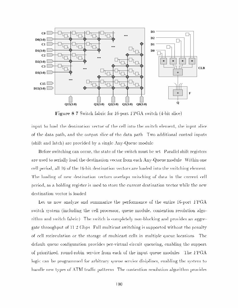
Q3(3:0) Q2(3:0) QQ1(3:0) Q0(3:0)Q15(3:0)
...
C15
D15(3:0)
C3
C2
...
D1(3:0)
CLB
F
D2(3:0)
D3(3:0)
...
...
C1
D0(3:0)
...
C0
+
**
+
**
D0
D2
D3
D1
Figure �� Switch fabric for ��port FPGA switch ���bit slice �
input to load the destination vector of the cell into the switch element� the input slice
of the data path� and the output slice of the data path� Two additional control inputs
�shift and latch are provided by a single Any�Queue module�
Before switching can occur� the state of the switch must be set� Parallel shift registers
are used to serially load the destination vector from each Any�Queue module� Within one
cell period� all � of the ��bit destination vectors are loaded into the switching element�
The loading of new destination vectors overlaps switching of data in the current cell
period� as a holding register is used to store the current destination vector while the new
destination vector is loaded�
Let us now analyze and summarize the performance of the entire ��port FPGA
switch system �including the cell processor� queue module� contention resolution algo�
rithm and switch fabric � The switch is completely non�blocking and provides an aggre�
gate throughput of ���� Gbps� Full multicast switching is supported without the penalty
of cell recirculation or the storage of multicast cells in multiple queue locations� The
default queue conguration provides per�virtual circuit queueing� enabling the support
of prioritized� round�robin service from each of the input queue modules� The FPGA
logic can be programmed for arbitrary queue service disiplines� enabling the system to
handle new types of ATM tra�c patterns� The contention resolution algorithm provides
���

fair queueing from each of the input modules� Switch�wide� prioritzed� fair queueing can
be provided with a per�port bandwidth accounting algorithm� The total latency of the
switch is ve cell periods ���� �sec � This includes the time to receive a cell from the
ber� enqueue the cell� run the contention resolution algorithm� set the switch state� and
dequeue�transmit the outgoing data�
���� Pulsar ring switch fabric
Larger switch fabrics can be built using the Pulsar�based shift register ring implemen�
tation ����� This architecture has recently resurfaced in the literature� but was renamed
the �Torus� switch ����� In such an architecture� a high speed� parallel shift register ring
is implemented that transfers the aggregate throughput of the switch through the ports�
one clock cycle at a time� The cross�sectional bandwidth of any one shift ring is nb�w�
the number of ports �n times the port rate �b � divided by the the width �w of the ring�
The architecture is well�suited for types or devices that can support a large number of
fast I�O pins� While not well�suited to FPGA technology� the requirements can be met
though the use of fast silicon or GaAs devices� Because each signal travels only a short
distance �typically shorter than � cm � I�O parasitics of the interconnect are minimal�
The logic device of a fast Pulsar ring device for use with the Any�Queue module is
shown in Figure ���� To partition the logic as per the constraints of a Vitesse H�GaAs
III gate array device implementation� the following parameters were chosen� The width
of the high speed I�O interconnect is �� bits� Each high�speed channel operates at a rate
of ��� MHz �a ��fold increase as compared to the operating frequency of the FPGA
devices � In total� there are �� high�speed inputs and �� high�speed outputs� Slower
���� MHz � TTL compatible signals are used to connect the ring device to an Any�
Queue module� These signals include the ���bit data �in and out � as well the iMCRA
control signals�
Let us partition � devices into a modular circuit board �the dashed line in Figure ��� �
A ���port switch is shown in Figure ���� A high�speed� wide connector is used along
the top and bottom of the board� For a ���port switch� these connectors are used to
���

16
32
32 32
32
16 16
Port Data Out
Port Data In
iMCRA In
iMCRA InitLatch EnableShift Enable
iMCRA Out
Ring device 0
Ring Device n+1
Ring device n-1
Ring device n+1
Ring device n
Rin
g de
vice
m+
1
Any
-Que
ue C
onne
ctor
850 Mbps Outputs
850 Mbps Inputs
Figure � Parallel shift register ring switch fabric�
Shift Register Element
Any-Queue Module
Optic I/O
(16 Devices/Board)
16 Ports
32 Port Configuration 64 Port Configuration
Master
Slave
32x1 Gbps Lower Connector
32x1 Gbps Top Connector
Front
Back
Figure �� Pulsar circuit boards�
���

interconnect front and back circuit boards �thus� �attening the ring � For larger switches�
this connector is used to extend the ring� The Any�Queue modules are attached to the
slower I�O pins to the left of the chip�
The construction of a ��port switch is also shown in Figure ���� Using the same
circuit boards as before� the ring is extended to � ports� and widened to � bits� Note
that one board acts as the master� and the other the slave� The master reads the
destination vector from the Any�Queue module in one cell cycle �� bits at a time during
each of the � subcycles of the ATM cell � As before� we can overlap the reading of new
destination vectors with switching of the previous data�
Although not necessary� the iMCRA logic can be migrated into the Pulsar ring device�
As this structure is a fast� wide� shift register ring� it is well�suited for running the
distributed iMCRA algorithm� thus allowing the contention latency to be further reduced�
For this conguration� the Any�Queue module uses the iMCRA bus to communicate
with the ring device� rather than directly among other Any�Queue modules� Destination
vectors from the Any�Queue module are shifted into the ring device via the iMCRA�in bus�
The distributed iMCRA algorithm can operate using the same ���bit data path as used
for cell transmission because only �� of the � slow clock periods are used to transfer the
ATM cell header and payload� At ��� MHz� the extra � � ������� � �� cycles of the ���
bit data path are more than su�cient for an iMCRA to support a switch with �� ports�
For each port� the master ring device solves one slice of the distributed iMCRA� and then
forwards the results to its slave�s and to the Any�Queue module via the iMCRA�out bus�
The size of the switch can be increased by mulitples of �� by extending the ring� For
each board added along the ring� an additional slave board must be added� In general�
the number of circuit boards required is ��n��� �� where n is a multiple of ��� For a
���port switch fabric� there are � circuit boards connected back to back� Additionally�
each port requires seven slave boards �eight boards in total are required to provide the
full aggregate throughput � The per�slice bandwidth of this system is ��� Gbps� Of this�
��� Gbps are used for data switching�
���

CHAPTER �
ACCOMPLISHMENTS AND FUTURE
RESEARCH
Input�bu�ered switch architectures are optimal in terms of the queue memory band�
width required for the implementation of an ATM queue module� As compared to a
shared memory or standard output bu�ered switch� an n�port input�bu�ered ATM switch
requires only ��n of the memory bandwidth� As compared to a knockout�based switch�
the n�port input�bu�ered switch requires less than a fourth of the memory bandwidth�
Further� for lower values of switch utilizations with bursty tra�c� an input�bu�ered ATM
switch using FIFO queues has a smaller cell loss than an output�bu�ered switch due to
the distributed bu�ering of cell bursts� For larger values of switch utilization� head�of�line
blocking only slightly degrades the throughput of the switch �but by less than a factor of
two � The use of per�virtual�circuit input queue can increase this throughput and provide
a better degree of per�virtual circuit quality of service�
Multicast is a critical feature of ATM networks� The recent growth of the Internet�s
Multicast Backbone �MBone has encouraged the development of ATM switches that can
e�ciently bu�er and switch multicast data�
��� Summary of Accomplishments
An input�bu�ered� multicast ATM switch has been designed and implemented for
use in the iPOINT testbed� This ��� Mbps prototype switch is fully functional and is
currently used to optically interconnect a local area network of workstations and act as
a gateway to the XUNET wide�area testbed�
The iPOINTMulticast Contention Resolution Algorithm �iMCRA has been designed
and implemented in the exiting testbed� By supporting atomic multicast� input cells from
the queue module are simultaneously delivered to all of the output ports specied by their
���

destination vectors� Only a single cell transfer from the input queue module is required
to deliver a cell to all output ports� It have been shown that the throughput of this
algorithm is near optimal�
Supporting network control hardware and software has been developed and written to
support total remote operation and programming of the iPOINT switch� Virtual circuit
establishment� switch management operations� and even hardware development can be
performed without physical access to the iPOINT testbed� Using the iPOINT switch
controller� it is possible to dynamically create and modify virtual circuits and support
switched virtual circuits� Using the switch management circuit� it is possible to monitor
cell counts and control the operational modes of the iPOINT switch� Via the FPGA
controller� it is possible to change the logic functionality of any device in the testbed�
A hardware interface to the iPOINT switch has been fully documented� Through
the use of this interface� arbitrary devices can be attached to the ATM network� An
ATM telephone has been implemented that directly transmits and receives audio and
control information between the iPOINT switch and a remote user on the ATM network�
By means of an example� it has been shown how the iPOINT hardware interface was
customized to meet the specic requirements of the ATM telephone�
Based on the existing prototype switch� the design of the enhanced� FPGA�based�
gigabit�per�second �Any�Queue� module has been presented� Through the use of the
distributed iMCRA algorithm� it is possible to support up to �� queue modules� and
thus provide an aggregate switch throughput of ��� Gbps� Further� the design of a ��
port� ���� Gbps aggregate throughput switch fabric has been documented that can be
entirely implemented using only eight FPGA devices� It is shown that this entire system
has a baseline latency of only � ATM cell periods �� �sec �
Optoelectronic devices from the CCSM have been successfully integrated into the
iPOINT testbed through the development of the � Gbps trunk port� It is shown how these
same devices can be used to interconnect the existing FPGA switch with the enhanced�
multigigabit�per�second switch�
���

��� Future Research
The implementation of the Any�Queue module is currently in progress� The design
of the circuit board is currently underway� Because the Any�Queue module uses FPGA
logic� it is possible to support rather arbitrary types of queue service disciplines� above
and beyond round�robin� prioritized� per�virtual circuit queuing� To support the trans�
port MPEG tra�c� for example� an optimal queue service discipline can dynamically
control the priority of the connection as a function of queue length and latency�
Mechanisms for �ow control and bandwidth allocation are an area for future research�
There is a great interest in providing �ow�control hardware for Available Bit Rate �ABR
tra�c� This can be implemented using the FPGA logic of the Any�Queue cell proces�
sor� At the software level� the switch controller can provide Quality of Service �QoS
guarantees by controlling bandwidth allocation and controlling queue service disciplines�
Future iPOINT research may involve the development of a wireless ATM LAN base�
station using the iPOINT hardware interface� The interface logic can be easily customized
to meet the requirements of existing wireless communication chipsets�
While the FPGA switch fabric is su�cient for an ���� Gbps switch fabric� the de�
velopment of a fast� GaAs�based shift�register ring would allow interconnection of up
to �� Any�Queue modules� While the Non�Recurring Engineering �NRE cost of such
devices has hampered development of such devices at this time� it remains an area open
for development�
��

APPENDIX A
IMCRA SIMULATOR
The iMCRA simulator predicts the throughput �number of transmitted cells forboth the iPOINT Multicast Contention Resolution Algorithm �iMCRA and for theoptimal multicast cell selection algorithm� The operation of this program is described inSection ������
A�� iMCRA C�� Source Code
�� Program� mcra�sim
�� Author� John Lockwood
�� Updated� Aug ��� ���
�� Purpose� Efficient simulation of MCRA algorithm used by iPOINT switch
include �stdlib�h
include �stdio�h
include �limits�h
include �iostream�h
include �time�h
class mcra �
private�
int size� �� Number of switch ports �maximum � sizeof�long��
double p�cell� �� Probability of a cell ready for transmission
long �matrix� �� Boolean matrix
long sw�vector� �� Winning transmission slots
long winners� �� Winning reception slots
int rx� tx� winrx� wintx� �� Statistics of solution
int verbosity�
public�
mcra �int insize� double in�cell�probability�� �� Constructor
void fill��� �� Fill with random variables
void print��� �� Display the contents of the matrix
void setverbose�� � verbosity��� ��
void setsilent�� � verbosity��� ��
void evaluate�int start�row�� �� Evaluate
void eval�optimal��� �� Evaluate optimal solution
void computestats���
���

int rxcells�� �return rx��� �� Number of input ports with � or more cells
int txcells�� �return tx��� �� Total number of cells to transmit
int win�rxcells�� �return winrx��� �� Number of input ports accepted
int win�txcells�� �return wintx��� �� Number of cells transmitted
��
mcra��mcra�int insize� double in�cell�probability� �
size � insize�
p�cell � in�cell�probability�
matrix � new long�size�� �� Bit�mapped values used for rows
winners � ��
sw�vector � ��
verbosity � �� �� Default
�
void mcra��fill�� �
int i�j�
for �i��� i�size� i��� �
matrix�i���� �� Reset values of this row
for �j��� j�size� j���
if � drand���� � p�cell �
matrix�i� �� �long� � �� j�
��
�
void mcra��evaluate�int start�row� �
sw�vector � matrix�start�row�� �� start�row always wins
int i�
winners � ���start�row�
for ��i�start�row��� � size � i��start�row� i��i��� � size�
if ���matrix�i� � sw�vector�� � �� no conflict
winners �� ���i�
sw�vector �� matrix�i��
�
�
void mcra��eval�optimal�� �
long test�vector� cur�vector�
int i�
int cur� �� Number of transmitted cells
int opt � ��� �� Optimal number of transmitted cells
�� exhaustively search for optimal input combinations
for �test�vector��� test�vector � ����size�� test�vector��� �
cur�vector � ��
���

i���
�� Verify feasibility of solution �i�e�� no conflicting cells�
for �i��� i�size� i���
if ��test�vector � ���i���� �� �matrix�i� � cur�vector�����
cur�vector �� matrix�i��
�� compute cost function
cur���
for �i��� i�size� i���
cur �� ��cur�vector � ����i������ � � � ��
�� Store solution if maximum
if �cur opt� �
winners � test�vector�
sw�vector � cur�vector�
opt � cur�
��
��
��
void mcra��computestats�� �
int i�j�
rx���
tx���
winrx���
wintx���
for �i��� i�size� i��� �
rx �� �matrix�i����� � � � ��
winrx �� ��winners � ���i���� �� matrix�i������
wintx �� ��sw�vector � ���i����� � � � ��
for �j��� j�size� j���
tx �� ��matrix�i� � ���j����� � � � ��
��
�
void mcra��print�� �
int i�j�
if �verbosity� �
cout �� Size of switch �number of ports�� �� size �� !"n!�
cout �� P�Cell arrival�� �� p�cell �� !"n!�
��
for �i��� i�size� i��� �
cout�width����
cout �� i �� � �
for �j��� j�size� j���
if �matrix�i� � ���j�
cout �� � �
���

else
cout �� � �
if �matrix�i�����
cout �� � � �� Indicate zero row
else if ��winners � ���i�����
cout �� � � �� Indicate winning row
cout �� !"n!�
��
cout �� Soln� �
for �j��� j�size� j���
if �sw�vector � ���j�
cout �� � �
else
cout �� � �
cout �� !"n!�
if �verbosity� �
cout �� TX Cells� �� wintx �� of �� tx �� !"n!�
cout �� RX Cells� �� winrx �� of �� rx �� !"n!�
cout �� !"n!�
�
�
int main�int argc� char� argv��� �
int ports�
double p�cell�
int iterations�
int i� rx��� tx��� winrx��� wintx��� winrxopt��� wintxopt���
if ���argc��# �� argc����� � �� Wrong usage�
cout �� Usage� mcra�sim number�of�ports p�cell"n �
cout �� �or� mcra�sim number�of�ports p�cell simulation�iterations"n �
return�����
��
sscanf�argv���� �d ��ports��
sscanf�argv���� �lf ��p�cell��
mcra imcra�ports�p�cell��
�� Use time as a random number seed
long tm�
time��tm��
srand���tm��
switch�argc� �
���

case #� �� Interactive Display Mode
imcra�fill���
cout �� iMCRA Algorithm"n �
imcra�evaluate����
imcra�computestats���
imcra�print���
cout �� Optimal Solution"n �
imcra�eval�optimal���
imcra�computestats���
imcra�print���
break�
case �� �� Statistical Mode
sscanf�argv�#�� �d ��iterations��
for �i��� i�iterations� i��� �
imcra�fill���
imcra�evaluate����
imcra�computestats���
rx �� imcra�rxcells�� �
tx �� imcra�txcells�� �
winrx �� imcra�win�rxcells�� �
wintx �� imcra�win�txcells�� �
imcra�eval�optimal���
imcra�computestats���
winrxopt �� imcra�win�rxcells���
wintxopt �� imcra�win�txcells���
��
cout �� ports �� � �� Number of switch ports
cout �� p�cell �� � �� P�Cell�
cout �� rx � �double� iterations �� � �� Average number of RX ports
cout �� tx � �double� iterations �� � �� Average number of TX cells
cout �� winrx � �double� iterations �� � �� Average accepted using iMCRA
cout �� wintx � �double� iterations �� � �� Average xmitted using iMCRA
cout �� winrxopt � �double� iterations �� � �� Average accepted using OPT
cout �� wintxopt � �double� iterations �� � �� Average xmitted using OPT
cout �� !"n!�
break�
��
���

return����
�
A�� iMCRA Sample Output
mcra�sim � ��
iMCRA Algorithm
Size of switch �number of ports�� �
P�Cell arrival�� ���
�� � � � � � � � � �
�� � � � � � � � � �
�� � � � � � � � � �
#� � � � � � � � � �
�� � � � � � � � �
� � � � � � � � � �
$� � � � � � � � � �
%� � � � � � � � �
Soln� � � � � � � � �
TX Cells� $ of ��
RX Cells� � of $
Optimal Solution
Size of switch �number of ports�� �
P�Cell arrival�� ���
�� � � � � � � � � �
�� � � � � � � � � �
�� � � � � � � � � �
#� � � � � � � � �
�� � � � � � � � �
� � � � � � � � � �
$� � � � � � � � � �
%� � � � � � � � � �
Soln� � � � � � � � �
TX Cells� % of ��
RX Cells� � of $
���

APPENDIX B
ATM CELLLEVEL TESTING PROGRAM
The both program runs on a network�attached workstation� The program generatesATM cells with variable�length bursts� receives the cells after they loop through theswitch� then calculates the percentages of corrupted and missing cells� The operation ofthis program is described in Section ������
��
� Program� both�c
� Directory� �ipoint��ATM�hwtest
� Purpose� Cell�level ATM testing of the iPOINT Switch Hardware
� Rqrd hardware� SBA����
� Author� John Lockwood
��
include �stdio�h
include �strings�h
include �ctype�h
include atm�struct�h
include atm�lib�h
long TXcell���� � �
�x��������
�x���������
�x���������
�x���������
�x���������
�xFF����$�
�x�%�����A�
�x�B�C�D�E�
�x�F����
�x#�$�
�x%��A�
�x#�#�#�##�
�x#�##$#%�
�x#�#�����
��
long correctcell���� � �
�x��������
���

�xE��������
�x���������
�x���������
�x���������
�xFF����$�
�x�%�����A�
�x�B�C�D�E�
�x�F����
�x#�$�
�x%��A�
�x#�#�#�##�
�x#�##$#%�
�x#�#�����
��
main�� �
int i�
int j���
int itctr�
int blastsize�����
int iterations�����
int cells�received�
int receive�delay������ �� usec ��
int iteration�delay�������� �� usec ��
int error�count�
int cell�in�error�
int verbose���
int nothing�
int check�header���
long mycell�����
struct atm�device �atm�dev�
if � init�atm�ATM�DEVICE�NAME� �atm�dev� �� �� � �
fprintf�stderr� Couldn!t get ATM device�"n ��
exit����
�
for �itctr��� itctr�iterations� itctr�� � �
�� TX Cells ��
for �i��� i�blastsize� i��� �
send�raw�atm�dev� TXcell��
for �j��� j�itctr� j���
nothing��j�
���

��
usleep�receive�delay��
�� RX Cells ��
cells�received���
cell�in�error���
error�count���
for �j��� j�blastsize���� j��� �
if � CellsReady�atm�dev� � �
cell�in�error���
cells�received���
recv�raw�atm�dev�mycell��
if �check�header�
if ��mycell��� �� correctcell���� ��
��mycell��� � �xFF��FFFF� �� �correctcell��� � �xFF��FFFF��� �
cell�in�error���
if �verbose�
printf� ERROR in header� �x���lX received� ���lX expected"n �
mycell����correctcell�����
��
for �i��� i���� i���
if �mycell�i���correctcell�i�� �
cell�in�error���
if �verbose�
printf� ERROR� Word �d was �x���lX� expected �x���lX"n �
i�mycell�i��correctcell�i���
��
if ��mycell��#� � �xFFFF����� �� �correctcell��#� � �xFFFF������ �
cell�in�error���
if �verbose�
printf� ERROR in trailer� �x���lX received� �x���lX expected"n �
mycell��#��correctcell��#���
��
error�count��cell�in�error�
��
��
printf� �����������������������������������������"n ��
���

printf� Cell Spacing �A�U��� �d"n �itctr��
printf� Cells Transmitted� �d"n �blastsize��
if �error�count�
printf� � Cells with ERRORS� �d"n �error�count��
if �blastsize�cells�received�
printf� � MISSING Cells� �d"n �blastsize�cells�received��
printf� Good Cells Received� �d �����lf���"n �
cells�received�error�count�
� ����� � �cells�received � error�count �� � �double� blastsize ��
printf� �����������������������������������������"n ��
fflush�stdout��
usleep�iteration�delay��
�
�
��

APPENDIX C
IPOINT SWITCH SCHEMATICS
The schematics of this appendix combined with the VHDL code of Appendix Ddocument the design of the iPOINT switch� The relationship between these hierarchicalcomponents and the operation of the individual elements are discussed in Section ��� andillustrated in Figure ���� Electronic versions of these les �Postscript� EDIF� XNF areavailable from the author via email to lockwood�ipoint�vlsi�uiuc�edu�
���

Figure C�� Top level switch �sw��ttm �
���

Figure C�� Switch management unit �management �
Figure C�� Timing control �timingctrl �
���

Figure C�� Rom cell �romcell �
���

Figure C�� Microprocessor interface �uproc �
���

Figure C�� Master switch �masterswitch �
���

Figure C�� Switching element �FPGASwitch �
���

Figure C� Switching primitive ���switch �
Figure C�� Logical trunk port control �portT �
���

Figure C��� Physical trunk port I�O �trunkport �
���
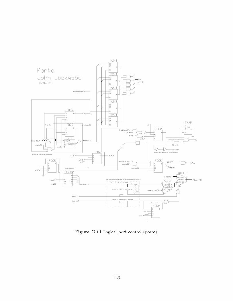
Figure C��� Logical port control �portc �
��

Figure C��� Physical port I�O �portPB �
Figure C��� Physical port I�O �portPL �
���

Figure C��� Physical port I�O �portPR �
Figure C��� Physical port I�O �portPT �
���

APPENDIX D
IMCRA IMPLEMENTATION
The iMCRA of the iPOINT switch determines which cells are to be transmittedfrom the input queue modules� The VHDL implementation of this component supportsatomic multicast and round�robin fair queueing� The iMCRA component appears inthe masterswitch component of Figure C�� The operation of the iMCRA algorithm isdescribed in Section �����
D�� iMCRA� VHDL Entity
������������������������������������������������������������
�� iMCRA� iPOINT Multicast Contention Resolution Algorithm
�� Written By� John Lockwood for iPOINT Project
�� Updated� ������
������������������������������������������������������������
�� This program is used to select the cells for
�� transmission
������������������������������������������������������������
�� Inputs�
�� REQ� Request vectors for each input port
�� START� Begin CRA Algorithm �first cycle�
�� PRIORITY� Cell Priority
�� RRSHIFT� Shift Round�Robin Priority Selection
�� RST� Power�on reset
�� Outputs�
�� SEL� Selected Vector
�� ACCEPT� Cell Accepted for transmission
�� FINISH� Finish CRA Algorithm �last cycle�
�� RR� Round�robin vector
������������������������������������������������������������
LIBRARY MGC�PORTABLE�
USE MGC�PORTABLE�QSIM�LOGIC�ALL�
USE MGC�PORTABLE�QSIM�RELATIONS�ALL�
ENTITY imcra IS
PORT �
REQ� � IN qsim�state�vector�% DOWNTO ���
REQ� � IN qsim�state�vector�% DOWNTO ���
���

REQ� � IN qsim�state�vector�% DOWNTO ���
REQ# � IN qsim�state�vector�% DOWNTO ���
REQ� � IN qsim�state�vector�% DOWNTO ���
REQ � IN qsim�state�vector�% DOWNTO ���
REQ$ � IN qsim�state�vector�% DOWNTO ���
REQ% � IN qsim�state�vector�% DOWNTO ���
clk � IN qsim�state�
start � IN qsim�state�
finish � OUT qsim�state�
rrshift � IN qsim�state�
rst � IN qsim�state�
PRIORITY � IN qsim�state�vector�% DOWNTO ���
SEL� � OUT qsim�state�vector�% DOWNTO ���
SEL� � OUT qsim�state�vector�% DOWNTO ���
SEL� � OUT qsim�state�vector�% DOWNTO ���
SEL# � OUT qsim�state�vector�% DOWNTO ���
SEL� � OUT qsim�state�vector�% DOWNTO ���
SEL � OUT qsim�state�vector�% DOWNTO ���
SEL$ � OUT qsim�state�vector�% DOWNTO ���
SEL% � OUT qsim�state�vector�% DOWNTO ���
ACCEPT� � OUT qsim�state�
ACCEPT� � OUT qsim�state�
ACCEPT� � OUT qsim�state�
ACCEPT# � OUT qsim�state�
ACCEPT� � OUT qsim�state�
ACCEPT � OUT qsim�state�
ACCEPT$ � OUT qsim�state�
ACCEPT% � OUT qsim�state�
RR � OUT qsim�state�vector�% DOWNTO ��
��
END imcra�
���

D�� iMCRA� VHDL Architecture
������������������������������������������������������������
�� iMCRA� iPOINT Multicast Contention Resolution Algorithm
�� Written By� John Lockwood for iPOINT Project
�� Updated� ������
������������������������������������������������������������
ARCHITECTURE behav of imcra IS
SIGNAL cntreg � qsim�state�vector�% DOWNTO ���
SIGNAL port� � qsim�state�vector�% DOWNTO ���
SIGNAL port� � qsim�state�vector�% DOWNTO ���
SIGNAL port� � qsim�state�vector�% DOWNTO ���
SIGNAL port# � qsim�state�vector�% DOWNTO ���
SIGNAL port� � qsim�state�vector�% DOWNTO ���
SIGNAL port � qsim�state�vector�% DOWNTO ���
SIGNAL port$ � qsim�state�vector�% DOWNTO ���
SIGNAL port% � qsim�state�vector�% DOWNTO ���
SIGNAL accept � qsim�state�vector�% DOWNTO ���
SIGNAL cycle�cnt � qsim�state�vector�# DOWNTO ���
�� Contention Resolution Stage
PROCEDURE CRA�Stage �
SIGNAL prev�port � IN qsim�state�vector�% DOWNTO ���
SIGNAL nport � OUT qsim�state�vector�% DOWNTO ���
SIGNAL req � IN qsim�state�vector�% DOWNTO ���
SIGNAL cnt � IN qsim�state�
SIGNAL accept � OUT qsim�state � IS
BEGIN
IF �cnt�!�!� THEN
accept �� !�!� �� Always accept first cell
nport �� req� �� Full set� less request vector
ELSIF ��prev�port AND req�� �������� � THEN
accept �� !�!� �� Accept non�conflicting cell
nport �� prev�port OR req� �� Pass along remaining vector
ELSE
accept �� !�!� �� Reject cell
nport �� prev�port� �� Pass along orignal vector
END IF�
END CRA�Stage�
���

�� Criteria for determining whether or not a cell was selected
FUNCTION CRA�Accept �
accept � qsim�state�
req � qsim�state�vector�% DOWNTO �� �
RETURN qsim�state�vector IS
BEGIN
IF �accept�!�!� THEN
RETURN req� �� Accepted Cells switched
ELSE
RETURN �������� � �� Rejected Cell buffered
END IF�
END CRA�Accept�
BEGIN
�� Round�robin� per�port� fair queuing
Fair�Queue� PROCESS�clk�
BEGIN
IF�clk!EVENT AND clk�!�! AND clk!LAST�VALUE�!�!� THEN
IF�rst�!�!� THEN
cntreg �� �������� �
ELSIF�rrshift�!�!� THEN
cntreg �� cntreg��� � cntreg�% DOWNTO ���
END IF�
END IF�
END PROCESS Fair�Queue�
�� Run distributed CRA Algorithm on each port
CRA�Solve� PROCESS�clk�
BEGIN
IF�clk!EVENT AND clk�!�! AND clk!LAST�VALUE�!�!� THEN
CRA�Stage�port%�port��req��cntreg����accept�����
CRA�Stage�port��port��req��cntreg����accept�����
CRA�Stage�port��port��req��cntreg����accept�����
CRA�Stage�port��port#�req#�cntreg�#��accept�#���
CRA�Stage�port#�port��req��cntreg����accept�����
CRA�Stage�port��port�req�cntreg���accept����
CRA�Stage�port�port$�req$�cntreg�$��accept�$���
CRA�Stage�port$�port%�req%�cntreg�%��accept�%���
END IF�
END PROCESS CRA�Solve�
�� Algorithm�Dependent� Running time of CRA
���

Cycle�Count� PROCESS�clk�
BEGIN
IF �clk!EVENT AND clk�!�! and clk!LAST�VALUE�!�!� THEN
IF �start�!�!� THEN
cycle�cnt �� ���� �
ELSIF �cycle�cnt �� ���� � THEN
cycle�cnt �� cycle�cnt � � �
END IF�
END IF�
END PROCESS Cycle�Count�
�� Set flag to indicate completion of algorithm
Finish�Flag� PROCESS�cycle�cnt�
BEGIN
IF �cycle�cnt � ���� � THEN
finish �� !�!�
ELSE
finish �� !�!�
END IF�
END PROCESS Finish�Flag�
�� Display current value of round�robin pointer
RR �� cntreg�
�� Selected outgoing ports for accepted cells
sel� �� CRA�Accept�accept����req���
sel� �� CRA�Accept�accept����req���
sel� �� CRA�Accept�accept����req���
sel# �� CRA�Accept�accept�#��req#��
sel� �� CRA�Accept�accept����req���
sel �� CRA�Accept�accept���req��
sel$ �� CRA�Accept�accept�$��req$��
sel% �� CRA�Accept�accept�%��req%��
�� Accepted input cells
accept� �� accept����
accept� �� accept����
accept� �� accept����
accept# �� accept�#��
accept� �� accept����
accept �� accept���
accept$ �� accept�$��
accept% �� accept�%��
END behav�
���

APPENDIX E
VPIVCI SWITCH CONTROLLER
The vpivci program allows a user to create and modify virtual circuits on the iPOINTswitch� The operation of this program is described in Section ������
�� Program� vpivci�c
� Author� John Lockwood
� Purpose� Transfer translation commands to iPOINT switch
� Parameters�
� out�vci �����$� bits � VCI����� � #���� �
� out�vpi ����#� # bits � VPI����VPI����� � �������%��$�#������ �
� notused ������� � bit
� Priority ������� � bits ����highest�
� Destintation � �� � bits
� Address � �� �� bits � VPI����VCI�#��� VPI���$����VCI�����
� Note� Transmit high bit first� ��� bits total�
� Example�
� Incoming Cell� VPI��$�VCI��
� Destination Vector� �����b �broadcast�
� Outgoing Cell� VPI���VCI�%
� � Binary word� ����������x����������������
� Transmission Algorithm�
� AND ��������������������������� �bin�� shift �� � repeat
� �On last bit� DONE will be high �and clocked with Data����
��
include �stdio�h
include �fcntl�h
include �termios�h
include �string�h
include �unistd�h
include �sys�mman�h
include �linux�mm�h
define DEBUG�x�
define DEBUGS�x�
static void inline port�out�char value� unsigned short port� �
��asm�� volatile � outb �����
�� a ��char� value�� d ��unsigned short� port���
�
���

static unsigned char inline port�in�unsigned short port� �
unsigned char �v�
��asm�� volatile � inb �����
� �a ��v�� d ��unsigned short� port���
return �v�
�
define PORTA �x#�
define PORTB �x#�
define PORTC �x#�
define PORTCONTROL �x##
define MODEAoutBoutCin �x��
�� Electrical connections
� A���� Data TX
� A���� Clk TX
� A���� Done � �PT�
� A�#�� Done � �PR�
� A���� Done � �PL�
� A��� Done # �PB�
� A�$�� Done Switch
� A�%�� Done Trunk
� C���� SW Req
� C���� SW Data RX
��
define DATA�TX �unsigned char� �x�
define DATA�CLK �unsigned char� �x�
define DONE� �unsigned char� �x�
define SWREADY �unsigned char� �x�
define SWDATA�RX �unsigned char� �x�
�� Waveforms� data changes on neg� edge
� clk� ���������������������� �� �������� ��
� data� ���������������������� �� �������� ��
� done� ���������������������������������� ��
��
void transmit�unsigned int data�unsigned char portnum� �
�� Send �� bits� MSB first ��
int i�
for �i���� i �� i��� �
DEBUGS�usleep�������
���

if � �data i� � �unsigned int� �x���� � �
port�out�DATA�TX� PORTA��
DEBUGS�usleep�������
port�out��DATA�TX � DATA�CLK�� PORTA��
DEBUG� printf� � �� fflush�stdout�� �
�
else �
port�out��x��� PORTA��
DEBUGS�usleep�������
port�out�DATA�CLK� PORTA��
DEBUG� printf� � �� fflush�stdout�� �
�
��
DEBUGS� usleep������ �
if � data � �unsigned int� �x���� � �
port�out�DATA�TX � �DONE� �� portnum�� PORTA��
DEBUGS� usleep������ �
port�out�DATA�TX � �DONE� �� portnum� � DATA�CLK� PORTA��
DEBUG� printf� � �� fflush�stdout�� �
�
else �
port�out� �DONE� �� portnum�� PORTA��
DEBUGS� usleep�������
port�out� �DONE� �� portnum� � DATA�CLK� PORTA��
DEBUG� printf� � �� fflush�stdout�� �
��
port�out� �unsigned char� �x��� PORTA��
��
�� global variables ��
unsigned int in�port� in�vpi� in�vci� dest� pri� out�vpi� out�vci� addr�
unsigned int vpi�map� dta�
int createvpivci�� �
printf� Create new translation for port� �d"n �in�port��
printf� Incoming VPI�VCI��d��d"n �in�vpi�in�vci��
printf� Destination Vector� �x �hex�� Priority� �d"n �dest�pri��
printf� Outgoing VPI�VCI��d��d"n �out�vpi�out�vci��
addr���in�vpi � �unsigned int� �x��� � �in�vci � �unsigned int� �xF���
printf� Address� �x �hex�"n �addr��
if �in�port � � printf� Error� in�port � �����"n �� return���� ��
if �pri #� �printf� Error� Priority � ����#�"n �� return���� ��
��

if �out�vci #�� � printf� Error� out�vci � ����#��"n �� return���� ��
if ��out�vpi # �� out�vpi��$� �� �out�vpi ���� �
printf� Error� out�vpi � ��������%��$�#�������"n �� return���� ��
if �in�vci �� � printf� Error� in�vci � ������"n �� return���� ��
if �in�vpi���$ �� in�vpi���� �
printf� Error� in�vpi���$���"n �� return���� ��
vpi�map � ��out�vpi � �x��� �� � �out�vpi � �x#��
dta�addr � dest�� � pri���� � vpi�map���# � out�vci���$�
printf� Transmitting �leftmost bit first�� ��
transmit�dta�in�port��
printf� "n ��
printf� VPI�VCI Translation created�"n ��
return����
��
void setswitch�� � transmit� �unsigned int� �x�FFFFF� ��� ��
void setfastswitch�� � transmit� �unsigned int� �x���FFF� ��� ��
void clearswitch�� � transmit� �unsigned int� �x������� ��� ��
void setaudio�int dest� � transmit��unsigned int� ��xF � dest�� ��� ��
void main�argc�argv�
int argc�
char� argv���
�
FILE� vlist�
int d�
if �strcmp� vpivci �argv������� �� argc ��� �� argc��� �� argc��# ��
strcmp� audio �argv������� �� argc ��� � �
printf� Usage� vpivci in�port in�vpi in�vci destvector pri out�vpi out�vci"n ��
printf� �or� vpivci filename"n ��
printf� �or� audio �dest� "n ��
exit�����
�
if �ioperm��x#��������ioperm��x#��������ioperm��x#��������
ioperm��x##������ �
printf� can!t get I�O permissions for PC� Run this program as root"n ��
exit�����
���

�
printf� Running� �s"n �argv�����
port�out�MODEAoutBoutCin�PORTCONTROL��
�� ATM�telephone transmit destination ��
if �strcmp� audio �argv�������� �
d�strtol�argv�����char ��� NULL� �$��
printf� Audio Dest��x"n �d�� setaudio�d��
exit����
�
�� VPIVCI Command�line mode ��
if �argc���� �
sscanf�argv���� �ud ��in�port��
sscanf�argv���� �ud ��in�vpi��
sscanf�argv�#�� �ud ��in�vci��
sscanf�argv���� �ud ��dest��
sscanf�argv��� �ud ��pri��
sscanf�argv�$�� �ud ��out�vpi��
sscanf�argv�%�� �ud ��out�vci��
createvpivci���
exit����
�
�� VPIVCI File�line mode ��
if �argc���� �
if ��vlist�fopen�argv���� r ����NULL� �
printf� Error� Could not open file� �s"n �argv�����
exit�����
�
while�fscanf�vlist� �u �u �u �u �u �u �u"n �
�in�port� �in�vpi� �in�vci� �dest� �pri� �out�vpi� �out�vci���EOF�
createvpivci���
fclose�vlist��
exit����
��
�
���

APPENDIX F
FPGA CONTROLLER
The r�tcp client program allows a remote user to select the FPGA device that isto be reprogrammed� The s�tcp server awaits commands from the r�tcp client andcontrols the FPGA demultiplexor hardware� TCP�IP sockets are used to transfer controlinformation between the client and server� The operation of the FPGA controller isdescribed in Section ����
F�� Include File
include �errno�h
include �sys�types�h
include �sys�socket�h
include �fcntl�h
include �netinet�in�h
include �netdb�h
include �stdio�h
include �unistd�h
define DEBUG�x� x
define TRUE �
define FALSE �
define BUFLEN ���$
define PORT ��%
F�� S�TCP Program
��
� Program� S�TCP� Server for iPOINT FPGA Controller
� Author� John lockwood
� Notes� This program runs as a daemon process on
� the iPOINT switch controller �fermion�vlsi�uiuc�edu�
� Directory� fermion�&lockwood�s�tcp
���

� Usage� s�tcp
� Privileges� Must be run as root �writes to hardware�
��
include s�tcp�h
include �termios�h
include �string�h
include �sys�mman�h
include �linux�mm�h
define DEBUGS�x�
define PORTA �x#�
define PORTB �x#�
define PORTC �x#�
define PORTCONTROL �x##
define MODEAoutBoutCin �x��
��
� B���� FPGA��
� B���� FPGA��
� B���� FPGA��
��
static void inline port�out�char value� unsigned short port� �
��asm�� volatile � outb �����
�� a ��char� value�� d ��unsigned short� port���
�
static unsigned char inline port�in�unsigned short port� �
unsigned char �v�
��asm�� volatile � inb �����
� �a ��v�� d ��unsigned short� port���
return �v�
�
int ibuffer� �� input buffer ��
int ival� �� input value ��
int msgsock� sock�
main �argc� argv�
int argc�
char ��argv�
�
int length�
���

struct sockaddr�in server�
int rval� rval��
if �ioperm��x#��������ioperm��x#��������ioperm��x#��������
ioperm��x##������ �
printf� can!t get I�O permissions for PC� Run this program as root"n ��
exit�����
�
port�out�MODEAoutBoutCin�PORTCONTROL��
sock � socket �AF�INET� SOCK�STREAM� ���
if �sock � �� � perror � opening stream �� exit ����� �
server�sin�family � AF�INET�
server�sin�addr�s�addr � INADDR�ANY�
server�sin�port � htons �PORT��
DEBUG� printf� bind��"n �� �
if �bind �sock� �struct sockaddr �� �server� sizeof �server���
� perror � binding �� exit����� �
length � sizeof �server��
DEBUG� printf� Socket Port� �d"n �ntohs�server�sin�port��� �
DEBUG� printf� listen��"n �� �
listen �sock� ��
while �TRUE�
�
DEBUG� printf� accept��"n �� �
msgsock � accept �sock� �� ���
if �msgsock��� � perror� accept error� �� exit����� ��
DEBUG� printf� recv�� "n �� �
if ��rval � recv �msgsock� �char�� �ibuffer� sizeof�ibuffer�� ��� � ��
� perror � reading msg �� close �msgsock�� exit����� �
�� Convert to data type for this machine ��
ival � ntohl �ibuffer��
�� Action ��
printf� Port �d �ival��
port�out� �unsigned char� ival� PORTB��
�� send value back ��
if �rval� � send�msgsock� �char�� �ibuffer� sizeof�ibuffer�� �� � ��
���

� perror � error sending msg �� close �msgsock�� exit����� ��
��
�
F�� R�TCP Program
��
� Program� R�TCP� Client for iPOINT FPGA Controller
� Author� John lockwood
� Notes� This program runs from any machine� and allows
� selecting the FPGA device to be downloaded
� Directory� fermion�&lockwood�s�tcp
� Usage� r�tcp host device
� host� fermion�vlsi�uiuc�edu
� device� ���%
��
include s�tcp�h
main �argc� argv�
int argc�
char ��argv�
�
int sock� len� ival� ibuffer� rbuffer� rval�
struct sockaddr�in server�
struct hostent �hp�
bzero� �char �� �server� sizeof�server� ��
server�sin�family � AF�INET�
server�sin�port � htons �PORT��
DEBUG� printf� socket"n �� �
sock � socket �AF�INET� SOCK�STREAM� ���
if �sock � �� � perror � opening socket �� exit ����� �
DEBUG� printf� gethostbyname� �s"n �argv����� �
if ��hp � gethostbyname �argv�������NULL�
� perror� herror� gethostbyname �� exit����� �
DEBUG� printf� h�name��s"n �hp� h�name�� �
DEBUG� printf� h�length��d"n �hp� h�length�� �
���

DEBUG� printf� memcpy"n �� �
memcpy ��char �� �server�sin�addr� �char �� hp� h�addr� hp� h�length��
DEBUG� printf� inet�ntoa��s"n �inet�ntoa�� ��struct in�addr �� �hp� h�addr� ���� �
DEBUG� printf� connect"n �� �
if �connect �sock� �struct sockaddr �� �server� sizeof �server�� � ��
� close �sock�� perror � conn sock failed� �� exit ���� �
ival � atoi�argv�����
ibuffer � htonl�ival��
if �send �sock� �char�� �ibuffer� sizeof�ibuffer�� �� � ��
perror � writing ��
len � read�sock� �char�� �rbuffer� sizeof�rbuffer���
rval � ntohl�rbuffer��
printf� Transmitted� �d �rval��
close �sock��
�
���

APPENDIX G
ATM TELEPHONE
The ATM telephone is a hardware unit that directly attaches to the iPOINT switch�By transmitting voice samples and control information within ATM cells� the ATM tele�phone allows a user to call and speak with other users connected to the ATM network�To simplify the construction of the ATM telephone hardware� the interface logic of theiPOINT switch FPGA was modied to perform cell assembly� header generation� andheader removal� The port I�O interface of Figure C��� was replaced with the logic ofFigure G�� and the control logic of Figure C��� was replaced with the logic of Figure G���In addition to building the hardware� UNIX application software was written that allowsthe ATM telephone to call users on a multimedia�equipped� network�attached worksta�tion� The source code for this program is given in Section G��� The operation of theATM telephone is described in Section ���
G�� FPGA Circuit Modi�cation
Figure G�� ATM telephone port I�O �portPBp
���

Figure G�� ATM telephone port control �portaudio �
���

G�� Multimedia Workstation Application Software
��
� program� atm�phone�c
� directory� �ipoint��ATM�phone
� purpose� Workstation interface to iPOINT hardware telephone
� Reqrd hardware� Sun SS�� with �$�bit audio �or better�� SBA����
� Note� ATM�DEVICE�NAME must be defined as �dev�sbus�� etc��
� author� John Lockwood
��
include �stdio�h
include �strings�h
include �ctype�h
include atm�struct�h
include atm�lib�h
include �sys�socket�h
include �sys�ioctl�h
include �sun�audioio�h
define IDLEMAX ���
main�� �
int i�j�k�
�� ATM Variables ��
struct atm�device �atm�dev�
long TXcell�����
long RXcell�����
char �TXbuf � �char�� TXcell � $� �� An array of �� bytes �part of TXcell� ��
char �RXbuf � �char�� RXcell � $�
char t�buf�������
char r�buf�������
�� Audio Variables ��
static int audiofd�
static audio�info�t au�info�
int bytes�read�
int idlecnt��int� IDLEMAX�
�� File Variables ��
int ringfd�
static char �phonelist���
� ����$ � #��$$%� � ##�#��� � ����%% � #������ � �%$$�$� ��
��

static char �names���
� john � arpeet � A�P� � kang � chris � big ��
int dirsize�$�
int found���
char tempbuf�����
�� Key Mappings ��
static char convcode�� � ��#�$%���� �
�� Open Audio Device ��
if ��audiofd � open� �dev�audio � O�RDWR�� �� ��
printf� ��� WARNING� Can!t open audio device ���"n ��
�� get info ��
ioctl�audiofd� AUDIO�GETINFO� �au�info��
�� set options ��
au�info�record�sample�rate � �����
au�info�record�channels � ��
au�info�record�encoding � AUDIO�ENCODING�LINEAR�
au�info�record�precision � �$�
au�info�record�port � AUDIO�MICROPHONE�
au�info�record�gain � #�� �� guess ��
au�info�play�sample�rate � �����
au�info�play�channels � ��
au�info�play�precision � �$�
�� au�info�play�port � AUDIO�SPEAKER� ��
au�info�play�port � AUDIO�HEADPHONE�
au�info�play�encoding � AUDIO�ENCODING�LINEAR�
�� write options ��
ioctl�audiofd� AUDIO�SETINFO� �au�info��
�� Open ATM Device ��
if � init�atm�ATM�DEVICE�NAME� �atm�dev� �� �� � �
fprintf�stderr� Couldn!t get ATM device�"n ��
exit����
�
TXcell� ����x�������� �� Use VPI��� VCI�� Flags�� �always send this� ��
TXcell� ����x��������� �� Generate Header CRC ��
TXcell��#���x#�#������ �� Trailing Flags ��
while��� �
if �idlecnt�IDLEMAX� idlecnt���
�� Receive and print all cells ��
while � CellsReady�atm�dev� � �
���
idlecnt���
�� �� Incoming Data �� ��
recv�raw�atm�dev�RXcell��
�� �� Process control cells �� ��
if ��RXcell�����x������F�����x%�� �
printf� Ring� Ring� Number dialed� ��
for �i��� i�%� i��� �
RXbuf�i��convcode�RXbuf�i���x�F��
putchar�RXbuf�i���
��
printf� "n ��
�� �� Search phone book for matching number �� ��
�� �� Every user can choose a ''distinctive ring!! ��
found���
for �i��� i�dirsize� i��� �
if �strncmp�RXbuf�phonelist�i��%����� �
printf� Phone call for �s"n � names�i���
strcpy�tempbuf�names�i���
found���
�
��
�� �� Generic sound of ringing telephone �� ��
if �found���� strcpy�tempbuf� ring�$�dat ��
if ��ringfd�open�tempbuf� rb �����
printf� error� could not open �s"n �tempbuf��
else �
printf� Reading file� �s"n � tempbuf��
au�info�play�port � AUDIO�SPEAKER�
ioctl�audiofd� AUDIO�SETINFO� �au�info��
while�read�ringfd� RXbuf� ��� ��
write�audiofd�RXbuf�����
close�ringfd��
sleep�#��
au�info�play�port � AUDIO�HEADPHONE�
ioctl�audiofd� AUDIO�SETINFO� �au�info��
�� flush out cells ��
while � CellsReady�atm�dev� �
recv�raw�atm�dev�RXcell��
��
���

�
else �
�� �� Audio Cell �� ��
for �i��� i���� i��� �
r�buf���i���unsigned char� �x�� ( �unsigned char� RXbuf�i��
r�buf���i������
��
write�audiofd�r�buf�������
��
��
�� �� Microphone� FIber �� ��
�� Fill Transmit Buffer with Data ��
bytes�read � read�audiofd�t�buf�������
�� Transmit the Cell ��
for �i��� i���� i���
TXbuf�i��t�buf���i��
if �idlecnt�IDLEMAX�
send�raw�atm�dev� TXcell��
��
�
���

REFERENCES
��� J� B� Lyles and D� C� Swinehart� �The emerging gigabit environment and the roleof local ATM�� IEEE Communications� pp� ��%��� Apr� �����
��� R� H&andel and M� N� Huber� Integrated Broadband Networks� An Introduction toATM�Based Networks� Reading� Massachusetts� Addison�Wesley� �����
��� D� J� Blumenthal� K� Y� Chen� J� Ma� R� J� Feuerstein� and J� R� Sauer� �Demon�stration of a de�ection routing ��� photonic switch for computer interconnnects��IEEE Photonics Technology Letters� vol� �� pp� ��%���� Feb� �����
��� T� Kozaki� Y� Sakurai� O� Matsubara� M� Mizukami� M� Uchida� Y� Sato� andK� Asano� ��� x �� shared bu�er type ATM switch VLSIs for B�ISDN�� in ICC���� pp� ���%���� IEEE� �����
��� Y� Yeh� M� G� Hluchyj� and A� S� Acampora� �The Knockout switch� A simple� mod�ular architecture for high%performance packet switching�� IEEE Journal on SelectedAreas in Communications� vol� SAC��� pp� ����%����� Oct� �����
�� S� C� Liew� �Performance of input�bu�ered and output�bu�ered ATM switches underbursty tra�c� Simulation study�� in Globecom ���� vol� �� pp� ����%����� �����
��� A� G� Fraser� C� R� Kalmanek� A� E� Kaplan� W� T� Marshall� and R� C� Restrick��Xunet �� A nationwide testbed in high%speed networking�� in INFOCOM� pp� ���%���� �����
��� C� R� Kalmanek� S� P� Morgan� and R� C� Restrick� III� �A high�performance queue�ing engine for ATM networks�� in International Switching Symposium ��� Oct������
��� T� T� Lee� �Nonblocking copy networks for multicast packet switching�� IEEE Jour�nal on Selected Areas in Communications� vol� � pp� ����%���� Dec� �����
���� Y� Baozong� �Performance analysis of internal bu�ered crossbar�based ATM switcheswith LQFS policy�� in TENCON� pp� ���%���� �����
���� I� Widjaja and A� Leon�Garcia� �The helical switch� A multipath ATM switch whichpreserves cell sequence�� in INFOCOM� pp� ����%����� �����
���� H� S� Kim� �Design and performance of multinet switch� A multicast ATM switcharchitecture with partially shared bu�ers�� IEEEACM Transactions on Networking�vol� �� pp� ���%���� Dec� �����
���� H� S� Kim� �Multinet switch� Multistage ATM switch architecture with partiallyshared bu�ers�� in INFOCOM� pp� ���%���� �����
���

���� G� J� Murakami� �Non�blocking packet switching with shift�register rings�� PhDdissertation� University of Illinois at Urbana%Champaign� �����
���� H� Duan� J� W� Lockwood� and S� M� Kang� �Full parallel cell scheduling of inputqueueing structures for scalable ultra�broadband optoelectronic ATM switching�� inPhotonics East� �Philadelphia� PA � Oct� �����
��� T� H� Corman� C� E� Leiserson� and R� L� Rivest� Introduction to Algorithms� Cam�bridge� MA� MIT Press� �����
���� T� V� Lakshman� A� Bagchi� and K� Rastani� �A graph�coloring scheme for schedul�ing cell transmissions and its photonic implementation�� IEEE Transactions onCommunications� vol� ��� pp� ���%����� Feb��Mar��Apr� �����
���� Fore Systems� Inc�� SBA���� SBus ATM Computer Interface User�s Manual� version��� ed�� �����
���� AMD� TAXIchip Integrated Circuits� rev� ��� ed�� �����
���� J� W� Lockwood� C� Cheong� S� Ho� B� Cox� S� M� Kang� S� G� Bishop� and R� H�Campbell� �The iPOINT testbed for optoelectronic ATM networking�� in Conferenceon Lasers and Electro�Optics� �Baltimore� MD � pp� ���%���� �����
���� B� Cox� �A STREAMS device driver for the fore SBA������ Available via In�ternet anonymous ftp from ipoint�vlsi�uiuc�edu as �pub�ipoint�Documents��device�driver�ps� Apr� �����
���� J� W� Lockwood� �The ipoint testbed for optoelectronic atm networking�� Tech�Rep�� UIUC�BI�VLSI������� Beckman Institute� �����
���� H� Duan� J� W� Lockwood� and S� M� Kang� �FPGA prototype queueing modulefor high performance ATM switching�� in Proceedings of the Seventh Annual IEEEInternational ASIC Conference� �Rochester� NY � pp� ���%���� Sept� �����
���� J� W� Lockwood� H� Duan� J� J� Morikuni� S� M� Kang� S� Akkineni� and R� H�Campbell� �Scalable optoelectronic ATM networks� The iPOINT fully functionaltestbed�� IEEE Journal of Lightwave Technology� pp� ����%����� June �����
���� J� W� Lockwood� �iPOINT gigabit OEIC specications�� Available via Inter�net anonymous ftp from ipoint�vlsi�uiuc�edu as �pub�ipoint�Documents�
�specs�ps� Mar� �����
��� J� W� Lockwood� �Low frequency requirements for �B���B encoded data�� Avail�able via Internet anonymous ftp from ipoint�vlsi�uiuc�edu as �pub�ipoint�
�Documents�specs�lf�ps� Nov� �����
���

���� S��M� Tan and R� H� Campbell� �x�ATM� A portable atm protocol toolkit�� Availablevia WWW at http���choices�cs�uiuc�edu�latex�docs�suite�suite�html������
���� M� Makkar� �Hardware language synthesis for ATM switch management unit intoXilinx FPGAs�� in Undergraduate Summer Reports� UIUC Center for CompoundSemiconductor Microelectronics� �����
���� A� Patel and A� Singh� �ATM phone�� in ECE� � Senior Design Projects� UIUCDepartment of Electrical and Computer Engineering� �����
���� H� Schulzrinne� �Voice communication across the internet� A network voice termi�nal�� Anonymous ftp from gaia�cs�umass�edu as �pub�nevot�nevot�ps�Z� Aug������
���� V� Jacobson and S� McCanne� �Visual audio tool �vat man page�� Anonymous ftpfrom ee�lbl�gov� Feb� �����
���� R� Frederick� �Network video �nv man page�� Anonymous ftp fromparcftp�xerox�com in �pub�net�research� Mar� �����
���� S� Deering and D� Cheriton� �Multicast routing in datagram internetworks and ex�tended LANs�� ACM Transactions on Computer Systems� pp� ��%���� May �����
���� J� W� Lockwood� �Proposed mbone�XUNET extensions�� AT�T Bell LaboratoriesInternal Report� Oct� �����
���� R� Campbell� S� Dorward� A� Iyengar� C� Kalmanek� G� Murakami� R� Sethi� C��K�Shieh� and S��M� Tan� �Control software for virtual�circuit switches� Call process�ing�� Lecture Notes in Computer Science� Springer� �����
��� J� W� Lockwood� �SMAX� Simple multicast ATM for XUNET� A scalable� modularframework to support ATM applications�� AT�T Bell Laboratories Internal Report�Oct� �����
���� J� W� Lockwood and H� Duan� �Table�look�up �TLU eld programmable gate ar�ray �FPGA logic mapping�� Tech� Rep�� UIUC�BI�VLSI������� Beckman Institute������
���� G� J� Murakami� R� H� Campbell� and M� Faiman� �Pulsar� Non�blockingPacket Switching with Shift�register Rings�� in Computer Communications Review�vol� ����� pp� ���%���� September ����� SIGCOMM ��� Conference Proceedings�
���� K� Genda and N� Yamanaka� �TORUS�switch� A scalable internal speed�up ATMswitch architecture and its � Gbit�s switch LSI�� Electronics Letters� vol� ��� pp� ��%���� May �����
���

VITA
John WilliamLockwood received his Bachelor of Science degree in ����� Master of Sci�
ence degree in ����� and Doctor of Philosophy degree in ����� all from the Department of
Electrical and Computer Engineering at the University of Illinois at Urbana�Champaign�
Throughout his graduate career� he served as a research assistant with the Center for
Compound Semiconductor Microelectronics �CCSM to develop the Illinois Pulsar�based
Optical Internetconnect �iPOINT project�
During ����� John Lockwood interned in the network division of IBM at Research
Triangle Park� NC� and developed a prioritized T� HDLC using Xilinx FPGA technology�
During ���� and ����� he interned in AT�T Bell Laboratories at Murray Hill� NJ� and
developed a multicast model for ATM network communications� During ���� and �����
he served as a graduate mentor for students of the CCSM on projects that included
the implementation of a UNIX device driver for a workstation ATM host adapter and
the design of a VHDL circuit for ATM switch management� At present� Lockwood
works with the National Center for Supercomputing Applications �NCSA in the Network
Development group �NetDev and continues his work on the iPOINT project as a visiting
assistant professor�
John Lockwood has served as vice president of the IEEE student branch at the Uni�
versity of Illinois and as an o�cer of the Eta Kappa Nu �HKN Electrical Engineering
Honorary Society� In addition� he is a member of the Tau Beta Pi �TB' Engineering
Honorary Society� the Association for Computing Machinery �ACM � USENIX� and the
Optical Society of America �OSA �
���