Design and fabrication of novel photoresponse devices … of MOSFET characteristics on wavelength or...
2
Title Design and fabrication of novel photoresponse devices on SOQ wafers SOQ 基板上における新規光応答デバイスの設計および試作 Student No 3R10130021 Name Yusuke Nishizawa ( Supervisor : Tatsuro Hanajiri ) Introduction The author’s group has focused on Silicon On Quartz (SOQ) wafers, and has demonstrated that g m characteristics of MOSFETs can be improved by using SOQ wafers [1][2] instead of Silicon On Insulator (SOI) wafers as substrates for electric circuits[3]. We have also shown potential for optical clock system circuits utilizing transparency of quartz in SOQ wafers. As test structures of optical device applications of SOQ wafers, we fabricate and evaluate ultra-thin pin diodes [4]. In this study, for application of SOQ wafers to optical and electronic fusion devices, I examine fundamental properties photoresponse of light transmittance characteristics of SOQ wafers and SOQ MOSFETs. Fabrication of ultra thin SOQ wafers I control the thickness of Si layers on SOQ wafers by sacrificial oxidization, and I estimate the thickness by spectroscopic ellipsometry which is calibrated by the thickness measured with cross-sectional TEM image, when it is less than 10nm. The cross-sectional TEM image of ultra thin SOQ wafers is shown in Fig.1. Fig.1 shows that an ultra thin Si layer sandwiched by thermal oxide and a quartz substrate, which is formed by sacrificial oxidization, is very uniform atomically. The calibration of the thickness from spectroscopic ellipsometry and that from TEM observation is shown in Fig.2. Fig.2 demonstrates that the thickness estimated by spectroscopic ellipsometry shows good agreement with that measured by cross-sectional TEM observation, even when the thickness is less than 10nm. Fig.1 The cross-sectional TEM image of ultra thin SOQ wafers. The cross section is formed with FIB/SEM system (SMI2050). The TEM image is obtained using FE-TEM (JEM-2200FS) with acceleration voltage of 200 kV. Fig.2 The calibration of spectroscopic ellipsometry using (UNECS-2000SP) and TEM observation. Si 3nm Thermal Oxide Quartz Substrate
Transcript of Design and fabrication of novel photoresponse devices … of MOSFET characteristics on wavelength or...

Title
Design and fabrication of novel photoresponse devices on SOQ wafers
SOQ 基板上における新規光応答デバイスの設計および試作
Student No 3R10130021 Name Yusuke Nishizawa
(Supervisor:Tatsuro Hanajiri )
Introduction The author’s group has focused on Silicon On Quartz (SOQ) wafers, and has demonstrated that gm characteristics of MOSFETs can be improved by using SOQ wafers [1][2] instead of Silicon On Insulator (SOI) wafers as substrates for electric circuits[3]. We have also shown potential for optical clock system circuits utilizing transparency of quartz in SOQ wafers. As test structures of optical device applications of SOQ wafers, we fabricate and evaluate ultra-thin pin diodes [4]. In this study, for application of SOQ wafers to optical and electronic fusion devices, I examine fundamental properties photoresponse of light transmittance characteristics of SOQ wafers and SOQ MOSFETs. Fabrication of ultra thin SOQ wafers I control the thickness of Si layers on SOQ wafers by sacrificial oxidization, and I estimate the thickness by spectroscopic ellipsometry which is calibrated by the thickness measured with cross-sectional TEM image, when it is less than 10nm. The cross-sectional TEM image of ultra thin SOQ wafers is shown in Fig.1. Fig.1 shows that an ultra thin Si layer sandwiched by thermal oxide and a quartz substrate, which is formed by sacrificial oxidization, is very uniform atomically. The calibration of the thickness from spectroscopic ellipsometry and that from TEM observation is shown in Fig.2. Fig.2 demonstrates that the thickness estimated by spectroscopic ellipsometry shows good agreement with that measured by cross-sectional TEM observation, even when the thickness is less than 10nm.
Fig.1 The cross-sectional TEM image of ultra thin SOQ wafers. The cross section is formed with FIB/SEM system (SMI2050). The TEM image is obtained using FE-TEM (JEM-2200FS) with acceleration voltage of 200 kV.
Fig.2 The calibration of spectroscopic ellipsometry using (UNECS-2000SP) and TEM observation.
Si 3nm
Thermal
Oxide
Quartz
Substrate
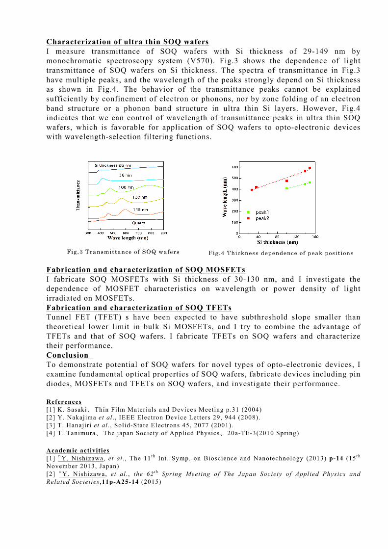
Characterization of ultra thin SOQ wafers I measure transmittance of SOQ wafers with Si thickness of 29-149 nm by monochromatic spectroscopy system (V570). Fig.3 shows the dependence of light transmittance of SOQ wafers on Si thickness. The spectra of transmittance in Fig.3 have multiple peaks, and the wavelength of the peaks strongly depend on Si thickness as shown in Fig.4. The behavior of the transmittance peaks cannot be explained sufficiently by confinement of electron or phonons, nor by zone folding of an electron band structure or a phonon band structure in ultra thin Si layers. However, Fig.4 indicates that we can control of wavelength of transmittance peaks in ultra thin SOQ wafers, which is favorable for application of SOQ wafers to opto-electronic devices with wavelength-selection filtering functions. Fabrication and characterization of SOQ MOSFETs I fabricate SOQ MOSFETs with Si thickness of 30-130 nm, and I investigate the dependence of MOSFET characteristics on wavelength or power density of light irradiated on MOSFETs. Fabrication and characterization of SOQ TFETs Tunnel FET (TFET) s have been expected to have subthreshold slope smaller than theoretical lower limit in bulk Si MOSFETs, and I try to combine the advantage of TFETs and that of SOQ wafers. I fabricate TFETs on SOQ wafers and characterize their performance. Conclusion To demonstrate potential of SOQ wafers for novel types of opto-electronic devices, I examine fundamental optical properties of SOQ wafers, fabricate devices including pin diodes, MOSFETs and TFETs on SOQ wafers, and investigate their performance. References [1] K. Sasaki、Thin Film Materials and Devices Meeting p.31 (2004) [2] Y. Nakajima et al . , IEEE Electron Device Letters 29, 944 (2008). [3] T. Hanajiri et al . , Solid-State Electrons 45, 2077 (2001). [4] T. Tanimura、The japan Society of Applied Physics、 20a-TE-3(2010 Spring) Academic activities [1] ⚪ ︎Y. Nishizawa, et al . , The 11th Int. Symp. on Bioscience and Nanotechnology (2013) p-14 (15th November 2013, Japan) [2] ⚪ ︎Y. Nishizawa, et al . , the 62th Spring Meeting of The Japan Society of Applied Physics and Related Societies ,11p-A25-14 (2015)
Fig.3 Transmittance of SOQ wafers Fig.4 Thickness dependence of peak positions