Design and characterization of a 30-GHz bandwidth low...
10
Design and characterization of a 30-GHz bandwidth low-power silicon traveling-wave modulator Ran Ding a,n , Yang Liu a , Qi Li b , Yisu Yang a , Yangjin Ma a , Kishore Padmaraju b , Andy Eu-Jin Lim c , Guo-Qiang Lo c , Keren Bergman b , Tom Baehr-Jones a , Michael Hochberg a,c,d a Department of Electrical and Computer Engineering, University of Delaware, Newark, DE, USA b Department of Electrical Engineering, Columbia University, 500 West 120th Street, New York, New York, USA c Institute of Microelectronics, Agency for Science, Technology and Research (AnSTAR), Singapore d Department of Electrical and Computer Engineering, University of Singapore, Singapore article info Article history: Received 22 August 2013 Received in revised form 28 January 2014 Accepted 29 January 2014 Available online 7 February 2014 Keywords: Silicon photonics Waveguide modulators Traveling-wave modulators Photonics integrated circuits abstract We present the design and characterization of a silicon PN junction traveling-wave Mach–Zehnder modulator near 1550 nm wavelength. The device shows 30 GHz bandwidth at 1 V reverse bias, with a 2.7 V-cm V π L π and accordingly a 9-V small-signal V π . The insertion loss of the phase shifter is 3.6 dB 70.4 dB. The device performance metrics in combination show significant improvement com- pared to the state-of-the-art in the sense that lower phase shifter loss and higher bandwidth are achieved for the same V π or vice versa. We demonstrated low modulation power of 640-fJ/bit at 40 Gb/s with a 1.6-V pp differential-drive and 0-V DC bias, raising the prospect of direct compatibility with CMOS drive-voltages. Critical design tradeoffs are analyzed and design models are validated with measurement results. We proposed a new figure-of-merit (FOM) V π L π R pn C 2 pn as the junction design merit for high- speed traveling-wave modulators, and utilized 6 implants to achieve an optimal FOM with lower insertion loss. Several key RF design issues are addressed for the first time using simulation and measurement results. In particular, we discussed bandwidth extension using mismatched termination and closely matched experimental results. A bandwidth-limiting RF multi-mode behavior is noted, which also exists in other results in the literature; we suggested a widely applicable design remedy. & 2014 Elsevier B.V. All rights reserved. 1. Introduction Silicon optical modulators [1] are critical for data communica- tion related applications [2–5] in silicon photonics. Over the past decade, significant progress has been made in this area, but achieving efficient high-speed modulation in silicon still proves to be challenging, mainly due to the weak electro-optic (EO) effects available in this material [5,6]. The fundamental and key modulator device metrics include insertion loss, device bandwidth, and EO modulation efficiency (for Mach–Zehnder modulators the efficiency is characterized by V π ). In addition, optical bandwidth, device footprint, temperature sensitivity, fabrication error tolerance and CMOS compatibility are also of great importance for practical designs, design scalability and possibility of CMOS monolithic integration [7,8]. A majority of the high-speed demonstrations thus far have been based on reverse-biased silicon PN junctions. Among these results, high-speed resonator modulators are promising in achiev- ing ultra-low modulation power consumption and compact device footprint. Recently, Li et al. demonstrated a 40 Gb/s 1 V-drive ring modulator [9], although a few issues remain to be fully addressed, such as limited optical bandwidth, and consequently necessary thermal drift stabilization as well as operating wavelength align- ment between devices. The other main category of carrier-depletion PN junction modulators is traveling-wave Mach–Zehnder (TWMZ) modulators. Although in academic demonstrations imbalanced Mach–Zehnder (MZ) modulators are often used (mostly for the convenience of testing), balanced MZ modulators are the true practical devices and have the key advantage of being temperature insensitive, thus do not require active thermal stabilization. Traveling-wave design enables the driving of a long phase-shifter at high speed, therefore can yield low voltage modulators. 40–60 Gb/s channel speed is a logical next step from existing 25–28 Gb/s data rates. The device we present here targets at Contents lists available at ScienceDirect journal homepage: www.elsevier.com/locate/optcom Optics Communications http://dx.doi.org/10.1016/j.optcom.2014.01.071 0030-4018 & 2014 Elsevier B.V. All rights reserved. n Corresponding author. E-mail address: [email protected] (R. Ding). Optics Communications 321 (2014) 124–133
Transcript of Design and characterization of a 30-GHz bandwidth low...

Design and characterization of a 30-GHz bandwidth low-power silicontraveling-wave modulator
Ran Ding a,n, Yang Liu a, Qi Li b, Yisu Yang a, Yangjin Ma a, Kishore Padmaraju b,Andy Eu-Jin Lim c, Guo-Qiang Lo c, Keren Bergman b, Tom Baehr-Jones a,Michael Hochberg a,c,d
a Department of Electrical and Computer Engineering, University of Delaware, Newark, DE, USAb Department of Electrical Engineering, Columbia University, 500 West 120th Street, New York, New York, USAc Institute of Microelectronics, Agency for Science, Technology and Research (AnSTAR), Singapored Department of Electrical and Computer Engineering, University of Singapore, Singapore
a r t i c l e i n f o
Article history:Received 22 August 2013Received in revised form28 January 2014Accepted 29 January 2014Available online 7 February 2014
Keywords:Silicon photonicsWaveguide modulatorsTraveling-wave modulatorsPhotonics integrated circuits
a b s t r a c t
We present the design and characterization of a silicon PN junction traveling-wave Mach–Zehndermodulator near 1550 nm wavelength. The device shows 30 GHz bandwidth at 1 V reverse bias, with a2.7 V-cm VπLπ and accordingly a 9-V small-signal Vπ. The insertion loss of the phase shifter is3.6 dB70.4 dB. The device performance metrics in combination show significant improvement com-pared to the state-of-the-art in the sense that lower phase shifter loss and higher bandwidth areachieved for the same Vπ or vice versa. We demonstrated low modulation power of 640-fJ/bit at 40 Gb/swith a 1.6-Vpp differential-drive and 0-V DC bias, raising the prospect of direct compatibility with CMOSdrive-voltages. Critical design tradeoffs are analyzed and design models are validated with measurementresults. We proposed a new figure-of-merit (FOM) VπLπRpnC
2pn as the junction design merit for high-
speed traveling-wave modulators, and utilized 6 implants to achieve an optimal FOM with lowerinsertion loss. Several key RF design issues are addressed for the first time using simulation andmeasurement results. In particular, we discussed bandwidth extension using mismatched terminationand closely matched experimental results. A bandwidth-limiting RF multi-mode behavior is noted, whichalso exists in other results in the literature; we suggested a widely applicable design remedy.
& 2014 Elsevier B.V. All rights reserved.
1. Introduction
Silicon optical modulators [1] are critical for data communica-tion related applications [2–5] in silicon photonics. Over the pastdecade, significant progress has been made in this area, butachieving efficient high-speed modulation in silicon still provesto be challenging, mainly due to the weak electro-optic (EO)effects available in this material [5,6].
The fundamental and key modulator device metrics includeinsertion loss, device bandwidth, and EO modulation efficiency(for Mach–Zehnder modulators the efficiency is characterized byVπ). In addition, optical bandwidth, device footprint, temperaturesensitivity, fabrication error tolerance and CMOS compatibility arealso of great importance for practical designs, design scalabilityand possibility of CMOS monolithic integration [7,8].
A majority of the high-speed demonstrations thus far havebeen based on reverse-biased silicon PN junctions. Among theseresults, high-speed resonator modulators are promising in achiev-ing ultra-low modulation power consumption and compact devicefootprint. Recently, Li et al. demonstrated a 40 Gb/s 1 V-drive ringmodulator [9], although a few issues remain to be fully addressed,such as limited optical bandwidth, and consequently necessarythermal drift stabilization as well as operating wavelength align-ment between devices.
The other main category of carrier-depletion PN junctionmodulators is traveling-wave Mach–Zehnder (TWMZ) modulators.Although in academic demonstrations imbalanced Mach–Zehnder(MZ) modulators are often used (mostly for the convenience oftesting), balanced MZ modulators are the true practical devicesand have the key advantage of being temperature insensitive, thusdo not require active thermal stabilization. Traveling-wave designenables the driving of a long phase-shifter at high speed, thereforecan yield low voltage modulators.
40–60 Gb/s channel speed is a logical next step from existing25–28 Gb/s data rates. The device we present here targets at
Contents lists available at ScienceDirect
journal homepage: www.elsevier.com/locate/optcom
Optics Communications
http://dx.doi.org/10.1016/j.optcom.2014.01.0710030-4018 & 2014 Elsevier B.V. All rights reserved.
n Corresponding author.E-mail address: [email protected] (R. Ding).
Optics Communications 321 (2014) 124–133

applications at these speeds or equivalently a device bandwidth ofapproximately 30 GHz [9–11]. In recent TWMZ results [10–15]however, it was often found that a similar bandwidth was onlyachieved with very short devices (�1 mm or less) as well as highbias voltages (frequently 3–5 V), both of which limit the modula-tion efficiency. High Vπ and associated high drive voltages increasepower consumption and make the devices less compatible withadvanced CMOS, which is usually constrained by low-breakdownvoltages. For long devices [14,15], in addition to smaller band-width, they were demonstrated with high insertion loss on thephase shifter making it difficult to fit in a practical system linkbudget. In summary, further device improvements remain to bemade for high-speed low voltage modulators with low loss.
In this paper, we present a 3-mm long, 30-GHz bandwidthdifferential-drive silicon TWMZ modulator based on a lateral PNjunction with low reverse bias. The phase shifter VπLπ is 2.7 V-cm(a small-signal Vπ of 9 V) and the insertion loss on the phaseshifter is only 3.6 dB. At similar bandwidth this device shows thelowest Vπ and lowest drive voltage requirement due to differen-tial-drive, or at similar Vπ it shows the highest bandwidth as wellas the lowest insertion loss on the active phase shifter [10–15]. Thecombined device metrics show significant improvement comparedto the state of the art. The main part of the paper is organized asthe following. Section 2 describes the fabrication process, identi-fies key design tradeoffs and presents design details of the device.Section 3 presents the measurement results, compares them tosimulation results to validate the design model and providesdiscussions about several RF effects regarding TWMZ design thatwere not addressed in previous publications.
2. Device design and fabrication
2.1. Fabrication process
The device presented in this work was fabricated at theInstitute of Microelectronics (IME)/AnSTAR [17] through an OpSISMulti-Project Wafer (MPW) run [18]. The fabrication process wasvery similar to that in [16] with the main difference being that inthis work we employed six implant layers instead of four in silicon,and they were: lightly doped P and N for forming the junction inthe waveguide core, intermediate density Pþ and Nþ for reducingseries resistance without inducing excessive optical loss, andheavily doped Pþþ and Nþþ implant for low resistance siliconfar away from the waveguide and for forming low resistancemetal-to-silicon contact – no silicidation was used in the fabrica-tion process, the contact was formed directly between aluminumand heavily doped silicon. The traveling-wave phase shifter cross-section is illustrated in Fig. 1 and the microscope photo of thefabricated device is shown in Fig. 3(b). The wafer was an 8"Silicon-on-Insulator (SOI) from SOITEC with 220 nm top silicon,
2 μm buried oxide layer and 750Ω-cm high resistive siliconsubstrate. The silicon slab thickness was 90 nm and ridge wave-guide width was 500 nm. The top metal Aluminum was used forthe traveling-wave electrodes, and it was 2 μm thick, mostlysituated above dielectric materials in the back-end stack. Othermetal and dielectric material properties and thicknesses as well asfabrication steps were identical as they were in [16].
2.2. Overall device design considerations
In this section we briefly review the TWMZ design model andpresent useful design tradeoff relations to facilitate further dis-cussions in this paper. The cross-section of the TWMZ shown inFig. 1 is considered as a PN junction loaded transmission line andits equivalent circuit model is schematized in Fig. 2. Rtlðf Þ is thefrequency-dependent metal skin resistance in Ω/m, and has a
ffiffiffif
p
dependence in principle, Ctl and Ltl are the capacitance andinductance between the metal traces in the units of F/m andH/m respectively. Cpn is the PN junction capacitance (in F/m); thetotal amount of silicon series resistance from the electrodes to theedges of the junction depletion region is captured in Rpn (in Ω-m).We further define the junction intrinsic RC bandwidth asf rc ¼ 1=ð2πRpnCpnÞ and approximate the device impedanceas Zdev ¼
ffiffiffiffiffiffiffiffiffiffiffiffiffiffiffiffiffiffiffiffiffiffiffiffiffiffiffiffiLtl=ðCtlþCpnÞ
p, which is accurate when the frequency is
well below the intrinsic RC bandwidth, i.e. f =f rc⪡1. It is worthnothing that, due to the use the high-resistivity substrate, thesubstrate conductance due to transverse current flow can beneglected in the frequency range of interest [29].
The bandwidth of a TWMZ modulator is mostly determined bythe RF loss due to Rpn, if RF and optical velocities are closelymatched. To make this clear we can look at the overall RF fieldloss coefficient (in the unit of Neper/m), which can be expressedas [19]
α¼ αmetalþαsilicon
� 12Rtlðf ÞZdev
þ2π2f 2RpnC2pnZdev
1þðf =f rcÞ2ð1aÞ
¼ 12Rtlðf ÞZdev
þ πf 2CpnZdev
f rcð1þðf =f rcÞ2Þð1bÞ
Where αmetal and αsilicon are the loss due to metal seriesresistance and lateral silicon resistance respectively. Let us referto the first term as Rtl loss and the second term as Rpn loss. At highfrequencies, the second term usually dominates because of its f 2
dependence, whereas Rtl(f) has affiffiffif
pdependence. Incidentally, this
can be seen clearly in Fig. 4(g), a simulation plot of the actualdevice under discussion.
For the moment, let us assume perfect velocity match andneglect other non-ideal RF effects (such as reflection, multi-modalbehavior etc.), a straightforward relation between EO 3dB band-width f EO;3 dB and achievable device length Ldev can be derivedas [20]:
1�e�αðf EO;3 dBÞLdev
αðf EO;3 dBÞLdev¼ 1
ffiffiffi2
p ) αðf EO;3 dBÞLdev ¼ 0:74Neper ¼ 6:4 dB ð2ÞFig. 1. Simplified device cross-section, not to scale.
Fig. 2. Schematic of the simplified equivalent circuit of the PN junction loadedtransmission line.
R. Ding et al. / Optics Communications 321 (2014) 124–133 125

This is the “6 dB” rule-of-thumb frequently referred to inpublications about TWMZ, i.e. the RF 6 dB (more accurately6.4 dB) bandwidth is close to the EO response 3 dB bandwidth.
For the sake of simplicity let us further assume the desiredbandwidth fEO,3 dB is sufficiently low compared to the intrinsic RCbandwidth of the junction so that ðf EO;3dB=f rcÞ2⪡1. Usually theTWMZ design is in the “low loss” regime of the transmission linemodel where this assumption naturally stands. Inserting Eq. 1 intoEq. 2, and we get
Ldev ¼0:74
ð1=2ÞRmetalðf EO;3 dBÞ=Zdevþ2π2f 2EO;3 dBRpnC2pnZdev
ð3aÞ
� 0:74
2π2f 2EO;3 dBZdev
1
RpnC2pn
¼ 0:74
πf 2EO;3 dBZdev
f rcCpn
ð3bÞ
The approximation before arriving at Eq. 3a is based on that Rpnloss is much larger than Rtl loss at frequencies near f EO;3 dB.
A few scaling trends can be derived from Eqs. 3a and 3b, whichquantify the tradeoffs in the seemingly complicated design space:
(I) It becomes apparent that getting low Vπ at high frequencyis increasingly difficult, since Ldevp1=f 2EO;3 dB, consequentlyVπ � ðVπLπÞ=Ldevp f 2EO;3 dB.
(II) In general, to design for certain impedance and bandwidththe achievable device length Ldev and Vπ have the following scalingtrends with respect to PN junction parameters:
Ldevp1=ðRpnC2pnÞ;Vπp ðVπLπÞRpnC
2pn ð4Þ
Obviously, a reduction in Rpn is directly reflected in a reductionin Vπ (for certain bandwidth design target). Highlighted in Eq. 4 isanother key point. In an attempt to improve junction modulationefficiency (reducing VπLπ) the factor ðVπLπÞRpnC
2pn should be
evaluated. A reduction in VπLπ is likely to come at the cost ofincreased Cpn. An increase in ðVπLπÞRpnC
2pn implies that the reduc-
tion in VπLπ does not ultimately lead to the reduction of the deviceVπ. Therefore, a low doped, low capacitance density junction couldbe a more advantageous for traveling-wave design, which is thecase of the design reported in this paper.
(III) Designing at lower device impedance Zdev is advantageous,because Ldevp1=Zdev;VπpZdev, holding junction parameters con-stant. Note that the impedance Zdev is not the terminationimpedance but the RF impedance of device itself. The effect oftermination impedance on device performance will be addressedin Section 3.2. Assuming the device is in fact terminated with Zdev,we can then conveniently evaluate the drawback of using lowimpedance design, which is mainly some loss of the incomingdrive voltage, if the driver is at impedance Z0 that is higher thanZdev. The ratio of voltage dropped on the device ðVdevÞ versus thedriver output voltage ðV0Þ is Vdev=V0 ¼ 2Zdev=ðZdevþZ0Þ. For exam-ple, this voltage-intake factor is 67% for a 25Ω device terminatedwith 25Ω driven by a 50Ω driver. However, the achievable devicelength at 25Ω is approximately twice as it would be for a 50Ωdesign based on Eqs. 3a,b, therefore overall the 25Ω design wouldbe more advantageous. The device length doubling is of course arough estimate, due to the omission of metal loss.
It is also worth noting that single-drive push-pull modulators[21] demonstrated an elegant way to ease the design of 50Ωdevice impedance while conveniently maintaining matched RFand optical velocities. Due to halving the junction capacitiveloading to the transmission line electrode, the bandwidth-limiting Rpn loss is approximately halved (according to Eq. 1b,keeping f rc constant) and therefore very long devices are possibleat high speeds. However, doubled device length combined withsingle-drive operation yields approximately the same drive voltagerequirement as it is for a conventional differential-drive TWMZdevice, while doubling the device length implies high opticalinsertion loss, which is a drawback that needs to be weighedagainst the benefits associated with such single-drive designs.
2.3. PN junction design
The waveguide PN junction phase shifter is the core componentof an MZ modulator; its metrics largely determine the achievableoverall device performance, as shown in Eq. 3a,b and Eq. 4. Inaddition to providing a low ðVπLπÞRpnC
2pn factor, the PN junction
design also needs to achieve low optical insertion loss.We chose lightly doped P and N to form the junction in the
waveguide with the P side average doping concentration beingaround 5�1017/cm3 and N side being close to 3�1017/cm3.
Fig. 3. (a) RF layout dimensions (b) Device microscope photograph.
R. Ding et al. / Optics Communications 321 (2014) 124–133126

The junction line was designed to be at the center of thewaveguide, with no intentionally added intrinsic region width.This low-doped PN junction is in favor of the efficiency versus losstradeoff, characterized by the figure-of-merit FdB-V (in dBnV) asdefined in [22]. Also, it helped achieve a low ðVπLπÞRpnC
2pn by
maintaining a low Cpn and competitive VπLπ.To achieve a low Rpn with low loss, we employed a 3-level side-
doping configuration as illustrated in Fig. 1, with carefully chosendoping density and doping profile. We selected Pþ and Nþdoping density of 2�1018/cm3 and 3�1018/cm3 respectively andoptimized the doping profile. The onset of doping to the edge ofthe waveguide is defined as “clearance”. The clearance of Pþ andNþ doping were 120 nm and 140 nm respectively. The Pþþ andNþþ doping were on the level of 1�1020/cm3 and their clearancewere both 950 nm and the doped region extended laterally untilthey reached the electrode contact regions that were 3.95 μm
away from the edge of the waveguide. A breakdown of optical lossand resistance of the various regions is presented in Table 1 below.
Based on implantation process modeling and device simulation[23], Cpn was 280 fF/mm at 0 V and 220 fF/mm at �1 V bias, thusf rc at �1 V bias reached 100 GHz. The simulated small-signal VπLπwas 1.7 V-cm at �1 V bias.
2.4. Traveling-wave electrode design
In light of the observation (III) in the end of Section 2.1, wecontinued to use a 33–37Ω impedance design similar to [16]instead of designing at 50Ω. This is also a convenient impedanceto design with our junction capacitance Cpn while achievingvelocity matching condition and low RF loss. Another considera-tion was that if the device were properly terminated with match-ing impedance, this device would still provide an acceptable
Fig. 4. (a–f) Simulated unloaded TL (solid line) and junction-loaded TL with 0 V bias (solid line with dots), the frequency axis range is set to 2–38 GHz to eliminate artificialsimulation data processing errors and (g) Simulated RF loss of the device under investigation, Case1 is based on simulated Cpn and Rpn and Case2 is based on measurement-corrected Cpn and Rpn.
R. Ding et al. / Optics Communications 321 (2014) 124–133 127

S11 (o�10 dB), when tested in 50Ω environment or integratedwith 50Ω drivers.
However, we do not deem it a fundamental requirement tocomply with 50Ω standard RF interfaces, because eventually andespecially for on-chip applications the TWMZ devices are likely beclosely integrated with custom drivers, in which cases the shortlength (or even zero length) electrical connection as well as theavailability of custom designed low impedance drivers wouldmake it possible to freely choose any impedance as long as itadvances the overall device and system performance. For example,numerous laser drivers have been designed at very low impe-dances [24] for efficient driving.
The device layout and microscopic photograph is shown inFig. 3. We used a Ground-Signal (GS) coplanar transmission lineelectrode to drive each arm. The GS lines have 50 μm trace widthand 5 μm gap. The length of the phase shifter is 3 mm. Theseparation between the two arms is 400 μm center-to-center.Metal tiling exist around the device to comply with density designrules, the clearance between metal tiling and the RF traces is75 μm. The traces used the 2 μm thick aluminum layer (M2) in theprocess. The layout of the via-stack from M2 down to silicon wasmainly determined by design rules and considerations to achievesufficiently low resistances for vias and metal-to-silicon contacts.The detailed PN junction and side doping configurations weredescribed in Section 2.3. It is worth noting that the phase shifter inthe actual TWMZ only has �90% of its length loaded with PNjunction, due to striation as illustrated in Fig. 3(a). The striation indoping was to ensure the current flows in the metal traces towardthe wave propagation direction, as opposed to flowing in thesilicon.
At the driving end (the right side in Fig. 3(b)), a GSGSG pad setwas used to deliver differential driving signal to the device. Atransition was made on chip from GSG to GS. At the terminationend (the left side in Fig. 3(b)), a GSSGSSG pad set was used,offering four 50Ω ports. All pad pitches are 100 μm. The G pads inthe termination pad set are connected together by the lower levelmetal (M1), which is not very visible in the photograph. Eachdevice arm was associated with two 50Ω ports in parallel,allowing 25Ω termination through a GSSGSSG RF probe and off-chip resistors. Other values of termination impedance would be
less convenient, but is possible to implement by bonding thephotonics chip to a high-speed printed circuit board (PCB) viashort-length bond wires, and using surface-mount low parasiticresistors on the PCB. On the other hand, the GSSGSSG padset allowed us to take the RF S-parameter as discussed in detailin Section 3.2.
Simulated RF characteristics of the transmission line electrodeswith and without PN junction loading is presented in Fig. 4 (a)–(f).First, the metal traces were simulated in HFSS [25], and thenloaded line characteristics were calculated based on the circuitmodel in Fig. 1(b). The presented curves that involve PN junction,i.e. the dotted traces in Fig. 4 (e) and (f) and the entire plot ofFig. 4(g), were calculated at 0 V bias condition and with the 90%junction loading factor taken into account. Near 30 GHz,Rtl is8.1Ω/mm, Ltl is 420 pH/mm, and Ctl is 120 pF/mm. Loaded withPN junction, the impedance is 34Ω and RF index is 3.78 at 30 GHz.The RF loss is presented in Fig. 4(g) with the total loss, and loss dueto Rtl and Rpnplotted separately and it is clear that Rpn loss is thedominating source of RF loss at high frequencies. In this plot Case1 trace was obtained with simulated Rpn and Cpn, i.e. 7.2Ω-mm,and 280 fF/mm, whereas Case 2 was using 15Ω-mm and 230 fF/mmto approximate the measured device. The increase in Rpninfabricated device is mainly attributed to the higher sheet resis-tance in the light P and N doping as well as higher contactresistance from metal to Pþþ doped silicon, which will bediscussed in Section 3.
3. Measurement results and discussions
3.1. DC VπLπ and insertion loss
We first measured the optical transmission and DC perfor-mance of the device. The optical test setup used an Agilent81980 A tunable laser and an 81636B detector to record the devicetransmission spectra. The intentional imbalance of the device was100 μm and the free spectral range was about 5.7 nm. We trackedthe null in the spectrum to generate phase shift versus appliedvoltage on one arm, from which VπLπs was calculated. The resultsare shown in Fig. 5. Incidentally, there are some ambiguity and
Table 1Optical loss and resistance breakdown
N and P doped waveguide core N and P doped slab region Nþ doped slab region Pþ doped slab region Nþþ and Pþþ doped region Total
R IL R IL R IL R IL R IL R ILSimulation 1.5 6.8 1.6 1.1 0.97 2.5 0.53 0.49 0.01 7.2 8.3
Notes: “R” denotes resistance in Ω-mm, “IL” denotes insertion loss in dB/cm. The IL reported for waveguide core includes the loss of N and P doped slab region due tosimulation setting. IL numbers only include free carrier absorption loss at 0 V bias, and do not include intrinsic waveguide loss.
Fig. 5. (a) Optical spectra versus applied voltage (b) VπLπ versus applied voltage.
R. Ding et al. / Optics Communications 321 (2014) 124–133128

discrepancy about the definition of VπLπ in the literature. One wayto report VπLπ is based on an actual π phase shift [26,27]. This testprotocol requires devices of various lengths to get a VπLπ versus Vπ(or Lπ) curve and could be difficult for short devices (high voltages).Here we adopted an alternative approach: the VπLπ versus appliedvoltage relation is generated by the measurement of the phaseshift Δϕdut versus applied voltage Vapplied on one phase shifter ofcertain length Ldut , and simply VπLπ ¼ π
ΔϕVappliedLdut . The curve VπLπversus Vapplied is basically VπLπ versus Vπ. This approach waswidely used in publications on silicon modulators, includingseveral in the references list, for example [11], [13], [14], and [24].
At �1 V bias the measured phase shifter VπLπ was 2.7 V-cm.Further measurements over 5 different chips showed a gooduniformity. Taking into account the 90% loading factor, the VπLπof a fully doped waveguide phase shifter would be 2.43 V-cm,higher than the simulated 1.7 V-cm. The measured Cpn was 230 fF/mmat 0 V and 190 fF/mm at -1 V bias for a fully doped waveguidephase shifter, lower than the simulated value 280 fF/mm at 0 Vand 220 fF/mm at �1 V. We further measured silicon resistorswith various doping types, doping concentrations and siliconthicknesses, and revealed that Pþþ or Nþþ doped siliconresistance agreed with simulation within 5%. However, Pþ orNþ doped silicon showed �30% higher resistance than simula-tion, and P or N doped resistance showed �50% higher resistancethan simulation. Combining the higher VπLπ, lower Cpn and higherresistance of P or N doped silicon resistance, we suspect thediscrepancies could be due to: physically applied implantationdose being smaller than simulated, and possible incompleteionization of the dopant. Other fabrication inaccuracies are harderto be verified or excluded.
The on and off chip coupling were through grating couplers.The device insertion loss was obtained by comparing the max-imum transmission of the MZ spectrum to a grating coupler loopto de-embed the coupler insertion loss. Then the routing wave-guide loss was subtracted, and we arrive at the device insertionloss of 6.2 dB that consist of two simple Y-junctions and the phaseshifter. We note that the Y-junction in this particular device wasnot carefully designed and has a high insertion loss of 1.3 dB each.Therefore the loss due to the phase shifter was only 3.6 dB(averaged from multiple chips with a standard deviation of0.37 dB). The reduction of the loss in Y-junction would bestraightforward, because recently a 0.3 dB insertion loss optimizedY-junction with uniform yield was demonstrated and was fabri-cated in the same batch of wafers [28].
The 3.6 dB70.37 dB phase shifter insertion loss can be brokendown as follows. The waveguide intrinsic loss was measured to be1.9870.29 dB/cm from 5 samples on the same wafer, i.e. a �0.6 dBcontribution to the phase shifter loss. Therefore the various dopants(junction and side doping) introduced 3.0 dB70.38 dB loss. Con-sidering the 90% loading coefficient, we can back calculate the freecarrier absorption loss was 11.171.5 dB/cm, whereas the simulatedvalue is 8.3 dB/cm. The discrepancy could be excess loss due to Pþand Nþ misalignment error (the 3s of the overlay accuracy was alarge fraction of the doping clearance) or a slight change inwaveguide dimensions inducing change in optical mode overlapwith Pþ and Nþ dopants. Incidentally, we measured PN junctiondoped waveguides that are without the side doping Pþ , Nþ , Pþþand Nþþ . The measured free carrier loss was 6.3 dB/cm on average,which was very close to the simulated 6.8 dB/cm. This made it morelikely the extra loss seen in the TWMZ phase shifters was due to Pþ ,Nþ doping etc.
3.2. Small-signal bandwidth measurement
The EO frequency response of the TWMZ was characterizedusing an Agilent 67 GHz Vector Network Analyzer (VNA), and an
U2T XPDV3120R-VF-VP 70 GHz bandwidth photodetector. The EOS21 is presented in Fig. 6. This measurement was done throughon-wafer probing with a 40 GHz rated Cascade ACP GSGSG drivingprobe and a 20 GHz rated Cascade Unity GSSGSSG probe with off-chip resistors for 25Ω termination. The VNA drove only onedevice arm at a time; the unused arm was properly terminatedat both the driving and termination end with 50Ω and 25Ωrespectively. This “full-termination” scheme closely resembles theactual operating condition of a differential drive modulator. Theprobes were not de-embedded from the frequency response andthe RF S21 roll-off of the GSGSG probe was 0.5 dB near the devicebandwidth. Reverse bias was applied through the bias-tee inthe VNA.
30 GHz bandwidth was achieved for both arms at 1 V reversebias. The signal-to-noise ratio is better than 10 dB near thebandwidth. The same bandwidth was almost reached with 0 Vbias (a long plateau in the EO S21 coincided with the �3 B linebetween 23 GHz and 30 GHz). We observed two distinctivefeatures of the EO S21: the peaking near 5 GHz and the notchnear 17 GHz. These two features were consistently observed acrossmany devices on both arms. We will explain them based on RFmeasurements.
The RF S-parameter measurements were done with the 40 GHzGSGSG probe at the driving side with one GSG port connected toVNA Port 1 and the other GSG port attached to 50Ω to terminatethe unused arm. At the termination end, a 40 GHz GSSG probe wasused with one GS port connected to VNA Port 2 and one GS portattached to 50Ω. It presents 25Ω to the modulator arm undertest and receives RF through signal. We had to leave the termina-tion end of the untested arm open due to the lack of a high speedGSSGSSG probe. The RF calibration included the cabling but couldnot include the probes, due to the lack of a GSG-to-GS calibrationsubstrate. The uncalibrated probes were responsible for the fine-pitch ripples on the S-parameters traces, most visible on S11 dueto their low magnitude. The measurement results are shown inFig. 7(a).
First of all, we can use RF S11 and S21 to back calculate the RFindex and RF loss. The RF index can be obtained bynrf ¼ c=ð2Lef fΔf Þ, where c is the speed of light in vacuum, Lef f isthe effective RF length (it is the device length with small correc-tions to take into account of the input and termination wiring thathas an RF index of roughly 2.5, Lef f is estimated to be 3.3 mm basedon simulation), andΔf the spacing of S11 null locations (measuredto be 12 GHz). Therefore RF index was calculated to be 3.8, and isclose to the optical group index 3.9.
To calculate RF loss and RF 6.4 dB bandwidth, we should notethat the measured RF S21 starts at�3.9 dB rather than close to0 dB. This was due to the 50Ω-driving, 25Ω-termination testingconfiguration, which results in a 67% voltage-intake at lowfrequencies (see Section 2.1). In principle it should be �3.5 dB,
Fig. 6. EO S21 at 0 V and �1 V bias.
R. Ding et al. / Optics Communications 321 (2014) 124–133 129
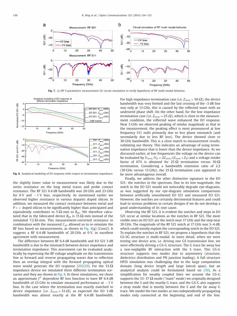
the slightly lower value in measurement was likely due to theseries resistance on the long metal traces and probe contactresistance. The RF S21 6.4 dB bandwidth was 20 GHz and 23 GHzfor 0 V and �1 V bias, respectively. As mentioned earlier weobserved higher resistance in various dopants doped silicon. Inaddition, we measured the contact resistance between metal andPþþ doped silicon to be significantly higher than anticipated andequivalently contributes to 5Ω-mm to Rpn. We therefore calcu-lated that in the fabricated device Rpn is 15Ω-mm instead of thesimulated 7.2Ω-mm. This measurement-corrected resistance incombination with the measured Cpn allowed us to re-simulate theRF loss based on measurements, as shown in Fig. 4(g) (Case2). Itsuggests a RF 6.4 dB bandwidth of 20 GHz at 0 V, in excellentagreement with measurement.
The difference between RF 6.4 dB bandwidth and EO S21 3 dBbandwidth is due to the mismatch between device impedance andtermination impedance. This assessment can be evaluated analy-tically by expressing the RF voltage amplitude on the transmissionline as forward and reverse propagating waves due to reflectionthen an overlap integral with the forward propagating opticalwave would generate the EO response [20],[29]. For the 33Ωimpedance device we simulated three different termination sce-narios and they are shown in Fig. 8. In these simulations, we chosean approximate f 2 dependent RF loss function to have RF 6.4 dBbandwidth of 23 GHz to emulate measured performance at �1 Vbias. In the case where the termination was exactly matched todevice impedance (i.e. Zterm ¼ 33Ω), as expected the EO 3 dBbandwidth was almost exactly at the RF 6.4 dB bandwidth.
For high impedance termination case (i.e. Zterm ¼ 50Ω), the devicebandwidth was very limited and the last crossing of the -3 dB linewas only at 13 GHz, this is caused by the reflected wave with anundesired phase shift. On the other hand, for the low impedancetermination case (i.e. Zterm ¼ 25Ω), which is close to the measure-ment condition, the reflected wave enhanced the EO response.Near 5 GHz we observed peaking of similar magnitude as that inthe measurement, the peaking effect is most pronounced at lowfrequency S11 nulls primarily due to less phase mismatch (andsecondarily due to less RF loss). The device showed close to30 GHz bandwidth. This is a close match to measurement results,validating our theory. This indicates an advantage of using termi-nation impedance that is lower than the device impedance. As wediscussed earlier, at low frequencies the voltage on the device canbe evaluated by Vterm=V0 ¼ 2Zterm=ðZtermþZ0Þ and a voltage-intakefactor of 67% is obtained for 25Ω termination versus 50Ωtermination. Considering a bandwidth extension ratio of 2.2(30 GHz versus 13 GHz), the 25Ω termination case appeared tobe more advantageous overall.
Finally, we address the other distinctive signature in the EOS21: the notches in the spectrum. Due to its low magnitude, thenotch in the EO S21 would not noticeably degrade eye-diagrams,as was suggested by our eye-diagram simulation comparisonsbetween artificially smoothened EO S21 and measured EO S21.However, the notches are certainly detrimental features and couldlead to serious problems in certain designs if we do not develop agood understanding of its root cause.
Observing the RF S21, it is evident the notches and steps in EOS21 occur at similar locations as the notches in RF S21. The mostvisible ones on EO S21 are the notch near 17 GHz and the step near30 GHz. The magnitude of the RF S21 notch at 17 GHz was 3–4 dB,which could mostly explain the corresponding notch in the EO S21.To explain the notches in RF S21, we propose a hypothesis that theGS-SG structure is multi-modal. In more detail, when we weretesting one device arm, i.e. driving one GS transmission line, wewere effectively driving a GS-G structure. The G trace far away hasa non-negligible RF interaction with the S trace. This GS-Gstructure supports two modes due to asymmetry (structure,dielectrics distribution and PN junction loading). A full structureHFSS simulation was challenging due to the large computationdomain (long device length and large lateral span), but ananalytical analysis could be formulated based on [30]. As asimplification for weakly coupled lines we assume the GS-Gsupports the 33–37Ωmode (“main”mode) we originally designedbetween the S and the nearby G trace, and the GS-G also supportsa stray mode that is mostly between the S and the far away Gtrace. We model the two modes as two independently propagatingmodes only connected at the beginning and end of the line.
Fig. 7. (a) RF S-parameters measurement (b) circuit simulation to verify hypothesis of RF multi-modal behavior.
Fig. 8. Analytical modeling of EO response with respect to termination impedance.
R. Ding et al. / Optics Communications 321 (2014) 124–133130

The combined line was driven by a 50Ω source and terminated by25Ω. We used the TWMZ parameters described earlier for themain mode, and estimated the capacitance between the S traceand the far away G trace is Cstray¼�20 fF/mm, using two-wiretransmission line equations [19]. To avoid complicated circuit models,we picked reasonable constant metal skin resistance as opposed to afrequency-dependent multi-resistor-inductor network (which isresponsible for the large simulation errors in S21 notch amplitudeand S11 amplitude and null location). But, our simple modelappeared to be sufficient as a qualitative validation [31]. Using acircuit simulator [32], we obtained the traces in Fig. 7(b) with strayinductance between S and side G as Lstray¼4.2 nH/mm. Qualitatively,Fig. 7(b) agrees well with Fig. 7(a), and validates our multi-modalhypothesis.
In light of this observation we further comment that, notches inRF S21 were observed in previous demonstrations of TWMZmodulators that were based on a GSG layout (or a GSGSG layoutby combining two GSG arms), where the PN junction was loadedonly in one of the two GS slots. Examples include Fig. 5 in [11],Fig. 9 in [12], Fig. 4 in [14] and likely Fig. 4 in [13]. Manydemonstrations did not present EO or RF S21, therefore it isdifficult to have a more complete summary. But, according toour simulations in HFSS of a few relatively compact GSG mod-ulator structures, notches were usually present in RF S21. It is verylikely that the notches in these demonstrations are due to multi-modal RF behavior as well: the one-side junction loading makesthe GSG structure highly asymmetric in a similar fashion as the GS-G
structure we discussed above and this RF multi-modal property isexpected to exhibit detrimental effect given that the device issufficiently long and/or the testing frequency is sufficiently high.
A simple remedy to both the GSG structure and GS-G structureis that one needs to periodically tie together the groundplanes that are on both sides of the S trace, so that effectivelythere is only one large ground plane interacting with the S trace,ensuring only one RF mode is supported between S and G. Thespacial period of the “G-tie” should be much smaller than the beatlength of the lowest two eigenmodes of the originally multi-modestructure.
3.3. Eye-diagrams
We further demonstrated high-speed eye-diagrams with dif-ferential drive. The available sample for the eye-diagram measure-ments exhibited similar Vπ and EO S21 bandwidth as reported inprevious sections. The measurement was set up as following. Apair of differential 40 Gb/s 215�1 pseudorandom binary sequence(PRBS) was generated by a Centellax TG1P4A PRBS source, ampli-fied by a pair of Centellax OA4MVM3 driver amplifiers, and thenattenuated by passive attenuators (rated for DC—23 GHz) to thedesired amplitude before being applied to the device under testthrough a Cascade 40 GHz rated GSGSG probe. DC bias voltageswere applied to each modulator arm through bias tees insertedbefore the attenuators. The device probing and termination con-figuration were the same as the EO S-parameter measurements,
Fig. 9. (a) a typical electrical eye-diagram of the driving signals (b)–(d): optical eye-diagrams at 40 Gb/s with differential-drive: (b) 0 V bias and 1.6Vpp drive voltage, 3.1 dBextinction ratio was achieved with bias loss of 1.4 dB. (c) 0.25 V reverse bias and 2.5 Vpp drive voltage, 5.1 dB extinction ratio was achieved with bias loss of 1.7 dB. (d) 3 Vreverse bias and 4.7Vpp drive voltage, 7.1 dB extinction ratio was achieved with bias loss of 0 dB. Scales are different in (b)–(d).
R. Ding et al. / Optics Communications 321 (2014) 124–133 131

with slightly different cabling. The optical output of the device waspassed through an Erbium Doped Fiber Amplifier (EDFA), anoptical bandpass filter with 3.5 nm bandwidth and then sent tothe optical module (Agilent 86109B) of an Agilent 86100B digitalcommunication analyzer (DCA).
We report on eye-diagrams with different drive voltages andmodulator bias losses in Fig. 9(b)–(d). The bias loss is the excessloss due to modulator biasing, to quantify how much the bit “1”optical output is below the maximum transmission. For example,3 dB bias loss means bit “1” is at the quadrature point. Thedifferential drive voltage signals before connected to the GSGSGprobe were verified by electrical eye-diagram measurements,based on which we can accurately report the drive voltages in a50Ω test environment. A typical 40 Gb/s electrical eye-diagram ofthe driving signal is shown in Fig. 9(a). The actual drive voltagereceived by the device is slightly lower than the reported drivevoltage due to the voltage-intake factor that we discussed before.We observed a slight output asymmetry of the electrical amplifiersand attenuators on the two data paths, but the difference waswithin 5%, and we report the averaged drive voltage values below.
Using a 1.6Vpp drive voltage and 0 V DC bias, 3.1 dB extinctionwas achieved with a very low 1.4 dB bias loss, as shown in Fig. 9(b).The power consumption can be calculated as following. At animpedance of 50Ω, an ideal 1.6Vpp NRZ signal centered at 0 Vcarries 12.8 mWof power. At 40 Gb/s, the energy per bit is 640fJ/bit.Due to the availability of test equipment only 40 Gb/s operationwas demonstrated, although we expect the device to be capable ofpassing higher data rate bit streams based on simulations, whichwould result in further reduction of energy per bit.
The achievable extinction ratio (ER) in the eye-diagrams can betraded off with drive voltage and bias loss. For example, with a2.5Vpp drive voltage and a 0.25 V revere bias, 5.1 dB extinction wasobtained with 1.7 dB bias loss, as shown in Fig. 9(c); with a 4.7Vpp
drive voltage and a 3 V revere bias, 7.1 dB extinction was obtainedwith 0 dB bias loss, as shown in Fig. 9(d) The observed ER is lowerthan anticipated based on the phase shifter static performance(phase shift and dynamic loss versus applied voltage). The reducedextinction and reduced eye vertical opening is partly due to thelimited bandwidth in the testing system in addition to the deviceitself. The electrical eye-diagrams mentioned above measured thedrive signal immediately before the RF probe connected to thedevice, that is it included the PRBS source, amplifiers, bias tees,attenuators and cables. From the electrical eye-diagram in Fig. 9(a),we measured a 10–90% rise time of roughly 15 ps, which amountsto approximately 23 GHz bandwidth and leaves a tight margin forthe device. In addition to the limited system bandwidth, opticalnoise due to the EDFA further degraded the eye opening. Incontrast, we recently demonstrated a modulator with similar RFlayout at 1300 nm with the testing done at a different testingfacility where higher speed components were available and EDFAwas not used [33]. 50 Gb/s open eye-diagrams were demonstratedwith similarly low drive voltages, suggesting the 40 Gb/s eye-diagram quality is highly dependent on and likely limited by ourtest equipment.
4. Conclusions
To summarize, in this paper we address the design andcharacterization of a high performance silicon PN junctiontraveling-wave Mach–Zehnder modulator. The key underlyingdesign tradeoffs are identified and incorporated into the devicedesign. A device is then presented with significant performanceimprovement compared to the state of the art.
A PN junction design should maintain a low ðVπLπÞRpnC2pn factor
to enable low Vπ with high device bandwidth. Modulation
efficiency needs to trade effectively with optical loss, indicatedby the FdB-V figure-of-merit. For both considerations we choselightly doped PN junction with optimized 3-level side doping.
We have shown that lower device impedance is advantageousfor overall device performance, and a 33–37Ω device impedancewas chosen for the TWMZ design. Having termination impedancelower than the device impedance has benefit in terms of band-width extension while only incurring modest voltage loss.A bandwidth extension factor of 2.2 was achieved while thevoltage-intake factor was maintained at a reasonable 67%. Multi-modal RF behavior is proposed and qualitatively verified to be thepossible cause for the S21 notches observed in our device as wellas several recent GSG modulator demonstrations. A remedy issuggested to combat this. Therefore, performance enhancementand impairment are both possible with respect to the RF designaspect of a TWMZ device, and 6.4 dB RF bandwidth is not always agood indicator of 3 dB EO response bandwidth.
A 3 mm long 30 GHz bandwidth differential-drive TWMZmodulator is demonstrated with 1 V reverse bias. The deviceexhibits a small-signal Vπ of 9 V and has a low 3.6 dB insertionloss on the phase shifters. 40 Gb/s eye-diagrams were demon-strated, and 640 fJ/bit energy per bit was achieved with 1.6Vpp
drive voltage and no DC bias; higher data rates were expected tobe possible although not demonstrated due to the limitation oftest equipment. Compared to the state of the art, at similarbandwidth this device shows the lowest Vπ and lowest drivevoltage requirement due to differential-drive, or at similar Vπ itshows the highest bandwidth as well as the lowest insertion losson the active phase shifter. The combined device metrics showsignificant improvement compared to the state of the art. Takinginto account of the fabrication imperfections, the device behaviorwas accurately described by device models.
Acknowledgements
The authors gratefully acknowledge support from an AFOSRSTTR grant (FA9550–12-C-0038) and NRF Fellowship NRF2012NRF-NRFF001-143. The authors would also like to thank GernotPomrenke, of AFOSR, for his support of the OpSIS effort, throughboth a PECASE award (FA9550-13-1-0027) and ongoing fundingfor OpSIS (FA9550-10-l-0439). The authors gratefully acknowledgethe loan of critical equipment for this project from AT&T.
Reference
[1] G.T. Reed, G. Mashanovich, F.Y. Gardes, D.J. Thomson, Nat. Photonics 4 (8)(2010) 518.
[2] R.A. Soref, IEEE. J. Sel. Top. Quantum Electron. 12 (6) (2006) 1678.[3] B. Jalali, M. Paniccia, G. Reed, IEEE Microw. Mag. 7 (3) (2006) 58.[4] D.A.B. Miller, Proc. IEEE 97 (7) (2009) 1166.[5] A.V. Krishnamoorthy, R. Ho, X. Zheng, H. Schwetman, J. Lexau, P. Koka, G. Li,
I. Shubin, J.E. Cunningham, Proc. IEEE 97 (7) (2009) 1337.[6] R.A. Soref, B.R. Bennett, IEEE J. Quantum Electron. 23 (1) (1987) 123.[7] L.C. Kimerling, D. Ahn, A.B. Apsel, M. Beals, D. Carothers, Y. -K. Chen, T. Conway,
D.M. Gill, M. Grove, C. -Y. Hong, M. Lipson, J. Liu, J. Michel, D. Pan, S.S. Patel,A.T. Pomerene, M. Rasras, D.K. Sparacin, K. -Y. Tu, A.E. White, C.W. Wong, Proc.SPIE 6125 (2006) 6.
[8] C. Gunn, Micro. IEEE 26 (2) (2006) 58–66.[9] G. Li, X. Zheng, H. Thacker, J. Yao, Y. Luo, I. Shubin, K. Raj, J. E. Cunningham,
A. V. Krishnamoorthy, in: Proceedings of 2012 IEEE 9th International Group IVPhotonics, Institute of Electrical and Electronics Engineers, San Diego, 2012,pp. 1–3.
[10] L. Liao, A. Liu, D. Rubin, J. Basak, Y. Chetrit, H. Nguyen, R. Cohen, N. Izhaky,M. Paniccia, Electron. Lett. 43 (22) (2007) 1196.
[11] X. Xiao, H. Xu, X. Li, Z. Li, T. Chu, Y. Yu, J. Yu, Opt. Express 21 (4) (2013) 4116.[12] F.Y. Gardes, D.J. Thomson, N.G. Emerson, G.T. Reed, Opt. Express 19 (12) (2011)
11804.[13] D. Thomson, F. Gardes, J. Fedeli, S. Zlatanovic, Y. Hu, B. Kuo, E. Myslivets,
N. Alic, S. Radic, G.Z. Mashanovich, G.T. Reed, IEEE Photon. Technol. Lett. 24(2012) 234.
R. Ding et al. / Optics Communications 321 (2014) 124–133132

[14] M. Ziebell, D. Marris-Morini, G. Rasigade, J.M. Fédéli, P. Crozat, E. Cassan,D. Bouville, L. Vivien, Opt. Express 20 (10) (2012) 10591.
[15] D.J. Thomson, F.Y. Gardes, Y. Hu, G. Mashanovich, M. Fournier, P. Grosse,J.-M. Fedeli, G.T. Reed, Opt. Express 19 (12) (2011) 11507.
[16] T. Baehr-Jones, R. Ding, Y. Liu, A. Ayazi, T. Pinguet, N.C. Harris, M. Streshinsky,P. Lee, Y. Zhang, A.E.-J. Lim, T.-Y. Liow, S.H.-G. Teo, G.-Q. Lo, M. Hochberg, Opt.Express 20 (11) (2012) 12014.
[17] T.-Y. Liow, K.-W. Ang, Q. Fang, J.-F. Song, Y.-Z. Xiong, M.-B. Yu, G.-Q. Lo, D.-L. Kwong, IEEE J. Sel. Top. Quantum Electron. 16 (1) (2010) 307.
[18] OpSIS, ⟨http://opsisfoundry.org⟩.[19] D.M. Pozar, 2nd,Microwave Engineering, 2, John Wiley & Sons, Chap, 1998.[20] Liu Jia-Ming, Photonic Devices, 6, Cambridge University Press, Chap, 2005.[21] P. Dong, L. Chen, Y.-K. Chen, Opt. Express 20 (6) (2012) 6163.[22] X.G. Tu, T.Y. Liow, J.F. Song, M.B. Yu, G.Q. Lo, Opt. Express 19 (19) (2011) 18029.[23] Sentaurus TCAD Tools Suite, Synopsys.[24] S. Galal, B. Razavi., IEEE J. Solid-State Circuits 38 (12) (2003) 2138.
[25] Ansoft HFSS, Ansoft Corporation.[26] N.-N. Feng, S. Liao, D. Feng, P. Dong, D. Zheng, H. Liang, R. Shafiiha, G. Li,
J.E. Cunningham, A.V. Krishnamoorthy, M. Asghari, Opt. Express 18 (8) (2010)7994.
[27] J. Ding, H. Chen, L. Yang, L. Zhang, R. Ji, Y. Tian, W. Zhu, Y. Lu, P. Zhou, R. Min,M. Yu, Opt. Express 20 (7) (2012) 7081.
[28] Y. Zhang, S. Yang, A. Lim, G. Lo, C. Galland, T. Baehr-Jones, M. Hochberg, Opt.Express 21 (2013) 1310.
[29] Y. Hui, W. Bogaerts, J. Lightw. Technol. 30 (11) (2012) 1602.[30] V.K. Tripathi, IEEE Trans. Microw. Theory Tech. 23 (9) (1975) 734.[31] F. Merget, S. Azadeh, J. Mueller, B. Shen, M. Nezhad, J. Hauck, J. Witzens, Opt.
Express 21 (2013) 19593.[32] Virtuoso Spectre Circuit Simulator, Cadence Design Systems.[33] M. Streshinsky, R. Ding, Y. Liu, A. Novack, Y. Yang, Y. Ma, X. Tu, E.K. S. Chee,
A.E.-J. Lim, P.G.-Q. Lo, T. Baehr-Jones, M. Hochberg, Opt. Express 21 (2013)30350.
R. Ding et al. / Optics Communications 321 (2014) 124–133 133