Design and analysis of HVDC switch gear station for … · Design and analysis of HVDC switch gear...
65
Design and analysis of HVDC switch gear station for meshed HVDC grid Project of Science PATRICIA SERRANO JIMÉNEZ Department of Energy and Environment Division of Electric Power Engineering CHALMERS UNIVERSITY OF TECHNOLOGY Göteborg,¨ Sweden 2013
Transcript of Design and analysis of HVDC switch gear station for … · Design and analysis of HVDC switch gear...

Design and analysis of HVDC switch gear
station for meshed HVDC grid
Project of Science
PATRICIA SERRANO JIMÉNEZ Department of Energy and Environment Division of Electric Power Engineering CHALMERS UNIVERSITY OF TECHNOLOGY Göteborg,¨ Sweden 2013


Design and analysis of HVDC switch gear station
for meshed HVDC grid
Project of Science
PATRICIA SERRANO JIMÉNEZ
Department of Energy and Environment Division of Electric Power Engineering CHALMERS UNIVERSITY OF TECHNOLOGY Göteborg,¨ Sweden 2013


Design and analysis of HVDC switch gear
Station for meshed HVDC grid PATRICIA SERRANO JIMÉNEZ
© Patricia Serrano Jiménez, May, 2013.
Department of Energy and Environment Division of Electric Power Engineering Chalmers University of Technology SE–412 96 Goteborg¨ Sweden Telephone +46 (0)31–772 100


Abstract I
ABSTRACT
It is of fundamental interest to avoid faults in a DC grid due to the severely of these events.
However, the faults are unavoidable, so in a fault case is necessary to act fast.
The protection in a DC grid comprises a key component, the HVDC breaker. For this reason in
this thesis, a simulation is programmed in order to be able to study the HVDC breaker
operation, distinguishing between normal and fault operation. Matlab is the program used in
this work, and an initial simulation is tested firstly to choose which method is the most
appropriate.
Once the circuit behaviour is studied, some tactics to improve the performance of the
system are proposed, focusing on thermal losses.
The principal results (current waveforms and energy dissipation) show that introducing some
modifications into the system like using more IGBTs in parallel or changing the inductance
values, it is possible to get a feasible DC breaker.
To sum up, this report will present one tool being able to simulate different configurations
and to study the results, besides some suggestions how to make the system more efficient.
Keywords: HVDC Breaker, IGBT

Acknowledgements II
ACKNOWLEDGEMENTS
I would like to express my special appreciation to Prof. Torbjorn Thiringer for providing me
the opportunity to work in this project and for all support guidance and encouragement
during the same.
I am also grateful for the support I have received from my family. Especially from my older
brother, Daniel, without his help during all my degree anything would have been possible.
Moreover, my gratitude goes to my friends, Isabel and Veronica, who have shared with me
unforgettable moments. .
Finally, I have no words to appropriately thank Javier for his invaluable support and
understanding. He has been my strength.

CONTENTS
Abstract ................................................................................................................................................................................... I
Acknowledgements ............................................................................................................................................................ II
List of symbols ...................................................................................................................................................................... V
Chapter 1, Introduction .................................................................................................................................................... 1
HVDC vs HVAC .......................................................................................................................................................... 1
PREVIOUS WORK .................................................................................................................................................... 2
THESIS OBJECTIVE ................................................................................................................................................... 3
Chapter 2, Collection of known usable theory ......................................................................................................... 5
SYSTEM DESIGN REQUIREMENTS ..................................................................................................................... 5
IGBT ............................................................................................................................................................................. 6
PROPOSED HYBRID IGBT BREAKER .................................................................................................................. 7
Chapter 3, Case set-up.................................................................................................................................................... 12
OPERATION PROCESS ......................................................................................................................................... 12
S-FUNCTION METHOD ........................................................................................................................................ 15
SIMPOWERSYSTEMS METHOD ....................................................................................................................... 19
Chapter 4, Analysis Part ................................................................................................................................................. 22
IDEAL CASE ............................................................................................................................................................. 22
S-function method .................................................................................................................................... 23
Simpowersystems method .................................................................................................................... 24
Comparison of methods ......................................................................................................................... 26
REAL CASE ............................................................................................................................................................... 27
Add more IGBTs in parallel ................................................................................................................... 30
Advance the trigger time in the main branch ................................................................................ 32
Decrease the inductance values .......................................................................................................... 34
Chapter 5, Conclusions ................................................................................................................................................... 37
RESULT FROM PRESENT WORK ...................................................................................................................... 37
FUTURE WORK ...................................................................................................................................................... 38
References .......................................................................................................................................................................... 40
Appendix ............................................................................................................................................................................. 41
S-function code real case ....................................................................................................................... 41
Simpowersystem code ideal case ....................................................................................................... 50

Contents 4

List of symbols V
LIST OF SYMBOLS
IGBT Insulated Gate Bipolar Transistor
Vce Collector-emitter voltage
Vge Gate-emitter voltage
Vgg Gate-gate voltage
Ic Collector current
iaux Auxiliary current
ibreak Main current
Itotal Total current
Zth Thermal impedance

List of symbols 6

Design and analysis of HVDC switch gear station for meshed HVDC grid | Chapter 1 1
CHAPTER 1
INTRODUCTION
The development of alternative energy sources using renewable energy is an important
environmental step. Offshore wind energy is one of the major upcoming sources of energy.
DC transmission can be preferred in an offshore power transmission due to the reactive
power limitation of long AC power transmissions. However DC transmission presents a
difficult behaviour when a short-circuit fault occurs, due to the fact that the current has no
zero crossing, and also a relatively low impedance due to absence of ωL reactance. The fault
penetration is thus deeper in a DC grid. In order to handle this effect, it is necessary to have
fast and reliable HVDC breakers to isolate faulted parts. In order to prevent unwanted
consequences in the rest of the grid, it is necessary to clear the fault as quick as possible.
HVDC VS HVAC
The electricity started to be used for energy transporting approximately 120 years ago, and
the first HVDC link was put into operation 50 ago. So HVDC can be considered to be a
consolidated technology, although in a continuous development due to the improvements in
the power electronic area.
When it comes time to choose between HVAC and HVDC in energy transmission, some few
aspects have to be taken in account:
Technical aspects
o In an HVCD system the power in the system power is almost kept constant,
independently of the distance. However, in an HVAC system, the transmission
capacity decreases with the distance, due to inductive effects.
o In the case of having two systems, with different frequencies at the ends, it is
unavoidable to use HVDC.
o The energy transmission used in offshore cables is limited to short distances in
HVAC, due to its high dielectric capacity. So in an offshore system, it is
necessary the use HVDC. HVDCs are not affected by capacitive neither
inductive parameter of the lines.

Chapter 1 | Introduction
Introduction 2
Economic aspects
o In general, the HVDC system has more direct costs than HVAC. However these
costs are compensated for lower costs in the line transmission and less losses.
Environmental aspects
o The principal environmental reasons for which HVDC is preferable instead of
HVAC, besides the visual impact, are reasons related to the magnetic field and
the corona discharge.
PREVIOUS WORK
The faults are important incidents, which have been dealt with in several studies. Different
ways for acting in a fault case have been presented in several thesis works.
For instance Lena Max's thesis presents that the increase of the wind power penetration in
the electrical system has introduced new requirements to ensure a good operation of the
grid. Wind farms should not be disconnected during a fault in the main grid. Since the power
transmission to the grid decrease dramatically during the fault, the excess energy should be
dissipated in order to avoid tripping of the wind farm and preventing an over voltage. The
whole collection grid of the wind park was allowed to collapse for about 1 second.
One of the solutions is to reduce the output power of the wind turbines by using an internal
breaker resistance or letting the excess energy be stored as rotational energy. The other
solution is the use of a breaker resistance at the HVDC link. Whit this solution the DC
collection grid will not be affected during grid faults, since the DC collection grid will not be
affected.
However, this strategy is not possible in a meshed DC grid, here a fault must be cleared,
without a collapse in the network voltage. (MAX, 2009)

Chapter 1 | Introduction
Introduction 3
THESIS OBJECTIVE
This thesis is a part of an ongoing work at the department of Energy and Environment
regarding a meshed DC network equipped with wind energy installations. The goal of this
work is to simulate a short-circuit fault in order to propose settings of the DC breaker, as well
as the design, and to check that the operation is as expected.
The simulation will be accomplished by modelling the circuit in Matlab. This modelling will be
done by two different methods: using S-function and SimPowerSystems.

Chapter 1 | Introduction
4
Design and analysis of HVDC switch gear station for meshed HVDC grid | Chapter 2 5
CHAPTER 2
COLLECTION OF KNOWN USABLE THEORY
SYSTEM DESIGN REQUIREMENTS
A DC grid can be considered when more than two converter stations are interconnected on
the DC side via DC cables or overhead lines in meshed or radial system.
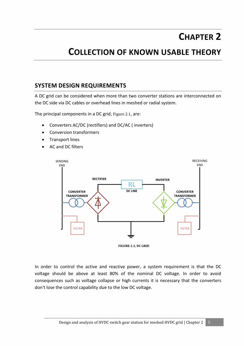
The principal components in a DC grid, Figure 2.1, are:
Converters AC/DC (rectifiers) and DC/AC ( inverters)
Conversion transformers
Transport lines
AC and DC filters
DC LINE
RLRECTIFIER INVERTER
CONVERTERTRANSFORMER
FILTER
SENDINGEND
CONVERTERTRANSFORMER
FILTER
RECEIVINGEND
FIGURE 2.1, DC GRID
In order to control the active and reactive power, a system requirement is that the DC
voltage should be above at least 80% of the nominal DC voltage. In order to avoid
consequences such as voltage collapse or high currents it is necessary that the converters
don't lose the control capability due to the low DC voltage.
Chapter 2 | Collection of known usable theory
Collection of known usable theory 6
A DC short-circuit fault is the worst case, which can make the DC voltage to suddenly be
reduced to zero at the fault location. The effect of this voltage reduction can be reflected at
other places of the DC grid depending mainly on the electrical distance to the fault location.
In order not to disturb converter stations, the fault has to be cleared within 5ms, for a DC
grid connected by DC cables (JÜRGEN HÄFNER, 2011).
However, it is not only the DC grid system performance that requires fast DC switches, from
the DC breaker design point it is also very crucial to realize a fast fault current breaking.
IGBT
The insulated-gate bipolar transistor or IGBT is a three-terminal power semiconductor
device, and its most relevant characteristics are efficiency and fast switching.
The IGBT combines the simple gate-drive characteristics of the MOSFETs with the high-
current and low-saturation-voltage capability of bipolar transistors by combining an isolated
gate FET for the control input, and a bipolar power transistor as a switch, in a single device.
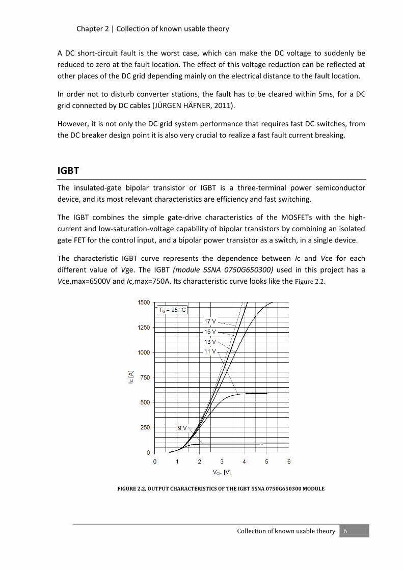
The characteristic IGBT curve represents the dependence between Ic and Vce for each
different value of Vge. The IGBT (module 5SNA 0750G650300) used in this project has a
Vce,max=6500V and Ic,max=750A. Its characteristic curve looks like the Figure 2.2.
FIGURE 2.2, OUTPUT CHARACTERISTICS OF THE IGBT 5SNA 0750G650300 MODULE

Chapter 2 | Collection of known usable theory
Collection of known usable theory 7
Another important factor of the IGBTs is its thermal behaviour. In order to determine the
temperature increase in the IGBT, it is necessary to know the thermal impedance. This
thermal impedance is described in the data-sheet through the characteristic curve, Figure 2.2.
FIGURE 2.3, THERMAL IMPEDANCE VS TIME
ΔT= 60 °C is defined as the maximum temperature increase allowed. This limit establishes a
value with which the IGBT can operate without being damaged.
PROPOSED HYBRID IGBT BREAKER
The purpose of this section is to illustrate the topology of the circuit used and the expected
operation in normal operation as well as during the fault condition.
The circuit consists mainly of a piece of the DC network, including its line parameter and a
hybrid DC breaker, and it is presented in the Figure 2.4.
The hybrid DC Breaker consists of two parallel branches: the auxiliary DC breaker and the
main DC breaker, with corresponding control circuits.

Chapter 2 | Collection of known usable theory
Collection of known usable theory 8
U1 U2
R1 L1
L2
L3
breaker
IGBT1-----> Vce1
Vce2-----> IGBT40
interp2filterVgg
iaux
interp2filterVgg
ibreak
AUXILIARY DRIVE CIRCUIT
AUXILIARY DC BREAKER
MAIN DC BREAKER
MAIN DRIVE CIRCUIT
HYBRID DC BREAKER
FIGURE 2.4, DC BREAKER CIRCUIT TOPOLOGY
During normal operation the auxiliary branch is conducting, but the IGBT (equivalent to
40IGBTs together) in the main branch is also prepared for operation, Figure 2.5. There is no
current in the main branch, but the main IGBT will start to conduct when the voltage level
over it reaches a certain value.
U1 U2
R1 L1
L2
L3
breaker
IGBT1-----> Vce1
Vce2-----> IGBT40
iaux
ibreak
Itotal
Auxiliary control circuit
Control signal
Main control circuit
Control signal
FIGURE 2.5, DC BREAKER IN NORMAL OPERATION

Chapter 2 | Collection of known usable theory
Collection of known usable theory 9
When a fault occurs, the auxiliary current raises fast. In the moment when the voltage over
the main IGBT reaches this certain value, a commutation current starts to flow between both
branches, Figure 2.6.
U1 U2
R1 L1
L2
L3
breaker
IGBT1-----> Vce1
Vce2-----> IGBT40
iaux
ibreak
Itotal
Commutation current
fault
Auxiliary control circuit
Control signal
Main control circuit
Control signal
FIGURE 2.6, COMMUTATION CURRENT
When the auxiliary current is zero, the breaker is opened and all the current flows through
the main branch, Figure 2.7.
U1 U2
R1 L1
L2
L3
breaker
IGBT1-----> Vce1
Vce2-----> IGBT40
iaux
ibreak
Itotal
fault
Auxiliary control circuit
Control signal
Main control circuit
Control signal
FIGURE 2.7, DC BREAKER WITH A FAULT CONDITION

Chapter 2 | Collection of known usable theory
Collection of known usable theory 10
The IGBT drive circuits have the following design, Figure 2.8:
Vgg
R
C Vge
FIGURE 2.8, DRIVE CIRCUIT

Chapter 2 | Collection of known usable theory
Collection of known usable theory 11

Design and analysis of HVDC switch gear station for meshed HVDC grid | Chapter 3 12
CHAPTER 3
CASE SET-UP
OPERATION PROCESS
During normal operation (pre-fault operation), the current will only flow through the
auxiliary branch.
The function of the mechanical breaker is to open the circuit when a fault appears. However,
the mechanical breaker only can act properly when the current is approximately zero. Due to
that the IGBT presence in the auxiliary branch is necessary. This IGBT is going to be
represented by a DC controllable voltage source and its needed control circuit.
When a fault occurs, the current increases fast in the auxiliary branch, and when this current
reaches a limit current value, a trigger signal is activated. Then Vge1 is decreased gradually
through the drive circuit, from its initial value to zero, Figure 3.1.
FIGURE 3.1, VGE VS TIME AUXILIARY DRIVE CIRCUIT
0.1 0.2 0.3 0.4 0.5 0.6 0.70
5
10
15
20
25
Time [ms]
Vge
[V
]
Vge1

Chapter 3 | Case set-up
Case set-up 13
This value and iaux are the inputs to the Vce function. The Vce function has been stored as a
look-up table using the characteristics of the IGBT.
This function then interpolates with the current and Vge, and provides a Vce value for each
instant, Figure 3.2.
interp2filterVgg
iaux
breaker
FIGURE 3.2, AUXILIARY DRIVE CIRCUIT
As a result of that, there is an increase in Vce1 and a decrease in the current. When the
current is negligible, the mechanical breaker can open this branch.
At the same time, the current is to be commutated to the main branch, in order to bring the
current in the auxiliary branch to zero.
This branch has a similar configuration to the one used in the auxiliary DC breaker, but now
there is no mechanical breaker, instead, inside of the Vce function there are 40 IGBTs in
series.
The main drive circuit will be activated with a separate trigger and gate-emitter voltage.
Now, instead of decreasing the current, all the current has to flow through this branch. For
this reason, Vge2 will be increased through its drive circuit, from its initial value to a
maximum. This new trigger signal has to be activated a little bit later than the trigger signal
in the auxiliary branch.
Furthermore, as soon as iaux is zero, this new trigger signal will be activated again, but in the
opposite way, decreasing Vge2, from its maximum value to zero, Figure 3.3. The voltage over
the 40 IGBTs will now increase to such a high value that the whole main current, ibreak, can
fall to zero, the fault has now been cleared.

Chapter 3 | Case set-up
Case set-up 14
FIGURE 3.3, VGE VS TIME MAIN DRIVE CIRCUIT
Both drive circuit operations are shown in the Figure 3.4
FIGURE 3.4, VGE VS TIME MAIN AND AUXILIARY DRIVE CIRCUITS
0.1 0.2 0.3 0.4 0.5 0.6 0.7 0.8 0.9 10
2
4
6
8
10
12
14
16
18
20
Time [ms]
Vge
[V
]
Vge2
0 0.1 0.2 0.3 0.4 0.5 0.6 0.7 0.8 0.90
5
10
15
20
Time [ms]
Vge
[V
]
Vge1
Vge2

Chapter 3 | Case set-up
Case set-up 15
S-FUNCTION METHOD
This method consists of the sequence presented in Figure 3.5:
CALCULATE TIME OF NEXT SIMPLE HIT
INITIALIZATE MODEL
CALCULATE OUTPUTS
UPDATE DISCRETE STATES
CALCULATE OUTPUTS
LOCATE ZERO CROSSINGS
CALCULATE DERIVATIVES
AT TERMINATION PERFORM ANY REQUIRED TASKS
CALCULATE DERIVATIVESSim
ula
tio
n lo
op
Integratio
n
FIGURE 3.5, OVERVIEW OF S-FUNCTION

Chapter 3 | Case set-up
Case set-up 16
Now it is time to formulate the equations for the circuit, Figure 3.6.
U1 U2
R1 L1
L2
L3
breaker
IGBT1-----> Vce1
Vce2-----> IGBT40
iaux
ibreak
Itotal
FIGURE 3.6, CIRCUIT TOPOLOGY
By performing a KVL the relation between voltage and current in the auxiliary branch can be
found as,
(3.1)
Doing the same with the main branch gives
(3.2)
and between both branches,
(3.3)
(3.4)
(3.5)

Chapter 3 | Case set-up
Case set-up 17
where
(3.6)
(3.7)
Combining the equations produces the following expresions
(3.8)
(3.9)
Renaming the inductances
(3.10)
(3.11)
The final equations become:
(3.12)
(3.13)

Chapter 3 | Case set-up
Case set-up 18
The equation for the drive circuits, Figure 3.7, can be formulated as:
Vgg
R
C Vge
FIGURE 3.7, DRIVE CIRCUIT
(3.14)
(3.15)
(3.16)
(3.17)
The final equation can now be set up
(3.18)

Chapter 3 | Case set-up
Case set-up 19
SIMPOWERSYSTEMS METHOD
Simpowersystems provides fundamental building blocks to implement the circuit. With these
blocks, which represent the different elements, and the physical connections it is possible to
develop the system.
The circuit representation by this method looks like Figure 3.8
FIGURE 3.8, SIMPOWERSYSTEMS MODEL
Where the inside of the auxiliary DC breaker system is the circuit represented in the Figure 3.9
FIGURE 3.9, AUXILIARY DC BREAKER

Chapter 3 | Case set-up
Case set-up 20
And its control circuit, Figure 3.10
FIGURE 3.10, AUXILIARY CONTROL CIRCUIT
As well as inside the main DC breaker system, Figure 3.11
FIGURE 3.11, MAIN DC BREAKER
With its control circuit, Figure 3.12
FIGURE 3.12, MAIN CONTROL CIRCUIT

Chapter 3 | Case set-up
21

Design and analysis of HVDC switch gear station for meshed HVDC grid | Chapter 4 22
CHAPTER 4
ANALYSIS PART
In this section the main results from the simulation is presented.
It is divided in two parts. The first corresponds to an ideal case, which will be simulated by
the two methods (Simpowersystems and S-function).
The second part is a simulation with parameters corresponding to a real DC cable, which will
be simulated only using the S-function method.
IDEAL CASE
In this case one ideal DC cable has been chosen. Its characteristics are presented in Table 4.1
TABLE 4.1, IDEAL DC CABLE CHARACTERISTICS
Single-core cables, nominal voltage 4 kV
Branch inductances (L1, L2)
Inductance Impedance
H H Ω
0.001 0.001 0.25
The main results correspond to the current waveform, where is possible to check if the
behaviour is the expected, and the power representation, which is used to calculate the
energy dissipation.

Chapter 4 | Analysis Part
Analysis Part 23
S-FUNCTION METHOD
The current waveforms are presented in Figure 4.1
FIGURE 4.1, CURRENT VS TIME S-FUNCTION METHOD
The power over both IGBTs are shown in Figure 4.2
FIGURE 4.2, AUXILIARY AND MAIN POWER VS TIME S-FUNCTION METHOD
0 0.5 1 1.5 2 2.50
100
200
300
400
500
600
700
800
900
Time [ms]
Cu
rren
t [A
]
iaux
ibreak
Itotal
0 0.5 1 1.5 2 2.50
0.5
1
1.5
2
2.5
3
3.5
4
4.5
Time [ms]
Pow
er [M
W]
power1
power2

Chapter 4 | Analysis Part
Analysis Part 24
The main results are presented in Table 4.2
TABLE 4.2, IDEAL S-FUNCTION RESULTS
Imax Power max 1 Energy 1 Power max 2 Energy 2
600.0815 A 2.999 MW 447.5634 J 4.255 MW 3214.9 J
SIMPOWERSYSTEMS METHOD
The current waveforms, Figure 4.3
FIGURE 4.3, CURRENT VS TIME S-FUNCTION METHOD
0 0.5 1 1.5 2 2.50
100
200
300
400
500
600
700
800
900
Time [ms]
Cu
rren
t [A
]
iaux
ibreak
Itotal

Chapter 4 | Analysis Part
Analysis Part 25
and the power over both IGBTs in Figure 4.4
FIGURE 4.4, AUXILIARY AND MAIN POWER VS TIME S-FUNCTION METHOD
The main results are presented in Table 4.3
TABLE 4.3, IDEAL SIMPOWERSYSTEMS RESULTS
Imax Power max 1 Energy 1 Power max 2 Energy 2
600.8 A 3.002 MW 448.951 J 4.255 MW 3188.1 J
0 0.5 1 1.5 2 2.50
0.5
1
1.5
2
2.5
3
3.5
4
4.5
Time [ms]
Pow
er [M
W]
power1
power2
Chapter 4 | Analysis Part
Analysis Part 26
COMPARISON OF METHODS
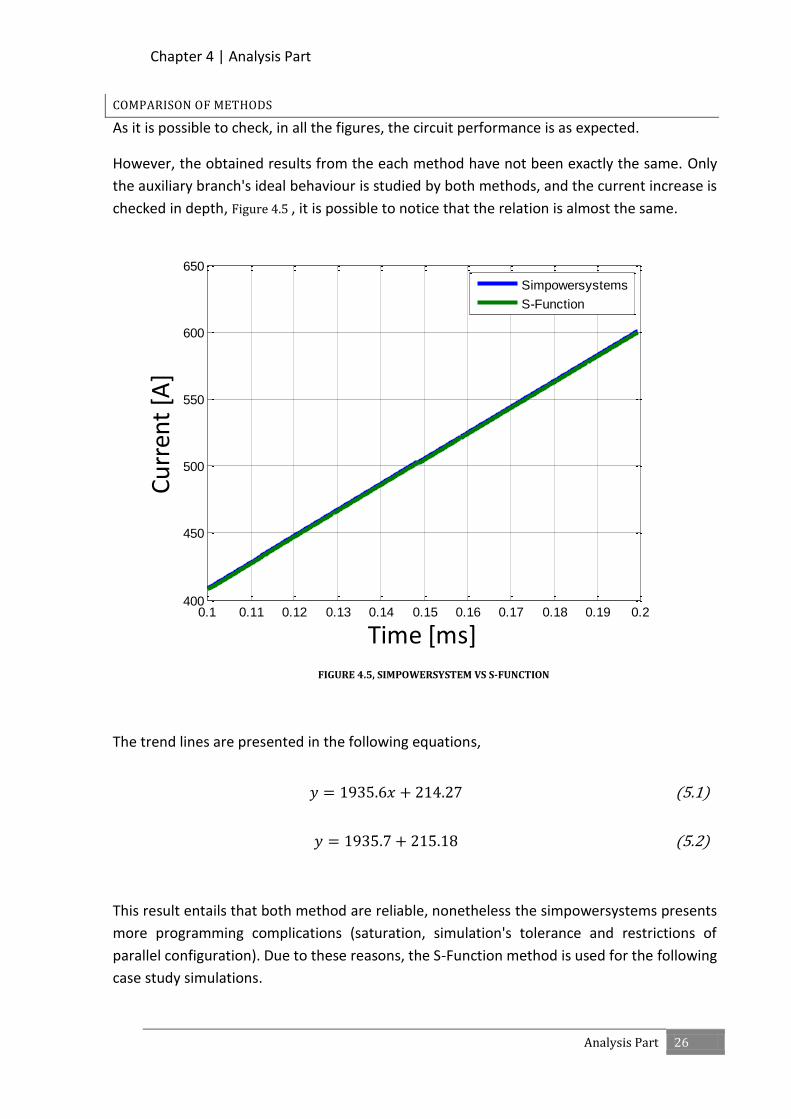
As it is possible to check, in all the figures, the circuit performance is as expected.
However, the obtained results from the each method have not been exactly the same. Only
the auxiliary branch's ideal behaviour is studied by both methods, and the current increase is
checked in depth, Figure 4.5 , it is possible to notice that the relation is almost the same.
FIGURE 4.5, SIMPOWERSYSTEM VS S-FUNCTION
The trend lines are presented in the following equations,
(5.1)
(5.2)
This result entails that both method are reliable, nonetheless the simpowersystems presents
more programming complications (saturation, simulation's tolerance and restrictions of
parallel configuration). Due to these reasons, the S-Function method is used for the following
case study simulations.
0.1 0.11 0.12 0.13 0.14 0.15 0.16 0.17 0.18 0.19 0.2400
450
500
550
600
650
Time [ms]
Cu
rren
t [A
]
Simpowersystems
S-Function

Chapter 4 | Analysis Part
Analysis Part 27
REAL CASE
In this case one real DC cable has been chosen from the data-sheet (ABB)
The resistance value is not given, so it must be calculated,
(5.3)
where
ρ: conductivity of copper
A: cross-section of conductor
The characteristics are presented in Table 4.4
TABLE 4.4, REAL DC CABLE CHARACTERISTICS
Single-core cables, nominal voltage 70 kV
Cross-section of conductor
Branch inductances (L1, L2)
Inductance Impedance
mm2 H mH/km mΩ/km
2000 0.001 0.29 8.5
* The length of the cable simulated is 500km
The real line inductance for a length of 500 km is 0.145H. However, this value is too high, and
the simulation presents some complications (slower simulation and more time necessary to
clear the fault). One solution to decrease this value could be simulating a shorter cable, but
the problem is that also the resistance would be affected with this method. A low resistance
value has an effect on the current, which will be higher and it will be necessary to have more
IGBTs. So, the decision taken is to implement the circuit with the original resistance and a
lower inductance value. So, the decision taken is to implement the circuit with the original
resistance and a lower inductance value. This value is 0.145mH, which is more similar to the
branch inductances, and a good response is obtained a good response that allows the study
of different settings.
The nominal voltage is now 70kV instead of 4kV as in the ideal case. This voltage increase has
an effect on the current, which is higher now. For this reason it is necessary to modify the
initial configuration. The current levels, Figure 4.6, impose to add 13 IGBT in parallel at least.
So the final configuration is one IGBT in series and 14 in parallel in the auxiliary branch, and
20 in series with 14 in parallel in each in the main branch.

Chapter 4 | Analysis Part
Analysis Part 28
FIGURE 4.6, CURRENT VS TIME S-FUNCTION METHOD
The power over both IGBTs are shown in Figure 4.7
FIGURE 4.7, AUXILIARY AND MAIN POWER VS TIME S-FUNCTION METHOD
0 0.2 0.4 0.6 0.8 1 1.2 1.40
1000
2000
3000
4000
5000
6000
7000
8000
9000
10000
Time [ms]
Cu
rren
t [A
]
iaux
ibreak
Itotal
0 0.2 0.4 0.6 0.8 1 1.2 1.40
10
20
30
40
50
60
Time [ms]
Pow
er [M
W]
power1
power2

Chapter 4 | Analysis Part
Analysis Part 29
The main results are presented in Table 4.5
TABLE 4.5, MAIN RESULTS
Imax Power max 1 Energy 1 Power max 2 Energy 2
5509.8 A 31.34 MW 2673.7 J 53.49 MW 19934 J
Analysing the thermal response is obtained that during 188μs the average power in the
auxiliary IGBT is
(5.4)
Extrapolating this value for 1ms, Zth=0.0004 K/W (module 5SNA 0750G650300) and the
power is 2.6737 MW. With these values is possible to calculate the temperature increase.
(5.5)
As is possible to check, this value is too far from the limit. The conclusion is that even though
this is the best configuration, it is not efficient if the thermal losses are considered.
In order to reduce the temperature increase it is necessary to reduce the current. For getting
this objective three possible changes will be studied:
1. Add more IGBTs in parallel
2. Advance the trigger time in the main branch
3. Decrease the inductance values

Chapter 4 | Analysis Part
Analysis Part 30
ADD MORE IGBTS IN PARALLEL
Since each IGBT has a Zth=0.0004 K/W and the temperature limit increase is 60 °C, the
maximum power is
(5.6)
This Zth corresponds to 1ms, so if this value is extrapolated, the maximum energy allowed is
(5.7)
This energy value is obtained by using 242 IGBTs at least.
The current waveforms look like Figure 4.8
FIGURE 4.8, CURRENT VS TIME S-FUNCTION METHOD
0 0.2 0.4 0.6 0.8 1 1.2 1.40
1000
2000
3000
4000
5000
6000
7000
8000
9000
10000
Time [ms]
Cu
rren
t [A
]
iaux
ibreak
Itotal

Chapter 4 | Analysis Part
Analysis Part 31
and the power representation is shown in Figure 4.9
FIGURE 4.9, AUXILIARY AND MAIN POWER VS TIME S-FUNCTION METHOD
The main results are presented in Table 4.6
TABLE 4.6, MAIN RESULTS
Imax Power max 1 Energy 1 Power max 2 Energy 2
5507.4 A 1.785 MW 150.0305 J 3.118 MW 1170.4 J
Analysing the thermal response, as is done in the previous case, is obtained that during
185μs the average power in the auxiliary IGBT is
(5.8)
Extrapolating this value for 1ms, the Zth=0.0004 K/W and the power is 150.0305 kW. With
these values is possible to calculate the temperature increase.
(5.9)
0 0.2 0.4 0.6 0.8 1 1.2 1.40
0.5
1
1.5
2
2.5
3
3.5
Time [ms]
Pow
er [M
W]
power1
power2

Chapter 4 | Analysis Part
Analysis Part 32
ADVANCE THE TRIGGER TIME IN THE MAIN BRANCH
With only this technique it is not possible to get an efficient thermal system. However,
combining this tactic with the previous one, it is possible to decrease the number of IGBTs
used from 242 to 220.
The modifications in the current waveform can be observed in Figure 4.10.
FIGURE 4.10, CURRENT VS TIME S-FUNCTION METHOD
0 0.2 0.4 0.6 0.8 1 1.2 1.40
1000
2000
3000
4000
5000
6000
7000
8000
9000
10000
Time [ms]
Cu
rren
t [A
]
iaux
ibreak
Itotal

Chapter 4 | Analysis Part
Analysis Part 33
The power representation, Figure 4.11,
FIGURE 4.11, AUXILIARY AND MAIN POWER VS TIME S-FUNCTION METHOD
The main results are presented in Table 4.7
TABLE 4.7, MAIN RESULTS
Imax Power max 1 Energy 1 Power max 2 Energy 2
5515 A 1.857 MW 149.3922 J 3.389 MW 1257.1 J
Analysing the thermal response is obtained that during 177μs the average power in the
auxiliary IGBT is
(5.10)
Extrapolating this value for 1ms, the Zth=0.0004 K/W and the power is 149.3922 kW. With
these values is possible to calculate the temperature increase.
(5.11)
0 0.2 0.4 0.6 0.8 1 1.2 1.40
0.5
1
1.5
2
2.5
3
3.5
Time [ms]
Pow
er [M
W]
power1
power2

Chapter 4 | Analysis Part
Analysis Part 34
DECREASE THE INDUCTANCE VALUES
The last proposed tactic consists of decreasing the inductance values. If its initial values, 0.001H, are reduced to 0.065mH, the temperature increase is on the limit.
The current waveforms are presented in Figure 4.12
FIGURE 4.12, CURRENT VS TIME S-FUNCTION METHOD
0 0.05 0.1 0.15 0.2 0.25 0.3 0.350
1000
2000
3000
4000
5000
6000
7000
Time [ms]
Cu
rren
t [A
]
iaux
ibreak
Itotal

Chapter 4 | Analysis Part
Analysis Part 35
The power over both IGBTs are shown in Figure 4.13
FIGURE 4.13, AUXILIARY AND MAIN POWER VS TIME S-FUNCTION METHOD
The main results are presented in Table 4.8
TABLE 4.8, MAIN RESULTS
Imax Power max 1 Energy 1 Power max 2 Energy 2
5506 A 31.5 MW 149.1836 J 37.41 MW 2680.8 J
Analysing the thermal response is obtained that during 9.7μs the average power in the
auxiliary IGBT is
(5.12)
Extrapolating this value for 1ms, the Zth=0.0004 K/W and the power is 149.1836kW. With
these values is possible to calculate the temperature increase.
(5.13)
0 0.05 0.1 0.15 0.2 0.25 0.3 0.350
5
10
15
20
25
30
35
40
Time [ms]
Pow
er [M
W]
power1
power2

Chapter 4 | Analysis Part
36

Design and analysis of HVDC switch gear station for meshed HVDC grid | Chapter 5 37
CHAPTER 5
CONCLUSIONS
The last section is dedicated to a brief summary of the main conclusion and doing some proposals for possible future works.
RESULT FROM PRESENT WORK
According to the obtained results in the real case, the following statements are concluded.
The configuration of 1x14 in the auxiliary branch and 20x14 in the main branch is the most
optimal, in spite of the high thermal losses. Due to this more configurations are studied. As
the main objective is to reduce the current in order to reduce the losses, the first
modification is to add more IGBTs in parallel. This method is a fast way to fix the problem,
but the minimum number of IGBTs necessary is too high. So this leads to the thought that
this is not the best solution. If the trigger signal in the main branch is advanced, the
commutation current starts earlier. With this method the losses in the auxiliary branch are
decreased, but it is not enough to achieve an appropriated temperature increase. However,
if both previously tactics are combined, the number of IGBTs needed can be lower.
Another solution is to change the breaker inductance values. If this value is decreased, the
process will be faster, and the losses lower. But the problem with doing the system quicker is
that the time step has to be lower, thus the simulation will be slower.
The aspect of time clearance, to which not much attention has been paid during this study, is
completely controlled. All simulations have achieved a time clearance lower than 2ms. 2ms
has been selected as a suitable time corresponding to a faster DC breaker.
After these conclusions, it can be determined that the design configurations are suitable, but
the best model could be a combination between these three tactics.

Chapter 5 | Conclusions
Conclusions 38
FUTURE WORK
This report can be considered as a starting point into the DC breaker development. The next
step could study further the influence of the cases presented in order to get the most
suitable configuration.
In addition it could be useful get the right working of Simpowersystems, because this
method makes easier to introduce modifications into the system, and its appearance is more
similar physically to a real system.
The use of snubber circuits could be a possible improvement in order to provide a path to
extinguish the interrupting current for the mechanical circuit breaker.
The final step would be implementing the hybrid DC breaker in a real physic system.

Chapter 5 | Conclusions
Conclusions 39

Design and analysis of HVDC switch gear station for meshed HVDC grid | References 40
REFERENCES ABB. XLPE Cable Systems.
JÜRGEN HÄFNER, B. J. (2011). Proactive Hybrid HVDC Breakers - A key innovation for reliable HVDC
grids. Bologna.
MAX, L. (2009). Design and Control of a DC Collection Grid for a Wind. Goteborg.

Design and analysis of HVDC switch gear station for meshed HVDC grid | Appendix 41
APPENDIX
S-FUNCTION CODE REAL CASE
%%%%%%%%%%%%%%%%%%%%%% main program %%%%%%%%%%%%%%%%%%%%%% %% clear all previous definitions clear % close all plot windows close all clc %% Parameter definitions R1=4.25; L1=0.000145; L2=0.001; L3=0.001; L12=L1/L2; L13=L1/L3; Lext=0; Cge1=220e-9; Cge2=220e-9; Rg1=3; Rg2=3; %% Global variables global iter1 iter1=0; global iter2 iter2=0; global iter3 iter3=0; global Vgg Vgg=20; global Vgg1 Vgg1=20; global Vgg2 Vgg2=9; global T1 T1=0;

Apendix
Appendix 42
%% trigger values Itrigger=5500; %% look-up table parameters % matrix X ( Vge values) X=7:2:21; % matrix Y ( Ic values) Y=0:250:1500; % matrix Z ( Vce values) (auxiliar branch) Z1=[100000 0.625 0.625 0.625 0.625 0.625 0.625 0.625;
100000 1000000 2.1 2 1.9375 1.875 1.875 1.875; 100000 1000000 2.9 2.625 2.5 2.375 2.375 2.375; 100000 1000000 1000000 3.125 2.9375 2.875 2.875 2.875; 100000 1000000 1000000 3.625 3.375 3.25 3.25 3.25; 100000 1000000 1000000 4.2 3.75 3.625 3.625 3.625; 100000 1000000 1000000 5.25 4.125 3.875 3.875 3.875];
% matrix Z ( Vce values) (main branch) Z2=20*[100000 0.625 0.625 0.625 0.625 0.625 0.625 0.625;
100000 1000000 2.1 2 1.9375 1.875 1.875 1.875; 100000 1000000 2.9 2.625 2.5 2.375 2.375 2.375; 100000 1000000 1000000 3.125 2.9375 2.875 2.875 2.875; 100000 1000000 1000000 3.625 3.375 3.25 3.25 3.25; 100000 1000000 1000000 4.2 3.75 3.625 3.625 3.625; 100000 1000000 1000000 5.25 4.125 3.875 3.875 3.875];
%% Initial values for the states, iaux_0, ibreak_0, Vge1_0, Vge2_0 xi=[4706;0;20;9]; %% setting up the simulation time and time step Tstart=0.00; Tfault=0.0001; Tstop=Tfault+0.0012; TimeStep=1e-6; t=Tstart:TimeStep:Tstop; %% formation of input file u1=70000+0*t; u2=50000*(1-floor(t/Tfault).^0.001);

Apendix
Appendix 43
plot(t,u1,t,u2),grid indata=[t;u1;u2]; save INFILE indata %% simulation call sim('Blocksreal',[Tstart,Tstop]); %% postprocessing Postprocessreal
%%%%%%%%%%%%%%%%%%%%%% equationsreal %%%%%%%%%%%%%%%%%%%%%% function [sys,x0,str,ts] = equationsreal(t,x,u,flag,X,Y,Z1,Z2,Rg1,Rg2,Cge1,Cge2,R1,L1,L2,L3,L12,L13,Itrigger,xi) switch flag, %%%%%%%%%%%%%%%%%% % Initialization % %%%%%%%%%%%%%%%%%% case 0, [sys,x0,str,ts]=mdlInitializeSizes(t,x,u,flag,X,Y,Z1,Z2,Rg1,Rg2,Cge1,Cge2,R1,L1,L2,L3,L12,L13,Itrigger,xi); %%%%%%%%%%%%%%% % Derivatives % %%%%%%%%%%%%%%% case 1, sys=mdlDerivatives(t,x,u,flag,X,Y,Z1,Z2,Rg1,Rg2,Cge1,Cge2,R1,L1,L2,L3,L12,L13,Itrigger,xi); %%%%%%%%%%% % Outputs % %%%%%%%%%%% case 3, sys=mdlOutputs(t,x,u,flag,X,Y,Z1,Z2,Rg1,Rg2,Cge1,Cge2,R1,L1,L2,L3,L12,L13,Itrigger,xi);

Apendix
Appendix 44
%%%%%%%%%%%%%%%%%%% % Unhandled flags % %%%%%%%%%%%%%%%%%%% case 2, 4, 9 , sys = []; %%%%%%%%%%%%%%%%%%%% % Unexpected flags % %%%%%%%%%%%%%%%%%%%% otherwise error(['Unhandled flag = ',num2str(flag)]); end %% %============================================================================= % mdlInitializeSizes % Return the sizes, initial conditions, and sample times for the S-function. %============================================================================= % function [sys,x0,str,ts]=mdlInitializeSizes(t,x,u,flag,X,Y,Z1,Z2,Rg1,Rg2,Cge1,Cge2,R1,L1,L2,L3,L12,L13,Itrigger,xi) sizes = simsizes; sizes.NumContStates = 4; sizes.NumDiscStates = 0; sizes.NumOutputs = 6; sizes.NumInputs = 2; sizes.DirFeedthrough = 0; sizes.NumSampleTimes = 1; sys = simsizes(sizes); x0 = xi; str = []; ts = [0 0]; % end mdlInitializeSizes %% %============================================================================= % mdlDerivatives % Return the derivatives for the continuous states.

Apendix
Appendix 45
%============================================================================= % function sys=mdlDerivatives(t,x,u,flag,X,Y,Z1,Z2,Rg1,Rg2,Cge1,Cge2,R1,L1,L2,L3,L12,L13,Itrigger,xi) global iter1 global iter2 global iter3 global Vgg1 global Vgg2 global T1 iaux=x(1); ibreak=x(2); Vge1=x(3); Vge2=x(4); U1=u(1); U2=u(2); iaux2=iaux/14; ibreak2=ibreak/14; %% Boundary condition auxiliar branch if Vge1>21 Vge1=21; end if Vge1<7 Vge1=7; end if iaux2>1500 iaux2=1500; end if iaux2<0 iaux2=0; end if iaux<0 iaux=0; end

Apendix
Appendix 46
%% Boundary condition main branch if Vge2>21 Vge2=21; end if Vge2<7 Vge2=7; end if ibreak>1500 ibreak=1500; end if ibreak<0 ibreak=0; end if ibreak2>1500 ibreak2=1500; end if ibreak2<0 ibreak2=0; end %% equations Vce1 = interp2(X,Y,Z1,Vge1,iaux2); Vce2 = interp2(X,Y,Z2,Vge2,ibreak2); if Vce1>80000 Vce1=80000; End if Vce2>80000 Vce2=80000; end diaux_dt =(1/(L1+L2+L13*L2))*(U1 - U2 - Vce1*(L13+1) + L13*Vce2 - R1*(iaux+ibreak)); dibreak_dt =(1/(L1+L3+L12*L3))*(U1 - U2 - Vce2*(L12+1) + L12*Vce1 -R1*(iaux+ibreak)); dVge1_dt =(-1/(Rg1*Cge1))*Vge1 + (1/(Rg1*Cge1))*Vgg1; dVge2_dt =(-1/(Rg2*Cge2))*Vge2 + (1/(Rg2*Cge2))*Vgg2; sys=[diaux_dt; dibreak_dt; dVge1_dt; dVge2_dt];

Apendix
Appendix 47
% end mdlDerivatives %% %============================================================================= % mdlOutputs % Return the block outputs. %============================================================================= % function sys=mdlOutputs(t,x,u,flag,X,Y,Z1,Z2,Rg1,Rg2,Cge1,Cge2,R1,L1,L2,L3,L12,L13,Itrigger,xi) global iter1 global iter2 global iter3 global Vgg1 global Vgg2 global T1 iaux=x(1); ibreak=x(2); Vge1=x(3); Vge2=x(4); iaux2=iaux/14; ibreak2=ibreak/14; %% Boundary condition auxiliary branch if Vge1>21 Vge1=21; end if Vge1<7 Vge1=7; end if iaux2>1500 iaux2=1500; end if iaux2<0 iaux2=0; end if iaux<0

Apendix
Appendix 48
iaux=0; end %% Boundary condition main branch if Vge2>21 Vge2=21; end if Vge2<7 Vge2=7; end if ibreak<0 ibreak=0; end if ibreak2>1500 ibreak2=1500; end if ibreak2<0 ibreak2=0; end %% Trigger signal Itotal = iaux+ibreak; if (Itotal>Itrigger && iter1==0) global iter1 global iter2 global Vgg1 global T1 Vgg1=0; iter1=1; iter2=2; Imax=Itotal T1=t; end if (t>T1 && iter2==2) global Vgg2 global iter2 Vgg2=20; iter2=1; end
Apendix
Appendix 49
if (iaux<20 && iter3==0) global Vgg2 global iter3 Vgg2=0; iter3=1; end %% outputs Vce1 = interp2(X,Y,Z1,Vge1,iaux2); Vce2 = interp2(X,Y,Z2,Vge2,ibreak2); if Vce1>80000 Vce1=80000; end if Vce2>80000 Vce2=80000; end power1=iaux2*Vce1; power2=ibreak2*Vce2; sys = [t,iaux,ibreak,Itotal,power1,power2]; % end mdlOutputs
%%%%%%%%%%%%%%%%%%%%% postprocess %%%%%%%%%%%%%%%%%%%%%%%% %% Variables time_out=out(:,1); iaux=out(:,2); ibreak=out(:,3); Itotal=out(:,4); power1=out(:,5); power2=out(:,6); disp('****') Tsample=time_out(2)-time_out(1); disp('energy dissipation in switch 1') Energy1=sum(power1)*Tsample disp('****') disp('energy dissipation in switch 2') Energy2=sum(power2)*Tsample disp('****')

Apendix
Appendix 50
time_out1=time_out*1e3; figure plot(time_out1,iaux,time_out1,ibreak,time_out1,Itotal,'LineWidth',2),grid xlabel('Time [ms]','FontName','calibri','Fontsize',18,'HorizontalAlignment','center') ylabel('Current [A]','FontName','calibri','Fontsize',18,'HorizontalAlignment','center') legend('iaux','ibreak','Itotal') figure plot(time_out1,power1/1e6,'LineWidth',2),grid xlabel('Time [ms]','FontName','calibri','Fontsize',18,'HorizontalAlignment','center') ylabel('Power [MW]','FontName','calibri','Fontsize',18,'HorizontalAlignment','center') legend('power1') figure plot(time_out1,power2/1e6,'LineWidth',2),grid xlabel('Time [ms]','FontName','calibri','Fontsize',18,'HorizontalAlignment','center') ylabel('Power [MW]','FontName','calibri','Fontsize',18,'HorizontalAlignment','center') legend('power2') figure plot(time_out1,power1/1e6,time_out1,power2/1e6,'LineWidth',2),grid xlabel('Time [ms]','FontName','calibri','Fontsize',18,'HorizontalAlignment','center') ylabel('Power [MW]','FontName','calibri','Fontsize',18,'HorizontalAlignment','center') legend('power1','power2')
SIMPOWERSYSTEM CODE IDEAL CASE
%%%%%%%%%%%%%%%%%%%%%%% initialitation %%%%%%%%%%%%%%%%%%%%%%%%
clear all
close all
clc
%% line parameters

Apendix
Appendix 51
R1=0.25;
L1=0.001;
L2=0.001;
L3=0.001;
L12=L1/L2;
L13=L1/L3;
Lext=0;
U1=4000;
U2=3897.825;
Cge=220e-9;
Rg=3;
Rg2=3;
%% trigger values
Itrigger=600;
Itrigger2=600;
%% gate-emitter voltage
Vgg=20;
%%%%%%%%%%%%%%%%%%% simulation parameters %%%%%%%%%%%%%%%%%%%%%
%% time settings
Tfault=0.0001;
Tstop=Tfault+0.002;
Tstepmax=1e-2;
Tstepmin=1e-10;
%%%%%%%%%%%%%%%%%%%%%%%% simulation %%%%%%%%%%%%%%%%%%%%%%%%%%%
sim('main')
disp('****')
Tsample=tsim(2)-tsim(1)
disp('energy dissipation in switch 1')
Energy1=sum(power1)*Tsample
disp('****')
disp('energy dissipation in switch 2')
Energy2=sum(power2)*Tsample
disp('****')
%%%%%%%%%%%%%%%%%%%%%%%% result plots %%%%%%%%%%%%%%%%%%%%%%%%
%% Current
tsim1=tsim*1e3;
figure

Apendix
Appendix 52
plot(tsim1,Itotal,tsim1,Iaux,tsim1,Ibreak,'LineWidth',2),grid
xlabel('Time
[ms]','FontName','calibri','Fontsize',18,'HorizontalAlignment',
'center')
ylabel('Current
[A]','FontName','calibri','Fontsize',18,'HorizontalAlignment','
center')
legend('Itotal','Iaux','Ibreak')
%% Power
power3=power1/(1e6);
power4=power2/(1e6);
figure
plot(tsim1,power3,'LineWidth',2),grid
xlabel('Time
[ms]','FontName','calibri','Fontsize',18,'HorizontalAlignment',
'center')
ylabel('power
[MW]','FontName','calibri','Fontsize',18,'HorizontalAlignment',
'center')
legend('power1')
figure
plot(tsim1,power4,'LineWidth',2),grid
xlabel('Time
[ms]','FontName','calibri','Fontsize',18,'HorizontalAlignment',
'center')
ylabel('power
[MW]','FontName','calibri','Fontsize',18,'HorizontalAlignment',
'center')
legend('power2')

Appendix
Appendix 53