Design & Evaluation of a Hybrid Switched Capacitor Circuit ...

IEEE POWER ELECTRONICS REGULAR PAPER
Design and Analysis of a Bidirectional Hybrid DC
Circuit Breaker using AC Relays with Long Life Time
Ken King Man Siu, Member, IEEE, Carl Ngai Man Ho, Senior Member, IEEE, and Dong Li, Student Member,
IEEE
Abstract- This paper presented a new hybrid circuit
breaker solution for using in dc microgrids. The proposed
solution can offer a high-reliability protection feature for the dc
microgrid with low conduction loss, bidirectional current flow,
and galvanic isolation function. In the design, it is combined
with a group of mechanical switches and semiconductors, where
the mechanical switches handle the current conduction during
normal operation and the semiconductors handle the breaker
response during transient operation. The design fully utilizes the
advantage of both types of switches and maximizes the
performance and life time of the system. Throughout the design,
it maintains only one mechanical switch in series with each
power line, thereby the high conductivity of the circuit breaker
is maintained. At the same time, through the hybrid design, the
electrical stress applied to the mechanical switch is eliminated.
Thus, an effective and high-reliability solution is provided for
the design of dc circuit breakers. The operation principle is
explained in details and the design guideline is provided. A
150/380 V and 15 A circuit breaker is successfully implemented
and the performance is experimentally verified which shows
good agreement with the theoretical findings.
Index Terms- dc circuit breaker, microgrid relay,
semiconductor application
I. INTRODUCTION
The development of Smart Grid brings a technological
revolution from the traditional centralized ac power network.
In terms of technological development, the applications of
renewable energy and battery energy storage elements have
become more mature, and more and more appliances are
changed to dc power. Therefore, the development of dc
microgrids (MG) becomes the trend in future energy systems.
It has already been applied in certain applications, such as
marine smart ships, [1], [2], and dc residential grid networks,
[3] - [5], and more applications will be developed in the
coming future. The system architectures and the system
control algorithms are two main research areas to develop dc
MG technology. Apart from that, the system protection is
another key concern in dc MG, as it is related to the safety
and stability of the whole system. Especially in the
application of low-voltage (LV) public power grids, for any
power generation system and solar power system fed in
parallel to the grid, automatic disconnection equipment must
be installed, [6] – [8]. Its main purpose is to prevent any
unintentional current from feeding into the sub-grid or
independent grid during the system shutdown. Thus,
regarding the safety concern, in such applications, protection
circuits with high reliability and double line physical
isolation characteristics are always required.
In the past few years, due to the increasing popularity of
dc MG, various hybrid protection solutions, [9]- [22], have
recently been proposed to provide high-quality protection
features and to overcome the reliability issues of the
traditional mechanical breaker solutions. The concept of
hybrid solution firstly appears in the ac grid system. In [9], a
typical ac hybrid switching scheme is proposed in which a
thyristor is in parallel with the mechanical switch to interrupt
the short circuit current. As shown in Fig. 1 (a), similar to [9],
a typical hybrid dc circuit breaker solution is presented in
[10], in which a fast mechanical switch and integrated gate
control thyristor (IGCT) sets are connected in parallel. The
IGCT is applied to handle the transient operation during the
turn-off moments and to effectively improve the reliability of
the circuit. However, the galvanic isolation function of the
relay is disabled. An optional design is presented in [11]
which is in a parallel combination of similar semiconductor
devices to generate with the same functionality. In [12], a
hybrid circuit breaker with a forced commutation circuit is
presented and its circuit diagram is given in Fig. 1 (b). By the
circuit operation, it can commutate the current to the parallel
path before the mechanical circuit breaker is opened.
Therefore, the total system shutdown time can be reduced,
which is stayed between mechanical and solid-state solutions.
However, the circuit capacitor is required to pre-charge and
the galvanic isolation function of the relay is disabled.
Another type of hybrid circuit breaker is proposed in [13],
and its circuit configuration is shown in Fig. 1 (c). In the
design, the main conduction path is formed by a mechanical
switch and a pair of bidirectional semiconductor switches,
and the alternative conduction path is formed by another pair
of bidirectional semiconductor switches. Two sets of
semiconductors pair are with different functions in the circuit,
where the main path one is acted as a commutation switch
and the alternative path is acted as the main breaker.
Accordingly, compared with [10], a relatively faster short-
circuit response can be obtained. However, due to the
presence of two sets of semiconductor pairs in the circuit
design, a higher system conduction loss is resultant and no
galvanic isolation function is offered. Under the same
functionality as [13], various solutions are given in [14] -
[17], which are with different semiconductor combinations.
Ken K.M. Siu (Corresponding author), Carl N.M. Ho and Dong Li, are
with the RIGA Lab, the Department of Electrical & Computer Engineering,
University of Manitoba, R3T5V6, Winnipeg, MB, Canada (E-mail: [email protected]).

IEEE POWER ELECTRONICS REGULAR PAPER
In addition, in [18], an alternative solution of [13] is proposed
in which the semiconductor pair in the auxiliary conduction
path is replaced by a capacitor, as shown in Fig. 1 (d).
Therefore, the design is simplified and the number of
components is reduced. However, compared to [13], the
component stress in the design becomes higher and additional
discharging may require the fast reclosing application. In [19]
and [20], two different types of zero current switching (ZCS)
hybrid circuit breaker solutions are presented, as shown in
Fig. 1 (e) and (f) respectively. Both are using a pre-charged
capacitor to create resonant characteristics in the system
during the turn-off transient and guide the current through the
system to ensure ZCS. In [19], the reactor is connecting in
series with the pre-charge to control resonant peak during
breaking action and handle the capacitor charging action
during the normal operation. The switch in the alternative
conduction path can implement by a solid-state switch or
other high power switching devices. In [20], the reactor is
connecting in series with the mechanical switch in the main
conduction path to slow down the current flow and two
semiconductor switches are applied to control the
interruption process. Both [19] and [20] have a highly
efficient design, however, these ZCS solutions cannot
provide galvanic isolation and bidirectional functions. To
address the isolation feature, some isolated type hybrid
solutions have been developed, [21] - [23]. In [21], an
isolated hybrid solution is presented as shown in Fig. 1 (g).
In the design, two mechanical switches are involved in the
main current path. One is used as the main circuit switch,
which will trigger immediately when a turn-off signal is
provided, and the other is used to generate the isolation
function. Since the number of mechanical switches is twice
that of traditional mechanical solutions, it will cause the
conduction loss in the system to double. In [22], a ZCS type
isolated hybrid circuit breaker is presented as shown in Fig.
1 (h). The switch in the alternative conduction path can be a
solid-state switch or other high power switching devices,
such as spark gaps. However, similar to [21], the overall
conduction loss on the positive line remains twice that of the
traditional single mechanical solution. Meanwhile, with a
similar feature as [22], another series LC type isolated hybrid
circuit breaker is presented in [23]. Overall, a summary is
given in TABLE I. In most cases, they have a higher
probability of causing overvoltage on the switching devices.
(a) (b) (c) (d)
(e) (f) (g) (h)
Fig. 1 Prior-arts of dc circuit breaker.
TABLE I SUMMARY OF NUMBER OF SEMICONDUCTOR DEVICES AND MECHANICAL COMPONENTS INVOLVED IN THE TOPOLOGIES
Topology
Main Conduction Path Auxiliary Path
Breaking
Action in S1
Major Function
Switch Passive Device
Switch Passive Device
Bidirectional Durability Galvanic Isolation
Possibility of Overvoltage Type
Total Cond.
Type Total Cond.
Fig. 1a 1 Mech. 1 0 5 Semi. 3 0 LV Turn-off Yes High No High
Fig. 1b 1 Mech. 1 1 4 Semi. 1 2 ZCS Yes High No High
Fig. 1c 1 Mech. +
2 Semi. 3 0 2 Semi. 2 0 ZCS Yes High No High
Fig. 1d 1 Mech. +
2 Semi. 3 0 0 0 1 ZCS Yes High No High
Fig. 1e 1 Mech. 1 0 1 Power Switch
1 3 ZCS No High No Middle
Fig. 1f 1 Mech. 1 2 1 Semi. 2 1 ZCS No High No Low
Fig. 1g 2 Mech. 2 1 1 Semi. 1 0 LC Turn-off No High Yes High
Fig. 1h 2 Mech. 2 0 1 Power
Switch 1 2 ZCS No High Yes Middle
Fig. 2
(proposed) 1 Mech. 1 0
1 Mech. +
2 Semi. 2 0 LV Turn-off Yes High Yes Low
S1
D1
D4
D3
D2
T1M1
S1
C1
M1
L2
T4
T3
L1T1
T2
M1
S1
S3BS3A
S2BS2A S1 S2BS2A
C1
M1
M1
S1
C1 L1+ -
R1
S2
S1
S2
C1
S3
C2
L1 L2
R1
M1
S2
S1 S3RSC S1 S2
C1L1 S3
M1

IEEE POWER ELECTRONICS REGULAR PAPER
Therefore, metal oxide varistor (MOV) is always required. In
addition, among those reviewed hybrid designs, they are
either not supporting the galvanic isolation feature or having
high conduction loss in the design but cannot achieve both at
the same time.
Fig. 2 The proposed dc circuit breaker.
An alternative high-reliability hybrid circuit breaker
solution, as shown in Fig. 2, is proposed in this paper to
achieve both galvanic isolation and high-efficiency features.
It is aimed at LV dc MG applications and provides with low
conduction loss, low device electrical stress, bidirectional
current flow, and double line physical isolation feature on the
entire system. In the design, each main power path is handled
by a single mechanical relay to produce a low resistance
connection path and a physical isolation during the turn-on
and turn-off periods respectively. A mixed switch auxiliary
path is given in the hybrid solution to separately handle the
transient process. Thus, a smooth current exchange between
the main conduction path and the auxiliary conduction path
is realized and the electrical stress in the mechanical relay is
minimized. Therefore, the durability of the mechanical relay
is enhanced and it provides the possibility of using an ac relay
in a dc circuit. Meanwhile, by combining the characteristics
of protection diodes and auxiliary path, the proposed circuit
has the surge current capability and the possibility of
overvoltage is highly reduced. Therefore the overall solution
is with high reliability and high efficiency. The operation
principles of the presented solution and the design guideline
are given in this paper. Targeting to LV dc MGs, a 150/380
V and 15 A experimental prototype has been implemented to
verify the operation of the proposed circuit. The experimental
results and detailed findings were consistent with the
theoretical analysis.
II. PRINCIPLE OF OPERATION
A. Circuit Structure
The proposed solution consists of two main conduction
paths and an auxiliary conduction path, where the main paths
are composed of two main power relays, Relay 1 and 2, and
the auxiliary path is formed by a pair of semiconductor
devices, SA, and a series auxiliary relay, Relay A. Meanwhile,
two identical diodes, D1 and D2, are included in each terminal
ends for the protection purposes. Two sets of current sensors,
CTA and CTO, are applied to measure the power line current
and the auxiliary line current, as 𝑖O and 𝑖A separately. The
details of the configuration are shown in Fig. 2.
Among those three mechanical relays, two of them are
used to provide isolation on the main conduction path and the
third one provides isolation in the auxiliary conduction path.
As a result, when a fault appears, both sides of the breaker
circuit system can be physically isolated and a safe system
environment can be guaranteed in the targeting MG
application. Relays 1 and 2 are the two main relays in the
circuit, which are used to establish the connection path
between two system ends for the normal operation. Relay A
is the auxiliary relay in the circuit, which is used to establish
the connection path for the semiconductor pair and acts as the
major conduction channel during the transient process. Both
Relay 2 and Relay A operate at ZCS, and Relay 1 always
switches with a parallel conduction channel. Therefore,
component stress faced at the switching transients can be
significantly reduced.
Fig. 3 The operation sequence of the proposed dc circuit breaker.
The pair of semiconductor devices only function actively
during the turn-on and turn-off transient period, and acts as a
main breaker of the whole system. The semiconductors are
used to compensate for the energy during breaking action
instead of using mechanical relays. As a result, the durability
of the mechanical breaker system is enhanced and a fast
breaker action can be achieved in any current or loading
conditions. Thus, the proposed solution is with high system
reliability. It can be realized by connecting two MOSFETs
back-to-back in series connection or other bidirectional
blocking switch configurations.
The pair of diodes may only function actively during the
off transient and act as protective devices in the circuit to
avoid any overvoltage conditions caused by the induced
energy. Therefore, different from other hybrid solutions, [10],
[12], [18], in the proposed solution, the semiconductor pairs
will not reach the overvoltage value. The resultant electrical
stress in the components is less than others and a parallel
MOV is not required in the design. In order to realize the
bidirectional protection function in the designed system, it is
necessary to place an identical diode on each terminal.
Power Supply
Controller
CT O+
DcTerminal A
-
+
DcTerminal B
-
Relay 1
Relay 2
Relay A
SA
CT A
I1
IA
IO
D1 D2
A side B side
IO
I1
IA
R1
R2
RA
SA
t1 t2 t3 t4 t5 t6 t7 t8…...

IEEE POWER ELECTRONICS REGULAR PAPER
Fig. 4 Operation sequence during fault detection.
Fig. 5 Program flow in turn-off sequence.
In order to achieve a smooth current transient in the
mechanical relays, a specific operation sequence is required.
The accurate fault detection and a correct switching pattern
are produced from the sensing information. According to the
operating situations, the dc breaker will operate in different
scenarios. A detailed operational sequence at the normal
situations is given in Fig. 3 and Fig. 4, respectively. Also, a
program flow of the turn-off sequence is given in Fig. 5.
B. Operation Sequence at Turn-on Situation
Stage 1 [t= t1] - After the start-up signal is given, the
circuit begins to operate. Turn-on signals are given to R2 and
RA. During this time, R2 becomes ON and provides a return
path for current. At the same time, the physical isolation of
the auxiliary path is removed. RA becomes conduction and
establishes a path to connect semiconductor devices to both
system terminals. At this period, the main conduction path is
not yet established, so no current flows through the circuit.
This stage accomplishes when R2 and RA are fully conducted.
Stage 2 [t= t2] - A turn-on signal is given to SA to release
the bidirectional blocking from the semiconductor devices.
During this time, SA becomes ON and a connection path
between both ends of the circuit is established as an auxiliary
channel. The dc current starts to flow from one terminal to
the other through the auxiliary path as IA. This period ends
after the semiconductor is fully ON.
Stage 3 [t= t3] - A turn-on signal is given to R1. During
this time, R1 becomes ON. Due to the presence of the
auxiliary path, R1 can switch under a relatively LV condition
and within the ac relay specified dc switching voltage. The
major connection path between both positive terminals is
built up. Due to the lower resistance characteristic, the dc
current will bypass the auxiliary path and start to flow
through R1 as I1. The overall output current, IO, remains the
same at the last stage, however, IA is reduced. This period will
end after R1 is fully ON at a certain time and a current
reduction in IA is detected.
Stage 4 [t= t4] - A turn-off signal is given to SA to disable
the auxiliary conduction path. During this time, SA becomes
OFF and switches under a relatively LV condition.
Afterward, the auxiliary channel is electrically disconnected
from the main circuit. The dc current will only flow through
the main relays, in which I1 becomes the same as IO. This
period ends when I1 becomes zero. And the system turn-on
transient sequence is finished and only two main relays are
remaining ON.
C. Operation Sequence at Turn-off Situation
Stage 5 [t= t5] - After a disconnection signal is given from
the general shutdown operation or the fault detection, the
circuit turn-off operation sequence begins. A turn-on signal
is given to SA to set up an auxiliary conduction path for the
power flow and the current conduction behavior will be the
same as in Stage 3. This period will end after the
semiconductor is fully ON and a current reduction in I1 is
detected.
Stage 6 [t= t6] - A turn-off signal is given to R1. During
this time, R1 becomes OFF. Due to the presence of the
auxiliary path, R1 can switch under a relatively LV condition
and within the ac relay specified dc switching voltage. The
main conduction path in the positive terminal is disconnected,
thus, I1 is forced to zero. The circuit remains conducting and
the situation is the same as in Stage 2. This period ends after
R1 is fully OFF and the current value of IA is exactly equal to
I1.
Stage 7 [t= t7] - A turn-off signal is given to SA to disable
the auxiliary conduction path. During this time, SA becomes
OFF and it acts as the main breaker during this period. All
energy among the breaking action will be dissipated through
the semiconductor devices. Therefore, the selection of the
semiconductor is very significant in the design. This period
ends when I1 becomes zero and the bidirectional blocking
feature is reformulated. No more current is flowing through
the breaker circuit.
Stage 8 [t= t8] - A turn-off signal is given to both RA and
R2. During this time, both relays become OFF and switch
under ZCS operation. At the turn-off transient, no electrical
stress is applied to the device. Afterward, both of the
IO
I1
IA
R1
R2
RA
SA
t5 t6 t7 t8
IO_Max
Sampling on CTA
& CTO
Start
End
Over Current
Yes
No
Detect of turn-off
interrupt signal
No
Yes
Interrupt
CTO = CTA
CTO = CTA=0
Turn-on SA
Turn-off R1
Turn-off RA & R2
Turn-off SA
No
Yes
No
Yes
IEEE POWER ELECTRONICS REGULAR PAPER
auxiliary path and the current return path are physically
disconnected from the main circuit. As a result, through the
dc circuit breaker, both sides of the systems are fully isolated
from each other. This can guarantee to have a safe
environment for workers during grid or device repairing. The
circuit remains OFF until a reconnection signal is given.
D. Arc Characteristic During Breaking
The major difference between the traditional mechanical
solution and the proposed hybrid solution is on the arc
handling. A set of electric performance comparisons is given
in Fig. 6 (a) and (b) to demonstrates the difference between
both solutions.
(a)
(b)
Fig. 6 Breaking waveforms of (a) traditional mechanical solution and
(b) proposed breaker solution.
TABLE II PERFORMANCE SUMMARY A 30 VDC AND 10.8 A SYSTEM
Solution Energy Dissipation Duration
Mechanical Fig.6 (a) 45.82 mJ 660 µs
Proposed Fig.6 (b) 167.3 µJ 140 ns
In the traditional mechanical solution, as shown in Fig. 6
(a), when the opening signal is provided to the circuit breaker,
the coil energy will start to be eliminated which causes the
contacting plane to be separated and restored to its original
position. Afterward, the contacting plane will begin to
separate, the contacting area will be reduced which leads to
an increase in both contacting resistance and current density
on the contacting plane at the same time. Thus, the pressure
between the contacts decreases and the temperature on
between increases. At t6.1, the contact planes are separated. In
the case of low pressure and high temperature, the air in
between will be ionized, thereby creating a low-resistance
path for the main current to pass through. That is the arc we
can observe [25], [26]. The intensity and duration of the arc
mainly depend on the voltage stress and current magnitude.
The energy dissipated during the mechanical breaking action
can also be estimated based on the total cross-sectional area
in the electrical waveform. When the contact returns to its
original position and has high resistance insulation, the circuit
breaker will completely open again.
(a)
(b)
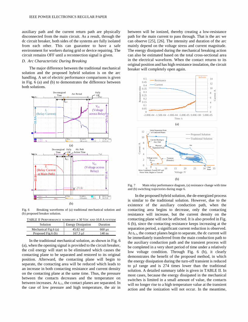
Fig. 7 Main relay performance diagram, (a) resistance change with time
and (b) switching trajectories during stage 6.
In the proposed hybrid solution, the de-energized process
is similar to the traditional solution. However, due to the
existence of the auxiliary conduction path, when the
contacting area begins to decrease, only the contacting
resistance will increase, but the current density on the
contacting plane will not be affected. It is also proofed in Fig.
6 (b), since the contacting resistance keeps increasing at the
separation period, a significant current reduction is observed.
At t6.1, the contact planes begin to separate, the dc current will
be immediately transferred from the main conduction path to
the auxiliary conduction path and the transient process will
be completed in a very short period of time under a relatively
low voltage condition. Through Fig. 6 (b), it clearly
demonstrates the benefit of the proposed method, in which
the energy dissipation during the turn-off transient is reduced
to µJ range and is 274 times lower than the traditional
solution. A detailed summary table is given in TABLE II. In
most cases, because the energy dissipated in the mechanical
switches is limited in a small amount of value, the contacts
will no longer rise to a high temperature value at the transient
action and the ionization will not occur. In the meantime,
I1
(Relay Current)
VR1
(Voltage
across Relay)
De-energized
TimeArc Period
Fully
Off
t6.1
30
Vdc
10.8
A
VR1
(Voltage across
Relay)
De-energized
Time
Alt. Path
Action Time
Fully
Off
t6.1
30
Vdc
10.8
A
I1
(Relay Current
at Main Path)
2Vdc
0
2
4
6
8
10
12
14
0
0.05
0.1
0.15
0.2
0.25
0.3
0.35
0.4
0.45
0.5
-2.00E-04 -1.50E-04 -1.00E-04 -5.00E-05 0.00E+00 5.00E-05
Curr
ent
/A
Time /s
Resistance
Current
Res
ista
nce
/ohm
Infinite
0
2
4
6
8
10
12
0 5 10 15 20 25 30 35
Cu
rren
t /A
Voltage /V
Proposed Solution
Traditional Solution
Initial Separation Point
of Contacted Planes
Physical
Separation Point
Transient
(Parasitic)
Current Sharing to
Aux. Path
Relay Completely Turned OFF and
Power Semi. Begins to Turn-off
Arc
Voltage across
RDS(ON)
End
Point

IEEE POWER ELECTRONICS REGULAR PAPER
according to Fig. 6, the corresponding resistivity over time
and the switching trajectories at the turn-off transient are
found and are given in Fig. 7(a) and (b), respectively. It
clearly showed that no ionized low conduction path had
resulted and the main relay was able to turn-off in a relative
LV range. Thus, the possibility of arcing is highly reduced
and a smoothly reopening is able to provide in each
mechanical switching action. By having an appropriate
circuit design, the energy dissipated in the mechanical switch
can be limited to a specific value that does not cause
ionization and arcing. Even in some unexpected situations,
the energy is higher than expected, and the mechanical relay
still has the ability to handle the arc at the specified power
rated of the relay, and will not cause any system failure. A
detailed switching diagram on the positive terminal is also
given in Fig. 8 to explain the current flow during the turn-off
transient.
Fig. 8 Equivalent circuit on positive terminal during turn-off transient.
III. SELECTION OF COMPOMENTS
The proposed circuit is a hybrid dc breaker solution,
which consists of both mechanical relays and semiconductor
devices. In a traditional dc breaker solution, a single
mechanical relay or a solid-state breaker is applied to act as
both power line current conductors during the normal
situation and circuit breaker during the transient situation.
Among the traditional breaker technologies, mechanical
relay and solid-state relay are two of the commonly used
devices. Some of the existing dc breakers on the markets are
listed in TABLE III as reference. The key features are
highlighted in the table. The mechanical relays are physical
switches, which use the electromagnetic contact to control the
circuit operation. They are with low conduction resistance
and can provide high-level insulation on the device. However
it is not able to handle the surge current and the durability is
usually poor, around 10 k times. In contrast, the solid-state
relays are most likely semiconductor-based. It provides fast
response and low contacting arc. The drawback is the high
conduction resistance and the absence of physical isolation.
Hence, for solid-state relays, the overall system reliability is
limited and the system efficiency is restricted.
Different from the single breaker solution, in the proposed
solution, the major functions in the dc breaker circuit solution
are separated clearly into two divisions, current conduction
and circuit breaking. Each function is handled by a certain
device, the advantage of both types of device can be fully
utilized while their disadvantages are eliminated in the hybrid
solution. In the design, mechanical relays are selected to
handle the current conduction in the power line during the
normal situation, and semiconductor switches are selected to
handle the breaking action during the transient period. The
target system parameter is highlighted in durability is
TABLE III.
A. Selection of Mechanical Relays
In the traditional approach, during each switching action,
an electrical arc will be generated between the two contacted
planes. One of the examples is given in Fig. 9 (a), which is
conducted under the on-site test. Under high voltage and high
current on-off actions, the resulting high energy electrical arc
R1
RAIA
I1 IO
SA2SA1
R1
RA
I1 IO
Normal Conduction Stage 5
RAIA
I1 IO
Beginning of Stage 6
SA2SA1
R1
RA
Stage 8
SA2SA1
RA
Stage 7
R1R1
RAIA
IO
End of Stage 6
RAIA
I1 IO
After t6.1
RDS
SA1 &SA2
R1
RDS
SA1 &SA2
R1
RDS
SA1 &SA2
RDS
SA1 &SA2
TABLE III SYSTEM PARAMETERS COMPARISON WITH COMMERCIAL PRODUCTS
Model Hongfa -HFS33/D-200D10M Crydom -84137850 TE Connectivity -AP10B245 Omron Electronics -G9EB-1 Proposed
Type SolidState SolidState Mechanical Vacuum Relay Mechanical with gas-filled Hybrid
DC Voltage /V 200 200 270 250 380
DC Current /A 10 10 10 20 15
Max Surge /A (10ms) 40 60 N.A N.A 80
Resistance / Ω 105m 210m 10m 30m < 5m
Electrical Durability > 100k > 100k 7k 30k > 100k
Dielectric Strength N.A N.A 2000 Vrms 2500 Vrms 1000 Vrms

IEEE POWER ELECTRONICS REGULAR PAPER
(a) (b)
Fig. 9 Experimental diagrams of mechanical relay (a) during electric arcs and (b) after repetitive switching action.
will heat the contacted plane and oxidize a small portion of
the surface in each time. For the oxidized area will result in
high resistive and influence the next performance. After a
long term repetitive breaking action, the surface will be
completely oxidized and the contactor may be bent, as shown
in Fig. 9 (b). As a result, the relay will no longer function
properly and result in failure.
In the proposed solution, mechanical relays are applied to
handle the current conduction in the power line during the
normal situation and to provide a physical isolation feature.
Thus, when selecting, both voltage and current ratings are
important parameters to be considered. The voltage rating of
the relay is used to support the breakdown voltage of the
ystem and the current rating of the relay is used to handle the
current capability during the conduction period. Meanwhile,
response time is another parameter in concern. In the
proposed solution, it targets for low voltage public grid
application. Thus, it is required that the selected relay has a
response time of ms.
As discussed in Section II, different from the traditional
approach, in the proposed solution, all the mechanical relays
are switched under low energy dissipation condition.
Therefore, in the proposed solution, the choice of relays
becomes more extensive, the design can consider:
1) The use of ac relays in a dc relay circuit. All the relays are
switched under either relatively LV or floating
conditions,which means that the electrical stress applied to
the components during the transient actions is at a relatively
low value and can be limited within the ac relay specified dc
switching voltage. The ac voltage rating of the relays is only
used to guarantee that the circuit with enough voltage
insulation for the system. Therefore, ac relays can be adopted
into the selection on the mechanical relays instead of the
bulky and expensive dc relays. For example, a 250Vac relay
can apply to a dc circuit breaker design up to 353.6 Vdc.
Therefore, it is especially suitable for LV dc MG.
2) Mechanical durability as relay durability instead of using
electrical durability. The main power relay R1 is always
paralleled with a low resistance path during the switching
transient. Thus, a smooth current transient is always
guaranteed in R1. The other two relays, RA and R2, are even
better which are switched under zero current situation. All the
relays are switched with low energy dissipation and the
possibility of the electrical arc becomes relatively small.
Accordingly, it provides an opportunity to extend the
electrical durability of the applied mechanical relays to a
value close to the mechanical durability defined in the
datasheet and result in a longer lifetime in the entire solution
compared to the traditional fully mechanical solution. The
extension of life time will be more dependent on the
maximum amount of energy dissipation in the mechanical
relays.
Overall, in the target 150/380 Vdc and 15A dc breaker
system, an ac relay, G2R-1A-E, is selected. It features with a
16A current capability, a maximum 380 Vac switching
voltage, 100 k times in mechanical durability, 2 mΩ low
resistance characteristic, and 7-9 ms mechanical action time.
Thus, it fits for the target power ratings and helps to produce
designs with high durability and high efficiency.
B. Selection of Semiconductors
In the design, semiconductor switches are applied to
handle the transient switching action in the breaker circuit. A
pair of semiconductor switches are required to apply at the
same time to produce the bidirectional blocking
characteristic. For discrete devices, they can be arranged into
a back-to-back, drain-to-drain, or other bidirectional
Electric
Arcs
TABLE IV Selected components in the prototype
Device Requirement Selection
Conduction Isolation Switching Model Type
R1 Power Line Yes Low Voltage G2R-1A-E AC Mechanical Relay
R2 Power Line Yes ZCS G2R-1A-E AC Mechanical Relay
RA Auxiliary Path Yes ZCS G2R-1A-E AC Mechanical Relay
SA Auxiliary Path No None IPW60R125C6 MOSFET

IEEE POWER ELECTRONICS REGULAR PAPER
configuration. In the selection, the voltage and current ratings
of the semiconductors are determined by the operating
voltage and the current capability of the system, respectively.
In addition, inrush current capability is another parameter to
consider in semiconductor selection. It is used to support the
system response during faults and is defined by the maximum
short circuit current and the worst-case energy information in
the system.
Fig. 10 MOSFET overvoltage performance at stage 7.
Among the switching sequences, the most critical
breaking action appears in stage 7. At stage 4 and stage 5, SA
is switched ON and OFF under relatively low voltage
conditions, respectively. However, at stage 7, due to the
presence of parasitic inductance in the loop, high voltage
stress will occur between the drain and source of the
semiconductor under the turn-off transient. The detailed
switching action of SA during stage 7 is given in Fig. 10.
A pair of protection diodes has been applied to the system,
generally, no overvoltage conditions will occur. However, for
IGBTs or other semiconductor devices that without
overvoltage capability, a parallel MOV is still recommended
to avoid any excessive transient voltages. Differently, power
MOSFET doesn’t have this requirement. Inside a traditional
MOSFET, there is a group of parasitic components inside the
physical structure, such as parasitic resistance in P-well
channel structure and a parasitic NPN bipolar transistor
structure [27]. Normally, the parasitic NPN is effectively
shorted. However, during the turn-off moment, a strong
electric field is resultant inside the device which causes
current flow proximity to the parasitic NPN transistor
internally. Once the current flow causes sufficient voltage
across on it, the parasitic bipolar transistor will become
activated and will claim the device voltage at a value that is
1.2 to 1.3 times higher than the general breakdown voltage.
Thus, power MOSFET can protect by the avalanche mode
during the worst-case scenario and more suitable for the LV
MG applications.
The worst-case energy is able to determine from the
circuit relationship at stage 7. By applying Kirchhoff’s
voltage law to the main current loop, the detail characteristic
of the overvoltage or the avalanche period can be determined.
The circuit relationship at stage 7 is formed as,
𝑉DD = 𝑉DS,Peak + 𝐿loop ∙𝑑𝐼(𝑡)
𝑑𝑡+ 𝑅loop ∙ 𝐼(𝑡), (1)
where VDD is dc voltage at the input side, VDS,Peak is
overvoltage or the avalanche voltage applied to the
semiconductor in stage 7, I is dc current flowing in the circuit,
Lloop is loop inductance or parasitic inductance in the current
path and Rloop is parasitic resistance at the current path.
By solving (1) with the start point and the endpoint circuit
information, the corresponding turn-off time, tOFF, is
determined as,
𝑡OFF =𝐿loop
𝑅loopln [1 +
𝐼peak∙𝑅loop
𝑉DS,Peak−𝑉DD]. (2)
During the turn-off period, the power dissipation in the
MOSFET is approximating to a triangle waveform.
According, the corresponding energy dissipation, EOFF, is
simplified to,
𝐸OFF ≅1
2∙ 𝑉DS,Peak ∙ 𝐼peak ∙
𝐿loop
𝑅loopln [1 +
𝐼peak∙𝑅loop
𝑉DS,Peak−𝑉DD]. (3)
With the use of (3), the maximum rating in the target
system and a 2 µH parasitic loop inductance as the worst case
assumption, a 0.2 mJ worst-case energy dissipation can be
calculated.
According to the maximum rating of the target system,
150/380 Vdc and 15 A, the worst-case energy dissipation, 0.2
mJ, and a five-time short circuit capability, 75 A, in the target
dc breaker system, a discrete TO247 power MOSFET,
IPW60R125C6, is selection. It features with a 0.96 mJ for
repetitive energy, around 89 A pulse current at 25 ̊C, and
with a 600 Vdc breakdown. A summary of the selected
components is given in TABLE IV.
IV. EXPERIMENTAL VERIFICATIONS
A 150/380 Vdc and 15 A test platform with a dc breaker
prototype, as shown in Fig. 11, is built to verify the
performance of the proposed dc circuit breaker and the target
operating conditions defined in TABLE I. The prototype
shows that the entire system is controlled by a single
microcontroller and the protection feature comes from the
accurate current detection by the Hall-effect sensors.
Compared to the two relays traditional system, in the
proposed solution, an extra relay and a pair of semiconductor
switches were applied, in which the semiconductor pair were
arranged in back-to-back connection. According to the given
control strategy, the power consumption of the auxiliary
circuit was kept within 3 W. At the standby mode, only 0.95
W was consumed. At the normal operation mode, 2.85 W was
consumed, which is closed to the traditional approach.
SA
t7-0 t7-1tOFF
VSA
IA
VDD
VDS,Peak
PSA
Tj
Tamb

IEEE POWER ELECTRONICS REGULAR PAPER
(a)
(b)
Fig. 11 Hardware diagrams of (a) test setup and (b) dc circuit breaker
prototype.
In Fig. 12, it demonstrates a complete operating sequence
of the proposed circuit during on and off conditions under a
10 Ω resistive load and 150Vdc input. The resultant
operational sequence was the same as the one proposed in
Section II. Each transient operation, it was able to divide into
two parts, the electrical operation process, TON,SW and
TOFF,SW, and the physical setting process, TON,SET and TOFF,SET.
In both actions, their durations are also highly dependent on
the response time of mechanical relays, which are about 7 to
9 ms. For example, in Fig. 12 (a), after the turn-on signal
provides to R1 at t1, it takes 8 ms to settle, and then the
semiconductors respond in another few hundred ns and
complete the electrical operation process. A similar situation
appeared in the physical setting process. Overall, the
electrical transient action was able to complete in 8 ms, which
fulfills with requirement protect feature in dc MGs of fault
current interruption within 0.01 s [28], [29], and is
compatible with other mechanical-based LVDC hybrid
circuit breaker solutions and mechanical solutions in ms
response time [20], [29]. Together with the physical isolation
action, the overall required start-up time was around 23 ms
and the overall turn-off action was within 16 ms. The slight
difference in the switching transient time, it comes from the
charging and discharging characteristic of RA. In the turn-on
period, the energy comes from an auxiliary power, thus, the
maximum supplying power is limited and it causes a longer
time in charging. In the turn-on period, the energy comes
from an auxiliary power, thus, the coil power is released
through a freewheeling diode and a compensation resistor,
thus, a fast discharging time is resultant.
In Fig. 12 (a), it shows the switching pattern that relates
to the physical setting process, where R2 and RA are
synchronized in action. During this processing period, the
system did not have any power flow and operated at ZCS. It
either worked to establish a system connection path at t1
before the current flow began or produce the physical
isolation at t8 after the current return path was disconnected.
In Fig. 12 (b), it shows the switching pattern that relates to
the electrical operation process. SA was only active during the
switching transient at the dc breaker circuit. It provided an
auxiliary path for the current conduction during the transient
period. R1 was only switched when SA was active. Thus, it
always operated with a parallel auxiliary path during the on-
off action. A smoothly current transient waveform was
observed in waveform and no electrical arc was visually
observed from the experimental setup.
Under the purely resistive loading, the turn-on and turn-
off switching performances of the semiconductor pair at the
150 Vdc system are shown in Fig. 13 (a) and (b), respectively.
In both cases, the switching time was also maintained within
1 μs. It proved that the major restriction in the operation time
of the hybrid circuit was mainly limited by the mechanical
operation. If a faster system response is required, an ultra-fast
mechanical ac relay can be considered in R1 and the rest of
the circuit does not affect. But there is a trade-off of cost and
response time. Also, from Fig. 13, it demonstrates that the
semiconductor pair is able to handle the transient responses
in the dc breaker circuit properly and no over voltage scenario
happens. Thus, a safe response was still able to be guaranteed.
For the designed platform, the maximum safety voltage
capability is 380 Vdc. Under this condition, stable
performance is able to guaranteed and is demonstrated in Fig.
14. In Fig. 14 (a), it shows a complete operating cycle of the
proposed solution at 380 Vdc operating voltage, where the
operation remains the same as in the 150 Vdc test case. Also,
as shown in Fig. 14 (b), a fast semiconductor action is
provided by SA and no overvoltage scenario happens. Overall,
the electrical operation time maintained within 8 ms and no
electrical arc visually observed.
In Fig. 15, the platform serves with the same working
condition as Fig. 14, where the only difference was the
protection diode is eliminated in the test. Even a purely
resistive load is connected, during the turn-off time period,
the overvoltage situation was still easily triggered by the
parasitic inductance and caused electrical stress to the
semiconductors. Thus, it was important to have the protection
diode in the design.
In order to verify the reliability and the bidirectional
capability of the platform, a group of performance test has
been done and is shown in Fig. 16 and Fig. 17, respectively.
In Fig. 16, repeated interrupts are performed on the designed
system. The test sequence is given with 200 ms per cycle at
150 Vdc and 15 A. Two sets of circuit prototypes were tested.
Both of them were capable of running cycles above 100
thousand times, which was much higher than the traditional

IEEE POWER ELECTRONICS REGULAR PAPER
mechanical solution shown in TABLE III. Thus, the high
durability performance of the proposed solution is
experimentally verified. In Fig. 17, a reverse conduction
situation is demonstrated, in which the current direction is
opposite to the test result in Fig. 12. Under the same circuit
settings, it shows the same performance in both current
directions. Thus, it proofed that the system was able to
achieve stable performance in bidirectional current flow.
Apart from the normal shutdown operation, the system
also performed stable under fault scenarios. In Fig. 18, it
demonstrates the system performance at an over current
scenario. In the evaluation, an inductive load was applied,
which was formed by a 20 mH grid inductor and a 12.5 Ω
electronic load. To perform the over current assessment, load
transient was applied to result in an over-specified current to
appear and the system would trigger when the current
exceeded the limit of 15 A. In Fig. 18 (a), the output load was
dropped from 12.5 Ω to 3 Ω and the system successfully
disconnects both terminal connections at an overrating
current, 48 A. Similarly, In Fig. 18 (b), the output load was
dropped from 12.5 Ω to 1.67 Ω and the system successfully
disconnects both terminals connection at an overrating
current, 78 A. In both cases, the electrical switching time was
maintained within 8 ms, low energy dissipation in all those
relays, no electrical arcs were visually observed, and a correct
semiconductor breaking waveform was observed.
Meanwhile, the inductive energy was handled well by
the protection diode after the circuit breaker was opened. All
the performance was kept the same as the normal operation.
Overall, a stable protection system was guaranteed.
(a) (b)
Fig. 12 Experimental results under purely resistive loading that relates to (a) circuit isolation feature and (b) current conduction channel.
(a) (b)
Fig. 13 Experimental results of SA under purely resistive loading at 150 Vdc 15A system, (a) turn-on transient at t2 and (b) turn-off transient at t7.
(a) (b)
Fig. 14 Experimental results under purely resistive load at 380 Vdc 15A system, (a) full cycle switching performance and (b) turn-off transient of SA at t7.
t1 t2 t7 t8
IO
VDD
Signal of RA & R2
VR1
TON,SET Conduction Period TOFF,SetPhyscial
Isolated
t2 t4 t7t5
IO
IA
Signal
of SA
Signal
of R1
TON,SW Normal Operation PeriodElectrical
IsolatedTOFF,SW
~ 8ms
IO
IA
VDS,SA
VGS,SA
150Vdc
IO
IA
VDS,SA
VGS,SA
150Vdc
265Vdc
t2 t4 t7t5
IO
IA
VDD,A
VDD,B
TON,SW Normal Conduction PeriodElectrical
IsolatedTOFF,SW
~ 7.5ms15A
380Vdc
IO
IA
VDS,SA
VGS,SA
380Vdc
475Vdc

IEEE POWER ELECTRONICS REGULAR PAPER
Fig. 15 Turn-off transient result of SA in without diode protection situation.
Fig. 16 Reliability testing sequence under pure resistive load.
Fig. 17 Experimental result under reverse current flow.
(a) (b)
Fig. 18 Experimental results of overcurrent protection under inductive load, (a) breaking at 48A and (b) breaking at 78A.
V. CONCLUSION
The paper presented an alternative solution to the dc
breaker design. In the concept, it makes use of both
mechanical switches and semiconductor switches. Each of
them deals with a key feature in the dc breaker. The
mechanical switches focus on the normal conduction and the
semiconductor switches handle the breaker transient.
Therefore, the breaker design guarantees with bidirectional
current flow, galvanic isolation, high reliability, and high
efficiency for low voltage dc applications. The performance
of the proposed concept was experimentally verified in a 250
V, 15A dc breaker setup, where the operation of both resistive
and inductive loads have been tested. The results showed that
the proposed solution achieved a fast response in switching
action and was featured with high-reliability performance.
All the demonstration results are shown with a good
agreement is achieved between theoretical concepts and
experimental results. The proposed dc hybrid breaker is
promising for the applications of LV dc grid, PV array, and
battery protection.
REFERENCE
[1] Accetta and M. Pucci, “Energy Management System in DC Micro-
Grids of Smart Ships: Main Gen-Set Fuel Consumption Minimization and Fault Compensation,” IEEE Trans. Ind. Appl.,
vol. 55, no. 3, pp. 3097-3113, May-Jun. 2019.
[2] Z. Jin, L. Meng, J. M. Guerrero, and R. Han, “Hierarchical Control Design for a Shipboard Power System With DC Distribution and
Energy Storage Aboard Future More-Electric Ships,” IEEE Trans.
Ind. Informat., vol. 14, no. 2, pp. 703-714, Feb. 2018. [3] P. Sanjeev, N. P. Padhy, and P. Agarwal, “Peak Energy
Management Using Renewable Integrated DC Microgrid,” IEEE
Trans. Smart Grid, vol. 9, no. 5, pp. 4906-4917, Sept. 2018.
IO
IA
VDS,SA
VGS,SA
380Vdc
720Vdc
~ 200ms
IO
IA
VDD,A
VDD,Bt4 t5 t7t2
IO
IA
VDD,A
VDD,B
TON,SW Normal Operation PeriodElectrical
IsolatedTOFF,SW
~ 8ms
- 15A
150Vdc
t7t5
IO
IA
VDD,A
Signal of SA
15 A
48 A
Over Current
Point
Electrical
Isolated
TOFF,SW
~7.8ms
t7t5
IO
IA
VDD,A
Signal of SA
15 A
78 A
Over Current
Point
Electrical
Isolated
TOFF,SW
~7.8ms

IEEE POWER ELECTRONICS REGULAR PAPER
[4] L. Roggia, L. Schuch, J. E. Baggio, C. Rech, and J. R. Pinheiro,
“Integrated Full-Bridge-Forward DC–DC Converter for a
Residential Microgrid Application,” IEEE Trans. Power Electron.,
vol. 28, no. 4, pp. 1728-1740, April 2013. [5] A. Chub, D. Vinnikov, R. Kosenko, L. Liivik, and I. Galkin,
“Bidirectional DC-DC Converter for Modular Residential Battery
Energy Storage Systems,” IEEE Trans. Ind. Electron., vol. 67, no. 3, pp. 1944-1955, Mar. 2020.
[6] “Power generation system and inverter for feeding power into a
three-phase grid”, US patent, US8779630B2, 2009. [7] “Method for checking a separation point of a photovoltaic inverter,
and photovoltaic inverter”, US patent, US9494659B2, 2012.
[8] “Detection of welded switch contacts in a line converter system”, US patent, US20110298470A1, 2011.
[9] Y. Kishida, K. Koyama, H. Sasao, N. Maruyama, and H. Yamamoto,
“Development of the high speed switch and its application,” Proc. IEEE Ind. Appl. Conf., Oct. 1998, pp. 2321–2328, vol. 3.
[10] J. Meyer and A. Rufer, “A DC hybrid circuit breaker with ultra-fast
contact opening and integrated gate-commutated thyristors
(IGCTs),” IEEE Trans. Power Del., vol. 21, no. 2, pp. 646-651, Apr.
2006.
[11] “A hybrid circuit breaker”, European Patent, EP2489053 (B1), 2009.
[12] C. Meyer, M. Kowal and R. W. De Doncker, “Circuit breaker
concepts for future high-power DC-applications,” Industry Applications Conference, vol. 2, pp. 860-866, Oct. 2005.
[13] J. Hafner and B. Jacobson, “Protective Hybrid HVdc Breakers - A Key Innovation for Reliable HVdc Grids,” CIGRE International
Symposium, Bologna, Sept. 2011.
[14] C. Peng, X. Song, A. Q. Huang, and I. Husain, “A Medium-Voltage Hybrid DC Circuit Breaker—Part II: Ultrafast Mechanical Switch,”
Trans. Emerg. Sel. Topics Power Electron., vol. 5, no. 1, pp. 289-
296, Mar. 2017. [15] X. Song, C. Peng and A. Q. Huang, “A Medium-Voltage Hybrid
DC Circuit Breaker, Part I: Solid-State Main Breaker Based on 15
kV SiC Emitter Turn-OFF Thyristor,” Trans. Emerg. Sel. Topics Power Electron., vol. 5, no. 1, pp. 278-288, Mar. 2017.
[16] C. Peng, A. Q. Huang, and X. Song, “Current commutation in a
medium voltage hybrid DC circuit breaker using 15 kV vacuum switch and SiC devices,” Proc. IEEE APEC, Mar. 2015, pp. 2244-
2250.
[17] “HVDC hybrid circuit breaker with snubber circuit,” US Patent, US8891209 (B2), 2011.
[18] “Hybrid dc circuit breaking device,” US Patent, US20150022928
(A1), 2012. [19] “High-voltage dc circuit breaker apparatus,” European Patent,
EP0108279 (B2), 1982.
[20] R. Lazzari and L. Piegari, “Design and Implementation of LVDC Hybrid Circuit Breaker,” IEEE Trans. Power Electron., vol. 34, no.
8, pp. 7369-7380, Aug. 2019.
[21] X. Pei, O. Cwikowski, A. C. Smith, and M. Barnes, “Design and Experimental Tests of a Superconducting Hybrid DC Circuit
Breaker,” in IEEE Trans. on Appl. Supercond., vol. 28, no. 3, pp. 1-
5, Apr. 2018. [22] “Commutation type DC breaker”, US Patent, US5452170A, 1992.
[23] D. Jovcic, “Series LC DC circuit breaker”, IET High Voltage, vol,
4, iss. 2, pp. 130- 137, Jul. 2019.
[24] “Device and method for switching a direct current,” US Patent,
US20160300671 (A1), 2013.
[25] R. Ma et al., “Investigation on Arc Behavior During Arc Motion in Air DC Circuit Breaker,” IEEE Trans. on Plasma Sci., vol. 41, no.
9, pp. 2551-2560, Sept. 2013.
[26] Y. Kim and H. Kim, “Modeling for Series Arc of DC Circuit Breaker,” IEEE Trans. Ind. Appl., vol. 55, no. 2, pp. 1202-1207,
Mar. - Apr. 2019.
[27] T. McDonald, M. Soldano, A. Murray, and T. Avram, “Power MOSFET Avalanche Design Guidelines,” International Rectifier
Application Note, AN-1005, Oct. 2004.
[28] J. S. Morton, “Circuit Breaker and Protection Requirements for DC
Switchgear used in Rapid Transit Systems,” IEEE Trans. Ind. Appl.,
vol. IA-21, no. 5, pp. 1268-1273, Sept. 1985.
[29] D. Salomonsson, L. Soder, and A. Sannino, “Protection of Low-Voltage DC Microgrids,” IEEE Trans. Power Del., vol. 24, no. 3,
pp. 1045-1053, Jul. 2009.
[30] S. Beheshtaein, R. Cuzner, M. Savaghebi, and J. M. Guerrero, “Review on microgrids protection,” IET Generation, Transmission
& Distribution, vol. 13, no. 6, pp. 743-759, Mar. 2019.