DE0-Nano-SoC Computer System with Nios...
36
DE0-Nano-SoC Computer System with Nios II For Quartus Prime 16.1 1 Introduction This document describes a computer system that can be implemented on the Intel DE0-Nano-SoC development and education board. This system, called the DE0-Nano-SoC Computer, is intended to be used as a platform for experiments in computer organization and embedded systems. To support these beginning experiments, the system contains a processor, memory, an analog-to-digital converter, an accelerometer and some simple I/O peripherals. The FPGA programming file that implements this system, as well as its design source files, can be obtained from the University Program section of Intel’s web site. 2 DE0-Nano-SoC Computer Contents As indicated in the figure, the components in this system are implemented utilizing both the FPGA and the Hard Processor System (HPS) inside Intel’s Cyclone R V SoC chip. The FPGA implements two Nios II processors and several peripheral ports: memory, timer modules, analog-to-digital, and parallel ports connected to switches and lights. The HPS comprises an ARM Cortex A9 dual-core processor and a set of peripheral devices. Instructions for using the HPS and ARM processor are provided in a separate document, called DE0-Nano-SoC Computer System with ARM Cortex-A9. 2.1 FPGA Components As shown in Figure 1 many of the components in the DE0-Nano-SoC Computer are implemented inside the FPGA in the Cyclone V SoC chip, as described below. 2.2 Nios II Processor The Intel Nios R II processor is a 32-bit CPU that can be implemented in an Intel FPGA device. Three versions of the Nios II processor are available, designated economy (/e), standard (/s), and fast (/f). The DE0-Nano-SoC Computer includes two Nios II processors, both of which are the fast version. An overview of the Nios II processor can be found in the document Introduction to the Intel Nios II Processor, which is provided in the University Program’s web site. An easy way to begin working with the DE0-Nano-SoC Computer and the Nios II processor is to make use of a utility called the Intel FPGA Monitor Program. It provides an easy way to assemble/compile Nios II programs written in either assembly language or the C language. The Monitor Program, which can be downloaded from Intel’s web site, is an application program that runs on the host computer connected to the DE0-Nano-SoC board. The Monitor Program can be used to control the execution of code on Nios II, list (and edit) the contents of processor registers, display/edit the contents of memory on the DE0-Nano-SoC board, and Intel Corporation - FPGA University Program November 2016 1
Transcript of DE0-Nano-SoC Computer System with Nios...
DE0-Nano-SoC Computer Systemwith Nios II
For Quartus Prime 16.1
1 Introduction
This document describes a computer system that can be implemented on the Intel DE0-Nano-SoC developmentand education board. This system, called the DE0-Nano-SoC Computer, is intended to be used as a platform forexperiments in computer organization and embedded systems. To support these beginning experiments, the systemcontains a processor, memory, an analog-to-digital converter, an accelerometer and some simple I/O peripherals.The FPGA programming file that implements this system, as well as its design source files, can be obtained fromthe University Program section of Intel’s web site.
2 DE0-Nano-SoC Computer Contents
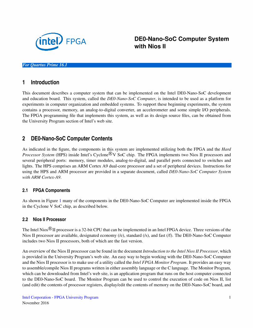
As indicated in the figure, the components in this system are implemented utilizing both the FPGA and the HardProcessor System (HPS) inside Intel’s Cyclone R©V SoC chip. The FPGA implements two Nios II processors andseveral peripheral ports: memory, timer modules, analog-to-digital, and parallel ports connected to switches andlights. The HPS comprises an ARM Cortex A9 dual-core processor and a set of peripheral devices. Instructions forusing the HPS and ARM processor are provided in a separate document, called DE0-Nano-SoC Computer Systemwith ARM Cortex-A9.
2.1 FPGA Components
As shown in Figure 1 many of the components in the DE0-Nano-SoC Computer are implemented inside the FPGAin the Cyclone V SoC chip, as described below.
2.2 Nios II Processor
The Intel Nios R©II processor is a 32-bit CPU that can be implemented in an Intel FPGA device. Three versions of theNios II processor are available, designated economy (/e), standard (/s), and fast (/f). The DE0-Nano-SoC Computerincludes two Nios II processors, both of which are the fast version.
An overview of the Nios II processor can be found in the document Introduction to the Intel Nios II Processor, whichis provided in the University Program’s web site. An easy way to begin working with the DE0-Nano-SoC Computerand the Nios II processor is to make use of a utility called the Intel FPGA Monitor Program. It provides an easy wayto assemble/compile Nios II programs written in either assembly language or the C language. The Monitor Program,which can be downloaded from Intel’s web site, is an application program that runs on the host computer connectedto the DE0-Nano-SoC board. The Monitor Program can be used to control the execution of code on Nios II, list(and edit) the contents of processor registers, display/edit the contents of memory on the DE0-Nano-SoC board, and
Intel Corporation - FPGA University ProgramNovember 2016
1
DE0-NANO-SOC COMPUTER SYSTEM WITH NIOS II For Quartus Prime 16.1
Expansionports
Cyclone VFPGA
Timers
SW3-0LEDG7-0
Parallelports
Parallelports
KEY1-0
On-chipmemory
Host computer
USBBlasterPeripherals
DE0-Nano-SoC
DDR3port
DDR3chips
JTAGports
Parallelports
ARM
MPCore
Cortex A9
TimersCyclone VHPS
Ports
. . .
Board
Nios II
FPGA Bridges
LEDG
Port
KEY ADC
Port
(2)
G-Sensor
Port
Parallelports
Arduinoport
Figure 1. Block diagram of the DE0-Nano-SoC Computer.
similar operations. The Monitor Program includes the DE0-Nano-SoC Computer as a predesigned system that canbe downloaded onto the DE0-Nano-SoC board, as well as several sample programs in assembly language and Cthat show how to use the DE0-Nano-SoC Computer’s peripherals. Some images that show how the DE0-Nano-SoCComputer is integrated with the Monitor Program are described in Section 10. An overview of the Monitor Programis available in the document Intel FPGA Monitor Program Tutorial, which is provided in the University Programweb site.
All of the I/O peripherals in the DE0-Nano-SoC Computer are accessible by the processor as memory mappeddevices, using the address ranges that are given in the following subsections.
2 Intel Corporation - FPGA University ProgramNovember 2016
DE0-NANO-SOC COMPUTER SYSTEM WITH NIOS II For Quartus Prime 16.1
2.3 Memory Components
The DE0-Nano-SoC Computer has a DDR3 port, as well as three memory modules implemented using the on-chipmemory inside the FPGA. These memories are described below.
2.3.1 DDR3 Memory
The DE0-Nano-SoC Computer includes a 1 GB DDR3 memory that is connected to the HPS part of the Cyclone VSoC chip. The memory is organized as 256M x 32-bits, and is accessible using word accesses (32 bits), halfwords,and bytes. The Nios II processor can access the DDR3 memory through the FPGA bridge, using the addresses space0x40000000 to 0x7FFFFFFF.
2.3.2 On-Chip Memory
The DE0-Nano-SoC Computer includes a 32-Kbyte memory that is implemented inside the FPGA. This memory isorganized as 8K x 32 bits. This memory is accessible by both Nios II processors using addresses 0x08000000 to0x08007FFF.
2.3.3 On-Chip Memories
The DE0-Nano-SoC Computer includes two additional 32-Kbyte memories that are implemented in the Cyclone IVFPGA chip. Each of these memories is organized as 8K x 32 bits, and can be accessed using either word, halfword,or byte operations. Each Nios II processor is connected to only one of these memories and can access the memoryin the address range 0x00000000 to 0x00007FFF. Each Nios II processor uses this memory to access its reset andexception code, as well as other code or data.
2.3.4 Parallel Ports
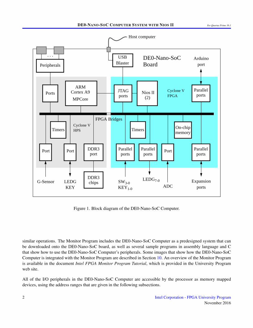
There are several parallel ports implemented in the FPGA that support input, output, and bidirectional transfers ofdata between the Nios II processor and I/O peripherals. As illustrated in Figure 2, each parallel port is assigneda Base address and contains up to four 32-bit registers. Ports that have output capability include a writable Dataregister, and ports with input capability have a readable Data register. Bidirectional parallel ports also include aDirection register that has the same bit-width as the Data register. Each bit in the Data register can be configuredas an input by setting the corresponding bit in the Direction register to 0, or as an output by setting this bit positionto 1. The Direction register is assigned the address Base + 4.
Some of the parallel ports in the DE0-Nano-SoC Computer have registers at addresses Base + 8 and Base + C, asindicated in Figure 2. These registers are discussed in Section 3.
2.3.5 Green LED Parallel Port
The green lights LED7−0 on the DE0-Nano-SoC board are driven by an output parallel port, as illustrated in Figure 3.The port contains an 8-bit Data register, which has the address 0xFF200000. This register can be written or readby the processor using word accesses, and the upper bits not used in the registers are ignored.
Intel Corporation - FPGA University ProgramNovember 2016
3
DE0-NANO-SOC COMPUTER SYSTEM WITH NIOS II For Quartus Prime 16.1
Address 02 14 331 30 . . .
Base
Base + 8
Base + C
Base + 4
Input or output data bits
Direction bits
Edge bits
Mask bits
Data register
Direction register
Interruptmask register
Edgecapture register
Direction bits
Figure 2. Parallel port registers in the DE0-Nano-SoC Computer.
0xFF200000
LED0LED7
Address
031 78 . . .Unused Data register
Figure 3. Output parallel port for LED.
2.3.6 Slider Switch Parallel Port
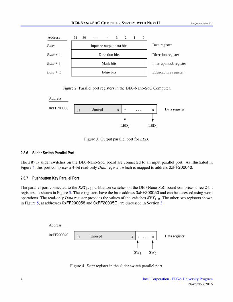
The SW3−0 slider switches on the DE0-Nano-SoC board are connected to an input parallel port. As illustrated inFigure 4, this port comprises a 4-bit read-only Data register, which is mapped to address 0xFF200040.
2.3.7 Pushbutton Key Parallel Port
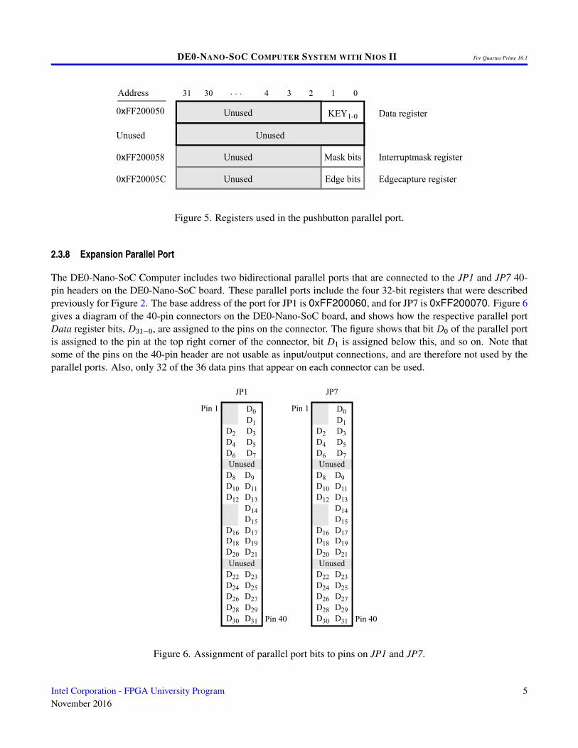
The parallel port connected to the KEY1−0 pushbutton switches on the DE0-Nano-SoC board comprises three 2-bitregisters, as shown in Figure 5. These registers have the base address 0xFF200050 and can be accessed using wordoperations. The read-only Data register provides the values of the switches KEY1−0. The other two registers shownin Figure 5, at addresses 0xFF200058 and 0xFF20005C, are discussed in Section 3.
0xFF200040
SW0SW3
Address
Data register031 34 . . .Unused
Figure 4. Data register in the slider switch parallel port.
4 Intel Corporation - FPGA University ProgramNovember 2016
DE0-NANO-SOC COMPUTER SYSTEM WITH NIOS II For Quartus Prime 16.1
Address 02 14 331 30 . . .
0xFF200050
0xFF200058
0xFF20005C
Unused
KEY1-0
Edge bits
Mask bits
Unused
Unused
Unused
Data register
Interruptmask register
Edgecapture register
Unused
Figure 5. Registers used in the pushbutton parallel port.
2.3.8 Expansion Parallel Port
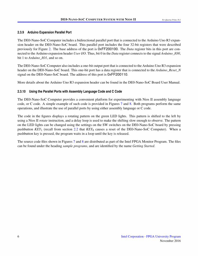
The DE0-Nano-SoC Computer includes two bidirectional parallel ports that are connected to the JP1 and JP7 40-pin headers on the DE0-Nano-SoC board. These parallel ports include the four 32-bit registers that were describedpreviously for Figure 2. The base address of the port for JP1 is 0xFF200060, and for JP7 is 0xFF200070. Figure 6gives a diagram of the 40-pin connectors on the DE0-Nano-SoC board, and shows how the respective parallel portData register bits, D31−0, are assigned to the pins on the connector. The figure shows that bit D0 of the parallel portis assigned to the pin at the top right corner of the connector, bit D1 is assigned below this, and so on. Note thatsome of the pins on the 40-pin header are not usable as input/output connections, and are therefore not used by theparallel ports. Also, only 32 of the 36 data pins that appear on each connector can be used.
D0D1
D2 D3D4 D5D6 D7Unused
D10 D11D12 D13
D14D15
D16 D17D18 D19
D22 D23D24 D25D26 D27D28 D29D30 D31
Unused
JP1 JP7
Pin 1 Pin 1
Pin 40 Pin 40
D8 D9
D20 D21
D0D1
D2 D3D4 D5D6 D7Unused
D10 D11D12 D13
D14D15
D16 D17D18 D19
D22 D23D24 D25D26 D27D28 D29D30 D31
Unused
D8 D9
D20 D21
Figure 6. Assignment of parallel port bits to pins on JP1 and JP7.
Intel Corporation - FPGA University ProgramNovember 2016
5
DE0-NANO-SOC COMPUTER SYSTEM WITH NIOS II For Quartus Prime 16.1
2.3.9 Arduino Expansion Parallel Port
The DE0-Nano-SoC Computer includes a bidirectional parallel port that is connected to the Arduino Uno R3 expan-sion header on the DE0-Nano-SoC board. This parallel port includes the four 32-bit registers that were describedpreviously for Figure 2. The base address of the port is 0xFF200100. The Data register bits in this port are con-nected to the Arduino expansion header User I/O. Thus, bit 0 in the Data register connects to the signal Arduino_IO0,bit 1 to Arduino_IO1, and so on.
The DE0-Nano-SoC Computer also includes a one-bit output port that is connected to the Arduino Uno R3 expansionheader on the DE0-Nano-SoC board. This one-bit port has a data register that is connected to the Arduino_Reset_Nsignal on the DE0-Nano-SoC board. The address of this port is 0xFF200110.
More details about the Arduino Uno R3 expansion header can be found in the DE0-Nano-SoC Board User Manual.
2.3.10 Using the Parallel Ports with Assembly Language Code and C Code
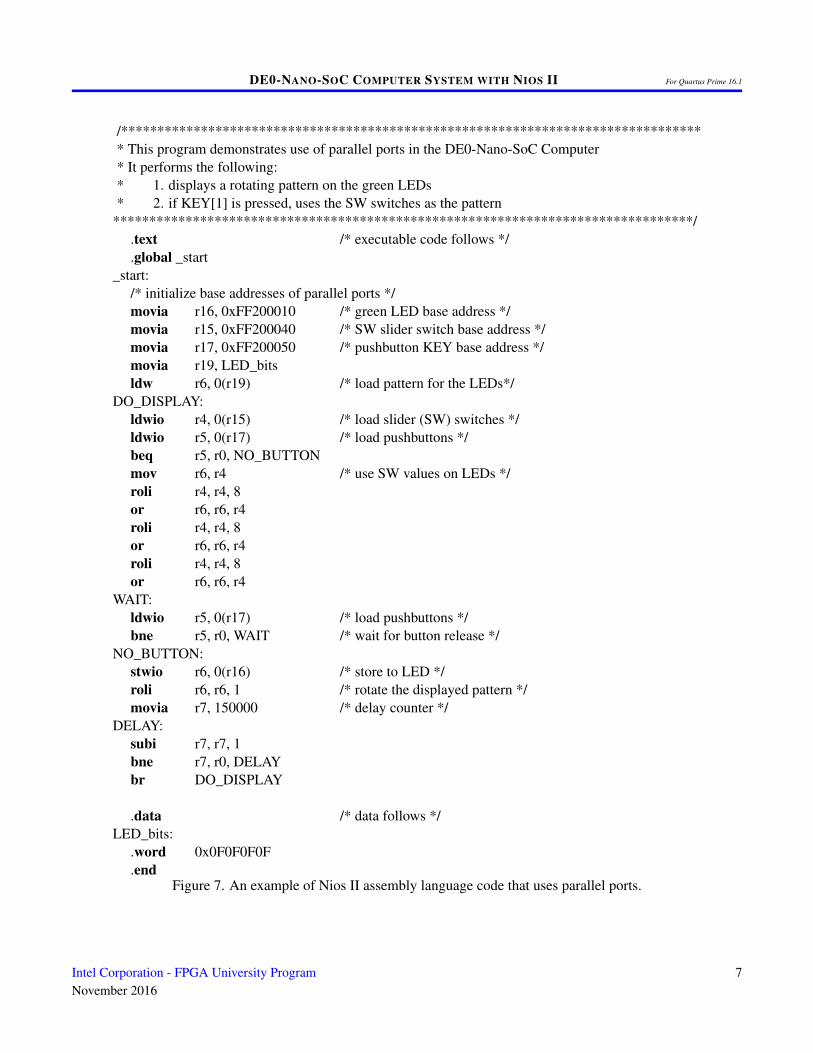
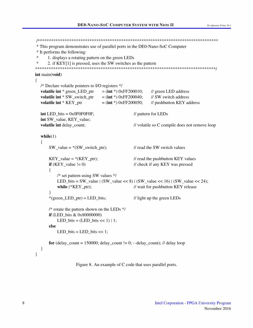
The DE0-Nano-SoC Computer provides a convenient platform for experimenting with Nios II assembly languagecode, or C code. A simple example of such code is provided in Figures 7 and 8. Both programs perform the sameoperations, and illustrate the use of parallel ports by using either assembly language or C code.
The code in the figures displays a rotating pattern on the green LED lights. This pattern is shifted to the left byusing a Nios II rotate instruction, and a delay loop is used to make the shifting slow enough to observe. The patternon the LED lights can be changed using the settings on the SW switches on the DE0-Nano-SoC board by pressingpushbutton KEY1 (recall from section 2.2 that KEY0 causes a reset of the DE0-Nano-SoC Computer). When apushbutton key is pressed, the program waits in a loop until the key is released.
The source code files shown in Figures 7 and 8 are distributed as part of the Intel FPGA Monitor Program. The filescan be found under the heading sample programs, and are identified by the name Getting Started.
6 Intel Corporation - FPGA University ProgramNovember 2016
DE0-NANO-SOC COMPUTER SYSTEM WITH NIOS II For Quartus Prime 16.1
/********************************************************************************* This program demonstrates use of parallel ports in the DE0-Nano-SoC Computer* It performs the following:* 1. displays a rotating pattern on the green LEDs* 2. if KEY[1] is pressed, uses the SW switches as the pattern
********************************************************************************/.text /* executable code follows */.global _start
_start:/* initialize base addresses of parallel ports */movia r16, 0xFF200010 /* green LED base address */movia r15, 0xFF200040 /* SW slider switch base address */movia r17, 0xFF200050 /* pushbutton KEY base address */movia r19, LED_bitsldw r6, 0(r19) /* load pattern for the LEDs*/
DO_DISPLAY:ldwio r4, 0(r15) /* load slider (SW) switches */ldwio r5, 0(r17) /* load pushbuttons */beq r5, r0, NO_BUTTONmov r6, r4 /* use SW values on LEDs */roli r4, r4, 8or r6, r6, r4roli r4, r4, 8or r6, r6, r4roli r4, r4, 8or r6, r6, r4
WAIT:ldwio r5, 0(r17) /* load pushbuttons */bne r5, r0, WAIT /* wait for button release */
NO_BUTTON:stwio r6, 0(r16) /* store to LED */roli r6, r6, 1 /* rotate the displayed pattern */movia r7, 150000 /* delay counter */
DELAY:subi r7, r7, 1bne r7, r0, DELAYbr DO_DISPLAY
.data /* data follows */LED_bits:
.word 0x0F0F0F0F
.endFigure 7. An example of Nios II assembly language code that uses parallel ports.
Intel Corporation - FPGA University ProgramNovember 2016
7
DE0-NANO-SOC COMPUTER SYSTEM WITH NIOS II For Quartus Prime 16.1
/********************************************************************************* This program demonstrates use of parallel ports in the DE0-Nano-SoC Computer* It performs the following:* 1. displays a rotating pattern on the green LEDs* 2. if KEY[1] is pressed, uses the SW switches as the pattern
********************************************************************************/int main(void){
/* Declare volatile pointers to I/O registers */volatile int * green_LED_ptr = (int *) 0xFF200010; // green LED addressvolatile int * SW_switch_ptr = (int *) 0xFF200040; // SW switch addressvolatile int * KEY_ptr = (int *) 0xFF200050; // pushbutton KEY address
int LED_bits = 0x0F0F0F0F; // pattern for LEDsint SW_value, KEY_value;volatile int delay_count; // volatile so C compile does not remove loop
while(1){
SW_value = *(SW_switch_ptr); // read the SW switch values
KEY_value = *(KEY_ptr); // read the pushbutton KEY valuesif (KEY_value != 0) // check if any KEY was pressed{
/* set pattern using SW values */LED_bits = SW_value | (SW_value << 8) | (SW_value << 16) | (SW_value << 24);while (*KEY_ptr); // wait for pushbutton KEY release
}*(green_LED_ptr) = LED_bits; // light up the green LEDs
/* rotate the pattern shown on the LEDs */if (LED_bits & 0x80000000)
LED_bits = (LED_bits << 1) | 1;else
LED_bits = LED_bits << 1;
for (delay_count = 150000; delay_count != 0; --delay_count); // delay loop}
}
Figure 8. An example of C code that uses parallel ports.
8 Intel Corporation - FPGA University ProgramNovember 2016
DE0-NANO-SOC COMPUTER SYSTEM WITH NIOS II For Quartus Prime 16.1
2.4 JTAG Port
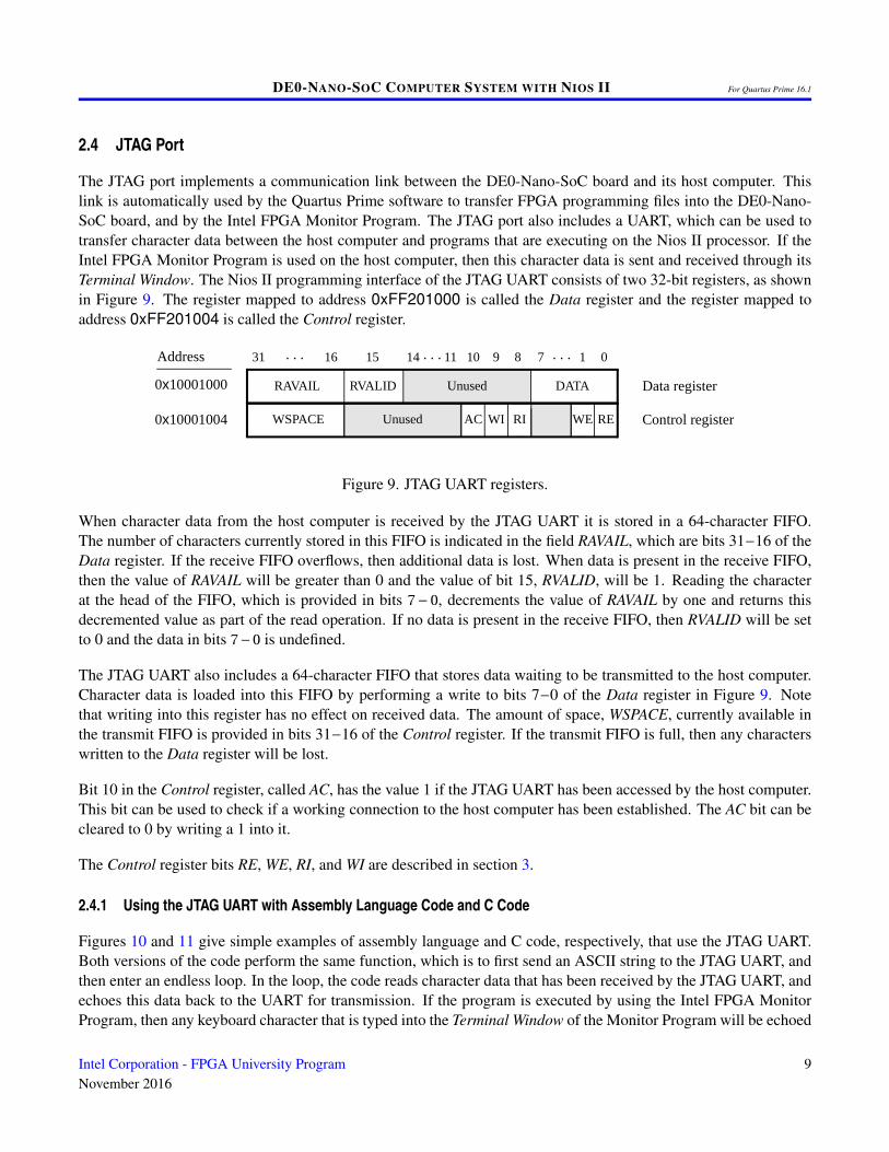
The JTAG port implements a communication link between the DE0-Nano-SoC board and its host computer. Thislink is automatically used by the Quartus Prime software to transfer FPGA programming files into the DE0-Nano-SoC board, and by the Intel FPGA Monitor Program. The JTAG port also includes a UART, which can be used totransfer character data between the host computer and programs that are executing on the Nios II processor. If theIntel FPGA Monitor Program is used on the host computer, then this character data is sent and received through itsTerminal Window. The Nios II programming interface of the JTAG UART consists of two 32-bit registers, as shownin Figure 9. The register mapped to address 0xFF201000 is called the Data register and the register mapped toaddress 0xFF201004 is called the Control register.
Address 0731 16. . .
0x10001000
0x10001004
DATARAVAIL
14 8. . . . . .
WSPACE Unused WI RI WE RE
1
RVALID
AC
10 911
Unused
15
Data register
Control register
Figure 9. JTAG UART registers.
When character data from the host computer is received by the JTAG UART it is stored in a 64-character FIFO.The number of characters currently stored in this FIFO is indicated in the field RAVAIL, which are bits 31−16 of theData register. If the receive FIFO overflows, then additional data is lost. When data is present in the receive FIFO,then the value of RAVAIL will be greater than 0 and the value of bit 15, RVALID, will be 1. Reading the characterat the head of the FIFO, which is provided in bits 7−0, decrements the value of RAVAIL by one and returns thisdecremented value as part of the read operation. If no data is present in the receive FIFO, then RVALID will be setto 0 and the data in bits 7−0 is undefined.
The JTAG UART also includes a 64-character FIFO that stores data waiting to be transmitted to the host computer.Character data is loaded into this FIFO by performing a write to bits 7−0 of the Data register in Figure 9. Notethat writing into this register has no effect on received data. The amount of space, WSPACE, currently available inthe transmit FIFO is provided in bits 31−16 of the Control register. If the transmit FIFO is full, then any characterswritten to the Data register will be lost.
Bit 10 in the Control register, called AC, has the value 1 if the JTAG UART has been accessed by the host computer.This bit can be used to check if a working connection to the host computer has been established. The AC bit can becleared to 0 by writing a 1 into it.
The Control register bits RE, WE, RI, and WI are described in section 3.
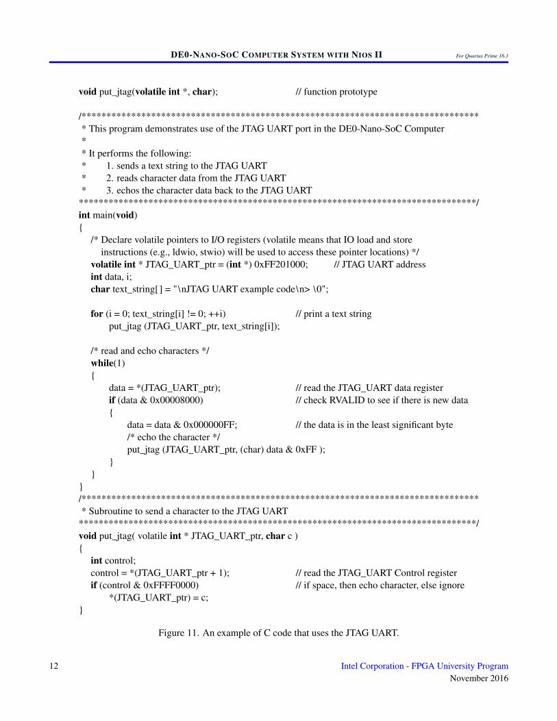
2.4.1 Using the JTAG UART with Assembly Language Code and C Code
Figures 10 and 11 give simple examples of assembly language and C code, respectively, that use the JTAG UART.Both versions of the code perform the same function, which is to first send an ASCII string to the JTAG UART, andthen enter an endless loop. In the loop, the code reads character data that has been received by the JTAG UART, andechoes this data back to the UART for transmission. If the program is executed by using the Intel FPGA MonitorProgram, then any keyboard character that is typed into the Terminal Window of the Monitor Program will be echoed
Intel Corporation - FPGA University ProgramNovember 2016
9
DE0-NANO-SOC COMPUTER SYSTEM WITH NIOS II For Quartus Prime 16.1
back, causing the character to appear in the Terminal Window.
The source code files shown in Figures 10 and 11 are made available as part of the Intel FPGA Monitor Program.The files can be found under the heading sample programs, and are identified by the name JTAG UART.
/********************************************************************************* This program demonstrates use of the JTAG UART port in the DE0-Nano-SoC Computer** It performs the following:* 1. sends a text string to the JTAG UART* 2. reads character data from the JTAG UART* 3. echos the character data back to the JTAG UART
********************************************************************************/.text /* executable code follows */.global _start
_start:/* set up stack pointer */movia sp, 0x00007FFC /* stack starts from highest address in onchip mem */
movia r6, 0xFF201000 /* JTAG UART base address */
/* print a text string */movia r8, TEXT_STRING
LOOP:ldb r5, 0(r8)beq r5, zero, GET_JTAG /* string is null-terminated */call PUT_JTAGaddi r8, r8, 1br LOOP
/* read and echo characters */GET_JTAG:
ldwio r4, 0(r6) /* read the JTAG UART data register */andi r8, r4, 0x8000 /* check if there is new data */beq r8, r0, GET_JTAG /* if no data, wait */andi r5, r4, 0x00ff /* the data is in the least significant byte */
call PUT_JTAG /* echo character */br GET_JTAG.end
Figure 10. An example of assembly language code that uses the JTAG UART (Part a).
10 Intel Corporation - FPGA University ProgramNovember 2016
DE0-NANO-SOC COMPUTER SYSTEM WITH NIOS II For Quartus Prime 16.1
/********************************************************************************* Subroutine to send a character to the JTAG UART* r5 = character to send* r6 = JTAG UART base address
********************************************************************************/.global PUT_JTAG
PUT_JTAG:/* save any modified registers */subi sp, sp, 4 /* reserve space on the stack */stw r4, 0(sp) /* save register */
ldwio r4, 4(r6) /* read the JTAG UART Control register */andhi r4, r4, 0xffff /* check for write space */beq r4, r0, END_PUT /* if no space, ignore the character */stwio r5, 0(r6) /* send the character */
END_PUT:/* restore registers */ldw r4, 0(sp)addi sp, sp, 4
ret
.data /* data follows */TEXT_STRING:
.asciz "\nJTAG UART example code\n> "
.end
Figure 10. An example of assembly language code that uses the JTAG UART (Part b).
Intel Corporation - FPGA University ProgramNovember 2016
11
DE0-NANO-SOC COMPUTER SYSTEM WITH NIOS II For Quartus Prime 16.1
void put_jtag(volatile int *, char); // function prototype
/********************************************************************************* This program demonstrates use of the JTAG UART port in the DE0-Nano-SoC Computer** It performs the following:* 1. sends a text string to the JTAG UART* 2. reads character data from the JTAG UART* 3. echos the character data back to the JTAG UART
********************************************************************************/int main(void){
/* Declare volatile pointers to I/O registers (volatile means that IO load and storeinstructions (e.g., ldwio, stwio) will be used to access these pointer locations) */
volatile int * JTAG_UART_ptr = (int *) 0xFF201000; // JTAG UART addressint data, i;char text_string[] = "\nJTAG UART example code\n> \0";
for (i = 0; text_string[i] != 0; ++i) // print a text stringput_jtag (JTAG_UART_ptr, text_string[i]);
/* read and echo characters */while(1){
data = *(JTAG_UART_ptr); // read the JTAG_UART data registerif (data & 0x00008000) // check RVALID to see if there is new data{
data = data & 0x000000FF; // the data is in the least significant byte/* echo the character */put_jtag (JTAG_UART_ptr, (char) data & 0xFF );
}}
}/********************************************************************************* Subroutine to send a character to the JTAG UART
********************************************************************************/void put_jtag( volatile int * JTAG_UART_ptr, char c ){
int control;control = *(JTAG_UART_ptr + 1); // read the JTAG_UART Control registerif (control & 0xFFFF0000) // if space, then echo character, else ignore
*(JTAG_UART_ptr) = c;}
Figure 11. An example of C code that uses the JTAG UART.
12 Intel Corporation - FPGA University ProgramNovember 2016
DE0-NANO-SOC COMPUTER SYSTEM WITH NIOS II For Quartus Prime 16.1
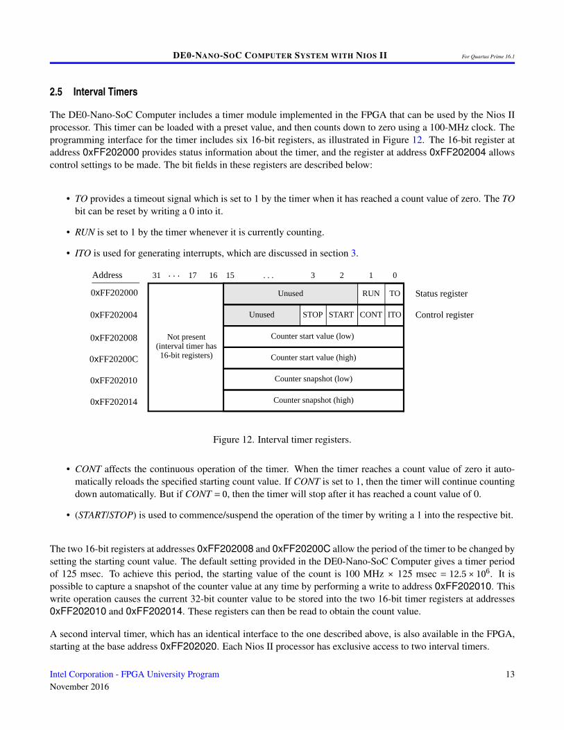
2.5 Interval Timers
The DE0-Nano-SoC Computer includes a timer module implemented in the FPGA that can be used by the Nios IIprocessor. This timer can be loaded with a preset value, and then counts down to zero using a 100-MHz clock. Theprogramming interface for the timer includes six 16-bit registers, as illustrated in Figure 12. The 16-bit register ataddress 0xFF202000 provides status information about the timer, and the register at address 0xFF202004 allowscontrol settings to be made. The bit fields in these registers are described below:
• TO provides a timeout signal which is set to 1 by the timer when it has reached a count value of zero. The TObit can be reset by writing a 0 into it.
• RUN is set to 1 by the timer whenever it is currently counting.
• ITO is used for generating interrupts, which are discussed in section 3.
Address 01531 . . .
0xFF202000
0xFF202004
. . .
Unused RUN TO
1
START CONT ITOSTOP
16 217
Unused
Counter start value (low) 0xFF202008
Counter start value (high)0xFF20200C
Counter snapshot (low)0xFF202010
Counter snapshot (high)0xFF202014
3
Not present(interval timer has16-bit registers)
Status register
Control register
Figure 12. Interval timer registers.
• CONT affects the continuous operation of the timer. When the timer reaches a count value of zero it auto-matically reloads the specified starting count value. If CONT is set to 1, then the timer will continue countingdown automatically. But if CONT = 0, then the timer will stop after it has reached a count value of 0.
• (START/STOP) is used to commence/suspend the operation of the timer by writing a 1 into the respective bit.
The two 16-bit registers at addresses 0xFF202008 and 0xFF20200C allow the period of the timer to be changed bysetting the starting count value. The default setting provided in the DE0-Nano-SoC Computer gives a timer periodof 125 msec. To achieve this period, the starting value of the count is 100 MHz × 125 msec = 12.5× 10⁶. It ispossible to capture a snapshot of the counter value at any time by performing a write to address 0xFF202010. Thiswrite operation causes the current 32-bit counter value to be stored into the two 16-bit timer registers at addresses0xFF202010 and 0xFF202014. These registers can then be read to obtain the count value.
A second interval timer, which has an identical interface to the one described above, is also available in the FPGA,starting at the base address 0xFF202020. Each Nios II processor has exclusive access to two interval timers.
Intel Corporation - FPGA University ProgramNovember 2016
13
DE0-NANO-SOC COMPUTER SYSTEM WITH NIOS II For Quartus Prime 16.1
3 Exceptions and Interrupts
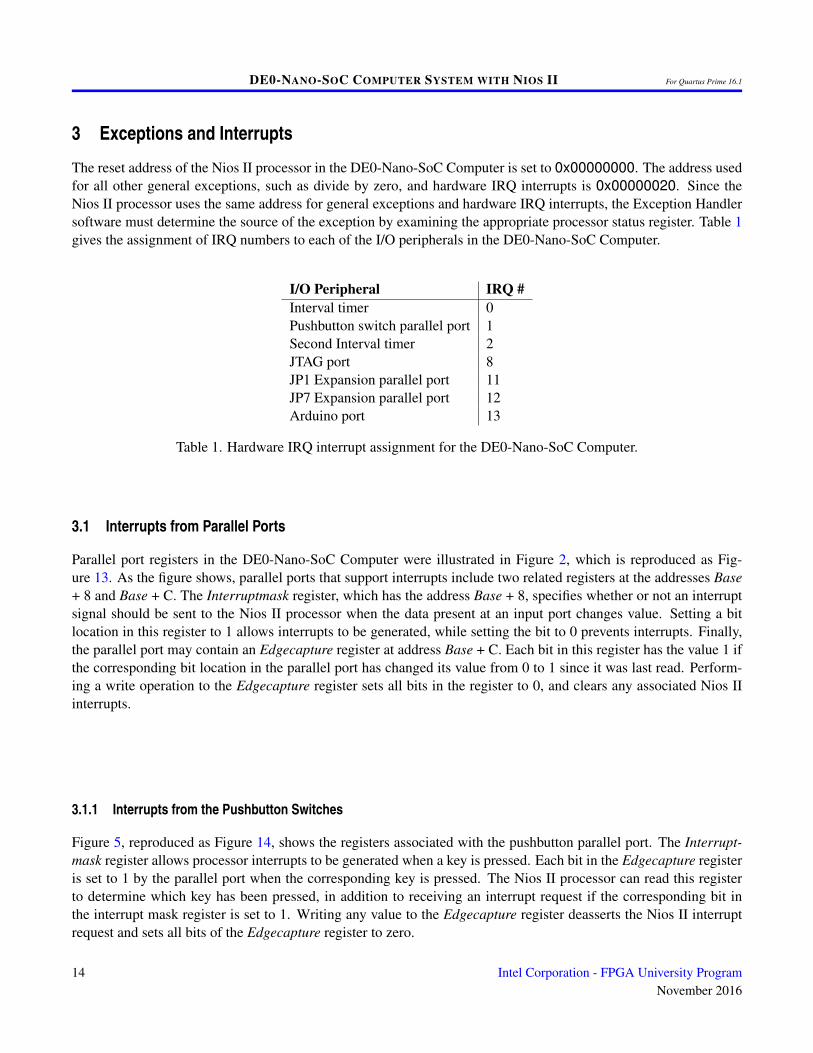
The reset address of the Nios II processor in the DE0-Nano-SoC Computer is set to 0x00000000. The address usedfor all other general exceptions, such as divide by zero, and hardware IRQ interrupts is 0x00000020. Since theNios II processor uses the same address for general exceptions and hardware IRQ interrupts, the Exception Handlersoftware must determine the source of the exception by examining the appropriate processor status register. Table 1gives the assignment of IRQ numbers to each of the I/O peripherals in the DE0-Nano-SoC Computer.
I/O Peripheral IRQ #Interval timer 0Pushbutton switch parallel port 1Second Interval timer 2JTAG port 8JP1 Expansion parallel port 11JP7 Expansion parallel port 12Arduino port 13
Table 1. Hardware IRQ interrupt assignment for the DE0-Nano-SoC Computer.
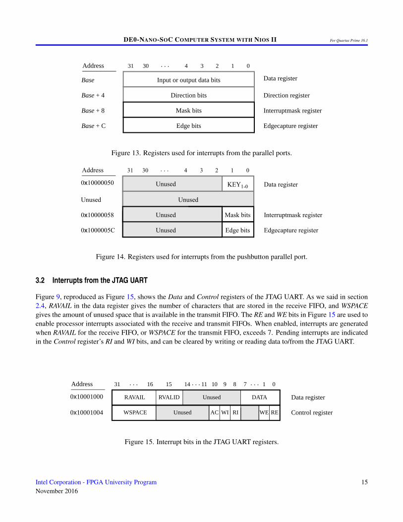
3.1 Interrupts from Parallel Ports
Parallel port registers in the DE0-Nano-SoC Computer were illustrated in Figure 2, which is reproduced as Fig-ure 13. As the figure shows, parallel ports that support interrupts include two related registers at the addresses Base+ 8 and Base + C. The Interruptmask register, which has the address Base + 8, specifies whether or not an interruptsignal should be sent to the Nios II processor when the data present at an input port changes value. Setting a bitlocation in this register to 1 allows interrupts to be generated, while setting the bit to 0 prevents interrupts. Finally,the parallel port may contain an Edgecapture register at address Base + C. Each bit in this register has the value 1 ifthe corresponding bit location in the parallel port has changed its value from 0 to 1 since it was last read. Perform-ing a write operation to the Edgecapture register sets all bits in the register to 0, and clears any associated Nios IIinterrupts.
3.1.1 Interrupts from the Pushbutton Switches
Figure 5, reproduced as Figure 14, shows the registers associated with the pushbutton parallel port. The Interrupt-mask register allows processor interrupts to be generated when a key is pressed. Each bit in the Edgecapture registeris set to 1 by the parallel port when the corresponding key is pressed. The Nios II processor can read this registerto determine which key has been pressed, in addition to receiving an interrupt request if the corresponding bit inthe interrupt mask register is set to 1. Writing any value to the Edgecapture register deasserts the Nios II interruptrequest and sets all bits of the Edgecapture register to zero.
14 Intel Corporation - FPGA University ProgramNovember 2016
DE0-NANO-SOC COMPUTER SYSTEM WITH NIOS II For Quartus Prime 16.1
Address 02 14 331 30 . . .
Base
Base + 8
Base + C
Base + 4
Input or output data bits
Direction bits
Data register
Direction register
Interruptmask register
Edgecapture register Edge bits
Mask bits
Direction bits
Figure 13. Registers used for interrupts from the parallel ports.
Address 02 14 331 30 . . .
0x10000050
0x10000058
0x1000005C
Unused
KEY1-0Unused Data register
Interruptmask register
Edgecapture register
Unused
Edge bits
Mask bitsUnused
Unused
Figure 14. Registers used for interrupts from the pushbutton parallel port.
3.2 Interrupts from the JTAG UART
Figure 9, reproduced as Figure 15, shows the Data and Control registers of the JTAG UART. As we said in section2.4, RAVAIL in the data register gives the number of characters that are stored in the receive FIFO, and WSPACEgives the amount of unused space that is available in the transmit FIFO. The RE and WE bits in Figure 15 are used toenable processor interrupts associated with the receive and transmit FIFOs. When enabled, interrupts are generatedwhen RAVAIL for the receive FIFO, or WSPACE for the transmit FIFO, exceeds 7. Pending interrupts are indicatedin the Control register’s RI and WI bits, and can be cleared by writing or reading data to/from the JTAG UART.
Address 0731 16. . .
0x10001000
0x10001004
DATARAVAIL
14 8. . . . . .
WSPACE Unused WI RI WE RE
1
RVALID
AC
10 911
Unused
15
Data register
Control register
Figure 15. Interrupt bits in the JTAG UART registers.
Intel Corporation - FPGA University ProgramNovember 2016
15
DE0-NANO-SOC COMPUTER SYSTEM WITH NIOS II For Quartus Prime 16.1
3.3 Interrupts from the Interval Timer
Figure 12, in section 2.5, shows six registers that are associated with the interval timer. As we said in section 2.5,the bit b0 (TO) is set to 1 when the timer reaches a count value of 0. It is possible to generate an interrupt when thisoccurs, by using the bit b16 (ITO). Setting the bit ITO to 1 allows an interrupt request to be generated whenever TObecomes 1. After an interrupt occurs, it can be cleared by writing any value to the register that contains the bit TO.
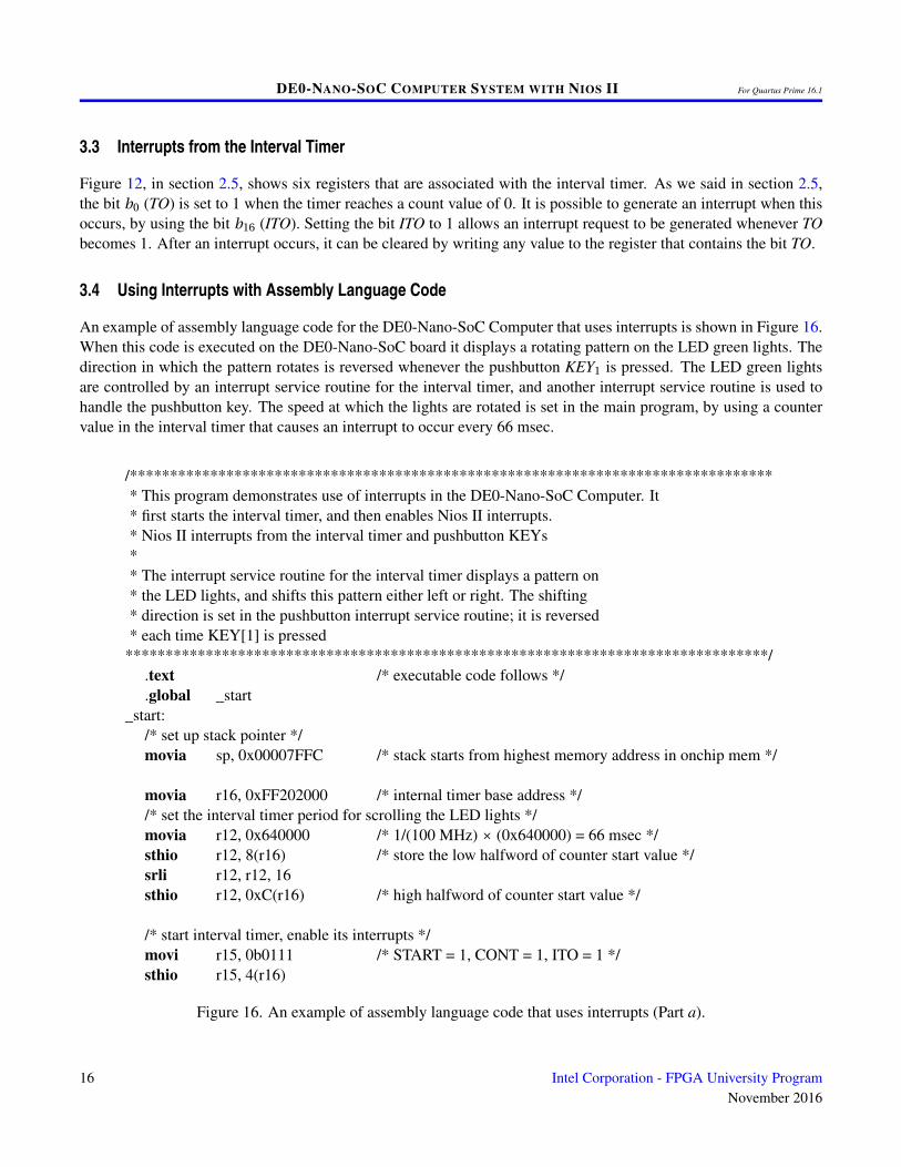
3.4 Using Interrupts with Assembly Language Code
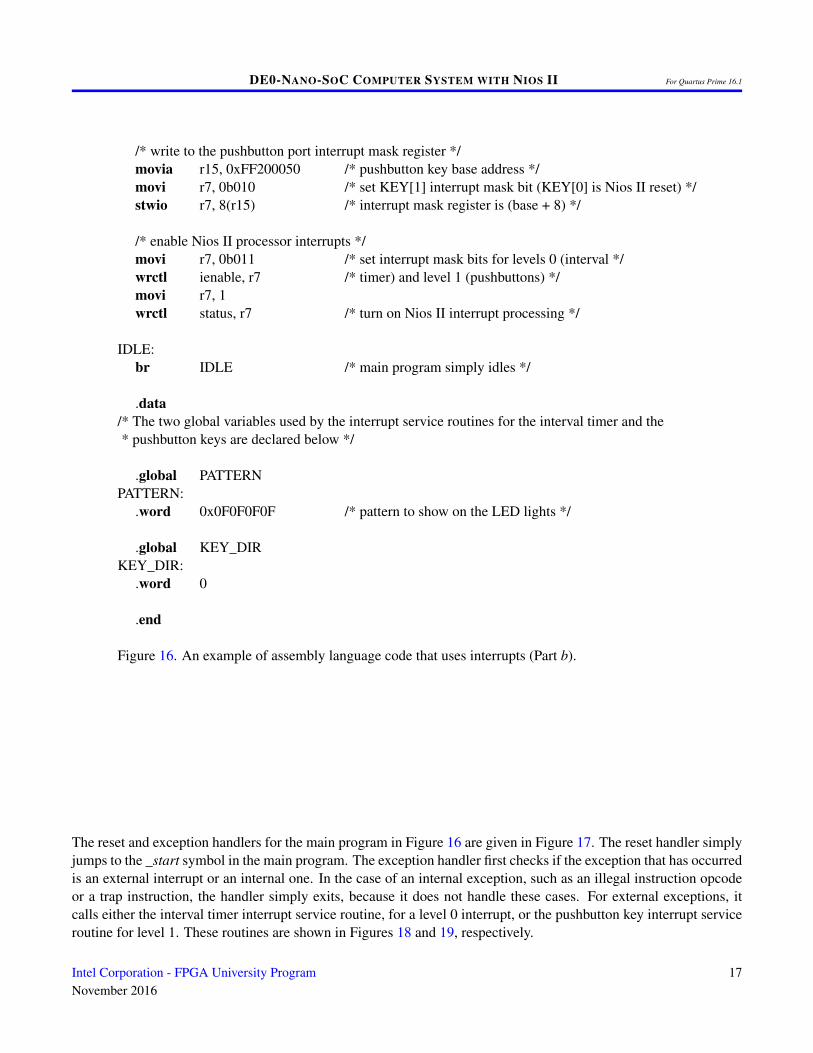
An example of assembly language code for the DE0-Nano-SoC Computer that uses interrupts is shown in Figure 16.When this code is executed on the DE0-Nano-SoC board it displays a rotating pattern on the LED green lights. Thedirection in which the pattern rotates is reversed whenever the pushbutton KEY1 is pressed. The LED green lightsare controlled by an interrupt service routine for the interval timer, and another interrupt service routine is used tohandle the pushbutton key. The speed at which the lights are rotated is set in the main program, by using a countervalue in the interval timer that causes an interrupt to occur every 66 msec.
/********************************************************************************* This program demonstrates use of interrupts in the DE0-Nano-SoC Computer. It* first starts the interval timer, and then enables Nios II interrupts.* Nios II interrupts from the interval timer and pushbutton KEYs** The interrupt service routine for the interval timer displays a pattern on* the LED lights, and shifts this pattern either left or right. The shifting* direction is set in the pushbutton interrupt service routine; it is reversed* each time KEY[1] is pressed
********************************************************************************/.text /* executable code follows */.global _start
_start:/* set up stack pointer */movia sp, 0x00007FFC /* stack starts from highest memory address in onchip mem */
movia r16, 0xFF202000 /* internal timer base address *//* set the interval timer period for scrolling the LED lights */movia r12, 0x640000 /* 1/(100 MHz) × (0x640000) = 66 msec */sthio r12, 8(r16) /* store the low halfword of counter start value */srli r12, r12, 16sthio r12, 0xC(r16) /* high halfword of counter start value */
/* start interval timer, enable its interrupts */movi r15, 0b0111 /* START = 1, CONT = 1, ITO = 1 */sthio r15, 4(r16)
Figure 16. An example of assembly language code that uses interrupts (Part a).
16 Intel Corporation - FPGA University ProgramNovember 2016
DE0-NANO-SOC COMPUTER SYSTEM WITH NIOS II For Quartus Prime 16.1
/* write to the pushbutton port interrupt mask register */movia r15, 0xFF200050 /* pushbutton key base address */movi r7, 0b010 /* set KEY[1] interrupt mask bit (KEY[0] is Nios II reset) */stwio r7, 8(r15) /* interrupt mask register is (base + 8) */
/* enable Nios II processor interrupts */movi r7, 0b011 /* set interrupt mask bits for levels 0 (interval */wrctl ienable, r7 /* timer) and level 1 (pushbuttons) */movi r7, 1wrctl status, r7 /* turn on Nios II interrupt processing */
IDLE:br IDLE /* main program simply idles */
.data/* The two global variables used by the interrupt service routines for the interval timer and the* pushbutton keys are declared below */
.global PATTERNPATTERN:
.word 0x0F0F0F0F /* pattern to show on the LED lights */
.global KEY_DIRKEY_DIR:
.word 0
.end
Figure 16. An example of assembly language code that uses interrupts (Part b).
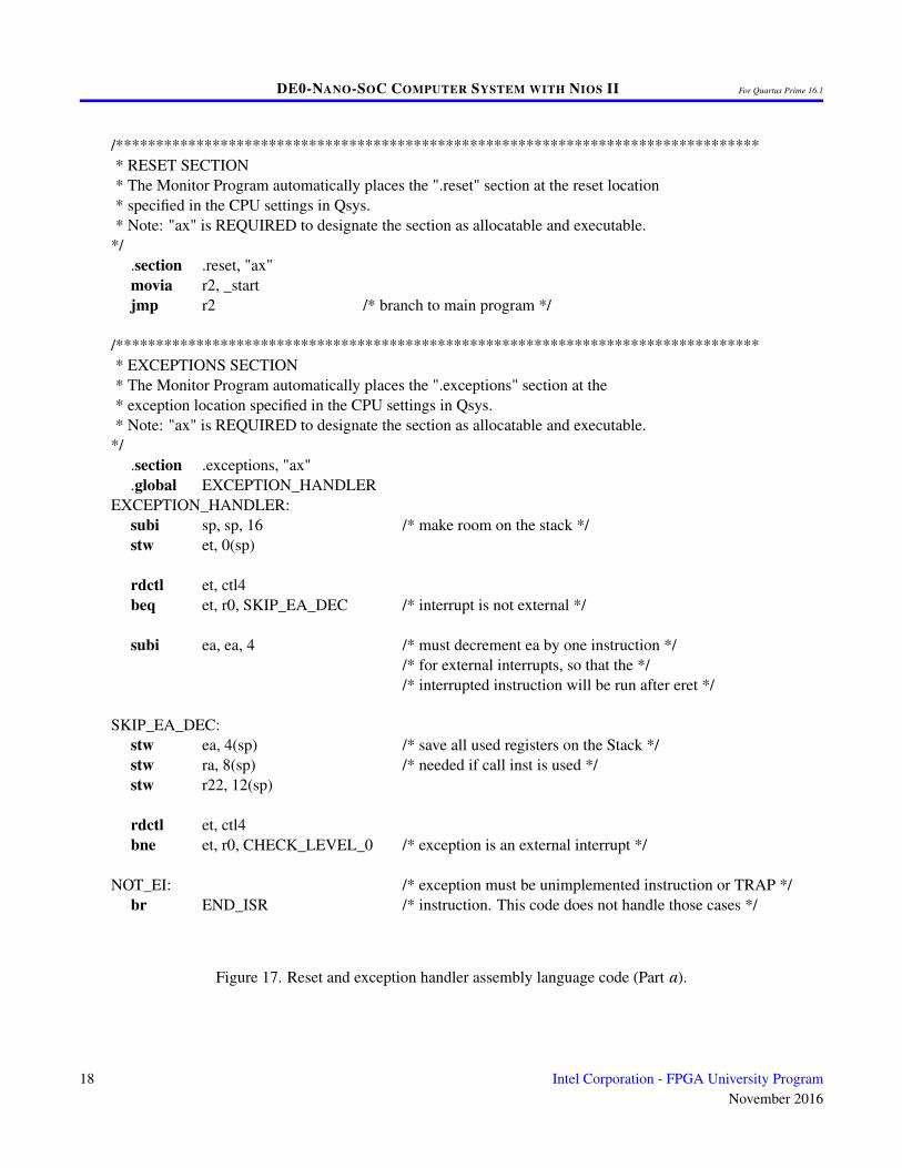
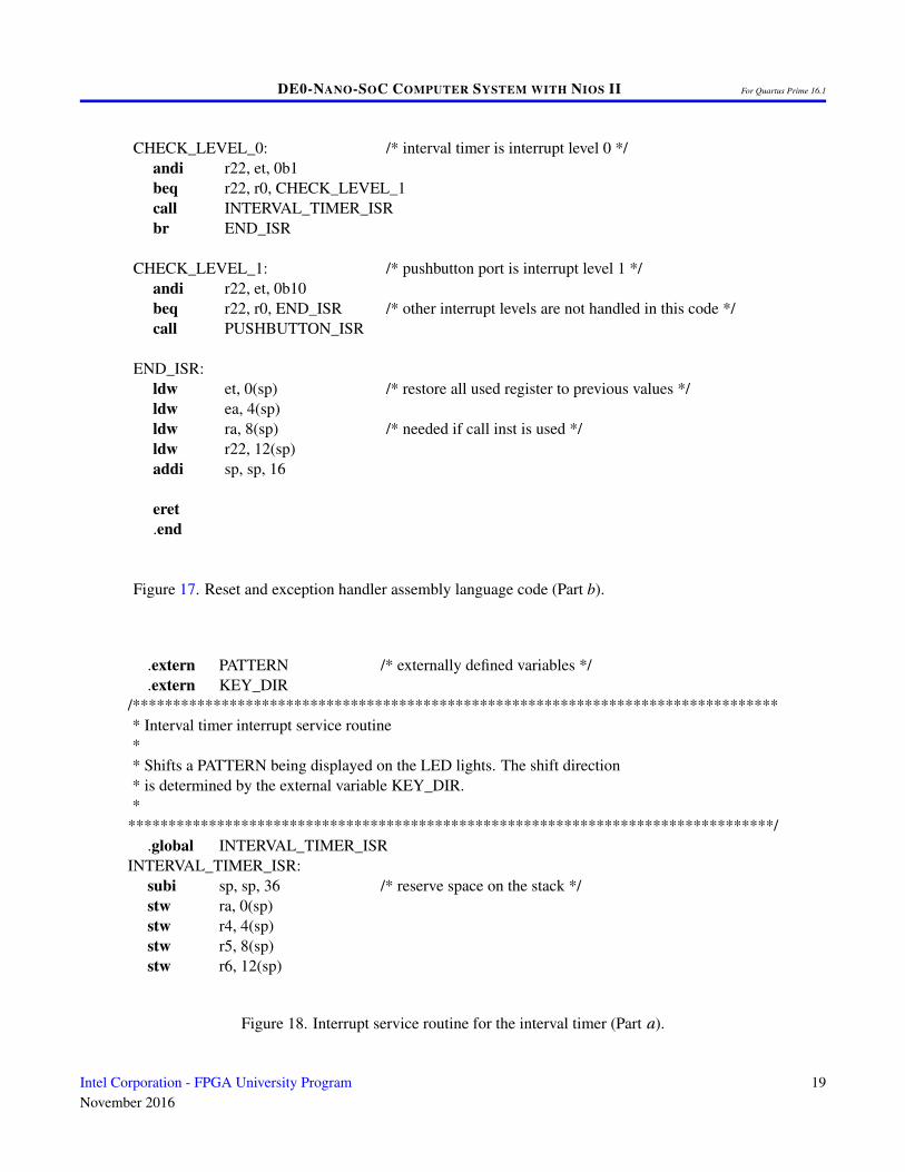
The reset and exception handlers for the main program in Figure 16 are given in Figure 17. The reset handler simplyjumps to the _start symbol in the main program. The exception handler first checks if the exception that has occurredis an external interrupt or an internal one. In the case of an internal exception, such as an illegal instruction opcodeor a trap instruction, the handler simply exits, because it does not handle these cases. For external exceptions, itcalls either the interval timer interrupt service routine, for a level 0 interrupt, or the pushbutton key interrupt serviceroutine for level 1. These routines are shown in Figures 18 and 19, respectively.
Intel Corporation - FPGA University ProgramNovember 2016
17
DE0-NANO-SOC COMPUTER SYSTEM WITH NIOS II For Quartus Prime 16.1
/********************************************************************************* RESET SECTION* The Monitor Program automatically places the ".reset" section at the reset location* specified in the CPU settings in Qsys.* Note: "ax" is REQUIRED to designate the section as allocatable and executable.
*/.section .reset, "ax"movia r2, _startjmp r2 /* branch to main program */
/********************************************************************************* EXCEPTIONS SECTION* The Monitor Program automatically places the ".exceptions" section at the* exception location specified in the CPU settings in Qsys.* Note: "ax" is REQUIRED to designate the section as allocatable and executable.
*/.section .exceptions, "ax".global EXCEPTION_HANDLER
EXCEPTION_HANDLER:subi sp, sp, 16 /* make room on the stack */stw et, 0(sp)
rdctl et, ctl4beq et, r0, SKIP_EA_DEC /* interrupt is not external */
subi ea, ea, 4 /* must decrement ea by one instruction *//* for external interrupts, so that the *//* interrupted instruction will be run after eret */
SKIP_EA_DEC:stw ea, 4(sp) /* save all used registers on the Stack */stw ra, 8(sp) /* needed if call inst is used */stw r22, 12(sp)
rdctl et, ctl4bne et, r0, CHECK_LEVEL_0 /* exception is an external interrupt */
NOT_EI: /* exception must be unimplemented instruction or TRAP */br END_ISR /* instruction. This code does not handle those cases */
Figure 17. Reset and exception handler assembly language code (Part a).
18 Intel Corporation - FPGA University ProgramNovember 2016
DE0-NANO-SOC COMPUTER SYSTEM WITH NIOS II For Quartus Prime 16.1
CHECK_LEVEL_0: /* interval timer is interrupt level 0 */andi r22, et, 0b1beq r22, r0, CHECK_LEVEL_1call INTERVAL_TIMER_ISRbr END_ISR
CHECK_LEVEL_1: /* pushbutton port is interrupt level 1 */andi r22, et, 0b10beq r22, r0, END_ISR /* other interrupt levels are not handled in this code */call PUSHBUTTON_ISR
END_ISR:ldw et, 0(sp) /* restore all used register to previous values */ldw ea, 4(sp)ldw ra, 8(sp) /* needed if call inst is used */ldw r22, 12(sp)addi sp, sp, 16
eret.end
Figure 17. Reset and exception handler assembly language code (Part b).
.extern PATTERN /* externally defined variables */
.extern KEY_DIR/********************************************************************************* Interval timer interrupt service routine** Shifts a PATTERN being displayed on the LED lights. The shift direction* is determined by the external variable KEY_DIR.*
********************************************************************************/.global INTERVAL_TIMER_ISR
INTERVAL_TIMER_ISR:subi sp, sp, 36 /* reserve space on the stack */stw ra, 0(sp)stw r4, 4(sp)stw r5, 8(sp)stw r6, 12(sp)
Figure 18. Interrupt service routine for the interval timer (Part a).
Intel Corporation - FPGA University ProgramNovember 2016
19
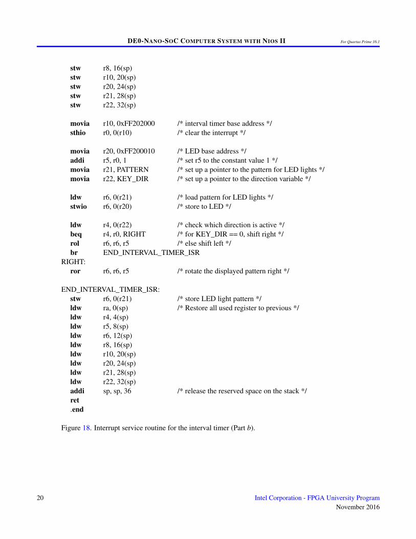
DE0-NANO-SOC COMPUTER SYSTEM WITH NIOS II For Quartus Prime 16.1
stw r8, 16(sp)stw r10, 20(sp)stw r20, 24(sp)stw r21, 28(sp)stw r22, 32(sp)
movia r10, 0xFF202000 /* interval timer base address */sthio r0, 0(r10) /* clear the interrupt */
movia r20, 0xFF200010 /* LED base address */addi r5, r0, 1 /* set r5 to the constant value 1 */movia r21, PATTERN /* set up a pointer to the pattern for LED lights */movia r22, KEY_DIR /* set up a pointer to the direction variable */
ldw r6, 0(r21) /* load pattern for LED lights */stwio r6, 0(r20) /* store to LED */
ldw r4, 0(r22) /* check which direction is active */beq r4, r0, RIGHT /* for KEY_DIR == 0, shift right */rol r6, r6, r5 /* else shift left */br END_INTERVAL_TIMER_ISR
RIGHT:ror r6, r6, r5 /* rotate the displayed pattern right */
END_INTERVAL_TIMER_ISR:stw r6, 0(r21) /* store LED light pattern */ldw ra, 0(sp) /* Restore all used register to previous */ldw r4, 4(sp)ldw r5, 8(sp)ldw r6, 12(sp)ldw r8, 16(sp)ldw r10, 20(sp)ldw r20, 24(sp)ldw r21, 28(sp)ldw r22, 32(sp)addi sp, sp, 36 /* release the reserved space on the stack */ret.end
Figure 18. Interrupt service routine for the interval timer (Part b).
20 Intel Corporation - FPGA University ProgramNovember 2016
DE0-NANO-SOC COMPUTER SYSTEM WITH NIOS II For Quartus Prime 16.1
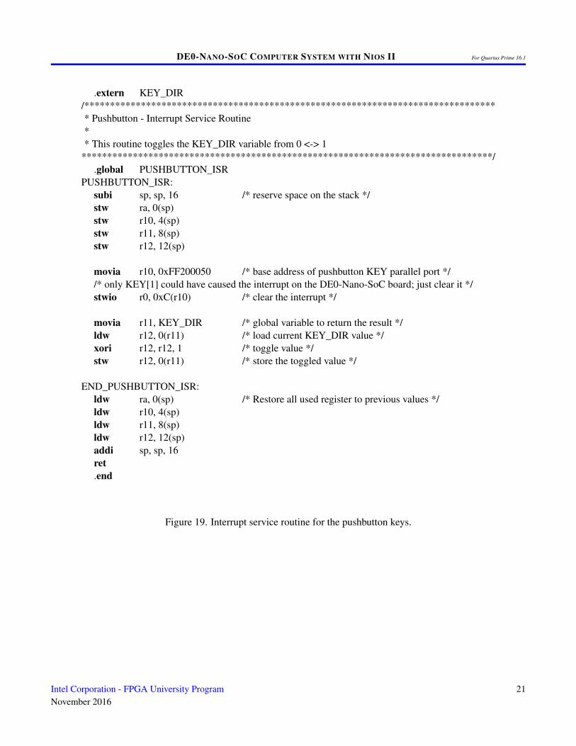
.extern KEY_DIR/********************************************************************************* Pushbutton - Interrupt Service Routine** This routine toggles the KEY_DIR variable from 0 <-> 1
********************************************************************************/.global PUSHBUTTON_ISR
PUSHBUTTON_ISR:subi sp, sp, 16 /* reserve space on the stack */stw ra, 0(sp)stw r10, 4(sp)stw r11, 8(sp)stw r12, 12(sp)
movia r10, 0xFF200050 /* base address of pushbutton KEY parallel port *//* only KEY[1] could have caused the interrupt on the DE0-Nano-SoC board; just clear it */stwio r0, 0xC(r10) /* clear the interrupt */
movia r11, KEY_DIR /* global variable to return the result */ldw r12, 0(r11) /* load current KEY_DIR value */xori r12, r12, 1 /* toggle value */stw r12, 0(r11) /* store the toggled value */
END_PUSHBUTTON_ISR:ldw ra, 0(sp) /* Restore all used register to previous values */ldw r10, 4(sp)ldw r11, 8(sp)ldw r12, 12(sp)addi sp, sp, 16ret.end
Figure 19. Interrupt service routine for the pushbutton keys.
Intel Corporation - FPGA University ProgramNovember 2016
21
DE0-NANO-SOC COMPUTER SYSTEM WITH NIOS II For Quartus Prime 16.1
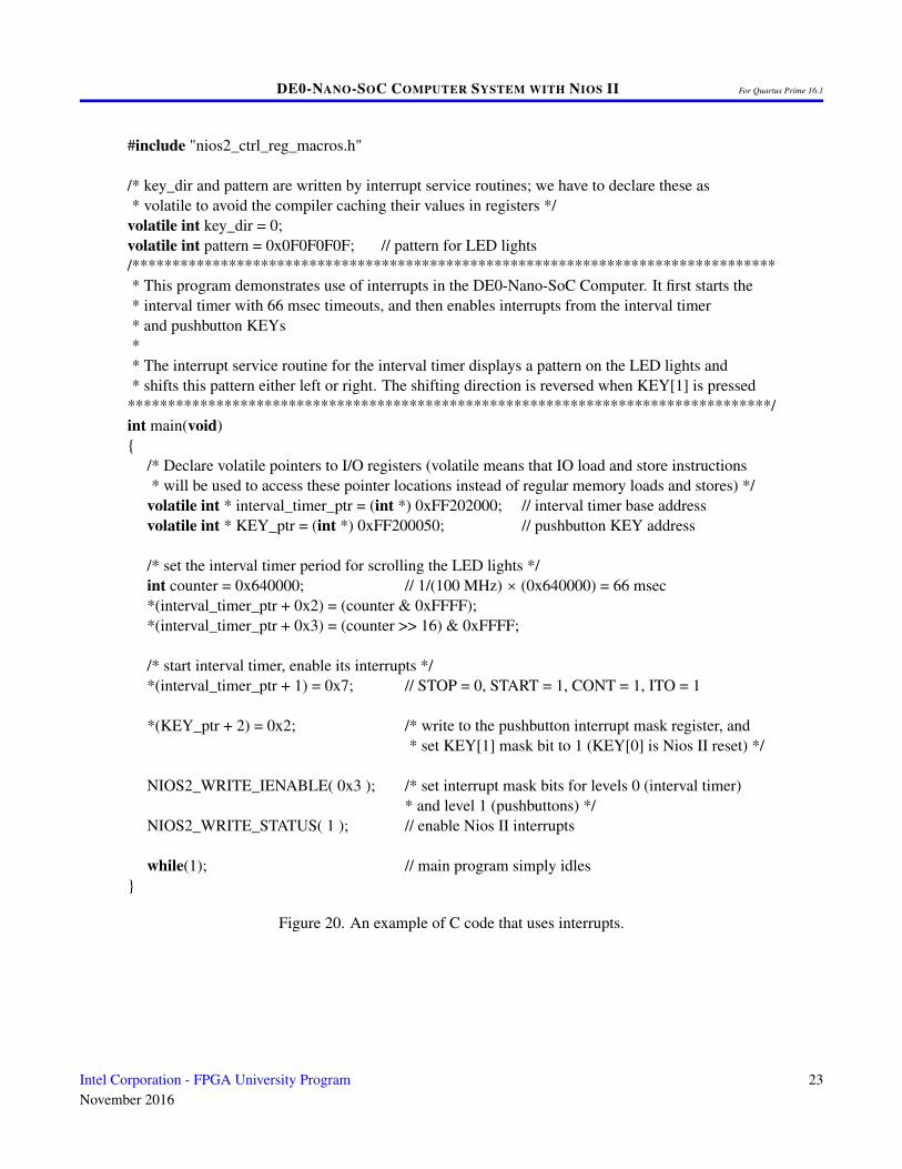
3.5 Using Interrupts with C Language Code
An example of C language code for the DE0-Nano-SoC Computer that uses interrupts is shown in Figure 20. Thiscode performs exactly the same operations as the code described in Figure 16.
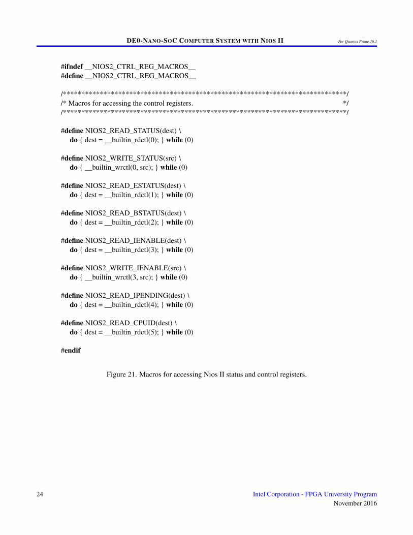
To enable interrupts the code in Figure 20 uses macros that provide access to the Nios II status and control registers.A collection of such macros, which can be used in any C program, are provided in Figure 21.
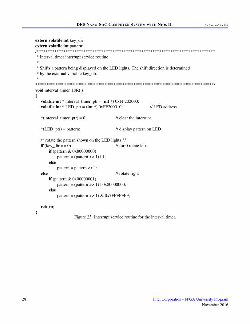
The reset and exception handlers for the main program in Figure 20 are given in Figure 22. The function calledthe_reset provides a simple reset mechanism by performing a branch to the main program. The function namedthe_exception represents a general exception handler that can be used with any C program. It includes assemblylanguage code to check if the exception is caused by an external interrupt, and, if so, calls a C language routinenamed interrupt_handler. This routine can then perform whatever action is needed for the specific application.In Figure 22, the interrupt_handler code first determines which exception has occurred, by using a macro fromFigure 21 that reads the content of the Nios II interrupt pending register. The interrupt service routine that isinvoked for the interval timer is shown in 23, and the interrupt service routine for the pushbutton switches appearsin Figure 24.
The source code files shown in Figure 16 to Figure 24 are distributed as part of the Intel FPGA Monitor Program.The files can be found under the heading sample programs, and are identified by the name Interrupt Example.
22 Intel Corporation - FPGA University ProgramNovember 2016
DE0-NANO-SOC COMPUTER SYSTEM WITH NIOS II For Quartus Prime 16.1
#include "nios2_ctrl_reg_macros.h"
/* key_dir and pattern are written by interrupt service routines; we have to declare these as* volatile to avoid the compiler caching their values in registers */
volatile int key_dir = 0;volatile int pattern = 0x0F0F0F0F; // pattern for LED lights/********************************************************************************* This program demonstrates use of interrupts in the DE0-Nano-SoC Computer. It first starts the* interval timer with 66 msec timeouts, and then enables interrupts from the interval timer* and pushbutton KEYs** The interrupt service routine for the interval timer displays a pattern on the LED lights and* shifts this pattern either left or right. The shifting direction is reversed when KEY[1] is pressed
********************************************************************************/int main(void){
/* Declare volatile pointers to I/O registers (volatile means that IO load and store instructions* will be used to access these pointer locations instead of regular memory loads and stores) */
volatile int * interval_timer_ptr = (int *) 0xFF202000; // interval timer base addressvolatile int * KEY_ptr = (int *) 0xFF200050; // pushbutton KEY address
/* set the interval timer period for scrolling the LED lights */int counter = 0x640000; // 1/(100 MHz) × (0x640000) = 66 msec*(interval_timer_ptr + 0x2) = (counter & 0xFFFF);*(interval_timer_ptr + 0x3) = (counter >> 16) & 0xFFFF;
/* start interval timer, enable its interrupts */*(interval_timer_ptr + 1) = 0x7; // STOP = 0, START = 1, CONT = 1, ITO = 1
*(KEY_ptr + 2) = 0x2; /* write to the pushbutton interrupt mask register, and* set KEY[1] mask bit to 1 (KEY[0] is Nios II reset) */
NIOS2_WRITE_IENABLE( 0x3 ); /* set interrupt mask bits for levels 0 (interval timer)* and level 1 (pushbuttons) */
NIOS2_WRITE_STATUS( 1 ); // enable Nios II interrupts
while(1); // main program simply idles}
Figure 20. An example of C code that uses interrupts.
Intel Corporation - FPGA University ProgramNovember 2016
23
DE0-NANO-SOC COMPUTER SYSTEM WITH NIOS II For Quartus Prime 16.1
#ifndef __NIOS2_CTRL_REG_MACROS__#define __NIOS2_CTRL_REG_MACROS__
/*****************************************************************************//* Macros for accessing the control registers. *//*****************************************************************************/
#define NIOS2_READ_STATUS(dest) \do { dest = __builtin_rdctl(0); } while (0)
#define NIOS2_WRITE_STATUS(src) \do { __builtin_wrctl(0, src); } while (0)
#define NIOS2_READ_ESTATUS(dest) \do { dest = __builtin_rdctl(1); } while (0)
#define NIOS2_READ_BSTATUS(dest) \do { dest = __builtin_rdctl(2); } while (0)
#define NIOS2_READ_IENABLE(dest) \do { dest = __builtin_rdctl(3); } while (0)
#define NIOS2_WRITE_IENABLE(src) \do { __builtin_wrctl(3, src); } while (0)
#define NIOS2_READ_IPENDING(dest) \do { dest = __builtin_rdctl(4); } while (0)
#define NIOS2_READ_CPUID(dest) \do { dest = __builtin_rdctl(5); } while (0)
#endif
Figure 21. Macros for accessing Nios II status and control registers.
24 Intel Corporation - FPGA University ProgramNovember 2016
DE0-NANO-SOC COMPUTER SYSTEM WITH NIOS II For Quartus Prime 16.1
#include "nios2_ctrl_reg_macros.h"
/* function prototypes */void main(void);void interrupt_handler(void);void interval_timer_ISR(void);void pushbutton_ISR(void);
/* The assembly language code below handles Nios II reset processing */void the_reset (void) __attribute__ ((section (".reset")));void the_reset (void)/******************************************************************************** Reset code; by using the section attribute with the name ".reset" we allow the linker program* to locate this code at the proper reset vector address. This code just calls the main program******************************************************************************/
{asm (".set noat"); /* Instruct the assembler NOT to use reg at (r1) as
* a temp register for performing optimizations */asm (".set nobreak"); /* Suppresses a warning message that says that some
* debuggers corrupt regs bt (r25) and ba (r30) */asm ("movia r2, _start"); // call the C language main programasm ("jmp r2");
}/* The assembly language code below handles Nios II exception processing. This code should not be* modified; instead, the C language code in the function interrupt_handler() can be modified as* needed for a given application. */
void the_exception (void) __attribute__ ((section (".exceptions")));void the_exception (void)/******************************************************************************** Exceptions code; by giving the code a section attribute with the name ".exceptions" we allow* the linker to locate this code at the proper exceptions vector address. This code calls the* interrupt handler and later returns from the exception.******************************************************************************/
{asm (".set noat"); // magic, for the C compilerasm (".set nobreak"); // magic, for the C compilerasm ( "subi sp, sp, 128");asm ( "stw et, 96(sp)");asm ( "rdctl et, ctl4");asm ( "beq et, r0, SKIP_EA_DEC"); // interrupt is not externalasm ( "subi ea, ea, 4"); /* must decrement ea by one instruction for external
* interrupts, so that the instruction will be run */
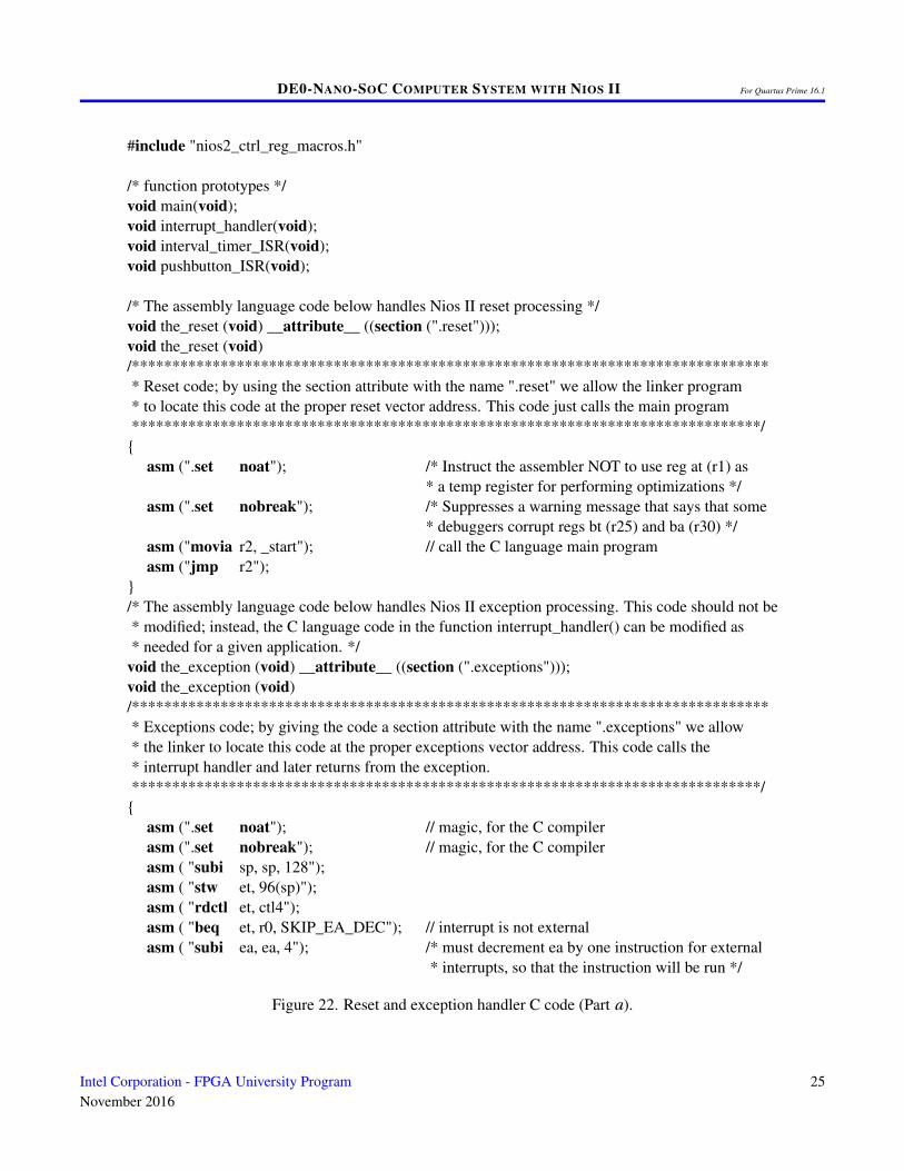
Figure 22. Reset and exception handler C code (Part a).
Intel Corporation - FPGA University ProgramNovember 2016
25
DE0-NANO-SOC COMPUTER SYSTEM WITH NIOS II For Quartus Prime 16.1
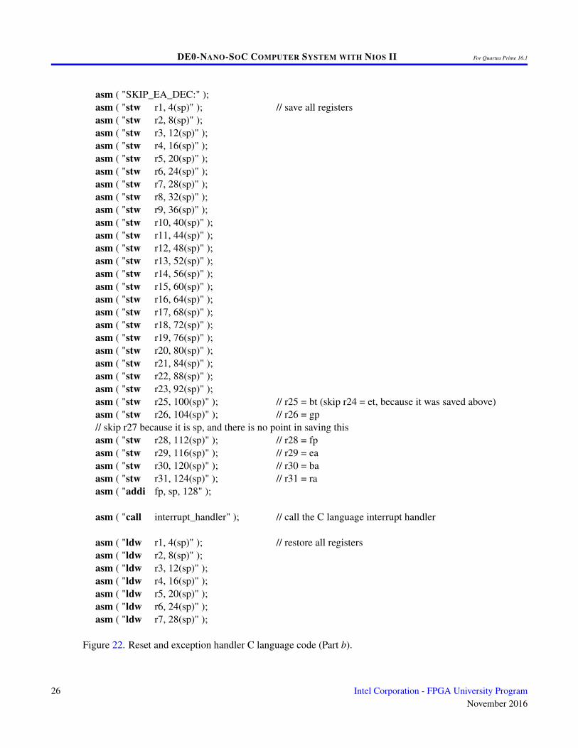
asm ( "SKIP_EA_DEC:" );asm ( "stw r1, 4(sp)" ); // save all registersasm ( "stw r2, 8(sp)" );asm ( "stw r3, 12(sp)" );asm ( "stw r4, 16(sp)" );asm ( "stw r5, 20(sp)" );asm ( "stw r6, 24(sp)" );asm ( "stw r7, 28(sp)" );asm ( "stw r8, 32(sp)" );asm ( "stw r9, 36(sp)" );asm ( "stw r10, 40(sp)" );asm ( "stw r11, 44(sp)" );asm ( "stw r12, 48(sp)" );asm ( "stw r13, 52(sp)" );asm ( "stw r14, 56(sp)" );asm ( "stw r15, 60(sp)" );asm ( "stw r16, 64(sp)" );asm ( "stw r17, 68(sp)" );asm ( "stw r18, 72(sp)" );asm ( "stw r19, 76(sp)" );asm ( "stw r20, 80(sp)" );asm ( "stw r21, 84(sp)" );asm ( "stw r22, 88(sp)" );asm ( "stw r23, 92(sp)" );asm ( "stw r25, 100(sp)" ); // r25 = bt (skip r24 = et, because it was saved above)asm ( "stw r26, 104(sp)" ); // r26 = gp// skip r27 because it is sp, and there is no point in saving thisasm ( "stw r28, 112(sp)" ); // r28 = fpasm ( "stw r29, 116(sp)" ); // r29 = eaasm ( "stw r30, 120(sp)" ); // r30 = baasm ( "stw r31, 124(sp)" ); // r31 = raasm ( "addi fp, sp, 128" );
asm ( "call interrupt_handler" ); // call the C language interrupt handler
asm ( "ldw r1, 4(sp)" ); // restore all registersasm ( "ldw r2, 8(sp)" );asm ( "ldw r3, 12(sp)" );asm ( "ldw r4, 16(sp)" );asm ( "ldw r5, 20(sp)" );asm ( "ldw r6, 24(sp)" );asm ( "ldw r7, 28(sp)" );
Figure 22. Reset and exception handler C language code (Part b).
26 Intel Corporation - FPGA University ProgramNovember 2016
DE0-NANO-SOC COMPUTER SYSTEM WITH NIOS II For Quartus Prime 16.1
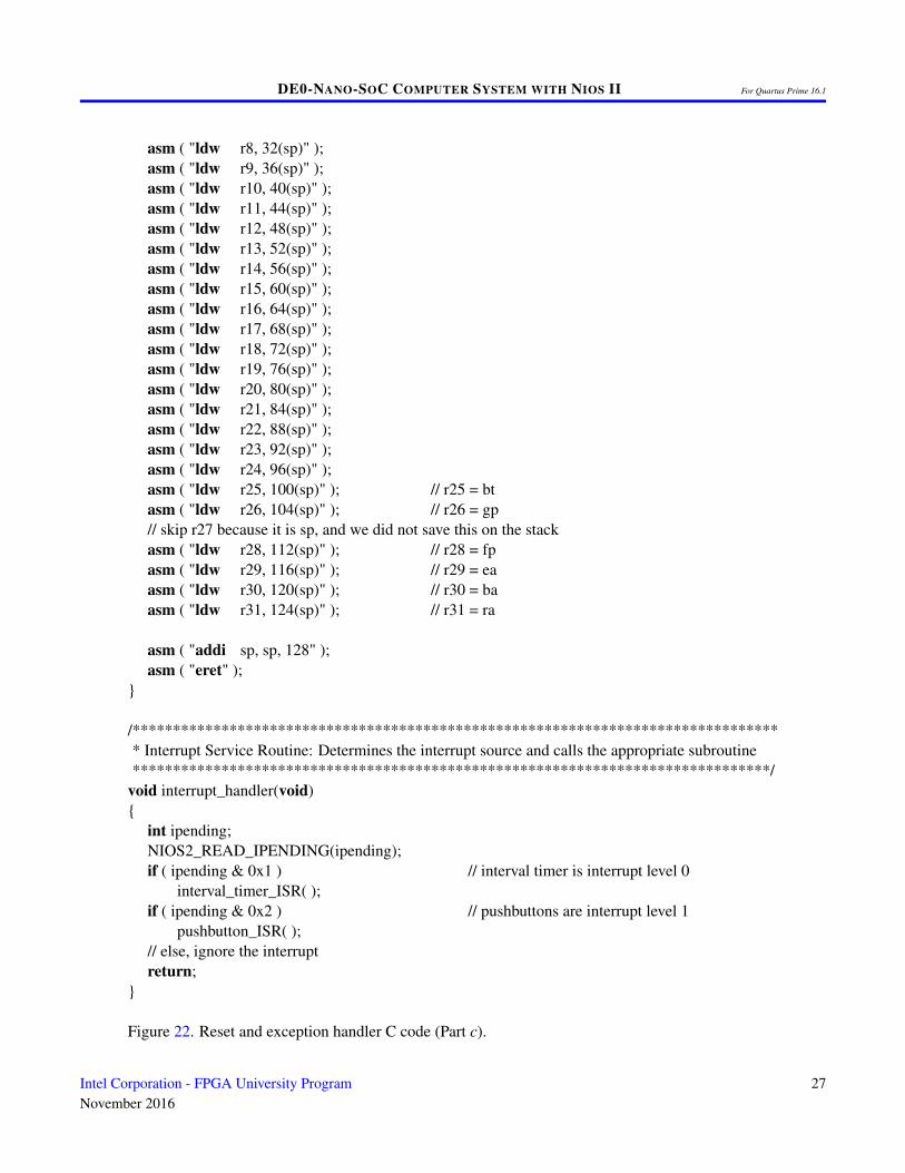
asm ( "ldw r8, 32(sp)" );asm ( "ldw r9, 36(sp)" );asm ( "ldw r10, 40(sp)" );asm ( "ldw r11, 44(sp)" );asm ( "ldw r12, 48(sp)" );asm ( "ldw r13, 52(sp)" );asm ( "ldw r14, 56(sp)" );asm ( "ldw r15, 60(sp)" );asm ( "ldw r16, 64(sp)" );asm ( "ldw r17, 68(sp)" );asm ( "ldw r18, 72(sp)" );asm ( "ldw r19, 76(sp)" );asm ( "ldw r20, 80(sp)" );asm ( "ldw r21, 84(sp)" );asm ( "ldw r22, 88(sp)" );asm ( "ldw r23, 92(sp)" );asm ( "ldw r24, 96(sp)" );asm ( "ldw r25, 100(sp)" ); // r25 = btasm ( "ldw r26, 104(sp)" ); // r26 = gp// skip r27 because it is sp, and we did not save this on the stackasm ( "ldw r28, 112(sp)" ); // r28 = fpasm ( "ldw r29, 116(sp)" ); // r29 = eaasm ( "ldw r30, 120(sp)" ); // r30 = baasm ( "ldw r31, 124(sp)" ); // r31 = ra
asm ( "addi sp, sp, 128" );asm ( "eret" );
}
/********************************************************************************* Interrupt Service Routine: Determines the interrupt source and calls the appropriate subroutine*******************************************************************************/
void interrupt_handler(void){
int ipending;NIOS2_READ_IPENDING(ipending);if ( ipending & 0x1 ) // interval timer is interrupt level 0
interval_timer_ISR( );if ( ipending & 0x2 ) // pushbuttons are interrupt level 1
pushbutton_ISR( );// else, ignore the interruptreturn;
}
Figure 22. Reset and exception handler C code (Part c).
Intel Corporation - FPGA University ProgramNovember 2016
27
DE0-NANO-SOC COMPUTER SYSTEM WITH NIOS II For Quartus Prime 16.1
extern volatile int key_dir;extern volatile int pattern;/********************************************************************************* Interval timer interrupt service routine** Shifts a pattern being displayed on the LED lights. The shift direction is determined* by the external variable key_dir.*
********************************************************************************/void interval_timer_ISR( ){
volatile int * interval_timer_ptr = (int *) 0xFF202000;volatile int * LED_ptr = (int *) 0xFF200010; // LED address
*(interval_timer_ptr) = 0; // clear the interrupt
*(LED_ptr) = pattern; // display pattern on LED
/* rotate the pattern shown on the LED lights */if (key_dir == 0) // for 0 rotate left
if (pattern & 0x80000000)pattern = (pattern << 1) | 1;
elsepattern = pattern << 1;
else // rotate rightif (pattern & 0x00000001)
pattern = (pattern >> 1) | 0x80000000;else
pattern = (pattern >> 1) & 0x7FFFFFFF;
return;}
Figure 23. Interrupt service routine for the interval timer.
28 Intel Corporation - FPGA University ProgramNovember 2016
DE0-NANO-SOC COMPUTER SYSTEM WITH NIOS II For Quartus Prime 16.1
extern volatile int key_dir;extern volatile int pattern;
/********************************************************************************* Pushbutton - Interrupt Service Routine** This routine toggles the key_dir variable from 0 <-> 1
********************************************************************************/void pushbutton_ISR( void ){
volatile int * KEY_ptr = (int *) 0xFF200050;
// only KEY[1] can cause an interrupt on the DE0-Nano-SoC board; just clear it*(KEY_ptr + 3) = 0; // Clear the interrupt
key_dir ∧= 1; // Toggle key_dir value
return;}
Figure 24. Interrupt service routine for the pushbutton keys.
4 G-Sensor
The DE0-Nano-SoC Computer includes a 3D accelerometer (G-sensor) that is connected to the HPS. The Nios IIprocessor can access this device via an I2C serial interface at the base address 0xFFC04000. More details can befound in the tutorial Using the DE0-Nano-SoC Accelerometer with Nios II, available from Intel’s FPGA UniversityProgram website.
5 Analog-to-Digital Conversion Port
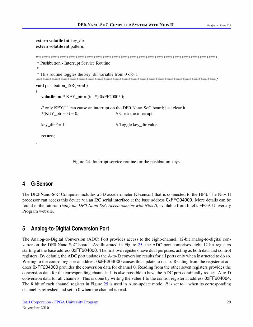
The Analog-to-Digital Conversion (ADC) Port provides access to the eight-channel, 12-bit analog-to-digital con-verter on the DE0-Nano-SoC board. As illustrated in Figure 25, the ADC port comprises eight 12-bit registersstarting at the base address 0xFF204000. The first two registers have dual purposes, acting as both data and controlregisters. By default, the ADC port updates the A-to-D conversion results for all ports only when instructed to do so.Writing to the control register at address 0xFF204000 causes this update to occur. Reading from the register at ad-dress 0xFF204000 provides the conversion data for channel 0. Reading from the other seven registers provides theconversion data for the corresponding channels. It is also possible to have the ADC port continually request A-to-Dconversion data for all channels. This is done by writing the value 1 to the control register at address 0xFF204004.The R bit of each channel register in Figure 25 is used in Auto-update mode. R is set to 1 when its correspondingchannel is refreshed and set to 0 when the channel is read.
Intel Corporation - FPGA University ProgramNovember 2016
29
DE0-NANO-SOC COMPUTER SYSTEM WITH NIOS II For Quartus Prime 16.1
Address 031 . . .
0xFF204000
0xFF20401C
0xFF204004
Unused Channel 0 / Update
Channel 7
Channel 1 / Auto-update
... not shown
12 . . .
0xFF204008 Channel 2
11
Unused
Unused
Unused
Figure 25. ADC port registers.
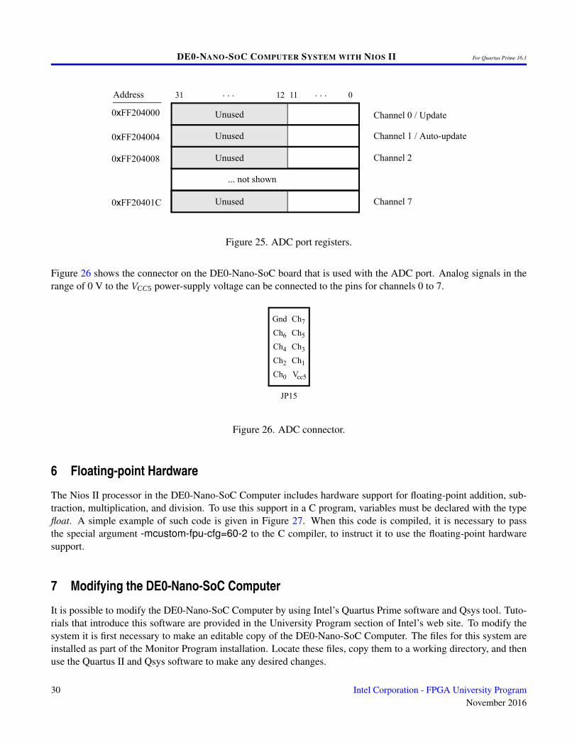
Figure 26 shows the connector on the DE0-Nano-SoC board that is used with the ADC port. Analog signals in therange of 0 V to the VCC 5 power-supply voltage can be connected to the pins for channels 0 to 7.
Gnd Ch7Ch6 Ch5Ch4 Ch3Ch2 Ch1Ch0 V
JP15
cc5
Figure 26. ADC connector.
6 Floating-point Hardware
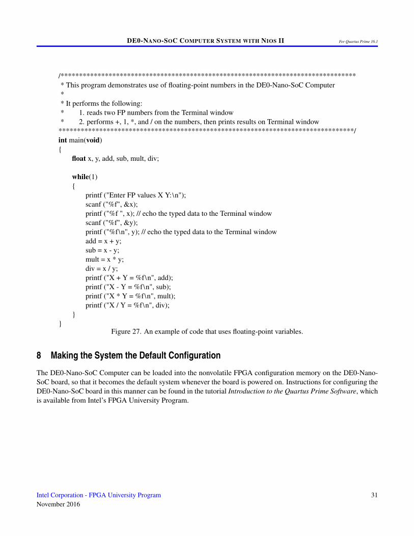
The Nios II processor in the DE0-Nano-SoC Computer includes hardware support for floating-point addition, sub-traction, multiplication, and division. To use this support in a C program, variables must be declared with the typefloat. A simple example of such code is given in Figure 27. When this code is compiled, it is necessary to passthe special argument -mcustom-fpu-cfg=60-2 to the C compiler, to instruct it to use the floating-point hardwaresupport.
7 Modifying the DE0-Nano-SoC Computer
It is possible to modify the DE0-Nano-SoC Computer by using Intel’s Quartus Prime software and Qsys tool. Tuto-rials that introduce this software are provided in the University Program section of Intel’s web site. To modify thesystem it is first necessary to make an editable copy of the DE0-Nano-SoC Computer. The files for this system areinstalled as part of the Monitor Program installation. Locate these files, copy them to a working directory, and thenuse the Quartus II and Qsys software to make any desired changes.
30 Intel Corporation - FPGA University ProgramNovember 2016
DE0-NANO-SOC COMPUTER SYSTEM WITH NIOS II For Quartus Prime 16.1
/********************************************************************************* This program demonstrates use of floating-point numbers in the DE0-Nano-SoC Computer** It performs the following:* 1. reads two FP numbers from the Terminal window* 2. performs +, 1, *, and / on the numbers, then prints results on Terminal window
********************************************************************************/int main(void){
float x, y, add, sub, mult, div;
while(1){
printf ("Enter FP values X Y:\n");scanf ("%f", &x);printf ("%f ", x); // echo the typed data to the Terminal windowscanf ("%f", &y);printf ("%f\n", y); // echo the typed data to the Terminal windowadd = x + y;sub = x - y;mult = x * y;div = x / y;printf ("X + Y = %f\n", add);printf ("X - Y = %f\n", sub);printf ("X * Y = %f\n", mult);printf ("X / Y = %f\n", div);
}}
Figure 27. An example of code that uses floating-point variables.
8 Making the System the Default Configuration
The DE0-Nano-SoC Computer can be loaded into the nonvolatile FPGA configuration memory on the DE0-Nano-SoC board, so that it becomes the default system whenever the board is powered on. Instructions for configuring theDE0-Nano-SoC board in this manner can be found in the tutorial Introduction to the Quartus Prime Software, whichis available from Intel’s FPGA University Program.
Intel Corporation - FPGA University ProgramNovember 2016
31
DE0-NANO-SOC COMPUTER SYSTEM WITH NIOS II For Quartus Prime 16.1
9 Memory Layout
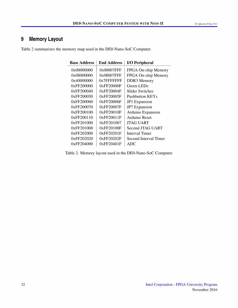
Table 2 summarizes the memory map used in the DE0-Nano-SoC Computer.
Base Address End Address I/O Peripheral
0x00000000 0x00007FFF FPGA On-chip Memory0x08000000 0x08007FFF FPGA On-chip Memory0x40000000 0x7FFFFFFF DDR3 Memory0xFF200000 0xFF20000F Green LEDs0xFF200040 0xFF20004F Slider Switches0xFF200050 0xFF20005F Pushbutton KEYs0xFF200060 0xFF20006F JP1 Expansion0xFF200070 0xFF20007F JP7 Expansion0xFF200100 0xFF20010F Arduino Expansion0xFF200110 0xFF20011F Arduino Reset0xFF201000 0xFF201007 JTAG UART0xFF201008 0xFF20100F Second JTAG UART0xFF202000 0xFF20201F Interval Timer0xFF202020 0xFF20202F Second Interval Timer0xFF204000 0xFF20401F ADC
Table 2. Memory layout used in the DE0-Nano-SoC Computer.
32 Intel Corporation - FPGA University ProgramNovember 2016
DE0-NANO-SOC COMPUTER SYSTEM WITH NIOS II For Quartus Prime 16.1
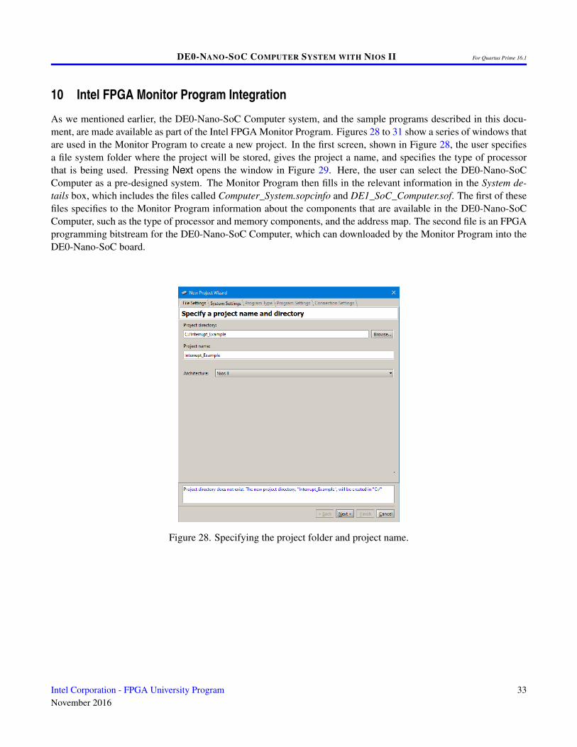
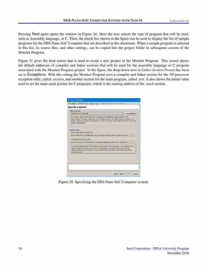
10 Intel FPGA Monitor Program Integration
As we mentioned earlier, the DE0-Nano-SoC Computer system, and the sample programs described in this docu-ment, are made available as part of the Intel FPGA Monitor Program. Figures 28 to 31 show a series of windows thatare used in the Monitor Program to create a new project. In the first screen, shown in Figure 28, the user specifiesa file system folder where the project will be stored, gives the project a name, and specifies the type of processorthat is being used. Pressing Next opens the window in Figure 29. Here, the user can select the DE0-Nano-SoCComputer as a pre-designed system. The Monitor Program then fills in the relevant information in the System de-tails box, which includes the files called Computer_System.sopcinfo and DE1_SoC_Computer.sof. The first of thesefiles specifies to the Monitor Program information about the components that are available in the DE0-Nano-SoCComputer, such as the type of processor and memory components, and the address map. The second file is an FPGAprogramming bitstream for the DE0-Nano-SoC Computer, which can downloaded by the Monitor Program into theDE0-Nano-SoC board.
Figure 28. Specifying the project folder and project name.
Intel Corporation - FPGA University ProgramNovember 2016
33
DE0-NANO-SOC COMPUTER SYSTEM WITH NIOS II For Quartus Prime 16.1
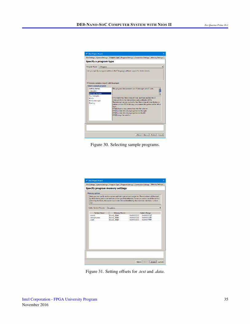
Pressing Next again opens the window in Figure 30. Here the user selects the type of program that will be used,such as Assembly language, or C. Then, the check box shown in the figure can be used to display the list of sampleprograms for the DE0-Nano-SoC Computer that are described in this document. When a sample program is selectedin this list, its source files, and other settings, can be copied into the project folder in subsequent screens of theMonitor Program.
Figure 31 gives the final screen that is used to create a new project in the Monitor Program. This screen showsthe default addresses of compiler and linker sections that will be used for the assembly language or C programassociated with the Monitor Program project. In the figure, the drop-down next to Linker Section Presets has beenset to Exceptions. With this setting the Monitor Program uses a compiler and linker section for the A9 processorexception table, called .vectors, and another section for the main program, called .text. It also shows the initial valueused to set the main stack pointer for C programs, which is the starting address of the .stack section.
Figure 29. Specifying the DE0-Nano-SoC Computer system.
34 Intel Corporation - FPGA University ProgramNovember 2016
DE0-NANO-SOC COMPUTER SYSTEM WITH NIOS II For Quartus Prime 16.1
Figure 30. Selecting sample programs.
Figure 31. Setting offsets for .text and .data.
Intel Corporation - FPGA University ProgramNovember 2016
35
DE0-NANO-SOC COMPUTER SYSTEM WITH NIOS II For Quartus Prime 16.1
Copyright © 1991-2016 Intel Corporation. All rights reserved. Intel, The Programmable Solutions Company, thestylized Intel logo, specific device designations, and all other words and logos that are identified as trademarksand/or service marks are, unless noted otherwise, the trademarks and service marks of Intel Corporation in the U.S.and other countries. All other product or service names are the property of their respective holders. Intel productsare protected under numerous U.S. and foreign patents and pending applications, mask work rights, and copyrights.Intel warrants performance of its semiconductor products to current specifications in accordance with Intel’s stan-dard warranty, but reserves the right to make changes to any products and services at any time without notice. Intelassumes no responsibility or liability arising out of the application or use of any information, product, or servicedescribed herein except as expressly agreed to in writing by Intel Corporation. Intel customers are advised to obtainthe latest version of device specifications before relying on any published information and before placing orders forproducts or services.
This document is being provided on an “as-is” basis and as an accommodation and therefore all warranties, repre-sentations or guarantees of any kind (whether express, implied or statutory) including, without limitation, warrantiesof merchantability, non-infringement, or fitness for a particular purpose, are specifically disclaimed.
36 Intel Corporation - FPGA University ProgramNovember 2016