
Computer System for the Altera DE0-Nano Board … · for the Altera DE0-Nano ... DE0-Nano Computer...
39
Computer System for the Altera DE0-Nano Board For Quartus II 13.0 1 Introduction This document describes a computer system that can be implemented on the Altera DE0-Nano development and education board. This system, called the DE0-Nano Computer, is intended to be used as a platform for experiments in computer organization and embedded systems. To support these beginning experiments, the system contains a processor, memory, an analog-to-digital converter, an accelerometer and some simple I/O peripherals. The FPGA programming file that implements this system, as well as its design source files, can be obtained from the University Program section of Altera’s web site. 2 DE0-Nano Computer Contents A block diagram of the DE0-Nano Computer is shown in Figure 1. Its main components include the Altera Nios II processor, memory for program and data storage, parallel ports connected to switches and lights, and a timer module. Additionally, the DE0-Nano Computer supports the onboard analog-to-digital converter and the accelerometer. As shown in the figure, the processor and its interfaces to I/O devices are implemented inside the Cyclone R IV FPGA chip on the DE0-Nano board. Each of the components shown in Figure 1 is described below. 2.1 Nios II Processor The Altera Nios R II processor is a 32-bit CPU that can be instantiated in an Altera FPGA chip. Three versions of the Nios II processor are available, designated economy (/e), standard (/s), and fast (/f). The DE0-Nano Computer includes the Nios II/s version, which has an appropriate feature set for use in introductory experiments. The Nios II processor is configured to include floating-point hardware support, which is described in section An overview of the Nios II processor can be found in the document Introduction to the Altera Nios II Processor, which is provided in the University Program section of Altera’s web site. An easy way to begin working with the DE0-Nano Computer and the Nios II processor is to make use of a utility called the Altera Monitor Program. This utility provides an easy way to assemble and compile Nios II programs on the DE0-Nano Computer that are written in either assembly language or the C programming language. The Monitor Program, which can be downloaded from Altera’s web site, is an application program that runs on the host computer connected to the DE0-Nano board. The Monitor Program can be used to control the execution of code on Nios II, list (and edit) the contents of processor registers, display/edit the contents of memory on the DE0-Nano board, and similar operations. The Monitor Program includes the DE0-Nano Computer as a predesigned system that can be downloaded onto the DE0-Nano board, as well as several sample programs in assembly language and C that show how to use various peripheral devices in the DE0-Nano Computer. Some images that show how the DE0-Nano Computer is integrated with the Monitor Program are described in section 7. An overview of the Monitor Program is available in the document Altera Monitor Program Altera Corporation - University Program May 2013 1
Transcript of Computer System for the Altera DE0-Nano Board … · for the Altera DE0-Nano ... DE0-Nano Computer...
Computer Systemfor the Altera DE0-Nano Board
For Quartus II 13.0
1 Introduction
This document describes a computer system that can be implemented on the Altera DE0-Nano development andeducation board. This system, called the DE0-Nano Computer, is intended to be used as a platform for experimentsin computer organization and embedded systems. To support these beginning experiments, the system contains aprocessor, memory, an analog-to-digital converter, an accelerometer and some simple I/O peripherals. The FPGAprogramming file that implements this system, as well as its design source files, can be obtained from the UniversityProgram section of Altera’s web site.
2 DE0-Nano Computer Contents
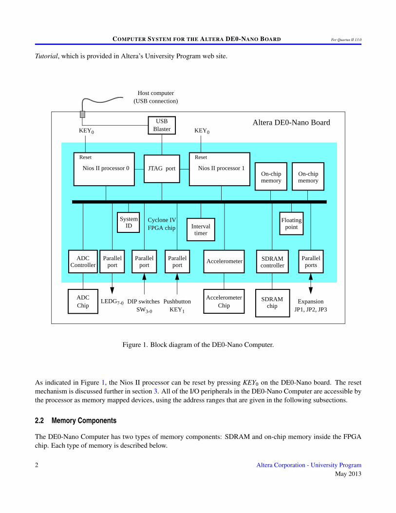
A block diagram of the DE0-Nano Computer is shown in Figure 1. Its main components include the Altera Nios IIprocessor, memory for program and data storage, parallel ports connected to switches and lights, and a timer module.Additionally, the DE0-Nano Computer supports the onboard analog-to-digital converter and the accelerometer. Asshown in the figure, the processor and its interfaces to I/O devices are implemented inside the Cyclone R©IV FPGAchip on the DE0-Nano board. Each of the components shown in Figure 1 is described below.
2.1 Nios II Processor
The Altera Nios R©II processor is a 32-bit CPU that can be instantiated in an Altera FPGA chip. Three versions ofthe Nios II processor are available, designated economy (/e), standard (/s), and fast (/f). The DE0-Nano Computerincludes the Nios II/s version, which has an appropriate feature set for use in introductory experiments. The Nios IIprocessor is configured to include floating-point hardware support, which is described in section
An overview of the Nios II processor can be found in the document Introduction to the Altera Nios II Processor,which is provided in the University Program section of Altera’s web site. An easy way to begin working with theDE0-Nano Computer and the Nios II processor is to make use of a utility called the Altera Monitor Program. Thisutility provides an easy way to assemble and compile Nios II programs on the DE0-Nano Computer that are writtenin either assembly language or the C programming language. The Monitor Program, which can be downloaded fromAltera’s web site, is an application program that runs on the host computer connected to the DE0-Nano board. TheMonitor Program can be used to control the execution of code on Nios II, list (and edit) the contents of processorregisters, display/edit the contents of memory on the DE0-Nano board, and similar operations. The Monitor Programincludes the DE0-Nano Computer as a predesigned system that can be downloaded onto the DE0-Nano board, aswell as several sample programs in assembly language and C that show how to use various peripheral devices in theDE0-Nano Computer. Some images that show how the DE0-Nano Computer is integrated with the Monitor Programare described in section 7. An overview of the Monitor Program is available in the document Altera Monitor Program
Altera Corporation - University ProgramMay 2013
1
COMPUTER SYSTEM FOR THE ALTERA DE0-NANO BOARD For Quartus II 13.0
Tutorial, which is provided in Altera’s University Program web site.
DIP switches SW3-0
JTAG port
LEDG7-0
On-chipmemory
ExpansionJP1, JP2, JP3
System
Host computer(USB connection)
USBBlaster
Altera DE0-Nano Board
IDtimer
IntervalCyclone IVFPGA chip
Parallelports
Parallelport
Parallelport
PushbuttonKEY1
Parallelport
SDRAMchip
SDRAMcontroller
On-chipmemory
Nios II processor 1
Reset
KEY0
Nios II processor 0
Reset
KEY0
pointFloating
ADCController
Accelerometer
ADCChip
AccelerometerChip
Figure 1. Block diagram of the DE0-Nano Computer.
As indicated in Figure 1, the Nios II processor can be reset by pressing KEY0 on the DE0-Nano board. The resetmechanism is discussed further in section 3. All of the I/O peripherals in the DE0-Nano Computer are accessible bythe processor as memory mapped devices, using the address ranges that are given in the following subsections.
2.2 Memory Components
The DE0-Nano Computer has two types of memory components: SDRAM and on-chip memory inside the FPGAchip. Each type of memory is described below.
2 Altera Corporation - University ProgramMay 2013
COMPUTER SYSTEM FOR THE ALTERA DE0-NANO BOARD For Quartus II 13.0
2.2.1 SDRAM
An SDRAM Controller provides a 32-bit interface to the synchronous dynamic RAM (SDRAM) chip on the DE0-Nano board. This SDRAM chip is organized as 16M x 16 bits, but is accessible by the Nios II processor using word(32-bit), halfword (16-bit), or byte operations. The SDRAM memory is mapped to the address space 0x00000000to 0x01FFFFFF.
2.2.2 On-Chip Memory
The DE0-Nano Computer includes an 8-Kbyte memory that is implemented in the Cyclone IV FPGA chip. Thismemory is organized as 2K x 32 bits, and can be accessed using either word, halfword, or byte operations. Thememory spans addresses in the range 0x08000000 to 0x08001FFF.
2.2.3 On-Chip Memory
The DE0-Nano Computer includes a second 8-Kbyte memory implemented in the Cyclone IV FPGA chip. Thismemory is also organized as 2K x 32 bits, and can be accessed using either word, halfword, or byte operations. Itspans addresses in the range 0x09000000 to 0x09001FFF.
2.3 Parallel Ports
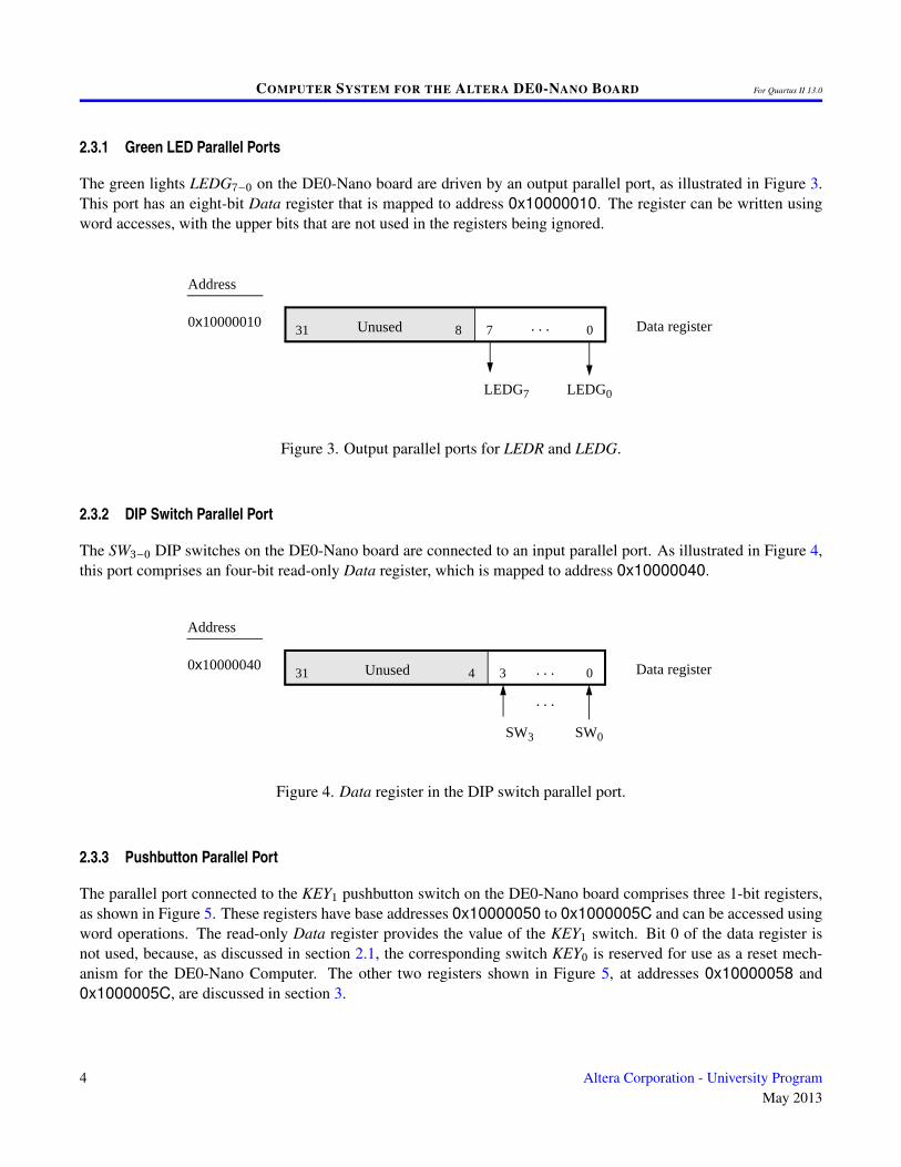
The DE0-Nano Computer includes several parallel ports that support input, output, and bidirectional transfers of databetween the Nios II processor and I/O peripherals. As illustrated in Figure 2, each parallel port is assigned a Baseaddress and contains up to four 32-bit registers. Ports that have output capability include a writable Data register,and ports with input capability have a readable Data register. Bidirectional parallel ports also include a Directionregister that has the same bit-width as the Data register. Each bit in the Data register can be configured as an inputby setting the corresponding bit in the Direction register to 0, or as an output by setting this bit position to 1. TheDirection register is assigned the address Base + 4.
Address 02 14 331 30 . . .
Base
Base + 8
Base + C
Base + 4
Input or output data bits
Direction bits
Edge bits
Mask bits
Data register
Direction register
Interruptmask register
Edgecapture register
Direction bits
Figure 2. Parallel port registers in the DE0-Nano Computer.
Some of the parallel ports in the DE0-Nano Computer have registers at addresses Base + 8 and Base + C, as indicatedin Figure 2. These registers are discussed in section 3.
Altera Corporation - University ProgramMay 2013
3
COMPUTER SYSTEM FOR THE ALTERA DE0-NANO BOARD For Quartus II 13.0
2.3.1 Green LED Parallel Ports
The green lights LEDG7−0 on the DE0-Nano board are driven by an output parallel port, as illustrated in Figure 3.This port has an eight-bit Data register that is mapped to address 0x10000010. The register can be written usingword accesses, with the upper bits that are not used in the registers being ignored.
0x10000010
LEDG0LEDG7
Address
031 78 . . .Unused Data register
Figure 3. Output parallel ports for LEDR and LEDG.
2.3.2 DIP Switch Parallel Port
The SW3−0 DIP switches on the DE0-Nano board are connected to an input parallel port. As illustrated in Figure 4,this port comprises an four-bit read-only Data register, which is mapped to address 0x10000040.
0x10000040
SW0SW3
Address
031 34 . . .Unused Data register
. . .
Figure 4. Data register in the DIP switch parallel port.
2.3.3 Pushbutton Parallel Port
The parallel port connected to the KEY1 pushbutton switch on the DE0-Nano board comprises three 1-bit registers,as shown in Figure 5. These registers have base addresses 0x10000050 to 0x1000005C and can be accessed usingword operations. The read-only Data register provides the value of the KEY1 switch. Bit 0 of the data register isnot used, because, as discussed in section 2.1, the corresponding switch KEY0 is reserved for use as a reset mech-anism for the DE0-Nano Computer. The other two registers shown in Figure 5, at addresses 0x10000058 and0x1000005C, are discussed in section 3.
4 Altera Corporation - University ProgramMay 2013
COMPUTER SYSTEM FOR THE ALTERA DE0-NANO BOARD For Quartus II 13.0
Address 01231 30 . . .
0x10000050
0x10000058
0x1000005C
Unused
KEY1
Edge bits
Mask bits
Unused
Unused
Unused
Data register
Interruptmask register
Edgecapture register
Unused
Figure 5. Registers used in the pushbutton parallel port.
2.3.4 Expansion Parallel Ports JP1 and JP2
The DE0-Nano Computer includes two bidirectional parallel ports that are connected to the JP1 and JP2 expan-sion headers on the DE0-Nano board. Each of these parallel ports includes the four 32-bit registers that weredescribed previously for Figure 2. The base addresses of the ports connected to JP1 and JP2 are 0x10000060 and0x10000070, respectively. Figure 6 gives a diagram of the JP1 and JP2 expansion connectors on the DE0-Nanoboard, and shows how the respective parallel port Data register bits, D31−0, are assigned to the pins on the connector.The figure shows that bit D0 of the parallel port for JP1 is assigned to the pin at the top right corner of the connector,bit D1 is assigned below this, and so on. Note that some of the pins on JP1 and JP2 are not usable as input/outputconnections, and are therefore not used by the parallel ports. Also, only 32 of the 36 data pins that appear on eachconnector can be used.
2.3.5 Expansion Parallel Ports JP3
The DE0-Nano Computer includes two parallel ports that are connected to the JP3 expansion header on the DE0-Nano board. One of these parallel ports provides 13 bidirectional connections, and the other port provides threeinput-only connections. Each of the parallel ports includes the four 32-bit registers that were described previouslyfor Figure 2. The base address of the 13-bit bidirectional port connected to JP3 is 0x10000080 and the base addressof the input-only port is 0x10000090. Figure 7 gives a diagram of the JP3 expansion connector on the DE0-Nanoboard, and shows how both the bidirectional and input-only parallel ports are connected. The figure shows that bitsD0 to D12 of the bidirectional parallel port are assigned to pins 5 to 17 of the JP3 connector. Bits IN0 to IN2 of theinput-only parallel port are assigned to pins 2 to 4 of the connector.
2.3.6 Using the Parallel Ports with Assembly Language Code and C Code
The DE0-Nano Computer provides a convenient platform for experimenting with Nios II assembly language code, orC code. A simple example of such code is provided in Figures 8 and 9. Both programs perform the same operations,and illustrate the use of parallel ports by using either assembly language or C code.
The code in the figures displays a rotating pattern on the green LEDG lights. This pattern is shifted to the right byusing a Nios II rotate instruction, and a delay loop is used to make the shifting slow enough to observe. The patternon the LEDG lights can be changed using the settings on the SW DIP switches on the DE0-Nano board by pressingpushbutton KEY1 (recall from section 2.1 that KEY0 causes a reset of the DE0-Nano Computer). When a pushbutton
Altera Corporation - University ProgramMay 2013
5
COMPUTER SYSTEM FOR THE ALTERA DE0-NANO BOARD For Quartus II 13.0
D0D1
D2 D3D4 D5D6 D7Unused
D10 D11D12 D13
D14D15
D16 D17D18 D19
D22 D23D24 D25D26 D27D28 D29D30 D31
Unused
JP1 JP2
Pin 1 Pin 1
Pin 40 Pin 40
D8 D9
D20 D21
D0D1
D2 D3D4 D5D6 D7Unused
D10 D11D12 D13
D14D15
D16 D17D18 D19
D22 D23D24 D25D26 D27D28 D29D30 D31
Unused
D8 D9
D20 D21
Figure 6. Assignment of parallel port bits to pins on JP1 and JP2.
D0 D1D2 D3D4 D5
D8 D9D10 D11D12
JP3
Pin 1
Pin 26
D6 D7
IN1 IN2
IN0
Figure 7. Assignment of parallel port bits to pins on JP3.
key is pressed, the program waits in a loop until the key is released.
The source code files shown in Figures 8 and 9 are distributed as part of the Altera Monitor Program. The files canbe found under the heading sample programs, and are identified by the name Getting Started.
6 Altera Corporation - University ProgramMay 2013
COMPUTER SYSTEM FOR THE ALTERA DE0-NANO BOARD For Quartus II 13.0
/********************************************************************************* This program demonstrates use of parallel ports in the DE0-Nano Computer* It performs the following:* 1. displays a rotating pattern on the green LEDG* 2. if KEY[1] is pressed, uses the SW switches as the pattern
********************************************************************************/.text /* executable code follows */.global _start
_start:/* initialize base addresses of parallel ports */movia r16, 0x10000010 /* green LED base address */movia r15, 0x10000040 /* SW slider switch (DIP switches) base address */movia r17, 0x10000050 /* pushbutton KEY base address */movia r19, LEDG_bitsldw r6, 0(r19) /* load pattern for LEDG lights */
DO_DISPLAY:ldwio r4, 0(r15) /* load slider (DIP) switches */ldwio r5, 0(r17) /* load pushbuttons */beq r5, r0, NO_BUTTONmov r6, r4 /* use SW (DIP switch) values on LEDG */roli r4, r4, 8or r6, r6, r4roli r4, r4, 8or r6, r6, r4roli r4, r4, 8or r6, r6, r4
WAIT:ldwio r5, 0(r17) /* load pushbuttons */bne r5, r0, WAIT /* wait for button release */
NO_BUTTON:stwio r6, 0(r16) /* store to LEDG */roli r6, r6, 1 /* rotate the displayed pattern */movia r7, 150000 /* delay counter */
DELAY:subi r7, r7, 1bne r7, r0, DELAYbr DO_DISPLAY
.data /* data follows */LEDG_bits:
.word 0x0F0F0F0F
.endFigure 8. An example of Nios II assembly language code that uses parallel ports.
Altera Corporation - University ProgramMay 2013
7
COMPUTER SYSTEM FOR THE ALTERA DE0-NANO BOARD For Quartus II 13.0
/********************************************************************************* This program demonstrates use of parallel ports in the DE0-Nano Computer* It performs the following:* 1. displays a rotating pattern on the green LEDG* 2. if KEY[1] is pressed, uses the SW switches as the pattern
********************************************************************************/int main(void){
/* Declare volatile pointers to I/O registers (volatile means that IO load and storeinstructions (e.g., ldwio, stwio) will be used to access these pointer locations) */
volatile int * green_LED_ptr = (int *) 0x10000010; // green LED addressvolatile int * SW_switch_ptr = (int *) 0x10000040; // SW DIP switch addressvolatile int * KEY_ptr = (int *) 0x10000050; // pushbutton KEY address
int LEDG_bits = 0x0F0F0F0F; // pattern for LEDG lightsint SW_value, KEY_value;volatile int delay_count; // volatile so C compile does not remove loop
while(1){
SW_value = *(SW_switch_ptr); // read the SW DIP switch values
KEY_value = *(KEY_ptr); // read the pushbutton KEY valuesif (KEY_value != 0) // check if any KEY was pressed{
/* set pattern using SW values */LEDG_bits = SW_value | (SW_value << 8) | (SW_value << 16) | (SW_value << 24);while (*KEY_ptr); // wait for pushbutton KEY release
}*(green_LED_ptr) = LEDG_bits; // light up the green LEDs
/* rotate the pattern shown on the LEDs */if (LEDG_bits & 0x80000000)
LEDG_bits = (LEDG_bits << 1) | 1;else
LEDG_bits = LEDG_bits << 1;
for (delay_count = 150000; delay_count != 0; --delay_count); // delay loop}
}
Figure 9. An example of C code that uses parallel ports.
8 Altera Corporation - University ProgramMay 2013
COMPUTER SYSTEM FOR THE ALTERA DE0-NANO BOARD For Quartus II 13.0
2.4 JTAG Port
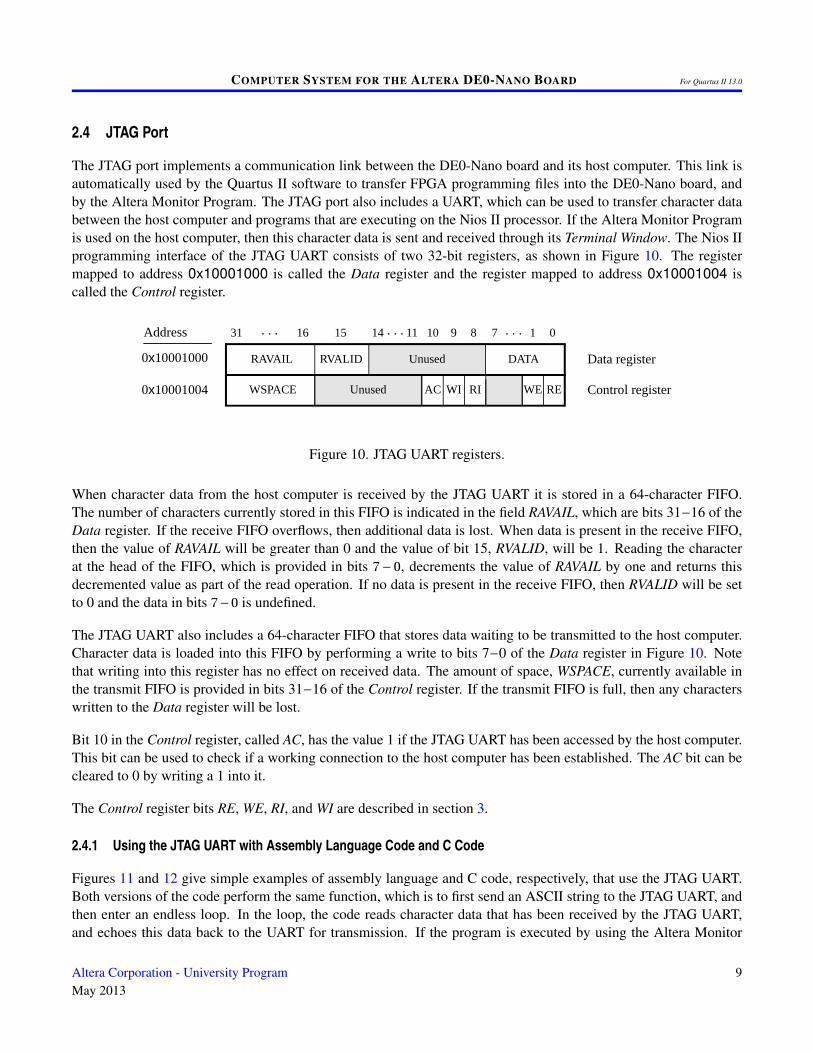
The JTAG port implements a communication link between the DE0-Nano board and its host computer. This link isautomatically used by the Quartus II software to transfer FPGA programming files into the DE0-Nano board, andby the Altera Monitor Program. The JTAG port also includes a UART, which can be used to transfer character databetween the host computer and programs that are executing on the Nios II processor. If the Altera Monitor Programis used on the host computer, then this character data is sent and received through its Terminal Window. The Nios IIprogramming interface of the JTAG UART consists of two 32-bit registers, as shown in Figure 10. The registermapped to address 0x10001000 is called the Data register and the register mapped to address 0x10001004 iscalled the Control register.
Address 0731 16. . .
0x10001000
0x10001004
DATARAVAIL
14 8. . . . . .
WSPACE Unused WI RI WE RE
1
RVALID
AC
10 911
Unused
15
Data register
Control register
Figure 10. JTAG UART registers.
When character data from the host computer is received by the JTAG UART it is stored in a 64-character FIFO.The number of characters currently stored in this FIFO is indicated in the field RAVAIL, which are bits 31−16 of theData register. If the receive FIFO overflows, then additional data is lost. When data is present in the receive FIFO,then the value of RAVAIL will be greater than 0 and the value of bit 15, RVALID, will be 1. Reading the characterat the head of the FIFO, which is provided in bits 7−0, decrements the value of RAVAIL by one and returns thisdecremented value as part of the read operation. If no data is present in the receive FIFO, then RVALID will be setto 0 and the data in bits 7−0 is undefined.
The JTAG UART also includes a 64-character FIFO that stores data waiting to be transmitted to the host computer.Character data is loaded into this FIFO by performing a write to bits 7−0 of the Data register in Figure 10. Notethat writing into this register has no effect on received data. The amount of space, WSPACE, currently available inthe transmit FIFO is provided in bits 31−16 of the Control register. If the transmit FIFO is full, then any characterswritten to the Data register will be lost.
Bit 10 in the Control register, called AC, has the value 1 if the JTAG UART has been accessed by the host computer.This bit can be used to check if a working connection to the host computer has been established. The AC bit can becleared to 0 by writing a 1 into it.
The Control register bits RE, WE, RI, and WI are described in section 3.
2.4.1 Using the JTAG UART with Assembly Language Code and C Code
Figures 11 and 12 give simple examples of assembly language and C code, respectively, that use the JTAG UART.Both versions of the code perform the same function, which is to first send an ASCII string to the JTAG UART, andthen enter an endless loop. In the loop, the code reads character data that has been received by the JTAG UART,and echoes this data back to the UART for transmission. If the program is executed by using the Altera Monitor
Altera Corporation - University ProgramMay 2013
9
COMPUTER SYSTEM FOR THE ALTERA DE0-NANO BOARD For Quartus II 13.0
Program, then any keyboard character that is typed into the Terminal Window of the Monitor Program will be echoedback, causing the character to appear in the Terminal Window.
The source code files shown in Figures 11 and 12 are made available as part of the Altera Monitor Program. Thefiles can be found under the heading sample programs, and are identified by the name JTAG UART.
/********************************************************************************* This program demonstrates use of the JTAG UART port in the DE0-Nano Computer** It performs the following:* 1. sends a text string to the JTAG UART* 2. reads character data from the JTAG UART* 3. echos the character data back to the JTAG UART
********************************************************************************/.text /* executable code follows */.global _start
_start:/* set up stack pointer */movia sp, 0x01FFFFFC /* stack starts from highest memory address in SDRAM */
movia r6, 0x10001000 /* JTAG UART base address */
/* print a text string */movia r8, TEXT_STRING
LOOP:ldb r5, 0(r8)beq r5, zero, GET_JTAG /* string is null-terminated */call PUT_JTAGaddi r8, r8, 1br LOOP
/* read and echo characters */GET_JTAG:
ldwio r4, 0(r6) /* read the JTAG UART data register */andi r8, r4, 0x8000 /* check if there is new data */beq r8, r0, GET_JTAG /* if no data, wait */andi r5, r4, 0x00ff /* the data is in the least significant byte */
call PUT_JTAG /* echo character */br GET_JTAG.end
Figure 11. An example of assembly language code that uses the JTAG UART (Part a).
10 Altera Corporation - University ProgramMay 2013
COMPUTER SYSTEM FOR THE ALTERA DE0-NANO BOARD For Quartus II 13.0
/********************************************************************************* Subroutine to send a character to the JTAG UART* r5 = character to send* r6 = JTAG UART base address
********************************************************************************/.global PUT_JTAG
PUT_JTAG:/* save any modified registers */subi sp, sp, 4 /* reserve space on the stack */stw r4, 0(sp) /* save register */
ldwio r4, 4(r6) /* read the JTAG UART Control register */andhi r4, r4, 0xffff /* check for write space */beq r4, r0, END_PUT /* if no space, ignore the character */stwio r5, 0(r6) /* send the character */
END_PUT:/* restore registers */ldw r4, 0(sp)addi sp, sp, 4
ret
.data /* data follows */TEXT_STRING:
.asciz "\nJTAG UART example code\n> "
.end
Figure 11. An example of assembly language code that uses the JTAG UART (Part b).
Altera Corporation - University ProgramMay 2013
11
COMPUTER SYSTEM FOR THE ALTERA DE0-NANO BOARD For Quartus II 13.0
void put_jtag(volatile int *, char); // function prototype
/********************************************************************************* This program demonstrates use of the JTAG UART port in the DE0-Nano Computer** It performs the following:* 1. sends a text string to the JTAG UART* 2. reads character data from the JTAG UART* 3. echos the character data back to the JTAG UART
********************************************************************************/int main(void){
/* Declare volatile pointers to I/O registers (volatile means that IO load and storeinstructions (e.g., ldwio, stwio) will be used to access these pointer locations) */
volatile int * JTAG_UART_ptr = (int *) 0x10001000; // JTAG UART addressint data, i;char text_string[] = "\nJTAG UART example code\n> \0";
for (i = 0; text_string[i] != 0; ++i) // print a text stringput_jtag (JTAG_UART_ptr, text_string[i]);
/* read and echo characters */while(1){
data = *(JTAG_UART_ptr); // read the JTAG_UART data registerif (data & 0x00008000) // check RVALID to see if there is new data{
data = data & 0x000000FF; // the data is in the least significant byte/* echo the character */put_jtag (JTAG_UART_ptr, (char) data & 0xFF );
}}
}/********************************************************************************* Subroutine to send a character to the JTAG UART
********************************************************************************/void put_jtag( volatile int * JTAG_UART_ptr, char c ){
int control;control = *(JTAG_UART_ptr + 1); // read the JTAG_UART Control registerif (control & 0xFFFF0000) // if space, then echo character, else ignore
*(JTAG_UART_ptr) = c;}
Figure 12. An example of C code that uses the JTAG UART.
12 Altera Corporation - University ProgramMay 2013
COMPUTER SYSTEM FOR THE ALTERA DE0-NANO BOARD For Quartus II 13.0
2.5 Analog-to-Digital Converter
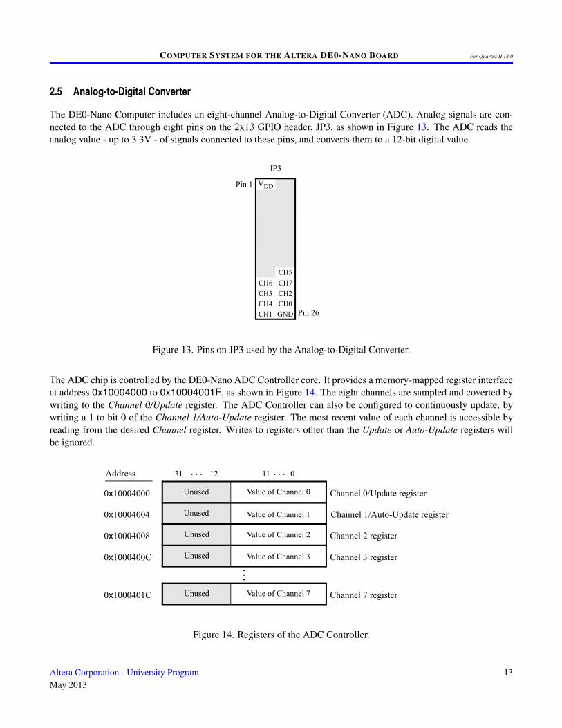
The DE0-Nano Computer includes an eight-channel Analog-to-Digital Converter (ADC). Analog signals are con-nected to the ADC through eight pins on the 2x13 GPIO header, JP3, as shown in Figure 13. The ADC reads theanalog value - up to 3.3V - of signals connected to these pins, and converts them to a 12-bit digital value.
CH5
JP3
Pin 1
Pin 26
CH7
CH2
CH0
GND
CH6
CH3
CH4
CH1
VDD
Figure 13. Pins on JP3 used by the Analog-to-Digital Converter.
The ADC chip is controlled by the DE0-Nano ADC Controller core. It provides a memory-mapped register interfaceat address 0x10004000 to 0x10004001F, as shown in Figure 14. The eight channels are sampled and coverted bywriting to the Channel 0/Update register. The ADC Controller can also be configured to continuously update, bywriting a 1 to bit 0 of the Channel 1/Auto-Update register. The most recent value of each channel is accessible byreading from the desired Channel register. Writes to registers other than the Update or Auto-Update registers willbe ignored.
Unused
Unused
Unused
Address 1131
0x10004004
. . .
Unused
0
0x10004000 Channel 0/Update register
Channel 1/Auto-Update registerUnused
. . . 12
0x1000401C
0x1000400C
0x10004008 Channel 2 register
Channel 7 register
Channel 3 register
. . .
Value of Channel 0
Value of Channel 1
Value of Channel 2
Value of Channel 3
Value of Channel 7
Figure 14. Registers of the ADC Controller.
Altera Corporation - University ProgramMay 2013
13
COMPUTER SYSTEM FOR THE ALTERA DE0-NANO BOARD For Quartus II 13.0
2.6 Accelerometer
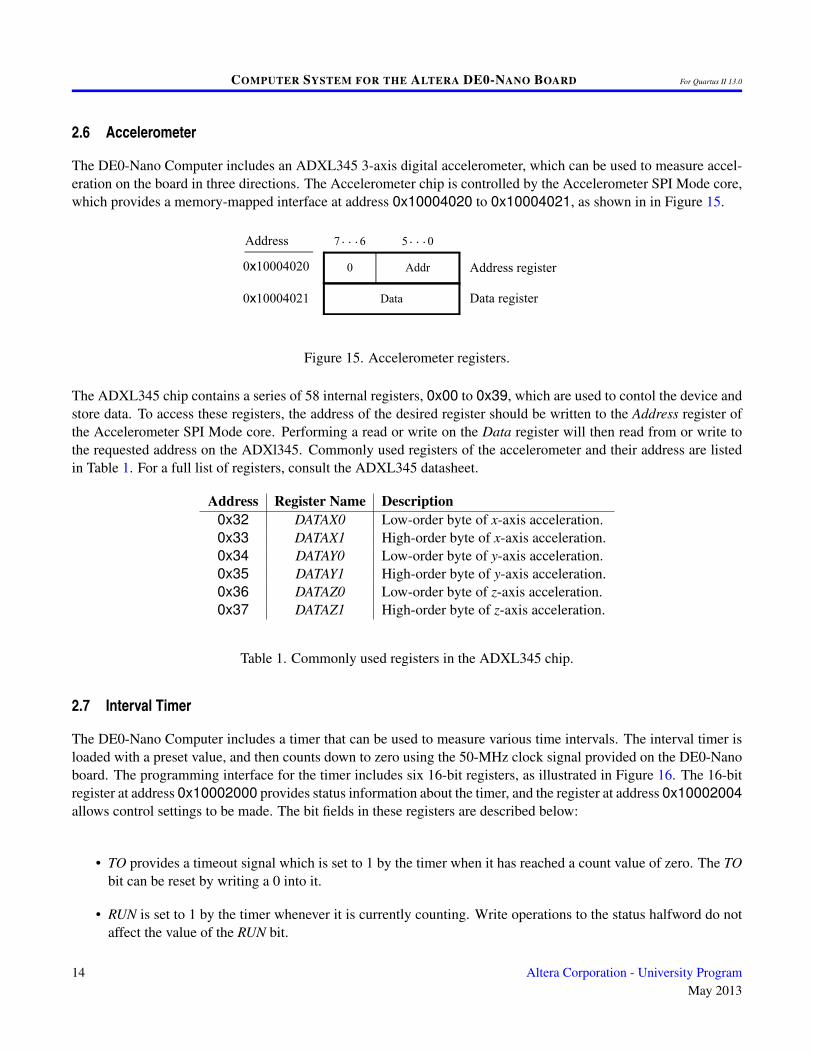
The DE0-Nano Computer includes an ADXL345 3-axis digital accelerometer, which can be used to measure accel-eration on the board in three directions. The Accelerometer chip is controlled by the Accelerometer SPI Mode core,which provides a memory-mapped interface at address 0x10004020 to 0x10004021, as shown in in Figure 15.
Address
0x10004021
0x10004020 Address register
Data register
7 6. . . 5 0. . .
0
Data
Addr
Figure 15. Accelerometer registers.
The ADXL345 chip contains a series of 58 internal registers, 0x00 to 0x39, which are used to contol the device andstore data. To access these registers, the address of the desired register should be written to the Address register ofthe Accelerometer SPI Mode core. Performing a read or write on the Data register will then read from or write tothe requested address on the ADXl345. Commonly used registers of the accelerometer and their address are listedin Table 1. For a full list of registers, consult the ADXL345 datasheet.
Address Register Name Description0x32 DATAX0 Low-order byte of x-axis acceleration.0x33 DATAX1 High-order byte of x-axis acceleration.0x34 DATAY0 Low-order byte of y-axis acceleration.0x35 DATAY1 High-order byte of y-axis acceleration.0x36 DATAZ0 Low-order byte of z-axis acceleration.0x37 DATAZ1 High-order byte of z-axis acceleration.
Table 1. Commonly used registers in the ADXL345 chip.
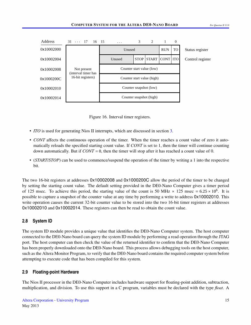
2.7 Interval Timer
The DE0-Nano Computer includes a timer that can be used to measure various time intervals. The interval timer isloaded with a preset value, and then counts down to zero using the 50-MHz clock signal provided on the DE0-Nanoboard. The programming interface for the timer includes six 16-bit registers, as illustrated in Figure 16. The 16-bitregister at address 0x10002000 provides status information about the timer, and the register at address 0x10002004allows control settings to be made. The bit fields in these registers are described below:
• TO provides a timeout signal which is set to 1 by the timer when it has reached a count value of zero. The TObit can be reset by writing a 0 into it.
• RUN is set to 1 by the timer whenever it is currently counting. Write operations to the status halfword do notaffect the value of the RUN bit.
14 Altera Corporation - University ProgramMay 2013
COMPUTER SYSTEM FOR THE ALTERA DE0-NANO BOARD For Quartus II 13.0
Address 01531 . . .
0x10002000
0x10002004
. . .
Unused RUN TO
1
START CONT ITOSTOP
16 217
Unused
Counter start value (low) 0x10002008
Counter start value (high)0x1000200C
Counter snapshot (low)0x10002010
Counter snapshot (high)0x10002014
3
Not present(interval timer has16-bit registers)
Status register
Control register
Figure 16. Interval timer registers.
• ITO is used for generating Nios II interrupts, which are discussed in section 3.
• CONT affects the continuous operation of the timer. When the timer reaches a count value of zero it auto-matically reloads the specified starting count value. If CONT is set to 1, then the timer will continue countingdown automatically. But if CONT = 0, then the timer will stop after it has reached a count value of 0.
• (START/STOP) can be used to commence/suspend the operation of the timer by writing a 1 into the respectivebit.
The two 16-bit registers at addresses 0x10002008 and 0x1000200C allow the period of the timer to be changedby setting the starting count value. The default setting provided in the DE0-Nano Computer gives a timer periodof 125 msec. To achieve this period, the starting value of the count is 50 MHz × 125 msec = 6.25× 10⁶. It ispossible to capture a snapshot of the counter value at any time by performing a write to address 0x10002010. Thiswrite operation causes the current 32-bit counter value to be stored into the two 16-bit timer registers at addresses0x10002010 and 0x10002014. These registers can then be read to obtain the count value.
2.8 System ID
The system ID module provides a unique value that identifies the DE0-Nano Computer system. The host computerconnected to the DE0-Nano board can query the system ID module by performing a read operation through the JTAGport. The host computer can then check the value of the returned identifier to confirm that the DE0-Nano Computerhas been properly downloaded onto the DE0-Nano board. This process allows debugging tools on the host computer,such as the Altera Monitor Program, to verify that the DE0-Nano board contains the required computer system beforeattempting to execute code that has been compiled for this system.
2.9 Floating-point Hardware
The Nios II processor in the DE0-Nano Computer includes hardware support for floating-point addition, subtraction,multiplication, and division. To use this support in a C program, variables must be declared with the type float. A
Altera Corporation - University ProgramMay 2013
15
COMPUTER SYSTEM FOR THE ALTERA DE0-NANO BOARD For Quartus II 13.0
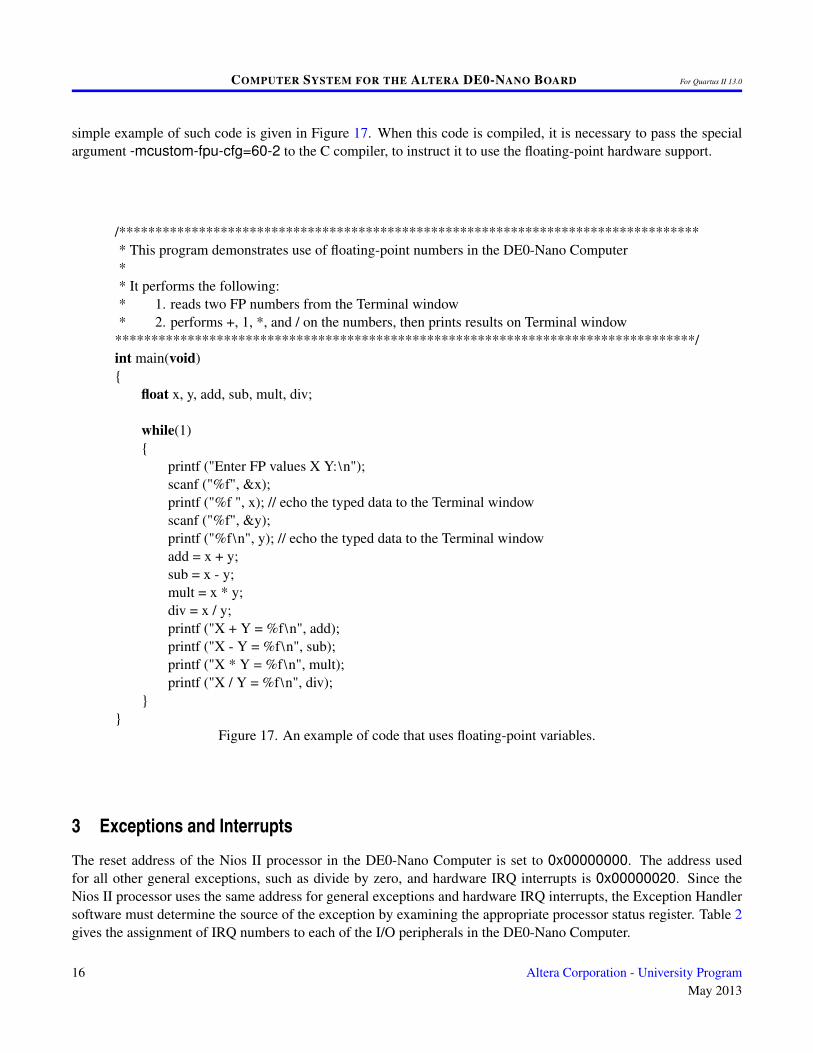
simple example of such code is given in Figure 17. When this code is compiled, it is necessary to pass the specialargument -mcustom-fpu-cfg=60-2 to the C compiler, to instruct it to use the floating-point hardware support.
/********************************************************************************* This program demonstrates use of floating-point numbers in the DE0-Nano Computer** It performs the following:* 1. reads two FP numbers from the Terminal window* 2. performs +, 1, *, and / on the numbers, then prints results on Terminal window
********************************************************************************/int main(void){
float x, y, add, sub, mult, div;
while(1){
printf ("Enter FP values X Y:\n");scanf ("%f", &x);printf ("%f ", x); // echo the typed data to the Terminal windowscanf ("%f", &y);printf ("%f\n", y); // echo the typed data to the Terminal windowadd = x + y;sub = x - y;mult = x * y;div = x / y;printf ("X + Y = %f\n", add);printf ("X - Y = %f\n", sub);printf ("X * Y = %f\n", mult);printf ("X / Y = %f\n", div);
}}
Figure 17. An example of code that uses floating-point variables.
3 Exceptions and Interrupts
The reset address of the Nios II processor in the DE0-Nano Computer is set to 0x00000000. The address usedfor all other general exceptions, such as divide by zero, and hardware IRQ interrupts is 0x00000020. Since theNios II processor uses the same address for general exceptions and hardware IRQ interrupts, the Exception Handlersoftware must determine the source of the exception by examining the appropriate processor status register. Table 2gives the assignment of IRQ numbers to each of the I/O peripherals in the DE0-Nano Computer.
16 Altera Corporation - University ProgramMay 2013
COMPUTER SYSTEM FOR THE ALTERA DE0-NANO BOARD For Quartus II 13.0
I/O Peripheral IRQ #Interval timer 0Pushbutton switch parallel port 1JTAG port 8JP1 Expansion parallel port 11JP2 Expansion parallel port 12JP3 Expansion parallel port (bidirectional) 13JP3 Expansion parallel port (input-only) 14Accelerometer 15
Table 2. Hardware IRQ interrupt assignment for the DE0-Nano Computer.
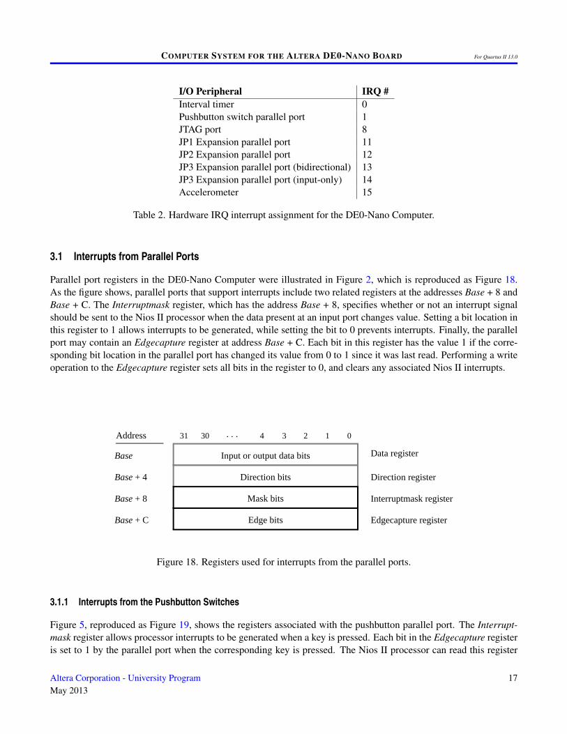
3.1 Interrupts from Parallel Ports
Parallel port registers in the DE0-Nano Computer were illustrated in Figure 2, which is reproduced as Figure 18.As the figure shows, parallel ports that support interrupts include two related registers at the addresses Base + 8 andBase + C. The Interruptmask register, which has the address Base + 8, specifies whether or not an interrupt signalshould be sent to the Nios II processor when the data present at an input port changes value. Setting a bit location inthis register to 1 allows interrupts to be generated, while setting the bit to 0 prevents interrupts. Finally, the parallelport may contain an Edgecapture register at address Base + C. Each bit in this register has the value 1 if the corre-sponding bit location in the parallel port has changed its value from 0 to 1 since it was last read. Performing a writeoperation to the Edgecapture register sets all bits in the register to 0, and clears any associated Nios II interrupts.
Address 02 14 331 30 . . .
Base
Base + 8
Base + C
Base + 4
Input or output data bits
Direction bits
Data register
Direction register
Interruptmask register
Edgecapture register Edge bits
Mask bits
Direction bits
Figure 18. Registers used for interrupts from the parallel ports.
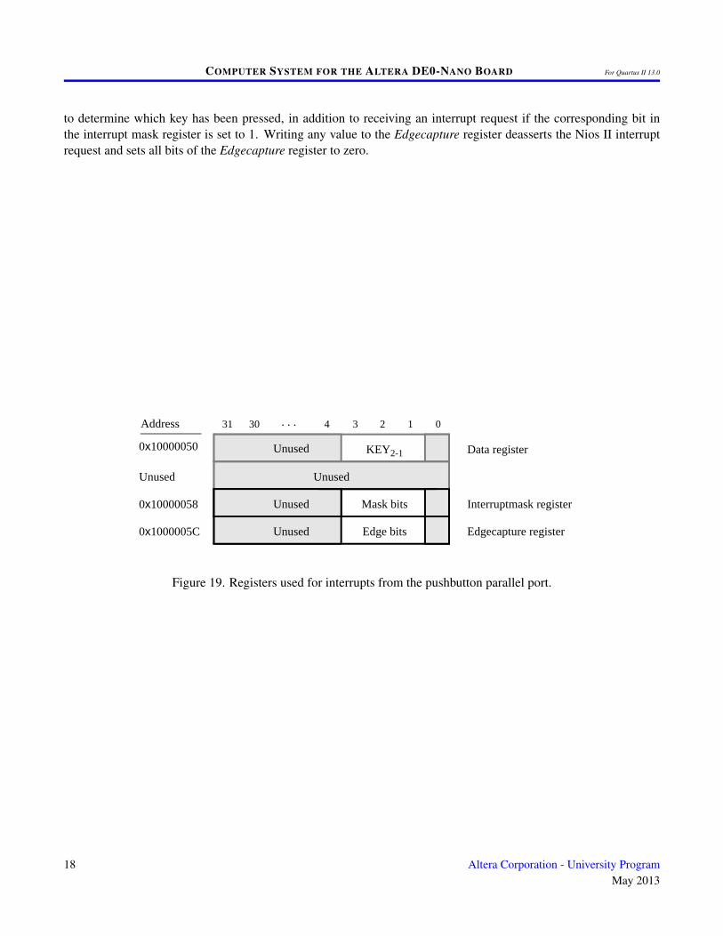
3.1.1 Interrupts from the Pushbutton Switches
Figure 5, reproduced as Figure 19, shows the registers associated with the pushbutton parallel port. The Interrupt-mask register allows processor interrupts to be generated when a key is pressed. Each bit in the Edgecapture registeris set to 1 by the parallel port when the corresponding key is pressed. The Nios II processor can read this register
Altera Corporation - University ProgramMay 2013
17
COMPUTER SYSTEM FOR THE ALTERA DE0-NANO BOARD For Quartus II 13.0
to determine which key has been pressed, in addition to receiving an interrupt request if the corresponding bit inthe interrupt mask register is set to 1. Writing any value to the Edgecapture register deasserts the Nios II interruptrequest and sets all bits of the Edgecapture register to zero.
Address 02 14 331 30 . . .
0x10000050
0x10000058
0x1000005C
Unused
KEY2-1Unused Data register
Interruptmask register
Edgecapture register
Unused
Edge bits
Mask bitsUnused
Unused
Figure 19. Registers used for interrupts from the pushbutton parallel port.
18 Altera Corporation - University ProgramMay 2013
COMPUTER SYSTEM FOR THE ALTERA DE0-NANO BOARD For Quartus II 13.0
3.2 Interrupts from the JTAG UART
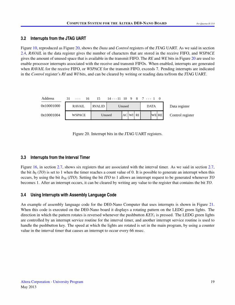
Figure 10, reproduced as Figure 20, shows the Data and Control registers of the JTAG UART. As we said in section2.4, RAVAIL in the data register gives the number of characters that are stored in the receive FIFO, and WSPACEgives the amount of unused space that is available in the transmit FIFO. The RE and WE bits in Figure 20 are used toenable processor interrupts associated with the receive and transmit FIFOs. When enabled, interrupts are generatedwhen RAVAIL for the receive FIFO, or WSPACE for the transmit FIFO, exceeds 7. Pending interrupts are indicatedin the Control register’s RI and WI bits, and can be cleared by writing or reading data to/from the JTAG UART.
Address 0731 16. . .
0x10001000
0x10001004
DATARAVAIL
14 8. . . . . .
WSPACE Unused WI RI WE RE
1
RVALID
AC
10 911
Unused
15
Data register
Control register
Figure 20. Interrupt bits in the JTAG UART registers.
3.3 Interrupts from the Interval Timer
Figure 16, in section 2.7, shows six registers that are associated with the interval timer. As we said in section 2.7,the bit b0 (TO) is set to 1 when the timer reaches a count value of 0. It is possible to generate an interrupt when thisoccurs, by using the bit b16 (ITO). Setting the bit ITO to 1 allows an interrupt request to be generated whenever TObecomes 1. After an interrupt occurs, it can be cleared by writing any value to the register that contains the bit TO.
3.4 Using Interrupts with Assembly Language Code
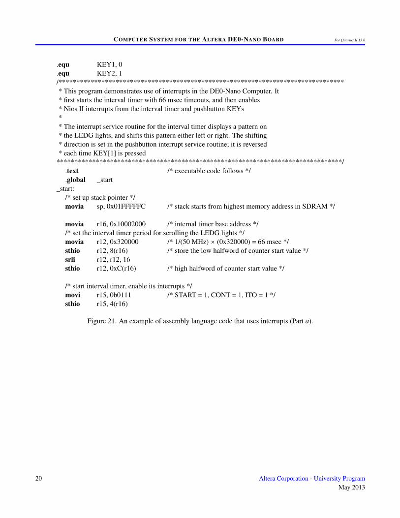
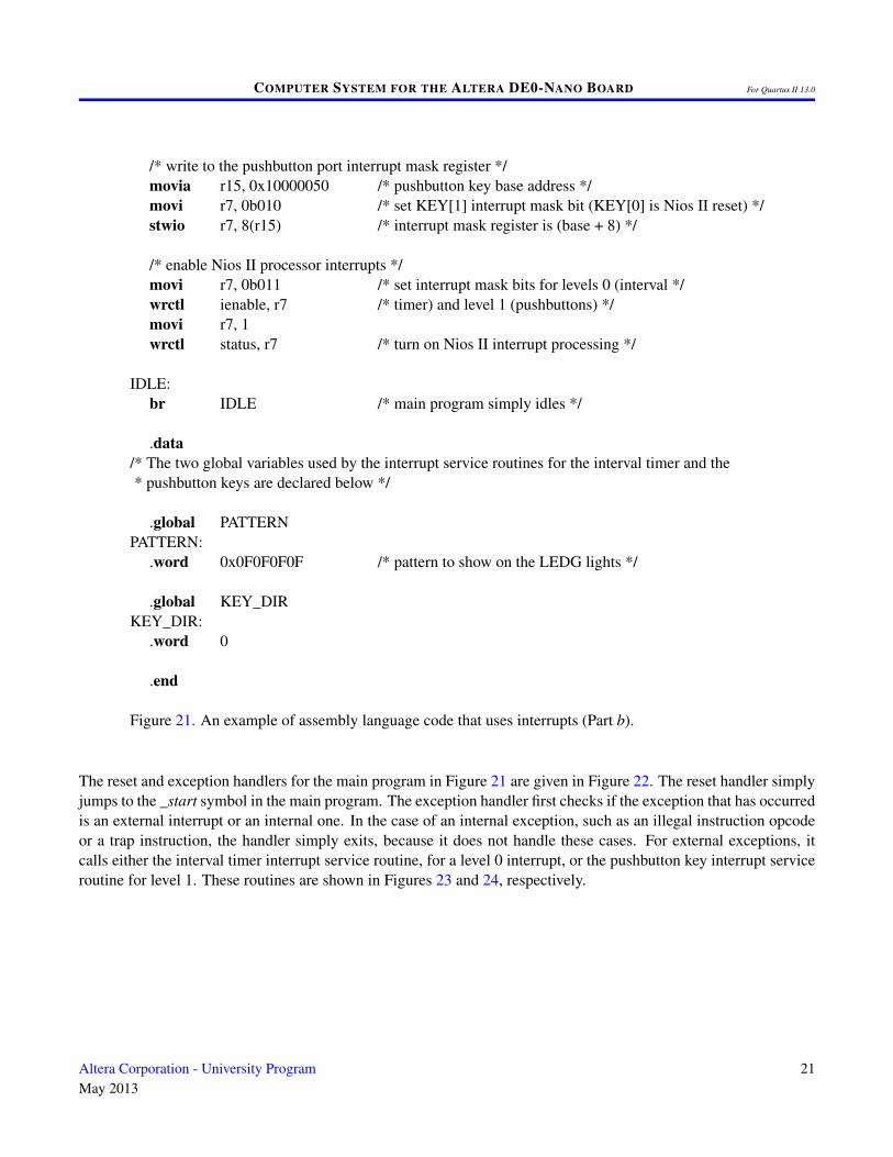
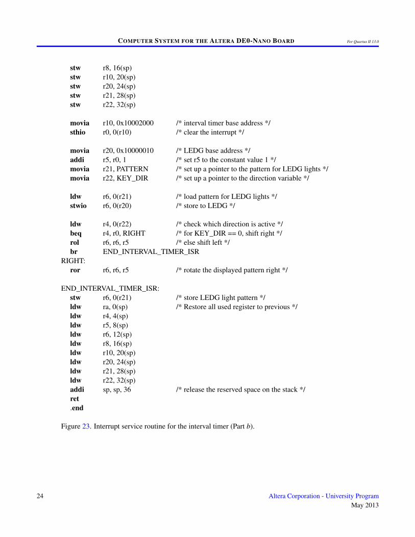
An example of assembly language code for the DE0-Nano Computer that uses interrupts is shown in Figure 21.When this code is executed on the DE0-Nano board it displays a rotating pattern on the LEDG green lights. Thedirection in which the pattern rotates is reversed whenever the pushbutton KEY1 is pressed. The LEDG green lightsare controlled by an interrupt service routine for the interval timer, and another interrupt service routine is used tohandle the pushbutton key. The speed at which the lights are rotated is set in the main program, by using a countervalue in the interval timer that causes an interrupt to occur every 66 msec.
Altera Corporation - University ProgramMay 2013
19
COMPUTER SYSTEM FOR THE ALTERA DE0-NANO BOARD For Quartus II 13.0
.equ KEY1, 0
.equ KEY2, 1/********************************************************************************* This program demonstrates use of interrupts in the DE0-Nano Computer. It* first starts the interval timer with 66 msec timeouts, and then enables* Nios II interrupts from the interval timer and pushbutton KEYs** The interrupt service routine for the interval timer displays a pattern on* the LEDG lights, and shifts this pattern either left or right. The shifting* direction is set in the pushbutton interrupt service routine; it is reversed* each time KEY[1] is pressed
********************************************************************************/.text /* executable code follows */.global _start
_start:/* set up stack pointer */movia sp, 0x01FFFFFC /* stack starts from highest memory address in SDRAM */
movia r16, 0x10002000 /* internal timer base address *//* set the interval timer period for scrolling the LEDG lights */movia r12, 0x320000 /* 1/(50 MHz) × (0x320000) = 66 msec */sthio r12, 8(r16) /* store the low halfword of counter start value */srli r12, r12, 16sthio r12, 0xC(r16) /* high halfword of counter start value */
/* start interval timer, enable its interrupts */movi r15, 0b0111 /* START = 1, CONT = 1, ITO = 1 */sthio r15, 4(r16)
Figure 21. An example of assembly language code that uses interrupts (Part a).
20 Altera Corporation - University ProgramMay 2013
COMPUTER SYSTEM FOR THE ALTERA DE0-NANO BOARD For Quartus II 13.0
/* write to the pushbutton port interrupt mask register */movia r15, 0x10000050 /* pushbutton key base address */movi r7, 0b010 /* set KEY[1] interrupt mask bit (KEY[0] is Nios II reset) */stwio r7, 8(r15) /* interrupt mask register is (base + 8) */
/* enable Nios II processor interrupts */movi r7, 0b011 /* set interrupt mask bits for levels 0 (interval */wrctl ienable, r7 /* timer) and level 1 (pushbuttons) */movi r7, 1wrctl status, r7 /* turn on Nios II interrupt processing */
IDLE:br IDLE /* main program simply idles */
.data/* The two global variables used by the interrupt service routines for the interval timer and the* pushbutton keys are declared below */
.global PATTERNPATTERN:
.word 0x0F0F0F0F /* pattern to show on the LEDG lights */
.global KEY_DIRKEY_DIR:
.word 0
.end
Figure 21. An example of assembly language code that uses interrupts (Part b).
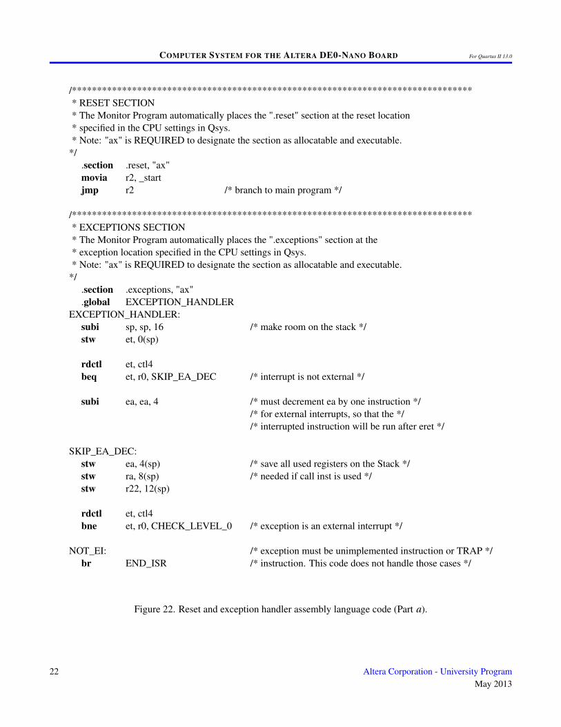
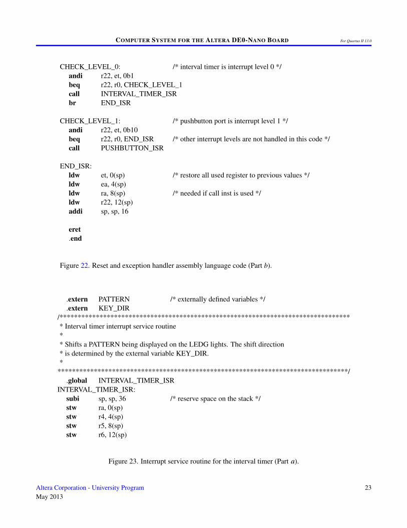
The reset and exception handlers for the main program in Figure 21 are given in Figure 22. The reset handler simplyjumps to the _start symbol in the main program. The exception handler first checks if the exception that has occurredis an external interrupt or an internal one. In the case of an internal exception, such as an illegal instruction opcodeor a trap instruction, the handler simply exits, because it does not handle these cases. For external exceptions, itcalls either the interval timer interrupt service routine, for a level 0 interrupt, or the pushbutton key interrupt serviceroutine for level 1. These routines are shown in Figures 23 and 24, respectively.
Altera Corporation - University ProgramMay 2013
21
COMPUTER SYSTEM FOR THE ALTERA DE0-NANO BOARD For Quartus II 13.0
/********************************************************************************* RESET SECTION* The Monitor Program automatically places the ".reset" section at the reset location* specified in the CPU settings in Qsys.* Note: "ax" is REQUIRED to designate the section as allocatable and executable.
*/.section .reset, "ax"movia r2, _startjmp r2 /* branch to main program */
/********************************************************************************* EXCEPTIONS SECTION* The Monitor Program automatically places the ".exceptions" section at the* exception location specified in the CPU settings in Qsys.* Note: "ax" is REQUIRED to designate the section as allocatable and executable.
*/.section .exceptions, "ax".global EXCEPTION_HANDLER
EXCEPTION_HANDLER:subi sp, sp, 16 /* make room on the stack */stw et, 0(sp)
rdctl et, ctl4beq et, r0, SKIP_EA_DEC /* interrupt is not external */
subi ea, ea, 4 /* must decrement ea by one instruction *//* for external interrupts, so that the *//* interrupted instruction will be run after eret */
SKIP_EA_DEC:stw ea, 4(sp) /* save all used registers on the Stack */stw ra, 8(sp) /* needed if call inst is used */stw r22, 12(sp)
rdctl et, ctl4bne et, r0, CHECK_LEVEL_0 /* exception is an external interrupt */
NOT_EI: /* exception must be unimplemented instruction or TRAP */br END_ISR /* instruction. This code does not handle those cases */
Figure 22. Reset and exception handler assembly language code (Part a).
22 Altera Corporation - University ProgramMay 2013
COMPUTER SYSTEM FOR THE ALTERA DE0-NANO BOARD For Quartus II 13.0
CHECK_LEVEL_0: /* interval timer is interrupt level 0 */andi r22, et, 0b1beq r22, r0, CHECK_LEVEL_1call INTERVAL_TIMER_ISRbr END_ISR
CHECK_LEVEL_1: /* pushbutton port is interrupt level 1 */andi r22, et, 0b10beq r22, r0, END_ISR /* other interrupt levels are not handled in this code */call PUSHBUTTON_ISR
END_ISR:ldw et, 0(sp) /* restore all used register to previous values */ldw ea, 4(sp)ldw ra, 8(sp) /* needed if call inst is used */ldw r22, 12(sp)addi sp, sp, 16
eret.end
Figure 22. Reset and exception handler assembly language code (Part b).
.extern PATTERN /* externally defined variables */
.extern KEY_DIR/********************************************************************************* Interval timer interrupt service routine** Shifts a PATTERN being displayed on the LEDG lights. The shift direction* is determined by the external variable KEY_DIR.*
********************************************************************************/.global INTERVAL_TIMER_ISR
INTERVAL_TIMER_ISR:subi sp, sp, 36 /* reserve space on the stack */stw ra, 0(sp)stw r4, 4(sp)stw r5, 8(sp)stw r6, 12(sp)
Figure 23. Interrupt service routine for the interval timer (Part a).
Altera Corporation - University ProgramMay 2013
23
COMPUTER SYSTEM FOR THE ALTERA DE0-NANO BOARD For Quartus II 13.0
stw r8, 16(sp)stw r10, 20(sp)stw r20, 24(sp)stw r21, 28(sp)stw r22, 32(sp)
movia r10, 0x10002000 /* interval timer base address */sthio r0, 0(r10) /* clear the interrupt */
movia r20, 0x10000010 /* LEDG base address */addi r5, r0, 1 /* set r5 to the constant value 1 */movia r21, PATTERN /* set up a pointer to the pattern for LEDG lights */movia r22, KEY_DIR /* set up a pointer to the direction variable */
ldw r6, 0(r21) /* load pattern for LEDG lights */stwio r6, 0(r20) /* store to LEDG */
ldw r4, 0(r22) /* check which direction is active */beq r4, r0, RIGHT /* for KEY_DIR == 0, shift right */rol r6, r6, r5 /* else shift left */br END_INTERVAL_TIMER_ISR
RIGHT:ror r6, r6, r5 /* rotate the displayed pattern right */
END_INTERVAL_TIMER_ISR:stw r6, 0(r21) /* store LEDG light pattern */ldw ra, 0(sp) /* Restore all used register to previous */ldw r4, 4(sp)ldw r5, 8(sp)ldw r6, 12(sp)ldw r8, 16(sp)ldw r10, 20(sp)ldw r20, 24(sp)ldw r21, 28(sp)ldw r22, 32(sp)addi sp, sp, 36 /* release the reserved space on the stack */ret.end
Figure 23. Interrupt service routine for the interval timer (Part b).
24 Altera Corporation - University ProgramMay 2013
COMPUTER SYSTEM FOR THE ALTERA DE0-NANO BOARD For Quartus II 13.0
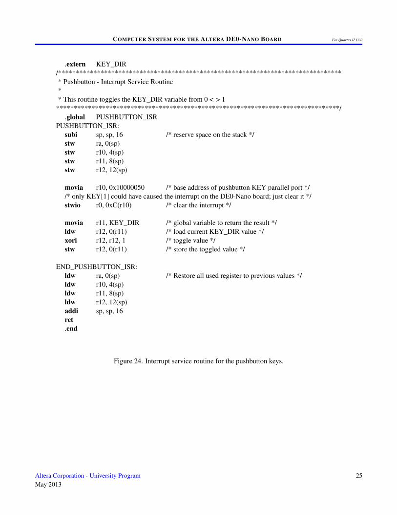
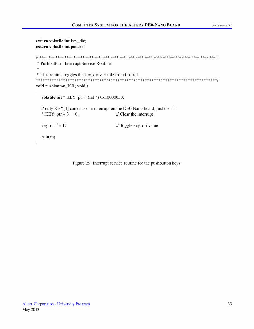
.extern KEY_DIR/********************************************************************************* Pushbutton - Interrupt Service Routine** This routine toggles the KEY_DIR variable from 0 <-> 1
********************************************************************************/.global PUSHBUTTON_ISR
PUSHBUTTON_ISR:subi sp, sp, 16 /* reserve space on the stack */stw ra, 0(sp)stw r10, 4(sp)stw r11, 8(sp)stw r12, 12(sp)
movia r10, 0x10000050 /* base address of pushbutton KEY parallel port *//* only KEY[1] could have caused the interrupt on the DE0-Nano board; just clear it */stwio r0, 0xC(r10) /* clear the interrupt */
movia r11, KEY_DIR /* global variable to return the result */ldw r12, 0(r11) /* load current KEY_DIR value */xori r12, r12, 1 /* toggle value */stw r12, 0(r11) /* store the toggled value */
END_PUSHBUTTON_ISR:ldw ra, 0(sp) /* Restore all used register to previous values */ldw r10, 4(sp)ldw r11, 8(sp)ldw r12, 12(sp)addi sp, sp, 16ret.end
Figure 24. Interrupt service routine for the pushbutton keys.
Altera Corporation - University ProgramMay 2013
25
COMPUTER SYSTEM FOR THE ALTERA DE0-NANO BOARD For Quartus II 13.0
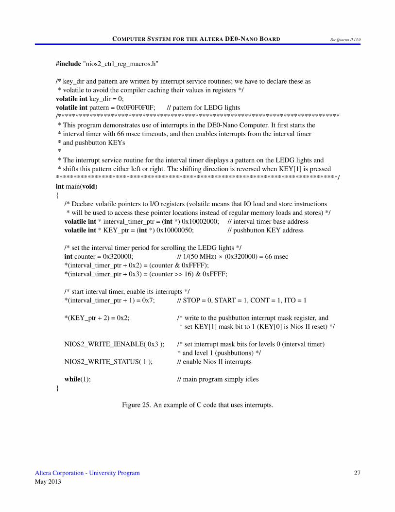
3.5 Using Interrupts with C Language Code
An example of C language code for the DE0-Nano Computer that uses interrupts is shown in Figure 25. This codeperforms exactly the same operations as the code described in Figure 21.
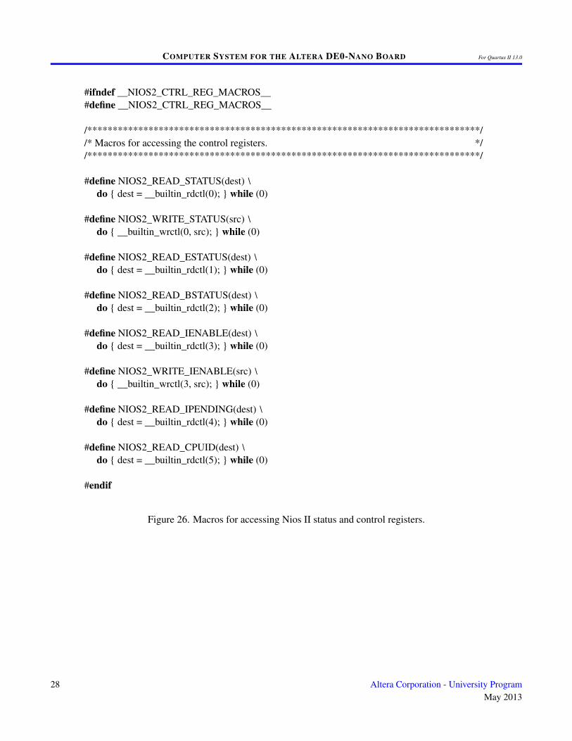
To enable interrupts the code in Figure 25 uses macros that provide access to the Nios II status and control registers.A collection of such macros, which can be used in any C program, are provided in Figure 26.
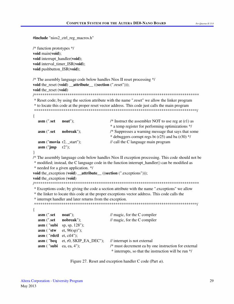
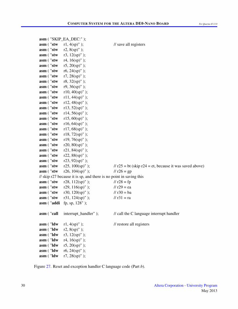
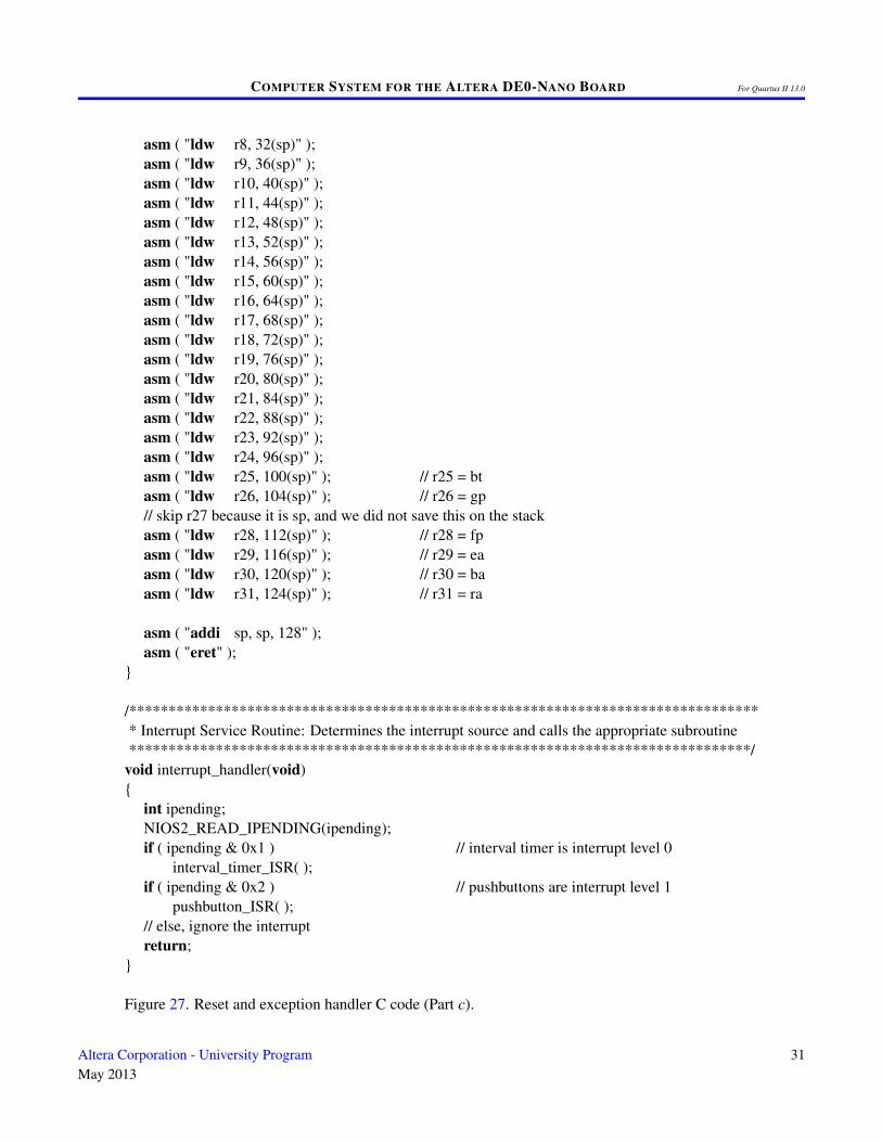
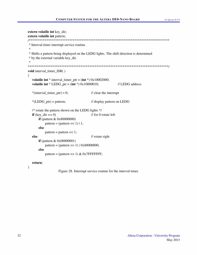
The reset and exception handlers for the main program in Figure 25 are given in Figure 27. The function calledthe_reset provides a simple reset mechanism by performing a branch to the main program. The function namedthe_exception represents a general exception handler that can be used with any C program. It includes assemblylanguage code to check if the exception is caused by an external interrupt, and, if so, calls a C language routinenamed interrupt_handler. This routine can then perform whatever action is needed for the specific application.In Figure 27, the interrupt_handler code first determines which exception has occurred, by using a macro fromFigure 26 that reads the content of the Nios II interrupt pending register. The interrupt service routine that isinvoked for the interval timer is shown in 28, and the interrupt service routine for the pushbutton switches appearsin Figure 29.
The source code files shown in Figure 21 to Figure 29 are distributed as part of the Altera Monitor Program. Thefiles can be found under the heading sample programs, and are identified by the name Interrupt Example.
26 Altera Corporation - University ProgramMay 2013
COMPUTER SYSTEM FOR THE ALTERA DE0-NANO BOARD For Quartus II 13.0
#include "nios2_ctrl_reg_macros.h"
/* key_dir and pattern are written by interrupt service routines; we have to declare these as* volatile to avoid the compiler caching their values in registers */
volatile int key_dir = 0;volatile int pattern = 0x0F0F0F0F; // pattern for LEDG lights/********************************************************************************* This program demonstrates use of interrupts in the DE0-Nano Computer. It first starts the* interval timer with 66 msec timeouts, and then enables interrupts from the interval timer* and pushbutton KEYs** The interrupt service routine for the interval timer displays a pattern on the LEDG lights and* shifts this pattern either left or right. The shifting direction is reversed when KEY[1] is pressed
********************************************************************************/int main(void){
/* Declare volatile pointers to I/O registers (volatile means that IO load and store instructions* will be used to access these pointer locations instead of regular memory loads and stores) */
volatile int * interval_timer_ptr = (int *) 0x10002000; // interval timer base addressvolatile int * KEY_ptr = (int *) 0x10000050; // pushbutton KEY address
/* set the interval timer period for scrolling the LEDG lights */int counter = 0x320000; // 1/(50 MHz) × (0x320000) = 66 msec*(interval_timer_ptr + 0x2) = (counter & 0xFFFF);*(interval_timer_ptr + 0x3) = (counter >> 16) & 0xFFFF;
/* start interval timer, enable its interrupts */*(interval_timer_ptr + 1) = 0x7; // STOP = 0, START = 1, CONT = 1, ITO = 1
*(KEY_ptr + 2) = 0x2; /* write to the pushbutton interrupt mask register, and* set KEY[1] mask bit to 1 (KEY[0] is Nios II reset) */
NIOS2_WRITE_IENABLE( 0x3 ); /* set interrupt mask bits for levels 0 (interval timer)* and level 1 (pushbuttons) */
NIOS2_WRITE_STATUS( 1 ); // enable Nios II interrupts
while(1); // main program simply idles}
Figure 25. An example of C code that uses interrupts.
Altera Corporation - University ProgramMay 2013
27
COMPUTER SYSTEM FOR THE ALTERA DE0-NANO BOARD For Quartus II 13.0
#ifndef __NIOS2_CTRL_REG_MACROS__#define __NIOS2_CTRL_REG_MACROS__
/*****************************************************************************//* Macros for accessing the control registers. *//*****************************************************************************/
#define NIOS2_READ_STATUS(dest) \do { dest = __builtin_rdctl(0); } while (0)
#define NIOS2_WRITE_STATUS(src) \do { __builtin_wrctl(0, src); } while (0)
#define NIOS2_READ_ESTATUS(dest) \do { dest = __builtin_rdctl(1); } while (0)
#define NIOS2_READ_BSTATUS(dest) \do { dest = __builtin_rdctl(2); } while (0)
#define NIOS2_READ_IENABLE(dest) \do { dest = __builtin_rdctl(3); } while (0)
#define NIOS2_WRITE_IENABLE(src) \do { __builtin_wrctl(3, src); } while (0)
#define NIOS2_READ_IPENDING(dest) \do { dest = __builtin_rdctl(4); } while (0)
#define NIOS2_READ_CPUID(dest) \do { dest = __builtin_rdctl(5); } while (0)
#endif
Figure 26. Macros for accessing Nios II status and control registers.
28 Altera Corporation - University ProgramMay 2013
COMPUTER SYSTEM FOR THE ALTERA DE0-NANO BOARD For Quartus II 13.0
#include "nios2_ctrl_reg_macros.h"
/* function prototypes */void main(void);void interrupt_handler(void);void interval_timer_ISR(void);void pushbutton_ISR(void);
/* The assembly language code below handles Nios II reset processing */void the_reset (void) __attribute__ ((section (".reset")));void the_reset (void)/******************************************************************************** Reset code; by using the section attribute with the name ".reset" we allow the linker program* to locate this code at the proper reset vector address. This code just calls the main program******************************************************************************/
{asm (".set noat"); /* Instruct the assembler NOT to use reg at (r1) as
* a temp register for performing optimizations */asm (".set nobreak"); /* Suppresses a warning message that says that some
* debuggers corrupt regs bt (r25) and ba (r30) */asm ("movia r2, _start"); // call the C language main programasm ("jmp r2");
}/* The assembly language code below handles Nios II exception processing. This code should not be* modified; instead, the C language code in the function interrupt_handler() can be modified as* needed for a given application. */
void the_exception (void) __attribute__ ((section (".exceptions")));void the_exception (void)/******************************************************************************** Exceptions code; by giving the code a section attribute with the name ".exceptions" we allow* the linker to locate this code at the proper exceptions vector address. This code calls the* interrupt handler and later returns from the exception.******************************************************************************/
{asm (".set noat"); // magic, for the C compilerasm (".set nobreak"); // magic, for the C compilerasm ( "subi sp, sp, 128");asm ( "stw et, 96(sp)");asm ( "rdctl et, ctl4");asm ( "beq et, r0, SKIP_EA_DEC"); // interrupt is not externalasm ( "subi ea, ea, 4"); /* must decrement ea by one instruction for external
* interrupts, so that the instruction will be run */
Figure 27. Reset and exception handler C code (Part a).
Altera Corporation - University ProgramMay 2013
29
COMPUTER SYSTEM FOR THE ALTERA DE0-NANO BOARD For Quartus II 13.0
asm ( "SKIP_EA_DEC:" );asm ( "stw r1, 4(sp)" ); // save all registersasm ( "stw r2, 8(sp)" );asm ( "stw r3, 12(sp)" );asm ( "stw r4, 16(sp)" );asm ( "stw r5, 20(sp)" );asm ( "stw r6, 24(sp)" );asm ( "stw r7, 28(sp)" );asm ( "stw r8, 32(sp)" );asm ( "stw r9, 36(sp)" );asm ( "stw r10, 40(sp)" );asm ( "stw r11, 44(sp)" );asm ( "stw r12, 48(sp)" );asm ( "stw r13, 52(sp)" );asm ( "stw r14, 56(sp)" );asm ( "stw r15, 60(sp)" );asm ( "stw r16, 64(sp)" );asm ( "stw r17, 68(sp)" );asm ( "stw r18, 72(sp)" );asm ( "stw r19, 76(sp)" );asm ( "stw r20, 80(sp)" );asm ( "stw r21, 84(sp)" );asm ( "stw r22, 88(sp)" );asm ( "stw r23, 92(sp)" );asm ( "stw r25, 100(sp)" ); // r25 = bt (skip r24 = et, because it was saved above)asm ( "stw r26, 104(sp)" ); // r26 = gp// skip r27 because it is sp, and there is no point in saving thisasm ( "stw r28, 112(sp)" ); // r28 = fpasm ( "stw r29, 116(sp)" ); // r29 = eaasm ( "stw r30, 120(sp)" ); // r30 = baasm ( "stw r31, 124(sp)" ); // r31 = raasm ( "addi fp, sp, 128" );
asm ( "call interrupt_handler" ); // call the C language interrupt handler
asm ( "ldw r1, 4(sp)" ); // restore all registersasm ( "ldw r2, 8(sp)" );asm ( "ldw r3, 12(sp)" );asm ( "ldw r4, 16(sp)" );asm ( "ldw r5, 20(sp)" );asm ( "ldw r6, 24(sp)" );asm ( "ldw r7, 28(sp)" );
Figure 27. Reset and exception handler C language code (Part b).
30 Altera Corporation - University ProgramMay 2013
COMPUTER SYSTEM FOR THE ALTERA DE0-NANO BOARD For Quartus II 13.0
asm ( "ldw r8, 32(sp)" );asm ( "ldw r9, 36(sp)" );asm ( "ldw r10, 40(sp)" );asm ( "ldw r11, 44(sp)" );asm ( "ldw r12, 48(sp)" );asm ( "ldw r13, 52(sp)" );asm ( "ldw r14, 56(sp)" );asm ( "ldw r15, 60(sp)" );asm ( "ldw r16, 64(sp)" );asm ( "ldw r17, 68(sp)" );asm ( "ldw r18, 72(sp)" );asm ( "ldw r19, 76(sp)" );asm ( "ldw r20, 80(sp)" );asm ( "ldw r21, 84(sp)" );asm ( "ldw r22, 88(sp)" );asm ( "ldw r23, 92(sp)" );asm ( "ldw r24, 96(sp)" );asm ( "ldw r25, 100(sp)" ); // r25 = btasm ( "ldw r26, 104(sp)" ); // r26 = gp// skip r27 because it is sp, and we did not save this on the stackasm ( "ldw r28, 112(sp)" ); // r28 = fpasm ( "ldw r29, 116(sp)" ); // r29 = eaasm ( "ldw r30, 120(sp)" ); // r30 = baasm ( "ldw r31, 124(sp)" ); // r31 = ra
asm ( "addi sp, sp, 128" );asm ( "eret" );
}
/********************************************************************************* Interrupt Service Routine: Determines the interrupt source and calls the appropriate subroutine*******************************************************************************/
void interrupt_handler(void){
int ipending;NIOS2_READ_IPENDING(ipending);if ( ipending & 0x1 ) // interval timer is interrupt level 0
interval_timer_ISR( );if ( ipending & 0x2 ) // pushbuttons are interrupt level 1
pushbutton_ISR( );// else, ignore the interruptreturn;
}
Figure 27. Reset and exception handler C code (Part c).
Altera Corporation - University ProgramMay 2013
31
COMPUTER SYSTEM FOR THE ALTERA DE0-NANO BOARD For Quartus II 13.0
extern volatile int key_dir;extern volatile int pattern;/********************************************************************************* Interval timer interrupt service routine** Shifts a pattern being displayed on the LEDG lights. The shift direction is determined* by the external variable key_dir.*
********************************************************************************/void interval_timer_ISR( ){
volatile int * interval_timer_ptr = (int *) 0x10002000;volatile int * LEDG_ptr = (int *) 0x10000010; // LEDG address
*(interval_timer_ptr) = 0; // clear the interrupt
*(LEDG_ptr) = pattern; // display pattern on LEDG
/* rotate the pattern shown on the LEDG lights */if (key_dir == 0) // for 0 rotate left
if (pattern & 0x80000000)pattern = (pattern << 1) | 1;
elsepattern = pattern << 1;
else // rotate rightif (pattern & 0x00000001)
pattern = (pattern >> 1) | 0x80000000;else
pattern = (pattern >> 1) & 0x7FFFFFFF;
return;}
Figure 28. Interrupt service routine for the interval timer.
32 Altera Corporation - University ProgramMay 2013
COMPUTER SYSTEM FOR THE ALTERA DE0-NANO BOARD For Quartus II 13.0
extern volatile int key_dir;extern volatile int pattern;
/********************************************************************************* Pushbutton - Interrupt Service Routine** This routine toggles the key_dir variable from 0 <-> 1
********************************************************************************/void pushbutton_ISR( void ){
volatile int * KEY_ptr = (int *) 0x10000050;
// only KEY[1] can cause an interrupt on the DE0-Nano board; just clear it*(KEY_ptr + 3) = 0; // Clear the interrupt
key_dir ∧= 1; // Toggle key_dir value
return;}
Figure 29. Interrupt service routine for the pushbutton keys.
Altera Corporation - University ProgramMay 2013
33
COMPUTER SYSTEM FOR THE ALTERA DE0-NANO BOARD For Quartus II 13.0
4 Modifying the DE0-Nano Computer
It is possible to modify the DE0-Nano Computer by using Altera’s Quartus II software and Qsys System Integrationtool. Tutorials that introduce this software are provided in the University Program section of Altera’s web site. Tomodify the system it is first necessary to obtain all of the relevant design source code files. The DE0-Nano Computeris available in two versions that specify the system using either Verilog HDL or VHDL. After these files have beenobtained it is also necessary to install the source code for the I/O peripherals in the system. These peripherals areprovided in the form of Qsys IP cores and are included in a package available from Altera’s University Program website, called the Altera University Program IP Cores
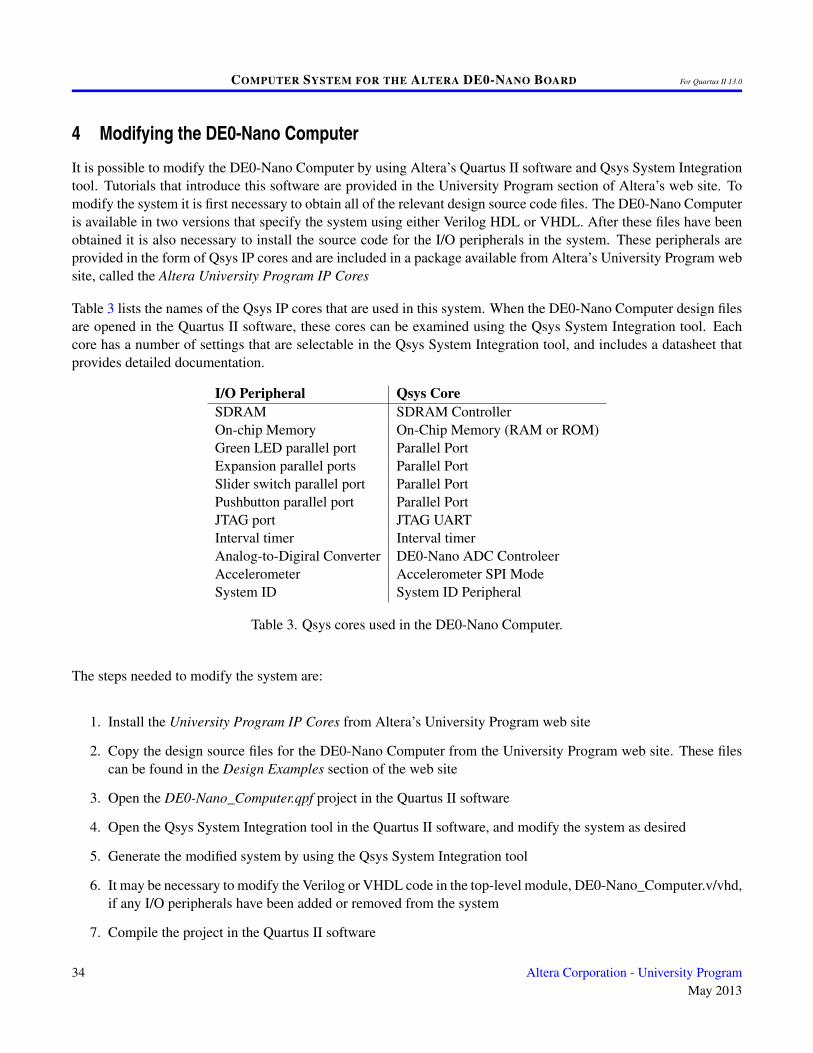
Table 3 lists the names of the Qsys IP cores that are used in this system. When the DE0-Nano Computer design filesare opened in the Quartus II software, these cores can be examined using the Qsys System Integration tool. Eachcore has a number of settings that are selectable in the Qsys System Integration tool, and includes a datasheet thatprovides detailed documentation.
I/O Peripheral Qsys CoreSDRAM SDRAM ControllerOn-chip Memory On-Chip Memory (RAM or ROM)Green LED parallel port Parallel PortExpansion parallel ports Parallel PortSlider switch parallel port Parallel PortPushbutton parallel port Parallel PortJTAG port JTAG UARTInterval timer Interval timerAnalog-to-Digiral Converter DE0-Nano ADC ControleerAccelerometer Accelerometer SPI ModeSystem ID System ID Peripheral
Table 3. Qsys cores used in the DE0-Nano Computer.
The steps needed to modify the system are:
1. Install the University Program IP Cores from Altera’s University Program web site
2. Copy the design source files for the DE0-Nano Computer from the University Program web site. These filescan be found in the Design Examples section of the web site
3. Open the DE0-Nano_Computer.qpf project in the Quartus II software
4. Open the Qsys System Integration tool in the Quartus II software, and modify the system as desired
5. Generate the modified system by using the Qsys System Integration tool
6. It may be necessary to modify the Verilog or VHDL code in the top-level module, DE0-Nano_Computer.v/vhd,if any I/O peripherals have been added or removed from the system
7. Compile the project in the Quartus II software
34 Altera Corporation - University ProgramMay 2013
COMPUTER SYSTEM FOR THE ALTERA DE0-NANO BOARD For Quartus II 13.0
8. Download the modified system into the DE0-Nano board
The DE0-Nano Computer includes a Nios II/f processor. When using the Quartus II Web Edition, compiling adesign with a Nios II/s or Nios II/f processor will produce a time-limited SOF file. As a result, the board mustremain connected to the host computer, and the design cannot be set as the default configuration, as discussed inSection 5. Designs using only Nios II/e processors and designs compiled using the Quartus II Subscription Editiondo not have this restriction.
5 Making the System the Default Configuration
The DE0-Nano Computer can be loaded into the nonvolatile FPGA configuration memory on the DE0-Nano board,so that it becomes the default system whenever the board is powered on. Instructions for configuring the DE0-Nanoboard in this manner can be found in the tutorial Introduction to the Quartus II Software, which is available fromAltera’s University Program.
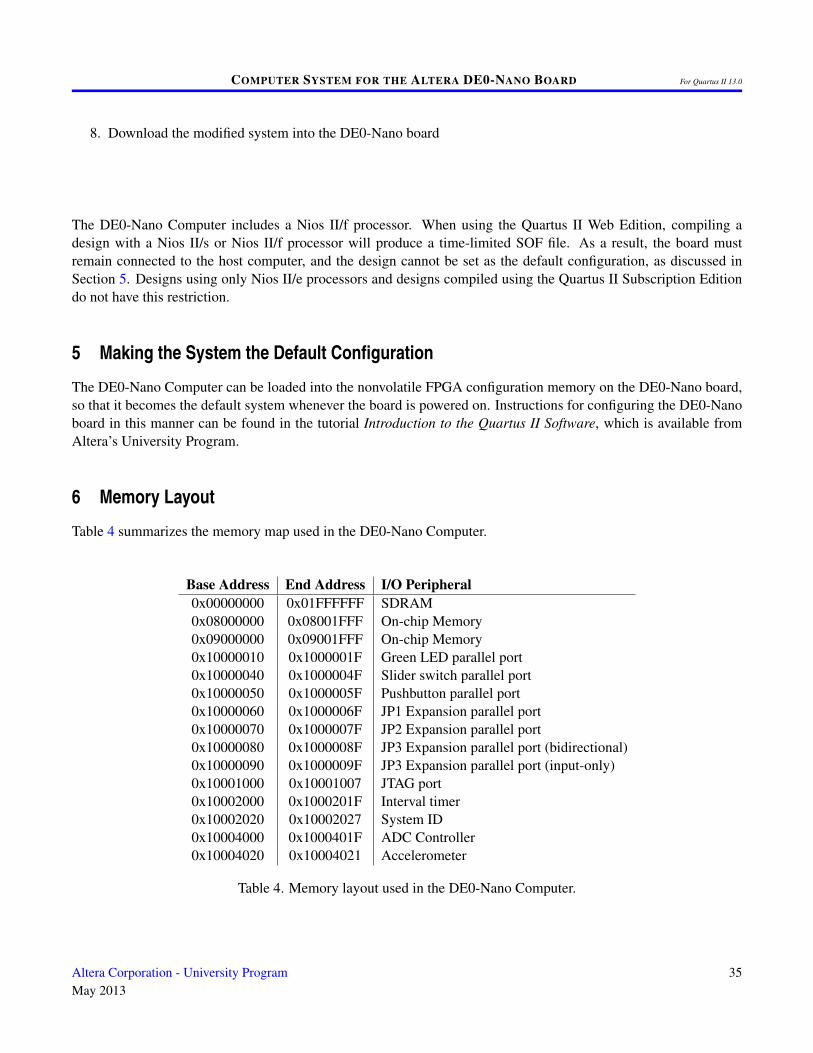
6 Memory Layout
Table 4 summarizes the memory map used in the DE0-Nano Computer.
Base Address End Address I/O Peripheral0x00000000 0x01FFFFFF SDRAM0x08000000 0x08001FFF On-chip Memory0x09000000 0x09001FFF On-chip Memory0x10000010 0x1000001F Green LED parallel port0x10000040 0x1000004F Slider switch parallel port0x10000050 0x1000005F Pushbutton parallel port0x10000060 0x1000006F JP1 Expansion parallel port0x10000070 0x1000007F JP2 Expansion parallel port0x10000080 0x1000008F JP3 Expansion parallel port (bidirectional)0x10000090 0x1000009F JP3 Expansion parallel port (input-only)0x10001000 0x10001007 JTAG port0x10002000 0x1000201F Interval timer0x10002020 0x10002027 System ID0x10004000 0x1000401F ADC Controller0x10004020 0x10004021 Accelerometer
Table 4. Memory layout used in the DE0-Nano Computer.
Altera Corporation - University ProgramMay 2013
35
COMPUTER SYSTEM FOR THE ALTERA DE0-NANO BOARD For Quartus II 13.0
7 Altera Monitor Program Integration
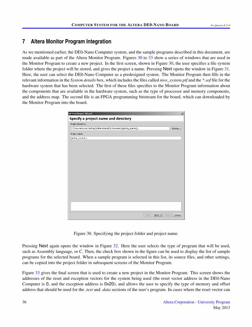
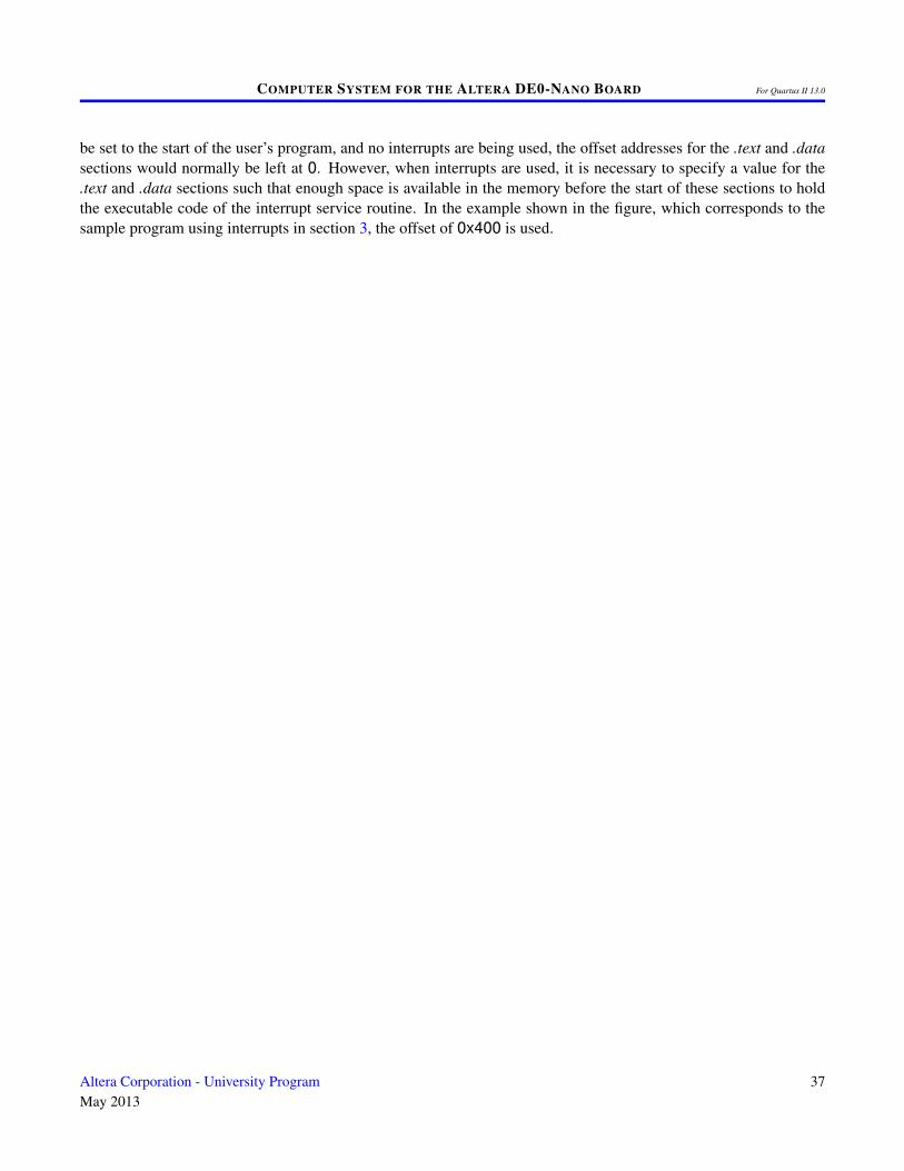
As we mentioned earlier, the DE0-Nano Computer system, and the sample programs described in this document, aremade available as part of the Altera Monitor Program. Figures 30 to 33 show a series of windows that are used inthe Monitor Program to create a new project. In the first screen, shown in Figure 30, the user specifies a file systemfolder where the project will be stored, and gives the project a name. Pressing Next opens the window in Figure 31.Here, the user can select the DE0-Nano Computer as a predesigned system. The Monitor Program then fills in therelevant information in the System details box, which includes the files called nios_system.ptf and the *.sof file for thehardware system that has been selected. The first of these files specifies to the Monitor Program information aboutthe components that are available in the hardware system, such as the type of processor and memory components,and the address map. The second file is an FPGA programming bitstream for the board, which can downloaded bythe Monitor Program into the board.
Figure 30. Specifying the project folder and project name.
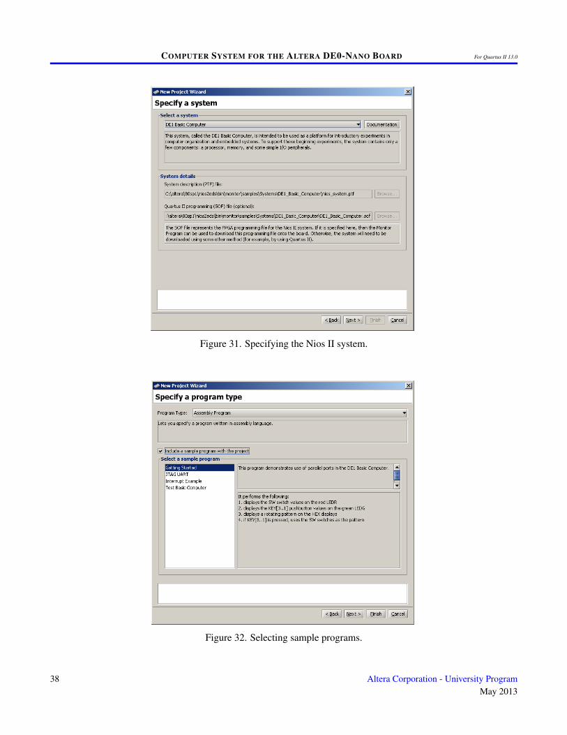
Pressing Next again opens the window in Figure 32. Here the user selects the type of program that will be used,such as Assembly language, or C. Then, the check box shown in the figure can be used to display the list of sampleprograms for the selected board. When a sample program is selected in this list, its source files, and other settings,can be copied into the project folder in subsequent screens of the Monitor Program.
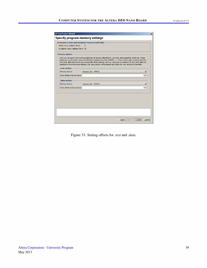
Figure 33 gives the final screen that is used to create a new project in the Monitor Program. This screen shows theaddresses of the reset and exception vectors for the system being used (the reset vector address in the DE0-NanoComputer is 0, and the exception address is 0x20), and allows the user to specify the type of memory and offsetaddress that should be used for the .text and .data sections of the user’s program. In cases where the reset vector can
36 Altera Corporation - University ProgramMay 2013
COMPUTER SYSTEM FOR THE ALTERA DE0-NANO BOARD For Quartus II 13.0
be set to the start of the user’s program, and no interrupts are being used, the offset addresses for the .text and .datasections would normally be left at 0. However, when interrupts are used, it is necessary to specify a value for the.text and .data sections such that enough space is available in the memory before the start of these sections to holdthe executable code of the interrupt service routine. In the example shown in the figure, which corresponds to thesample program using interrupts in section 3, the offset of 0x400 is used.
Altera Corporation - University ProgramMay 2013
37
COMPUTER SYSTEM FOR THE ALTERA DE0-NANO BOARD For Quartus II 13.0
Figure 31. Specifying the Nios II system.
Figure 32. Selecting sample programs.
38 Altera Corporation - University ProgramMay 2013
COMPUTER SYSTEM FOR THE ALTERA DE0-NANO BOARD For Quartus II 13.0
Figure 33. Setting offsets for .text and .data.
Altera Corporation - University ProgramMay 2013
39