DDRn Interface Signoff Analysis with Distributed Chip IO ... · PDF fileDDRn Interface Signoff...
29
Steven Guo Spreadtrum Zuli Qin Zhangmin Zhong Cadence IBIS Asia Summit Shanghai,China Nov. 15, 2013 DDRn Interface Signoff Analysis with Distributed Chip IO Interconnect Model
Transcript of DDRn Interface Signoff Analysis with Distributed Chip IO ... · PDF fileDDRn Interface Signoff...

Steven Guo Spreadtrum
Zuli Qin Zhangmin Zhong Cadence
IBIS Asia Summit
Shanghai,China
Nov. 15, 2013
DDRn Interface Signoff Analysis with Distributed Chip
IO Interconnect Model

Agenda
Introduction About the Chip IO Interconnection
Chip IO Interconnect Model Extraction and Analysis
Case Study – DDR SSO and Chip IO Power Decap
Summary

. 3
Simplified View of a Smartphone Board
4Gb eMMC +8Gb LPDDR2 Memory
eMCP (LPDDR2+eMMC) 11.5x13x1.0mm3 162b FBGA 0.5mm pitch
12x12 PoP + eMMC only 11.5x13x1.0mm3 153b FBGA 0.5mm pitch
eMCP (LPDDR2+ eMMC)
eMCP (LPDDR3+ eMMC)
PoP (LPDDR2) + eMMC
PoP (LPDDR3) + eMMC

Chip IO interconnection Structure

DDRn System Interconnection Topology
eMCP / PoP Memory
LPDDR2/LPDDR3
Chip Model = Distributed IO
Power/Ground/Signal
Interconnect Model (from M1 to
Bump)
S-Parameter or Broadband
Spice model
Chip
Model
CPU DDRn Ctrl
Chip Model

Uncertainties Vs Timing Margin
DQ
DQS
Setup Hold DQ
DQS
Setup
Margin
Hold
Margin
Transmitter Receiver

DDRn Setup/Hold Timing Budgets (Uncertainties : Skew & Jitter)
Transmitter Contributions Interconnection
Contributions Receiver
Contributions
DDL (Data Delay Line) Granularity and bit offset (BDL and LCDL ) (Static)
Signal Length Mismatches (On-chip interconnection M1 to Bump , RDL Routing , Package Substrate and PCB layout Skew) (Static)
Input Rise /Fall Slew Factor (Static)
Register Mismatch within the PHY (Static) Crosstalk (Pushout/Pullin from nearby aggressor signals and serpentine routing ) (Dynamic)
DDRn Data Set Up and Hold specifications (tDS, tDH) (Static)
DLL Jitter including Clock Source Jitter (Dynamic) Reflections,Inter-Symbol Interference (ISI) (Impedance discontinuities, topology,loading) (Dynamic)
Setup and Hold Slew rate Derating (Static)
DLL Phase Error (Dynamic) High frequency losses (Dielectric and Conductor losses) (Dynamic)
PHY Skew between DQS/DQS# and DQ signals (Static) Dielectric mismatches between layers (Dynamic)
Process Variation Effects (Static)
IO Output Rise Fall Delay Mismatch (Static)
SSO/SSN Pushout (Effects of non-ideal power distribution network-PDN) (Dynamic)
VT Drift (BDL and LCDL Setting) (Dynamic)
Agenda
Introduction About the Chip IO Interconnection
Chip IO Interconnect Model Extraction and Analysis
Case Study – DDR SSO and Chip IO Power Decap
Summary

Inputs
• LEF/DEF or GDS
• Technology file (.ict)
• Layer map file
Outputs
• IO interconnect model – SPICE netlist
• EPA results – Power pin RL
– Power net capacitance
– Power net impedance
– Signal net RLC
– Signal net return and insertion loss
Electrical
Performance
Assessment
What-if Analysis Model Generation
Technology file and configuration file GDS GUI
SPICE
Netlist
Chip IO Interconnect Model Extraction Diagram
.ict and
Map File
Chip
GDS
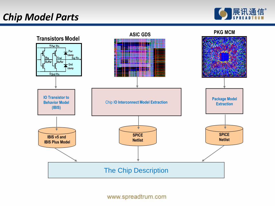
Chip Model Parts
PKG MCM
SPICE
Netlist
The Chip Description
Transistors Model
IO Transistor to
Behavior Model
(IBIS)
IBIS v5 and
IBIS Plus Model
Package Model
Extraction
ASIC GDS
IO
Interconnect
Model
Extraction with
XcitePI
SPICE
Netlist
Chip IO Interconnect Model Extraction
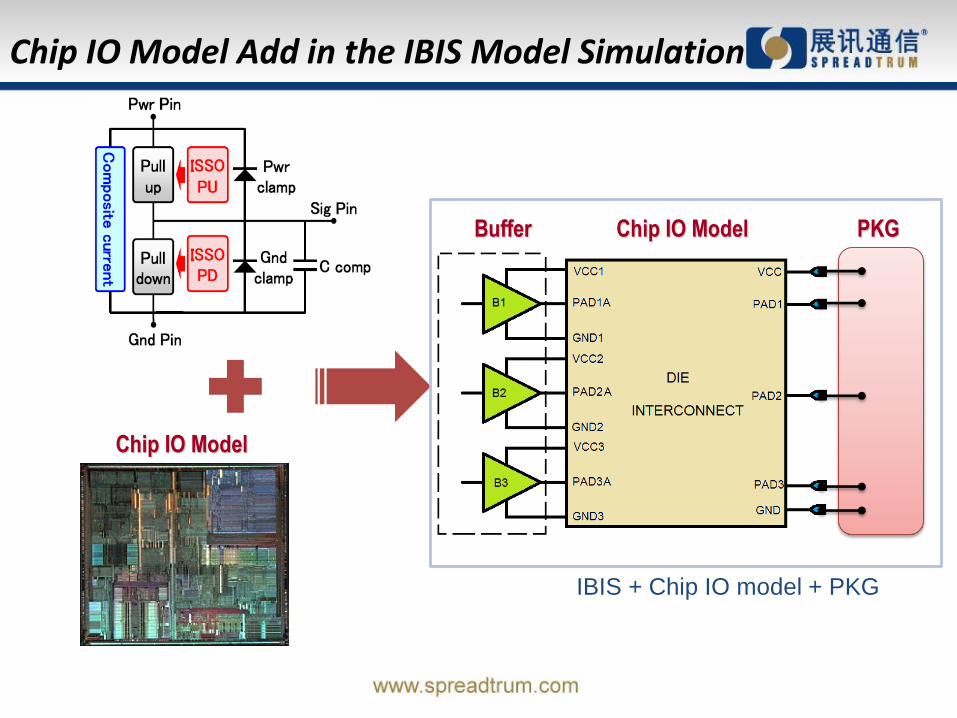
Chip IO Model Add in the IBIS Model Simulation
Chip IO Model
IBIS + Chip IO model + PKG
Chip IO Model Buffer PKG

Input
Buffer RX
Main
Buffer
VDD_IO
Main
Buffer
Receiv
er
VRM
Main
Buffer
Input
Buffer
Driv
er
Package PCB
System Interconnection Analysis for DDRn
• Chip IO interconnect model includes signals and IO pwr/gnd
• Chip IO interconnect model is extracted by chip level extractor which include RLCK elements.
• PCB and package are extracted by EM solver and converted into broadband SPICE model.
Chip
VSS

Agenda
Introduction About the Chip IO Interconnection
Chip IO Interconnect Model Extraction and Analysis
Case Study – DDR SSO and Chip IO Power Decap
Summary

Test vehicle of system level SI/PI analysis (DQ/DQS)
Package merged with PCB
Chip IO interconnection model extraction

DDRn Bank0 SSO

Power aware signal integrity analysis System level SI/PI analysis (DQ/DQS) with memory write in TD—ODT40
Bank0

Power aware signal integrity analysis System level SI/PI analysis (DQ/DQS) with memory write in TD—ODT60
Bank0

Test vehicle of system level SI/PI analysis coupling among ADD/CMD/CLK and DQ/DQS
Package merged with PCB
Build ADD/CMD/CLK and bank0 groups
Chip IO model extraction

Test vehicle of system level SI/PI analysis coupling among ADD/CMD/CLK and DQ/DQS
• Running DQ/DQS patterns first then turn on ADD/CLK.
• To measure ADD/CLK lines noise while DQ/DQS are toggling.
• To monitor ADD/CLK waveform and see if they are affected by DQ/DQS
• All DQ/DQS are in ODT-off
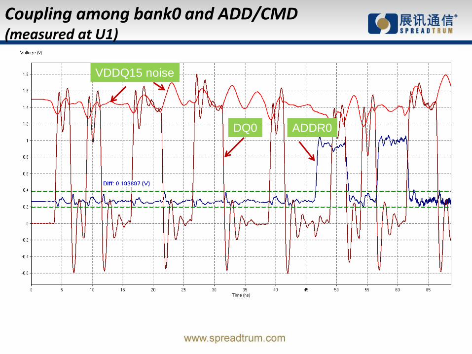
Coupling among bank0 and ADD/CMD (measured at U1)
DQ0
VDDQ15 noise
ADDR0

Coupling among bank0 and ADD/CMD (measured at U3)
DQ0
VDDQ15 noise
ADDR0

• Ports for IO cells which can be impedance observations
• Ports for PSCAP/MOS cap cells which can be decaps and optimized
Port for MOS cap
Ports for I/O cells
Chip Decap What-if Analysis and Optimization

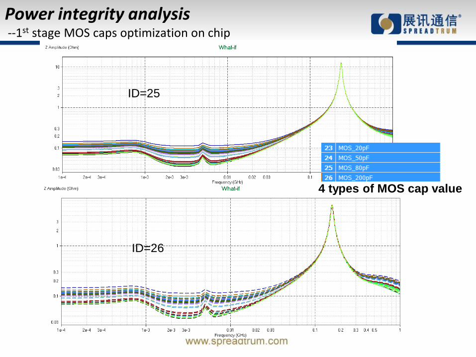
Power integrity analysis
--1st stage MOS caps optimization on chip
ID=23
ID=24
4 types of MOS cap value
Power integrity analysis --1st stage MOS caps optimization on chip
ID=25
ID=26
4 types of MOS cap value
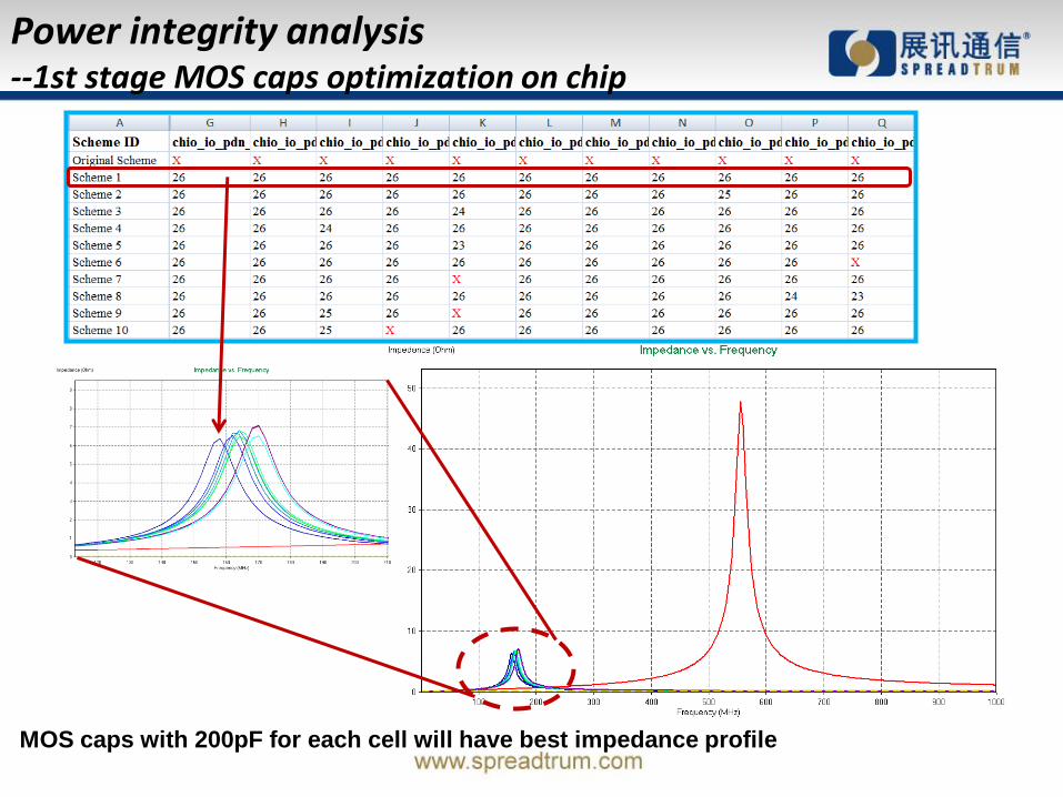
Power integrity analysis --1st stage MOS caps optimization on chip
MOS caps with 200pF for each cell will have best impedance profile

Chip Decap What-if Analysis and Optimization
• This is the definition of big cell with x7 small and x1 large cells
• Total value for this big cell is ranging from 20,50,80,200PF.
• A strongly recommendation that places MOS caps as much as possible
Agenda
Introduction About the Chip IO Interconnection
Chip IO Interconnect Model Extraction and Analysis
Case Study – DDR SSO and Chip IO Power Decap
Summary

Summary
• Chip IO interconnect model should include IO Power/Ground/Signal Interconnect Model
• For high speed and low power DDR systems (LPDDR3/DDR3L/DDR4), Chip IO interconnect model is crucial for IO-SSO analysis.
• Chip IO interconnect model is one part for Chip but not in IBIS model.
• With Chip IO Interconnection model, Chip vendor can do more accurate DDRn signoff analysis to predict System electrical performace before ASIC tapeout.
• On-die RC or better distributed chip IO interconnect model can be more realistic for signal/power analysis
• New System Signoff methodology enable to avoid overdesign or under-design for on-die Decap Cell