datasheet (1)
9
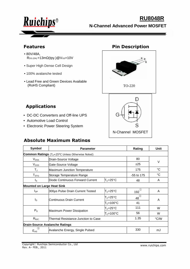
Copyright Ruichips Semiconductor Co., Ltd Rev. A– FEB., 2011 www.ruichips.com RU8048R N-Channel Advanced Power MOSFET Features Pin Description Applications Symbol Parameter Rating Unit Common Ratings (TA=25°C Unless Otherwise Noted) V DSS Drain-Source Voltage 80 V GSS Gate-Source Voltage ±25 V T J Maximum Junction Temperature 175 °C T STG Storage Temperature Range -55 to 175 °C I S Diode Continuous Forward Current T C =25°C 48 A Mounted on Large Heat Sink I DP 300μs Pulse Drain Current Tested T C =25°C 192 ① A T C =25°C 48 ② I D Continuous Drain Current T C =100°C 41 A T C =25°C 111 W P D Maximum Power Dissipation T C =100°C 56 W R θJC Thermal Resistance-Junction to Case 1.35 °C/W Drain-Source Avalanche Ratings E AS ③ Avalanche Energy, Single Pulsed 330 mJ • 80V/48A, RDS (ON) =13mΩ(tpy.)@VGS=10V • Super High Dense Cell Design • 100% avalanche tested • Lead Free and Green Devices Available (RoHS Compliant) • DC-DC Converters and Off-line UPS • Automotive Load Control • Electronic Power Steering System Absolute Maximum Ratings N-Channel MOSFET TO-220
-
Upload
joseignacio -
Category
Documents
-
view
3 -
download
2
description
datasheet
Transcript of datasheet (1)
Copyright Ruichips Semiconductor Co., LtdRev. A– FEB., 2011
www.ruichips.com
RU8048RN-Channel Advanced Power MOSFET
MOSFET
Features Pin Description
Applications
Symbol Parameter Rating Unit
Common Ratings (TA=25°C Unless Otherwise Noted)
VDSS Drain-Source Voltage 80
VGSS Gate-Source Voltage ±25V
TJ Maximum Junction Temperature 175 °C
TSTG Storage Temperature Range -55 to 175 °C
IS Diode Continuous Forward Current TC=25°C 48 A
Mounted on Large Heat SinkIDP 300μs Pulse Drain Current Tested TC=25°C 192
① A
TC=25°C 48②
ID Continuous Drain CurrentTC=100°C 41
A
TC=25°C 111 WPD Maximum Power Dissipation
TC=100°C 56 WRθJC Thermal Resistance-Junction to Case 1.35 °C/W
Drain-Source Avalanche Ratings
EAS③ Avalanche Energy, Single Pulsed 330 mJ
• 80V/48A,RDS (ON) =13mΩ(tpy.)@VGS=10V
• Super High Dense Cell Design
• 100% avalanche tested
• Lead Free and Green Devices Available(RoHS Compliant)
• DC-DC Converters and Off-line UPS• Automotive Load Control• Electronic Power Steering System
Absolute Maximum Ratings
N-Channel MOSFET
TO-220
Copyright Ruichips Semiconductor Co., LtdRev. A– FEB., 2011
2www.ruichips.com
RU8048R
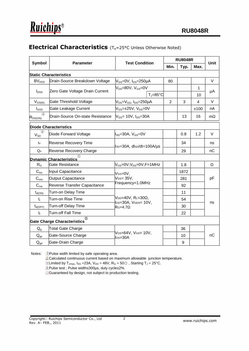
Electrical Characteristics (TA=25°C Unless Otherwise Noted)
RU8048RSymbol Parameter Test Condition
Min. Typ. Max.Unit
Static CharacteristicsBVDSS Drain-Source Breakdown Voltage VGS=0V, IDS=250µA 80 V
VDS=80V, VGS=0V 1IDSS Zero Gate Voltage Drain Current
TJ=85°C 10µA
VGS(th) Gate Threshold Voltage VDS=VGS, IDS=250µA 2 3 4 V
IGSS Gate Leakage Current VGS=±25V, VDS=0V ±100 nA
RDS(ON)④ Drain-Source On-state Resistance VGS= 10V, IDS=30A 13 16 mΩ
Notes: Pulse width limited by safe operating area.Calculated continuous current based on maximum allowable junction temperature.Limited by TJmax, IAS =23A, VDD = 48V, RG = 50Ω , Starting TJ = 25°C.Pulse test ; Pulse width≤300µs, duty cycle≤2%.Guaranteed by design, not subject to production testing.
Diode Characteristics
VSD④ Diode Forward Voltage ISD=30A, VGS=0V 0.8 1.2 V
trr Reverse Recovery Time 34 ns
Qrr Reverse Recovery ChargeISD=30A, dlSD/dt=100A/µs
29 nC
Dynamic Characteristics⑤
RG Gate Resistance VGS=0V,VDS=0V,F=1MHz 1.8 Ω
Ciss Input Capacitance 1872Coss Output Capacitance 281Crss Reverse Transfer Capacitance
VGS=0V,VDS= 35V,Frequency=1.0MHz 92
pF
td(ON) Turn-on Delay Time 11tr Turn-on Rise Time 54
td(OFF) Turn-off Delay Time 30tf Turn-off Fall Time
VDD=40V, RL=30Ω,IDS=30A, VGEN= 10V,RG=4.7Ω
22
ns
Gate Charge Characteristics⑤
Qg Total Gate Charge 36Qgs Gate-Source Charge 10Qgd Gate-Drain Charge
VDS=64V, VGS= 10V,IDS=30A
9
nC

Copyright Ruichips Semiconductor Co., LtdRev. A– FEB., 2011
3www.ruichips.com
RU8048R
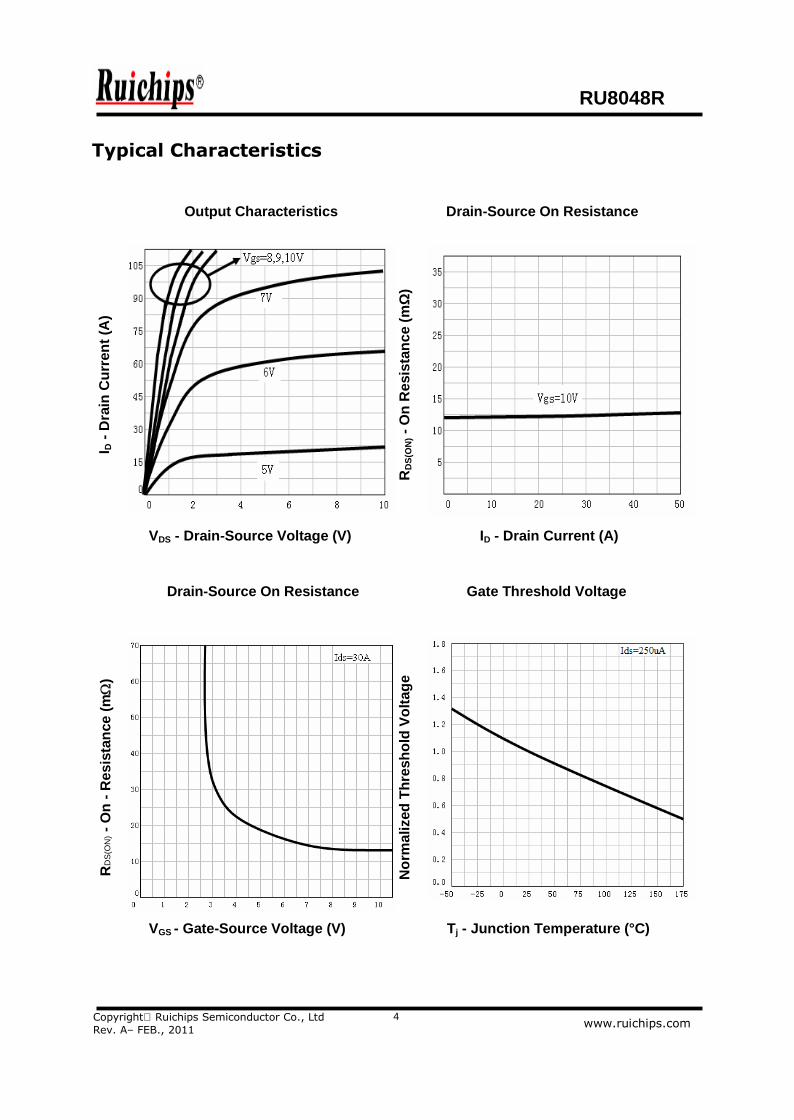
Typical Characteristics
Power Dissipation Drain Current
P tot
-Pow
er(W
)
I D- D
rain
Cur
rent
(A)
Tj - Junction Temperature (°C) Tj - Junction Temperature (°C)
Safe Operation Area Thermal Transient Impedance
I D- D
rain
Cur
rent
(A)
Nor
mal
ized
Effe
ctiv
e Tr
ansi
ent
VDS - Drain-Source Voltage (V) Square Wave Pulse Duration (sec)
Copyright Ruichips Semiconductor Co., LtdRev. A– FEB., 2011
4www.ruichips.com
RU8048R
Typical Characteristics
Output Characteristics Drain-Source On Resistance
I D- D
rain
Cur
rent
(A)
RD
S(O
N)- O
n R
esis
tanc
e (m
Ω)
VDS - Drain-Source Voltage (V) ID - Drain Current (A)
Drain-Source On Resistance Gate Threshold Voltage
RD
S(O
N)- O
n- R
esis
tanc
e (m
)
Nor
mal
ized
Thr
esho
ld V
olta
ge
VGS - Gate-Source Voltage (V) Tj - Junction Temperature (°C)

Copyright Ruichips Semiconductor Co., LtdRev. A– FEB., 2011
5www.ruichips.com
RU8048R
Typical Characteristics
Drain-Source On Resistance Source-Drain Diode Forward
Nor
mal
ized
On
Res
ista
nce
I S- S
ourc
e C
urre
nt (A
)
Tj - Junction Temperature (°C) VSD - Source-Drain Voltage (V)
Capacitance Gate Charge
C- C
apac
itanc
e (p
F)
V GS
- Gat
e-So
urce
Vol
tage
(V)
VDS - Drain-Source Voltage (V) QG - Gate Charge (nC)

Copyright Ruichips Semiconductor Co., LtdRev. A– FEB., 2011
6www.ruichips.com
RU8048R
Avalanche Test Circuit and Waveforms
Switching Time Test Circuit and Waveforms
Copyright Ruichips Semiconductor Co., LtdRev. A– FEB., 2011
7www.ruichips.com
RU8048R
Ordering and Marking Information
RU8048Package (Available)
R : TO220Operating Temperature Range
C : -55 to 175 ºCAssembly Material
G : Green & Lead FreePackaging
T : TUBE

Copyright Ruichips Semiconductor Co., LtdRev. A– FEB., 2011
8www.ruichips.com
RU8048R
Package Information
TO-220FB-3L
ALL DIMENSIONS REFER TO JEDEC STANDARDDO NOT INCLUDE MOLD FLASH OR PROTRUSIONS
MM INCH MM INCHSYMBOL
MIN NOM MAX MIN NOM MAXSYMBOL
MIN NOM MAX MIN NOM MAX
A 4.40 4.57 4.70 0.173 0.180 0.185 Øp1 1.40 1.50 1.60 0.055 0.059 0.063
A1 1.27 1.30 1.33 0.050 0.051 0.052 e 2.54BSC 0.1BSC
A2 2.35 2.40 2.50 0.093 0.094 0.098 e1 5.08BSC 0.2BSC
b 0.77 - 0.90 0.030 - 0.035 H1 6.40 6.50 6.60 0.252 0.256 0.260
b2 1.23 - 1.36 0.048 - 0.054 L 12.75 - 13.17 0.502 - 0.519
C 0.48 0.50 0.52 0.019 0.020 0.021 L1 - - 3.95 - - 0.156
D 15.40 15.60 15.80 0.606 0.614 0.622 L2 2.50REF. 0.098REF.
D1 9.00 9.10 9.20 0.354 0.358 0.362 Øp 3.57 3.60 3.63 0.141 0.142 0.143
DEP 0.05 0.10 0.20 0.002 0.004 0.008 Q 2.73 2.80 2.87 0.107 0.110 0.113
E 9.70 9.90 10.10 0.382 0.389 0.398 θ1 5° 7° 9° 5° 7° 9°
E1 - 8.70 - - 0.343 - θ2 1° 3° 5° 1° 3° 5°
E2 9.80 10.00 10.20 0.386 0.394 0.401
Copyright Ruichips Semiconductor Co., LtdRev. A– FEB., 2011
9www.ruichips.com
RU8048R
Customer Service
Worldwide Sales and Service:[email protected]
Technical Support:[email protected]
Investor Relations Contacts:[email protected]
Marcom Contact:[email protected]
Editorial Contact:[email protected]
HR Contact:[email protected]
Legal Contact:[email protected]
Shen Zhen RUICHIPS Semiconductor CO., LTDRoom 501, the 5floor An Tong Industrial Building,NO.207 Mei Hua Road Fu Tian Area Shen Zhen City, CHINA
TEL: (86-755) 8311-5334FAX: (86-755) 8311-4278E-mail: [email protected]


![SKC32.61 Datasheet en[1]](https://static.fdocuments.net/doc/165x107/544dd02daf7959f3138b5162/skc3261-datasheet-en1.jpg)