Data Sheet ADP3654 · 10 ns typical rise time and fall time at 2.2 nF load . Matched propagation...
14
High Speed, Dual, 4 A MOSFET Driver Data Sheet ADP3654 Rev. A Document Feedback Information furnished by Analog Devices is believed to be accurate and reliable. However, no responsibility is assumed by Analog Devices for its use, nor for any infringements of patents or other rights of third parties that may result from its use. Specifications subject to change without notice. No license is granted by implication or otherwise under any patent or patent rights of Analog Devices. Trademarks and registered trademarks are the property of their respective owners. One Technology Way, P.O. Box 9106, Norwood, MA 02062-9106, U.S.A. Tel: 781.329.4700 ©2010–2015 Analog Devices, Inc. All rights reserved. Technical Support www.analog.com FEATURES Industry-standard-compatible pinout High current drive capability Precise UVLO comparator with hysteresis 3.3 V-compatible inputs 10 ns typical rise time and fall time at 2.2 nF load Matched propagation delays between channels Fast propagation delay 4.5 V to 18 V supply voltage Parallelable dual outputs Rated from −40°C to +125°C junction temperature Thermally enhanced packages, 8-lead SOIC_N_EP and 8-lead MINI_SO_EP APPLICATIONS AC-to-dc switch mode power supplies DC-to-dc power supplies Synchronous rectification Motor drives GENERAL DESCRIPTION The ADP3654 high current and dual high speed driver is capable of driving two independent N-channel power MOSFETs. The driver uses the industry-standard footprint but adds high speed switching performance. The wide input voltage range allows the driver to be compatible with both analog and digital PWM controllers. Digital power controllers are powered from a low voltage supply, and the driver is powered from a higher voltage supply. The ADP3654 driver adds UVLO and hysteresis functions, allowing safe startup and shutdown of the higher voltage supply when used with low voltage digital controllers. The driver is available in thermally enhanced SOIC_N_EP and MINI_SO_EP packaging to maximize high frequency and current switching in a small printed circuit board (PCB) area. FUNCTIONAL BLOCK DIAGRAM 7 6 5 ADP3654 OUTA VDD OUTB 8 NC V DD UVLO 2 3 4 INA PGND INB 1 NC 09054-001 Figure 1.
Transcript of Data Sheet ADP3654 · 10 ns typical rise time and fall time at 2.2 nF load . Matched propagation...

High Speed, Dual, 4 A MOSFET Driver
Data Sheet ADP3654
Rev. A Document Feedback Information furnished by Analog Devices is believed to be accurate and reliable. However, no responsibility is assumed by Analog Devices for its use, nor for any infringements of patents or other rights of third parties that may result from its use. Specifications subject to change without notice. No license is granted by implication or otherwise under any patent or patent rights of Analog Devices. Trademarks and registered trademarks are the property of their respective owners.
One Technology Way, P.O. Box 9106, Norwood, MA 02062-9106, U.S.A. Tel: 781.329.4700 ©2010–2015 Analog Devices, Inc. All rights reserved. Technical Support www.analog.com
FEATURES Industry-standard-compatible pinout High current drive capability Precise UVLO comparator with hysteresis 3.3 V-compatible inputs 10 ns typical rise time and fall time at 2.2 nF load Matched propagation delays between channels Fast propagation delay 4.5 V to 18 V supply voltage Parallelable dual outputs Rated from −40°C to +125°C junction temperature Thermally enhanced packages, 8-lead SOIC_N_EP and 8-lead
MINI_SO_EP
APPLICATIONS AC-to-dc switch mode power supplies DC-to-dc power supplies Synchronous rectification Motor drives
GENERAL DESCRIPTION The ADP3654 high current and dual high speed driver is capable of driving two independent N-channel power MOSFETs. The driver uses the industry-standard footprint but adds high speed switching performance.
The wide input voltage range allows the driver to be compatible with both analog and digital PWM controllers.
Digital power controllers are powered from a low voltage supply, and the driver is powered from a higher voltage supply. The ADP3654 driver adds UVLO and hysteresis functions, allowing safe startup and shutdown of the higher voltage supply when used with low voltage digital controllers.
The driver is available in thermally enhanced SOIC_N_EP and MINI_SO_EP packaging to maximize high frequency and current switching in a small printed circuit board (PCB) area.
FUNCTIONAL BLOCK DIAGRAM
7
6
5
ADP3654
OUTA
VDD
OUTB
8 NCVDD
UVLO
2
3
4
INA
PGND
INB
1NC09
054-
001
Figure 1.
ADP3654* Product Page Quick LinksLast Content Update: 11/01/2016
Comparable PartsView a parametric search of comparable parts
DocumentationData Sheet• ADP3654: High Speed, Dual, 4 A MOSFET Driver
Design Resources• ADP3654 Material Declaration• PCN-PDN Information• Quality And Reliability• Symbols and Footprints
DiscussionsView all ADP3654 EngineerZone Discussions
Sample and BuyVisit the product page to see pricing options
Technical SupportSubmit a technical question or find your regional support number
* This page was dynamically generated by Analog Devices, Inc. and inserted into this data sheet. Note: Dynamic changes to the content on this page does not constitute a change to the revision number of the product data sheet. This content may be frequently modified.

ADP3654 Data Sheet
Rev. A | Page 2 of 13
TABLE OF CONTENTS Features .............................................................................................. 1 Applications ....................................................................................... 1 General Description ......................................................................... 1 Functional Block Diagram .............................................................. 1 Revision History ............................................................................... 2 Specifications ..................................................................................... 3
Timing Diagrams .......................................................................... 3 Absolute Maximum Ratings ............................................................ 4
ESD Caution .................................................................................. 4 Pin Configuration and Function Descriptions ............................. 5 Typical Performance Characteristics ............................................. 6
Test Circuit .........................................................................................8 Theory of Operation .........................................................................9
Input Drive Requirements (INA and INB) ................................9 Low-Side Drivers (OUTA, OUTB) .............................................9 Supply Capacitor Selection ..........................................................9 PCB Layout Considerations .........................................................9 Parallel Operation ...................................................................... 10 Thermal Considerations ............................................................ 10
Outline Dimensions ....................................................................... 12 Ordering Guide .......................................................................... 13
REVISION HISTORY 8/15—Rev. 0 to Rev. A Changes to Figure 5 .......................................................................... 6 Updated Outline Dimensions ....................................................... 12 Changes to Ordering Guide .......................................................... 13 8/10—Revision 0: Initial Version
Data Sheet ADP3654
Rev. A | Page 3 of 13
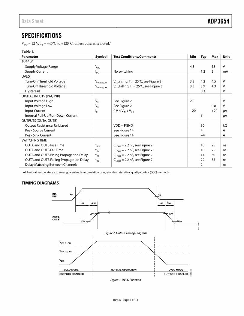
SPECIFICATIONS VDD = 12 V, TJ = −40°C to +125°C, unless otherwise noted.1
Table 1. Parameter Symbol Test Conditions/Comments Min Typ Max Unit SUPPLY
Supply Voltage Range VDD 4.5 18 V Supply Current IDD No switching 1.2 3 mA
UVLO Turn-On Threshold Voltage VUVLO_ON VDD rising, TJ = 25°C, see Figure 3 3.8 4.2 4.5 V Turn-Off Threshold Voltage VUVLO_OFF VDD falling, TJ = 25°C, see Figure 3 3.5 3.9 4.3 V Hysteresis 0.3 V
DIGITAL INPUTS (INA, INB) Input Voltage High VIH See Figure 2 2.0 V Input Voltage Low VIL See Figure 2 0.8 V Input Current IIN 0 V < VIN < VDD −20 +20 µA Internal Pull-Up/Pull-Down Current 6 µA
OUTPUTS (OUTA, OUTB) Output Resistance, Unbiased VDD = PGND 80 kΩ Peak Source Current See Figure 14 4 A Peak Sink Current See Figure 14 −4 A
SWITCHING TIME OUTA and OUTB Rise Time tRISE CLOAD = 2.2 nF, see Figure 2 10 25 ns OUTA and OUTB Fall Time tFALL CLOAD = 2.2 nF, see Figure 2 10 25 ns OUTA and OUTB Rising Propagation Delay tD1 CLOAD = 2.2 nF, see Figure 2 14 30 ns OUTA and OUTB Falling Propagation Delay tD2 CLOAD = 2.2 nF, see Figure 2 22 35 ns Delay Matching Between Channels 2 ns
1 All limits at temperature extremes guaranteed via correlation using standard statistical quality control (SQC) methods.
TIMING DIAGRAMS
INA,INB
OUTA,OUTB
tD1 tRISE
10%
90%
10%
90%
VIH VIL
tD2 tFALL
0905
4-00
2
Figure 2. Output Timing Diagram
NORMAL OPERATIONUVLO MODE
OUTPUTS DISABLED
VDD
VUVLO_ON
VUVLO_OFF
UVLO MODE
OUTPUTS DISABLED
0905
4-00
3
Figure 3. UVLO Function

ADP3654 Data Sheet
Rev. A | Page 4 of 13
ABSOLUTE MAXIMUM RATINGS Table 2. Parameter Rating VDD −0.3 V to +20 V OUTA, OUTB
DC −0.3 V to VDD + 0.3 V <200 ns −2 V to VDD + 0.3 V
INA, INB −0.3 V to VDD + 0.3 V ESD
Human Body Model (HBM) 3.5 kV Field Induced Charged Device Model (FICDM)
SOIC_N_EP 1.5 kV MINI_SO_EP 1.0 kV
θJA, JEDEC 4-Layer Board SOIC_N_EP1 59°C/W MINI_SO_EP1 43°C/W
Junction Temperature Range −40°C to +150°C Storage Temperature Range −65°C to +150°C Lead Temperature
Soldering (10 sec) 300°C Vapor Phase (60 sec) 215°C Infrared (15 sec) 260°C
1 θJA is measured per JEDEC standards, JESD51-2, JESD51-5, and JESD51-7, as
appropriate with the exposed pad soldered to the PCB.
Stresses at or above those listed under Absolute Maximum Ratings may cause permanent damage to the product. This is a stress rating only; functional operation of the product at these or any other conditions above those indicated in the operational section of this specification is not implied. Operation beyond the maximum operating conditions for extended periods may affect product reliability.
ESD CAUTION

Data Sheet ADP3654
Rev. A | Page 5 of 13
PIN CONFIGURATION AND FUNCTION DESCRIPTIONS
NC 1
INA 2
PGND 3
INB 4
NC8
OUTA7
VDD6
OUTB5
ADP3654TOP VIEW
(Not to Scale)
NOTES1. NC = NO CONNECT.2. THE EXPOSED PAD OF THE PACKAGE IS NOT DIRECTLY
CONNECTED TO ANY PIN OF THE PACKAGE, BUT IT ISELECTRICALLY AND THERMALLY CONNECTED TO THE DIESUBSTRATE, WHICH IS THE GROUND OF THE DEVICE. IT ISRECOMMENDED TO HAVE THE EXPOSED PAD AND THEPGND PIN CONNECTED ON THE PCB. 09
054-
004
Figure 4. Pin Configuration
Table 3. Pin Function Descriptions Pin No. Mnemonic Description 1 NC No Connect. 2 INA Input Pin for Channel A Gate Driver. 3 PGND Ground. This pin should be closely connected to the source of the power MOSFET. 4 INB Input Pin for Channel B Gate Driver. 5 OUTB Output Pin for Channel B Gate Driver. 6 VDD Power Supply Voltage. Bypass this pin to PGND with a ~1 µF to 5 µF ceramic capacitor. 7 OUTA Output Pin for Channel A Gate Driver. 8 NC No Connect. 9 EPAD Exposed Pad. The exposed pad of the package is not directly connected to any pin of the package, but it is
electrically and thermally connected to the die substrate, which is the ground of the device. It is recommended to have the exposed pad and the PGND pin connected on the PCB.

ADP3654 Data Sheet
Rev. A | Page 6 of 13
TYPICAL PERFORMANCE CHARACTERISTICS VDD = 12 V, TJ = 25°C, unless otherwise noted.
3
4
5
6
7
8
9
–50 –30 –10 10 30 50 70 90 110 130TEMPERATURE (°C)
UVL
O (V
)
VUVLO_ON
VUVLO_OFF09
054-
005
Figure 5. UVLO vs. Temperature
0
2
4
6
8
10
12
14
–50 –30 –10 10 30 50 70 90 110 130TEMPERATURE (°C)
tFALL
tRISE
TIM
E (n
s)
0905
4-00
6
Figure 6. Rise and Fall Times vs. Temperature
0
10
20
30
40
50
60
–50 –30 –10 10 30 50 70 90 110 130TEMPERATURE (°C)
TIM
E (n
s)
VDD = 12V
tD2
tD1
0905
4-00
7
Figure 7. Propagation Delay vs. Temperature
0
5
10
15
20
25
0 5 10 15 20VDD (V)
TIM
E (n
s)
tFALL
tRISE
0905
4-00
8
Figure 8. Rise and Fall Times vs. VDD
0
10
20
30
40
50
60
70
0 5 10 15 20
tD2
tD1
VDD (V)
TIM
E (n
s)
0905
4-00
9
Figure 9. Propagation Delay vs. VDD
1
2
OUTA/OUTB
INA/INB
VDD = 12VTIME = 20ns/DIV
0905
4-01
0
Figure 10. Typical Rise Propagation Delay

Data Sheet ADP3654
Rev. A | Page 7 of 13
1
2
VDD = 12VTIME = 20ns/DIV
OUTA/OUTB
INA/INB
0905
4-01
1
Figure 11. Typical Fall Propagation Delay
1
2
VDD = 12VTIME = 20ns/DIV
OUTA/OUTB
INA/INB
0905
4-01
2
Figure 12. Typical Rise Time
1
2
VDD = 12VTIME = 20ns/DIV
OUTA/OUTB
INA/INB
0905
4-01
3
Figure 13. Typical Fall Time
ADP3654 Data Sheet
Rev. A | Page 8 of 13
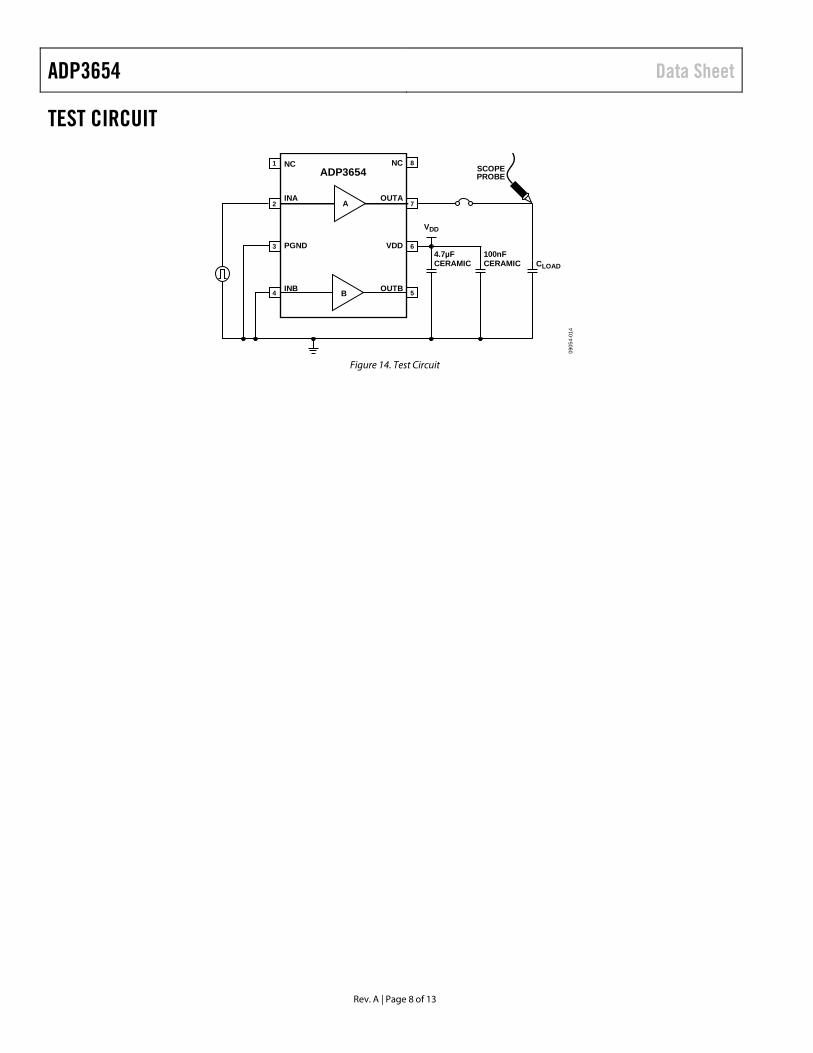
TEST CIRCUIT
INA
VDD
VDD
PGND
ADP3654
OUTA
OUTBINB
NC NC1
3
8
7
6
5
A
B
2
4
CLOAD100nFCERAMIC
4.7µFCERAMIC
SCOPEPROBE
0905
4-01
4
Figure 14. Test Circuit

Data Sheet ADP3654
Rev. A | Page 9 of 13
THEORY OF OPERATION The ADP3654 dual driver is optimized for driving two independent enhancement N-channel MOSFETs or insulated gate bipolar transistors (IGBTs) in high switching frequency applications.
These applications require high speed, fast rise and fall times, as well as short propagation delays. The capacitive nature of the aforementioned gated devices requires high peak current capability as well.
INA
VDD
VDD
PGND
ADP3654
OUTA
OUTBINB
NC NC1
3
8
7
6
5
A
B
2
4
VDS
VDS
0905
4-01
5
Figure 15. Typical Application Circuit
INPUT DRIVE REQUIREMENTS (INA AND INB) The ADP3654 is designed to meet the requirements of modern digital power controllers; the signals are compatible with 3.3 V logic levels. At the same time, the input structure allows for input voltages as high as VDD.
An internal pull-down resistor is present at the input, which guarantees that the power device is off in the event that the input is left floating.
LOW-SIDE DRIVERS (OUTA, OUTB) The ADP3654 dual drivers are designed to drive ground referenced N-channel MOSFETs. The bias is internally connected to the VDD supply and PGND.
When ADP3654 is disabled, both low-side gates are held low. Internal impedance is present between the OUTA pin and GND and between the OUTB pin and GND; this feature ensures that the power MOSFET is normally off when bias voltage is not present.
When interfacing ADP3654 to external MOSFETs, the designer should consider ways to make a robust design that minimizes stresses on both the driver and the MOSFETs. These stresses include exceeding the short time duration voltage ratings on the OUTA and OUTB pins, as well as the external MOSFET.
Power MOSFETs are usually selected to have a low on resistance to minimize conduction losses, which usually implies a large input gate capacitance and gate charge.
SUPPLY CAPACITOR SELECTION For the supply input (VDD) of the ADP3654, a local bypass capacitor is recommended to reduce the noise and to supply some of the peak currents that are drawn.
An improper decoupling can dramatically increase the rise times because excessive resonance on the OUTA and OUTB pins can, in some extreme cases, damage the device, due to inductive overvoltage on the VDD, OUTA, or OUTB pin.
The minimum capacitance required is determined by the size of the gate capacitances being driven, but as a general rule, a 4.7 µF, low ESR capacitor should be used. Multilayer ceramic chip (MLCC) capacitors provide the best combination of low ESR and small size. Use a smaller ceramic capacitor (100 nF) with a better high frequency characteristic in parallel to the main capacitor to further reduce noise.
Keep the ceramic capacitor as close as possible to the ADP3654 device and minimize the length of the traces going from the capacitor to the power pins of the device.
PCB LAYOUT CONSIDERATIONS Use the following general guidelines when designing PCBs:
• Trace out the high current paths and use short, wide (>40 mil) traces to make these connections.
• Minimize trace inductance between the OUTA and OUTB outputs and MOSFET gates.
• Connect the PGND pin of the ADP3654 device as closely as possible to the source of the MOSFETs.
• Place the VDD bypass capacitor as close as possible to the VDD and PGND pins.
• Use vias to other layers, when possible, to maximize thermal conduction away from the IC.

ADP3654 Data Sheet
Rev. A | Page 10 of 13
Figure 16 shows an example of the typical layout based on the preceding guidelines.
0905
4-01
6
Figure 16. External Component Placement Example
Note that the exposed pad of the package is not directly con-nected to any pin of the package, but it is electrically and thermally connected to the die substrate, which is the ground of the device.
PARALLEL OPERATION The two driver channels present in the ADP3654 device can be combined to operate in parallel to increase drive capability and minimize power dissipation in the driver.
The connection scheme is shown in Figure 17. In this configura-tion, INA and INB are connected together, and OUTA and OUTB are connected together.
Particular attention must be paid to the layout in this case to optimize load sharing between the two drivers.
INA
VDD
VDD
PGND
ADP3654
OUTA
OUTBINB
NC NC1
3
8
7
6
5
A
B
2
4
VDS
0905
4-01
7
Figure 17. Parallel Operation
THERMAL CONSIDERATIONS When designing a power MOSFET gate drive, the maximum power dissipation in the driver must be considered to avoid exceeding maximum junction temperature.
Data on package thermal resistance is provided in Table 2 to help the designer with this task.
There are several equally important aspects that must be considered, such as the following:
• Gate charge of the power MOSFET being driven • Bias voltage value used to power the driver • Maximum switching frequency of operation • Value of external gate resistance • Maximum ambient (and PCB) temperature • Type of package
All of these factors influence and limit the maximum allowable power dissipated in the driver.
The gate of a power MOSFET has a nonlinear capacitance characteristic. For this reason, although the input capacitance is usually reported in the MOSFET data sheet as CISS, it is not useful to calculate power losses.
The total gate charge necessary to turn on a power MOSFET device is usually reported on the device data sheet under QG. This parameter varies from a few nanocoulombs (nC) to several hundred nC, and is specified at a specific VGS value (10 V or 4.5 V).
The power necessary to charge and then discharge the gate of a power MOSFET can be calculated as:
PGATE = VGS × QG × fSW
where: VGS is the bias voltage powering the driver (VDD). QG is the total gate charge. fSW is the maximum switching frequency.
The power dissipated for each gate (PGATE) still needs to be multiplied by the number of drivers (in this case, 1 or 2) being used in each package, and it represents the total power dissi-pated in charging and discharging the gates of the power MOSFETs.
Not all of this power is dissipated in the gate driver because part of it is actually dissipated in the external gate resistor, RG. The larger the external gate resistor is, the smaller the amount of power that is dissipated in the gate driver.
In modern switching power applications, the value of the gate resistor is kept at a minimum to increase switching speed and minimize switching losses.
In all practical applications where the external resistor is in the order of a few ohms, the contribution of the external resistor can be neglected, and the extra loss is assumed in the driver, providing a good guard band to the power loss calculations.

Data Sheet ADP3654
Rev. A | Page 11 of 13
In addition to the gate charge losses, there are also dc bias losses, due to the bias current of the driver. This current is present regardless of the switching.
PDC = VDD × IDD
The total estimated loss is the sum of PDC and PGATE.
PLOSS = PDC + (n × PGATE)
where n is the number of gates driven.
When the total power loss is calculated, the temperature increase can be calculated as
ΔTJ = PLOSS × θJA
Design Example
For example, consider driving two IRFS4310Z MOSFETs with a VDD of 12 V at a switching frequency of 300 kHz, using an ADP3654 in the SOIC_N_EP package.
The maximum PCB temperature considered for this design is 85°C.
From the MOSFET data sheet, the total gate charge is QG = 120 nC.
PGATE = 12 V × 120 nC × 300 kHz = 432 mW
PDC = 12 V × 1.2 mA = 14.4 mW
PLOSS = 14.4 mW + (2 × 432 mW) = 878.4 mW
The SOIC_N_EP thermal resistance is 59°C/W.
ΔTJ = 878.4 mW × 59°C/W = 51.8°C
TJ = TA + ΔTJ = 136.8°C ≤ TJMAX
This estimated junction temperature does not factor in the power dissipated in the external gate resistor and, therefore, provides a certain guard band.
If a lower junction temperature is required by the design, the MINI_SO_EP package can be used, which provides a thermal resistance of 43°C/W, so that the maximum junction temperature is
ΔTJ = 878.4 mW × 43°C/W = 37.7°C
TJ = TA + ΔTJ = 122.7°C ≤ TJMAX
Other options to reduce power dissipation in the driver include reducing the value of the VDD bias voltage, reducing switching fre-quency, and choosing a power MOSFET with smaller gate charge.

ADP3654 Data Sheet
Rev. A | Page 12 of 13
OUTLINE DIMENSIONS
COMPLIANT TO JEDEC STANDARDS MS-012-AA 06-0
2-20
11-B
1.270.40
1.751.35
2.29
2.29
0.356
0.457
4.003.903.80
6.206.005.80
5.004.904.80
0.10 MAX0.05 NOM
3.81 REF
0.250.17
8°0°
0.500.25
45°
COPLANARITY0.10
1.04 REF
8
1 4
5
1.27 BSC
SEATINGPLANE
FOR PROPER CONNECTION OFTHE EXPOSED PAD, REFER TOTHE PIN CONFIGURATION ANDFUNCTION DESCRIPTIONSSECTION OF THIS DATA SHEET.
BOTTOM VIEW
TOP VIEW
0.510.31
1.651.25
Figure 18. 8-Lead Standard Small Outline Package, with Exposed Pad [SOIC_N_EP]
Narrow Body (RD-8-1) Dimensions shown in millimeters
0710
08-A
COMPLIANT TO JEDEC STANDARDS MO-187-AA-T
0.700.550.40
8°0°
0.940.860.78
SEATINGPLANE
1.10 MAX
0.150.100.05
0.400.330.25
5.054.904.75
2.262.162.06
1.831.731.63
3.103.002.90
3.103.002.90
8 5
41
0.65 BSC0.525 BSC
PIN 1INDICATOR
COPLANARITY0.10
0.230.180.13
TOPVIEW
BOTTOM VIEW
EXPOSEDPAD
FOR PROPER CONNECTION OFTHE EXPOSED PAD, REFER TOTHE PIN CONFIGURATION ANDFUNCTION DESCRIPTIONSSECTION OF THIS DATA SHEET.
Figure 19. 8-Lead Mini Small Outline Package with Exposed Pad [MINI_SO_EP]
(RH-8-1) Dimensions shown in millimeters

Data Sheet ADP3654
Rev. A | Page 13 of 13
ORDERING GUIDE
Model1 UVLO Option
Temperature Range Package Description
Package Option
Ordering Quantity Branding
ADP3654ARDZ 4.5 V −40°C to +125°C 8-Lead Standard Small Outline Package (SOIC_N_EP), Tube
RD-8-1 98
ADP3654ARDZ-R7 4.5 V −40°C to +125°C 8-Lead Standard Small Outline Package (SOIC_N_EP), 7“ Tape and Reel
RD-8-1 1,000
ADP3654ARDZ-RL 4.5 V −40°C to +125°C 8-Lead Standard Small Outline Package (SOIC_N_EP), 13“ Tape and Reel
RD-8-1 2,500
ADP3654ARHZ 4.5 V −40°C to +125°C 8-Lead Mini Small Outline Package (MINI_SO_EP), Tube
RH-8-1 50 78
ADP3654ARHZ-R7 4.5 V −40°C to +125°C 8-Lead Mini Small Outline Package (MINI_SO_EP), 7“ Tape and Reel)
RH-8-1 1,000 78
ADP3654ARHZ-RL 4.5 V −40°C to +125°C 8-Lead Mini Small Outline Package (MINI_SO_EP), 13” Tape and Reel
RH-8-1 3,000 78
1 Z = RoHS Compliant Part.
©2010–2015 Analog Devices, Inc. All rights reserved. Trademarks and registered trademarks are the property of their respective owners. D09054-0-8/15(A)