Czochralski Silicon - a radiation hard material? Vertex 2005 November 7 – 11 Chuzenji Lake, Japan...
42
Czochralski Silicon - a radiation hard material? Vertex 2005 November 7 – 11 Chuzenji Lake, Japan Alison Bates The University of Glasgow, UK.
-
Upload
annabelle-nancy-allison -
Category
Documents
-
view
214 -
download
1
Transcript of Czochralski Silicon - a radiation hard material? Vertex 2005 November 7 – 11 Chuzenji Lake, Japan...
Czochralski Silicon- a radiation hard
material?
Vertex 2005 November 7 – 11
Chuzenji Lake, Japan
Alison BatesThe University of Glasgow, UK.
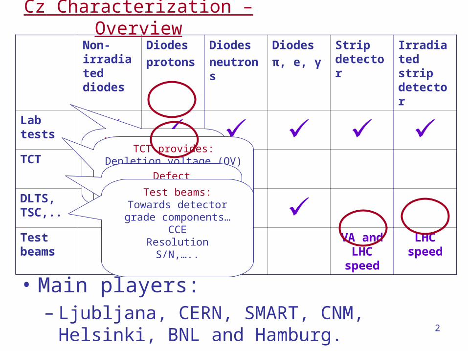
2
• Main players:– Ljubljana, CERN, SMART, CNM, Helsinki,
BNL and Hamburg.
Cz Characterization – Overview
Non-irradiated diodes
Diodes
protons
Diodes
neutrons
Diodes
π, e, γ
Strip detector
Irradiated strip detector
Lab tests TCT DLTS, TSC,.. Test beams
VA and LHC
speed
LHC speed
Lab measurements study:CVIV
Annealing studies
TCT provides:Depletion voltage (QV)
CCESpace charge determination
Electric field profileTrapping times
Defect characterization:Specific defect level
concentrationsTest beams:
Towards detector grade components…
CCEResolution
S/N,…..
3
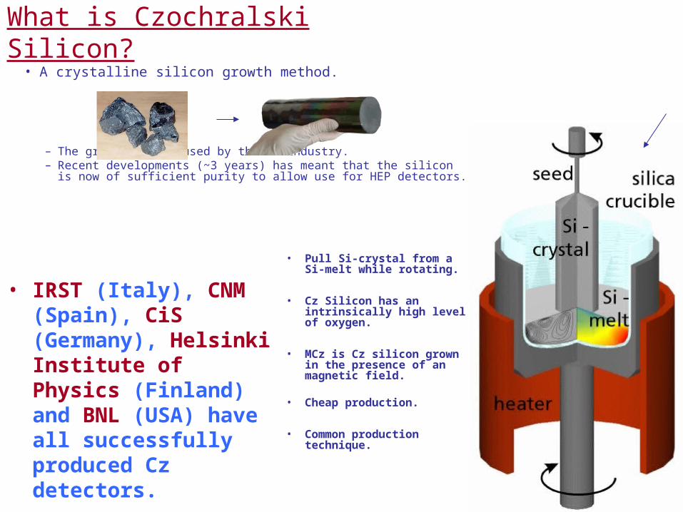
• A crystalline silicon growth method.
– The growth method used by the IC industry. – Recent developments (~3 years) has meant that the silicon is
now of sufficient purity to allow use for HEP detectors.
• Pull Si-crystal from a Si-melt while rotating.
• Cz Silicon has an intrinsically high level of oxygen.
• MCz is Cz silicon grown in the presence of an magnetic field.
• Cheap production.
• Common production technique.
Czochralski Growth
What is Czochralski Silicon?
• IRST (Italy), CNM (Spain), CiS (Germany), Helsinki Institute of Physics (Finland) and BNL (USA) have all successfully produced Cz detectors.

4
Float Zone silicon (FZ)-the usual growth method used to make HEP detectors
Single crystal silicon
Poly silicon
RF Heating coil
Float Zone Growth
• Start with a polysilicon rod inside a chamber either in a vacuum or an inert gas
• An RF heating coil melts ≈2 cm zone in the rod
• The RF coil moves through the rod, moving the molten silicon region with it
• This melting purifies the silicon rod
• Oxygen can be diffused into the silicon – called Diffusion Oxygenated Float Zone (DOFZ) (done at the wafer level)

5
• O in Diffusion Oxygenated FZ (DOFZ) ~ 1x1017 cm-3
• O in magnetic Cz (MCz) ~ 2-5 x1017 cm-3
Why should Cz be any better? - Oxygen is important
• DOFZ: Saturation of reverse annealing
(24 GeV/c p - only little effect after neutron irradiation observed !)
• DOFZ silicon has less variation in Vfd with radiation compared to FZ – more radiation hard
• Adding carbon to silicon decreases the radiation hardness
For hadron radiation only
0 1 2 3 4 524 GeV/c proton [1014 cm-2]
0
2
4
6
8
10
|Nef
f| [
1012
cm-3
]100
200
300
400
500
600
Vde
p [V
] (3
00 m
)
Carbon-enriched (P503)Standard (P51)
O-diffusion 24 hours (P52)O-diffusion 48 hours (P54)O-diffusion 72 hours (P56)
Carbonated
Standard
Oxygenated

6
• DOFZ: Saturation of reverse annealing
(24 GeV/c p - only little effect after neutron irradiation observed !)
0 2.1014 4.1014 6.1014 8.1014 1015
p [p/cm2]
0.0
0.5
1.0
1.5
2.0
NY [1
013/c
m3 ]
200
400
600
800
1000
Vde
p [V
] (2
80 m
)standard standard
DOFZ 24h/1150oCDOFZ 24h/1150oC
DOFZ 72h/1150oCDOFZ 72h/1150oC
20 GeV/c proton irradiation
[G.Lindstroem et al.]
1 10 100 1000 10000annealing time at 60oC [min]
0
2
4
6
8
10
N
eff [
1011
cm-3
]
NC
NC0
gC eq
NA NA NY
[M.Moll]
Reverse Annealing Component
Why should Cz be any better? - Oxygen is important
• O in Diffusion Oxygenated FZ (DOFZ) ~ 1x1017 cm-3
• O in magnetic Cz (MCz) ~ 2-5 x1017 cm-3
• DOFZ silicon has less variation in Vfd with radiation compared to FZ – more radiation hard
• Adding carbon to silicon decreases the radiation hardness
For hadron radiation only

7
Cz Characterization – leakage current
300μm thick 5x5 mm2 p+n silicon diodes (all 1 kΩcm) have been characterized before and after 24 GeV/c proton irradiation at the CERN PS.
Diodes processed at the Helsinki Institute of Physics from FZ, DOFZ and MCz silicon manufactured at Okmetric Oyj.
Silicon type α [A/cm]
FZ 4.96 x 10⁻¹⁷
DOFZ 4.85 x 10⁻¹⁷
MCz 4.73 x 10⁻¹⁷
The leakage current of MCz silicon after proton irradiation follows the same behaviour as FZ and DOFZ silicon
1012 1013 1014 1015
eq [ cm-2 ]
10-4
10-3
10-2
10-1
Nor
mal
ised
Cur
rent
[A
/cm
3 ]
FZ (f2)DOFZ (W317)DOFZ (d1)MCZ (n320)
4 min at 80oC
[A.G.Bates and M.Moll, to be published in NIMA]
8
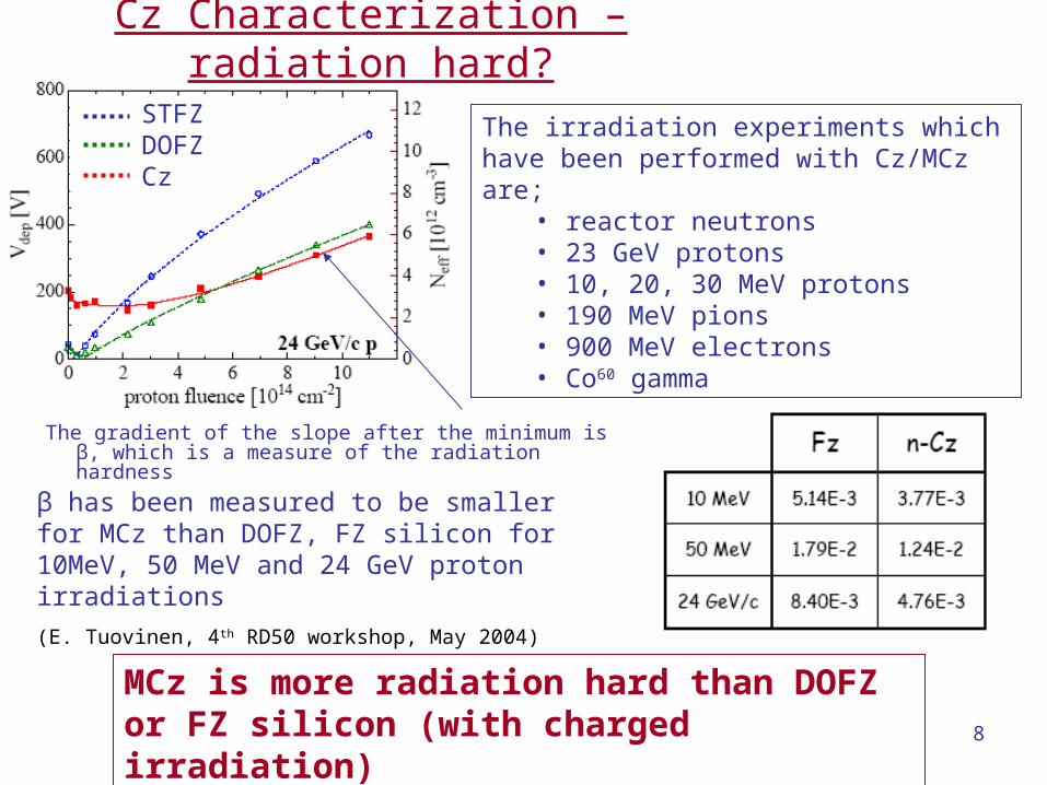
The gradient of the slope after the minimum is β, which is a measure of the radiation hardness
Cz Characterization – radiation hard?
β has been measured to be smaller for MCz than DOFZ, FZ silicon for 10MeV, 50 MeV and 24 GeV proton irradiations
(E. Tuovinen, 4th RD50 workshop, May 2004)
MCz is more radiation hard than DOFZ or FZ silicon (with charged irradiation)
The irradiation experiments which have been performed with Cz/MCz are;
• reactor neutrons• 23 GeV protons• 10, 20, 30 MeV protons• 190 MeV pions• 900 MeV electrons• Co60 gamma
STFZDOFZCz
9
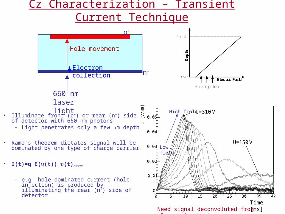
• Illuminate front (p+) or rear (n+) side of detector with 660 nm photons– Light penetrates only a few m depth
• Ramo’s theorem dictates signal will be dominated by one type of charge carrier
• I(t)=q E((t)) (t)drift
– e.g. hole dominated current (hole injection) is produced by illuminating the rear (n+) side of detector
660 nm laser light
p+
n+
Hole movement
Electron collection
Electric Field
De
pth
Front
rear
Hole injection
Low field
High field
Cz Characterization – Transient Current Technique
t[ns]0 5 10 15 20 25 30 35 40
]I
[V/5
0
0
0.01
0.02
0.03
0.04
0.05
U=150V
U=310V
Time [ns]Need signal deconvoluted from electronic shaping

10
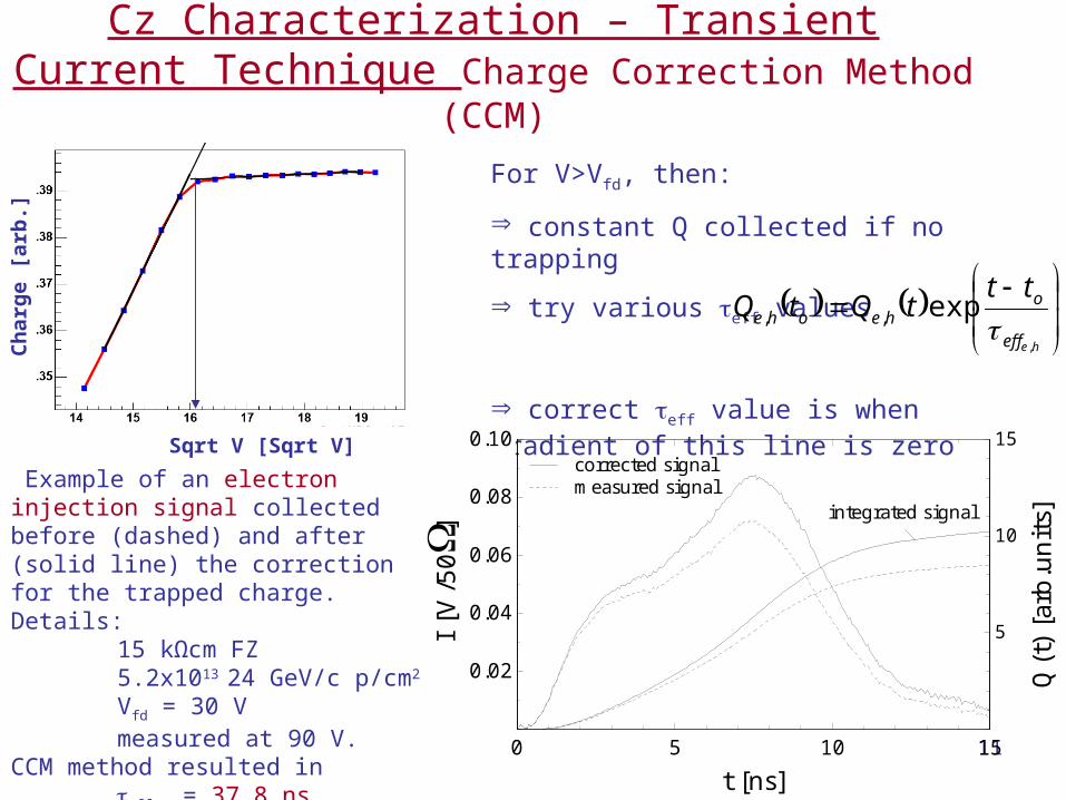
Cz Characterization – Transient Current Technique
When the detector has been irradiated the drifting charge, Qe,h(t), will be lost with an exponential time dependence due to trapping in the defects
To derive the electric field profile/SC sign you must take trapping effects into account
The effective trapping probability, 1/eff, is the probability that a carrier is lost due to trapping in the silicon.
))(
exp()()(,
,,
heeff
oohehe
tttQtQ
Injection timeInjection charge
heeff
oheohe
tttQtQ
,
exp,,
Measured charge from detector
Corrected charge
Trapping compensation
11
For V>Vfd, then:
constant Q collected if no trapping
try various eff values
correct eff value is when gradient of this line is zero
Ch
arg
e [
arb
.]
Sqrt V [Sqrt V]
Cz Characterization – Transient Current Technique Charge Correction Method (CCM)
0 5 10 15t [ns]
0.02
0.04
0.06
0.08
0.10I
[V/5
0]
5
10
15
Q(t
) [a
rb.u
nits
]
corrected signalmeasured signal
integrated signal Example of an electron injection signal collected before (dashed) and after (solid line) the correction for the trapped charge. Details:
15 kΩcm FZ 5.2x10¹³ 24 GeV/c p/cm2 Vfd = 30 Vmeasured at 90 V.
CCM method resulted in eff,e = 37.8 ns.
heeff
oheohe
tttQtQ
,
exp,,
12
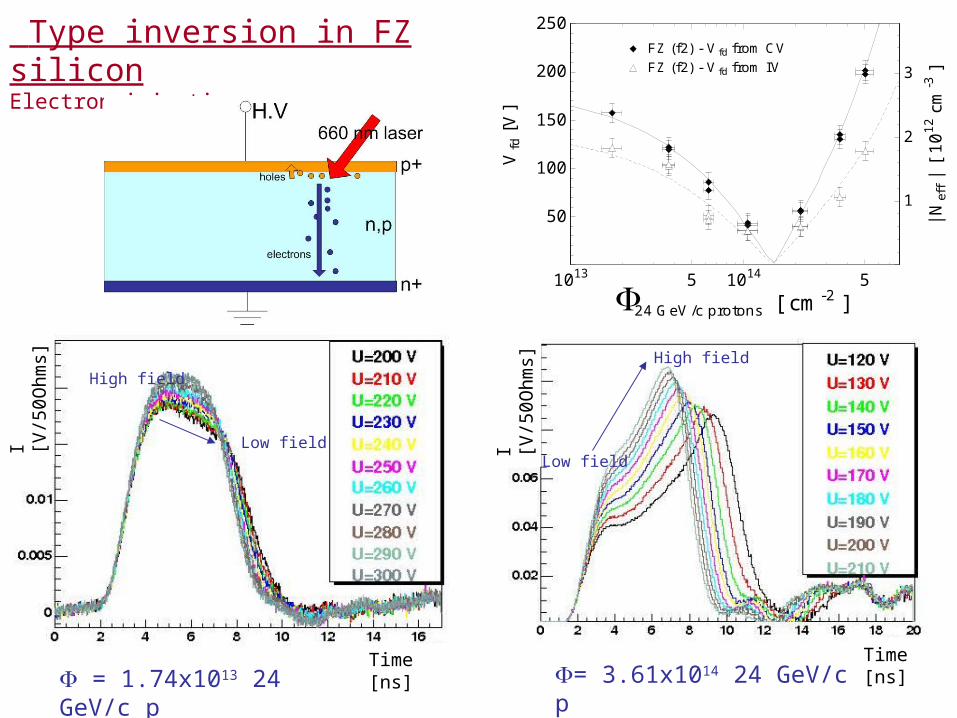
Type inversion in FZ siliconElectron injection
= 1.74x10¹³ 24 GeV/c p = 3.61x10¹⁴ 24 GeV/c p
Low fieldLow field
High fieldHigh field
Time [ns] Time [ns]
I [V
/50O
hms]
I [V
/50O
hms]
1013 5 1014 524 GeV/c protons [ cm-2 ]
50
100
150
200
250
Vfd
[V]
1
2
3
| Nef
f | [
1012
cm
-3 ]
FZ (f2) - Vfd from CVFZ (f2) - Vfd from IV
13
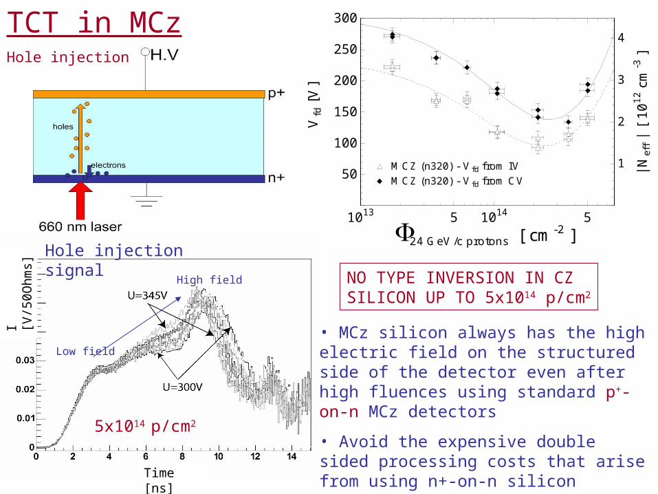
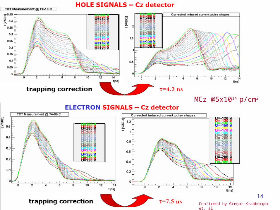
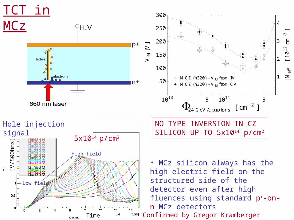
TCT in MCzHole injection
• MCz silicon always has the high electric field on the structured side of the detector even after high fluences using standard p+-on-n MCz detectors
• Avoid the expensive double sided processing costs that arise from using n+-on-n silicon detectors
14
Alison BatesTime [ns]
I [V
/50O
hms]
Low field
High field NO TYPE INVERSION IN CZ SILICON UP TO 5x10¹⁴ p/cm2
Hole injection signal
1013 5 1014 524 GeV/c protons [ cm-2 ]
50
100
150
200
250
300
Vfd
[V]
1
2
3
4
| Nef
f | [
1012
cm
-3 ]
MCZ (n320) - Vfd from IVMCZ (n320) - Vfd from CV
5x10¹⁴ p/cm2
14
MCz @5x10¹⁴ p/cm2
Confirmed by Gregor Kramberger et. al
15
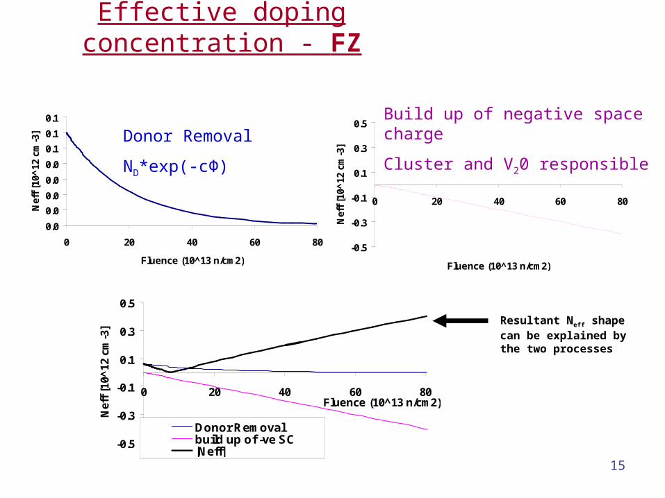
Effective doping concentration - FZ
0.0
0.0
0.0
0.0
0.0
0.1
0.1
0.1
0 20 40 60 80
Fluence (10^13 n/cm2)
Nef
f [1
0^12
cm
-3]
-0.5
-0.3
-0.1
0.1
0.3
0.5
0 20 40 60 80
Fluence (10^13 n/cm2)
Nef
f [1
0^12
cm
-3]
-0.5
-0.3
-0.1
0.1
0.3
0.5
0 20 40 60 80Fluence (10^13 n/cm2)
Nef
f [1
0^12
cm
-3]
Donor Removalbuild up of -ve SC|Neff|
Donor Removal
ND*exp(-cΦ)
Build up of negative space charge
Cluster and V20 responsible
Resultant Neff shape can be explained by the two processes

16
0.0
0.2
0.4
0.6
0.8
1.0
0 20 40 60 80
Fluence (10^13 n/cm2)
Nef
f [1
0^12
cm
-3]
-0.5
-0.3
-0.1
0.1
0.3
0.5
0 20 40 60 80Fluence (10^13 n/cm2)
Nef
f [1
0^12
cm
-3]
Donor Removalbuild up of -ve SC|Neff|build up of +ve SC
0.0
0.0
0.0
0.0
0.0
0.1
0.1
0.1
0 20 40 60 80
Fluence (10^13 n/cm2)
Nef
f [1
0^12
cm
-3]
-0.5
-0.3
-0.1
0.1
0.3
0.5
0 20 40 60 80
Fluence (10^13 n/cm2)
Nef
f [1
0^12
cm
-3]
Donor Removal
ND*exp(-cΦ)
Build up of negative space charge
Cluster and V20 responsible
Resultant Neff shape can be explained by the three processes
Build up of positive space charge
Due to radiation induced donors (linked to O2?)
MCz has higher Oxygen content than FZ
Effective doping concentration - Cz
17
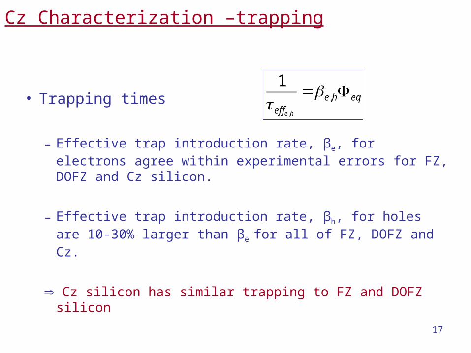
• Trapping times
– Effective trap introduction rate, βe, for electrons agree within experimental errors for FZ, DOFZ and Cz silicon.
– Effective trap introduction rate, βh, for holes are 10-30% larger than βe for all of FZ, DOFZ and Cz.
Cz silicon has similar trapping to FZ and DOFZ silicon
Cz Characterization –trapping
eqheeff he
,
,
1
18
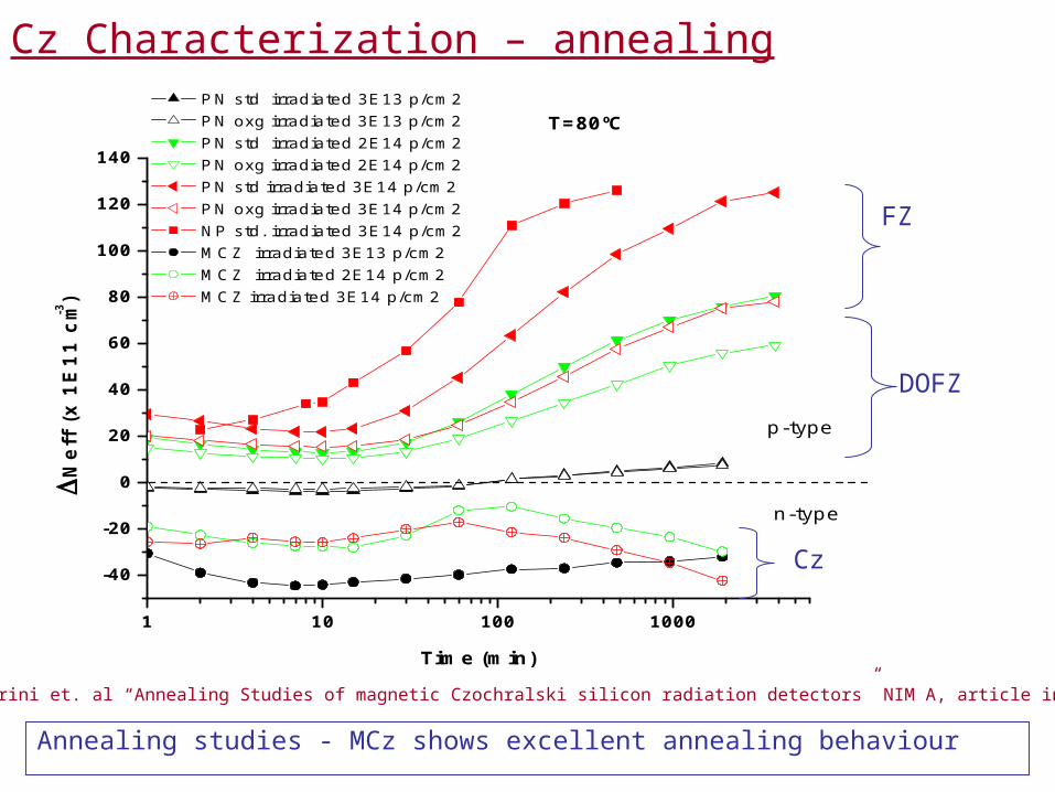
1 10 100 1000
-40
-20
0
20
40
60
80
100
120
140
p-type
T=80ºC
N
eff
(x
1E
11
cm-3
)
Time (min)
PN std irradiated 3E13 p/cm2 PN oxg irradiated 3E13 p/cm2 PN std irradiated 2E14 p/cm2 PN oxg irradiated 2E14 p/cm2 PN std irradiated 3E14 p/cm2 PN oxg irradiated 3E14 p/cm2 NP std. irradiated 3E14 p/cm2 MCZ irradiated 3E13 p/cm2 MCZ irradiated 2E14 p/cm2 MCZ irradiated 3E14 p/cm2
n-type
Annealing studies - MCz shows excellent annealing behaviour
Cz Characterization – annealing
G. Pellegrini et. al “Annealing Studies of magnetic Czochralski silicon radiation detectors” NIM A, article in press
Cz
FZ
DOFZ

19
• Test beam at the CERN SPS of a MCz detector* before and after irradiation– LHC speed electronics (40MHz)
(3 SCTA (analogue) chips)
– p+-on-n MCz material– Area read out = 6.1 x 1.92 cm– 380 m thick– 1150 cm (after processing)– 50 m pitch parallel strips– Vdep measured = 420 V (CV)
*Many thanks to the Helsinki Institute of Physics for
the MCz detector
Cz Characterization – test beam
NIM A 535 (2004) 428

20
MCz test beam results
S / N > 23.5 + 2.5
(380 m thick)
Depleted the detector (~550 V)
(CV measured Vdep ~ 420 V)
• 1.3 x 10¹⁴ 24 GeV p/cm2 S/N = 15
• 4.3 x 10¹⁴ 24 GeV p/cm2 S/N = 11 (under depleted)
• 7.0 x 10¹⁴ 24 GeV p/cm2 S/N = 7
(under depleted)
Sig
nal
[A
DC
Co
un
ts]
Bias Voltage [V]]S
ign
al [
AD
C C
ou
nts
]Bias Voltage [V]]
Unirradiated Detector Irradiated Detector
21
• Czochralski silicon is a cheap and standard industrial method for growing high purity silicon.
• Cz silicon – shows increased radiation hardness when compared to FZ or
DOFZ with charged irradiation– does not type invert with charged particle radiation
(up to a 24 GeV/c proton fluence of 5.1014 p/cm2)
– has the same trapping behaviour as FZ and DOFZ– has small variation in Neff with annealing time
• Cz strip detector read out with LHC speed electronics shows promising results both before and after irradiation.
Cz Characterization – Conclusions
Is Czochralski silicon something to get excited about?
22
Back up slides

23
5 101 5 102 5 103
time [ min ]
20406080
100120140160180
Vfd
[V]
0.5
1.0
1.5
2.0
2.5
| Nef
f | [
1012
cm
-3 ]
DOFZ (d1) - Vfd from CVDOFZ (d1) - Vfd from IV
5 101 5 102 5 103
time [ min ]
50
100
150
200
Vfd
[V
]
0.5
1.0
1.5
2.0
2.5
| Nef
f | [
1012
cm
-3 ]
MCZ (n320) - Vfd from CVMCZ (n320) - Vfd from IV
The evolution of the depletion voltage as determined by CV and IV methods for MCz silicon.
The evolution of the depletion voltage as determined by CV and IV methods for DOFZ (d1) silicon

24
• IRST, CNM, CiS, HIP and BNL have successfully produced Cz detectors.
• Sumitomo is no longer accessible and Okmetric Oyj require large orders (>1000 wafers per order)
Cz Characterization – procurement

25
0 1x10¹⁴
2x10¹⁴
3x10¹⁴
4x10¹⁴
5x10¹⁴
6x10¹⁴
7x10¹⁴
8x10¹⁴
9x10¹⁴
1x10¹⁵
0
1x10¹²
2x10¹²
3x10¹²
4x10¹²
5x10¹²
6x10¹²
7x10¹²
8x10¹²
9x10¹²
0
100
200
300
400
500
Ne
ff(c
m-3
)
Proton fluence (cm-2)
PN std PN oxg MCZ N-N oxg. P-stop 1E13 N-P std P-stop 10E13
Fu
ll dep
letion
voltag
e (V)
Confirmation of MCz depletion voltage behaviour of MCz after 24 GeV/c proton irradiation by G. Pellegrini et. al “Annealing Studies of magnetic Czochralski silicon radiation detectors” NIM A, article in press.
MCz
FZ
DOFZSCSI?
SCSI
Cz Characterization – proton irradiation
26
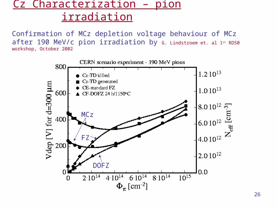
Confirmation of MCz depletion voltage behaviour of MCz after 190 MeV/c pion irradiation by G. Lindstroem et. al 1st RD50 workshop, October 2002
MCz
DOFZ
FZ
Cz Characterization – pion irradiation

27
0
100
200
300
400
500
600
700
0.0 0.2 0.4 0.6 0.8 1.0
Fluence (1015 1 MeV equivalent neutrons/cm2)
Vde
p (V
)
The minimum of Vdep is reached at 1-1.5×10¹⁴ n/cm2. Vdep is 650 at 1015 n/cm2.
Measurements after irradiation and before annealing
Cz Characterization – neutron irradiation

28
Cz Characterization – leakage current
5x5 mm2 p+n silicon diodes have been characterized before and after 24 GeV/c proton irradiation at the CERN PS.
Diodes processed at the Helsinki Institute of Physics from FZ, DOFZ and MCz silicon manufactured at Okmetric Oyj.
Crystal
orientation
ρ (kΩcm) Oxygenation Thickness (μm)
Initial
Vfd (V)
FZ <100> 1 - 295 ± 2 235 ± 15
DOFZ <100> 1 75h at 1100oC 295 ± 2 269 ± 7
MCz <100> 1 - 304 ± 2 309 ± 5
Diode0 2 4 6 8 10 12
De
ple
tion
Volt
ag
e [
V]
200
220
240
260
280
300
320
340
360
MCz (n320)
DOFZ (d1)
FZ (f2)
Depletion voltages for FZ, DOFZ and MCz diodes before irradiation
Single guard ring was always connected.

29
1013 5 1014 524 GeV/c protons [ cm-2 ]
50
100
150
200
250V
fd [V
]
1
2
3
| Nef
f | [
1012
cm
-3 ]
FZ (f2) - Vfd from CVFZ (f2) - Vfd from IV
Cz Characterization – proton irradiation
• Diodes measured after 24 GeV/c proton irradiation and 4mins/80oC annealing with IV and CV techniques. • Guard ring connected. • CV measurements made with 10kHz in parallel mode.
FZ silicon
SCSI

30
1013 5 1014 524 GeV/c protons [ cm-2 ]
50
100
150
200
250V
fd [V
]
1
2
3
| Nef
f | [
1012
cm
-3 ]
FZ (f2) - Vfd from CVFZ (f2) - Vfd from IV
• Diodes measured after 24 GeV/c proton irradiation and 4mins/80oC annealing with IV and CV techniques. • Guard ring connected. • CV measurements made with 10kHz in parallel mode.
MCz silicon
SCSI
1013 5 1014 524 GeV/c protons [ cm-2 ]
50
100
150
200
250
300V
fd [V
]
1
2
3
4
| Nef
f | [
1012
cm
-3 ]
MCZ (n320) - Vfd from IVMCZ (n320) - Vfd from CV
SCSI?
Cz Characterization – proton irradiation
31
TCT in MCz
14
Alison Bates
I [V
/50O
hms]
Low field
High field
Time [ns]
I [V
/50O
hms]
Low field
High field
14 Confirmed by Gregor Kramberger et. al
Hole injection signal
1013 5 1014 524 GeV/c protons [ cm-2 ]
50
100
150
200
250
300
Vfd
[V]
1
2
3
4
| Nef
f | [
1012
cm
-3 ]
MCZ (n320) - Vfd from IVMCZ (n320) - Vfd from CV
5x10¹⁴ p/cm2
NO TYPE INVERSION IN CZ SILICON UP TO 5x10¹⁴ p/cm2
• MCz silicon always has the high electric field on the structured side of the detector even after high fluences using standard p+-on-n MCz detectors

32
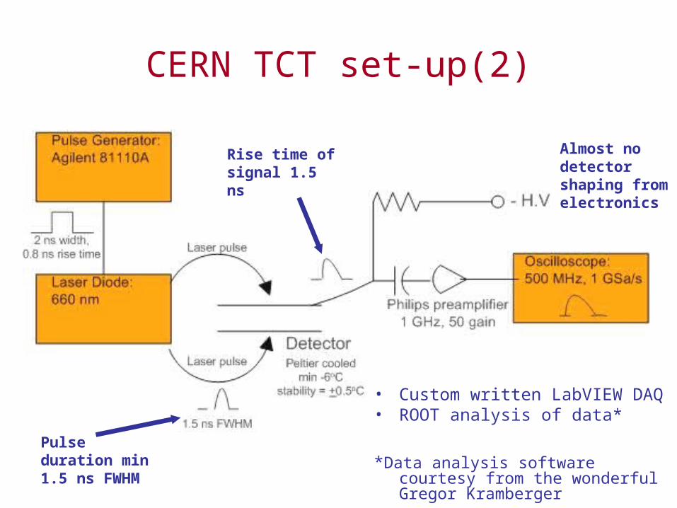
CERN TCT set-up(1)
• Easy detector mounting• Floating guard ring
• Front and back illumination possible
• Peltier cooled to ~-10oC• Temp. stability to +0.1oC• Flushed with N2 gas
• Red 660 nm laser diode• IR 1060 nm laser diode • Amount of charge deposited can be
tuned - laser diode output controlled by pulse generator signal
Cu/Be spring contact to front pad
Au PCB for ground plate
Laser fibre for illuminating the top of the detector
Water cooling and gas system
33
CERN TCT set-up(2)
Pulse duration min 1.5 ns FWHM
Rise time of signal 1.5 ns
Almost no detector shaping from electronics
• Custom written LabVIEW DAQ• ROOT analysis of data*
*Data analysis software courtesy from the wonderful Gregor Kramberger

34
Signal treatment
• Deconvolution of the true signal from the measured signal
Measured signal = detector signal transfer function
Transfer function:
I(t)=TCT/R x dUosc(t)/dt + Uosc(t)/R
R = 50 from input of preamp
TCT= RCd (Cd = detector capacitance)
Time [ns]
I [V
/50
]
35
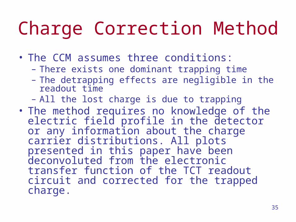
Charge Correction Method
• The CCM assumes three conditions:– There exists one dominant trapping time– The detrapping effects are negligible in the readout
time– All the lost charge is due to trapping
• The method requires no knowledge of the electric field profile in the detector or any information about the charge carrier distributions. All plots presented in this paper have been deconvoluted from the electronic transfer function of the TCT readout circuit and corrected for the trapped charge.

36
parameter summary
e h
[10-16 cm2/ns] [10-16 cm2/ns]
FZ (f2) 5.59 + 0.29 7.16 + 0.32
DOFZ (d1) 5.73 + 0.29 6.88 + 0.34
MCz (n320) 5.81 + 0.32 7.78 + 0.39
DOFZ (W317) 5.48 + 0.22 6.02 + 0.29
Dortmund [2]DOFZ
5.08 + 0.16 4.90 + 0.16
Ljubljana [3]DOFZ and FZ
5.34 + 0.19 7.08 + 0.18
Lancaster/Hamburg [4] FZ 5.32 + 0.30 6.81 + 0.29
Hamburg [5]FZ, DOFZ and Cz
5.07 + 0.16 6.20 + 0.54
Table 4. Comparison of βe and βh determined after 24 GeV/c proton irradiation. The top 4 rows are the values found in this work while the last four rows show data previously obtained by other groups. All values
have been scaled to 5oC, for the temperature dependence of β (see section 4.5).
37
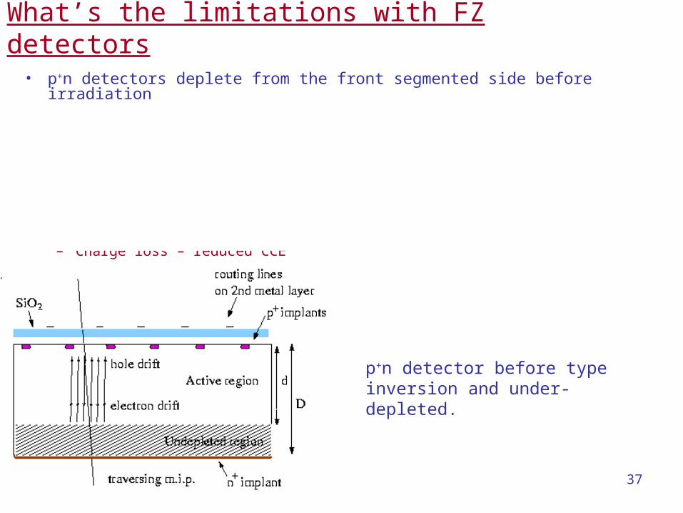
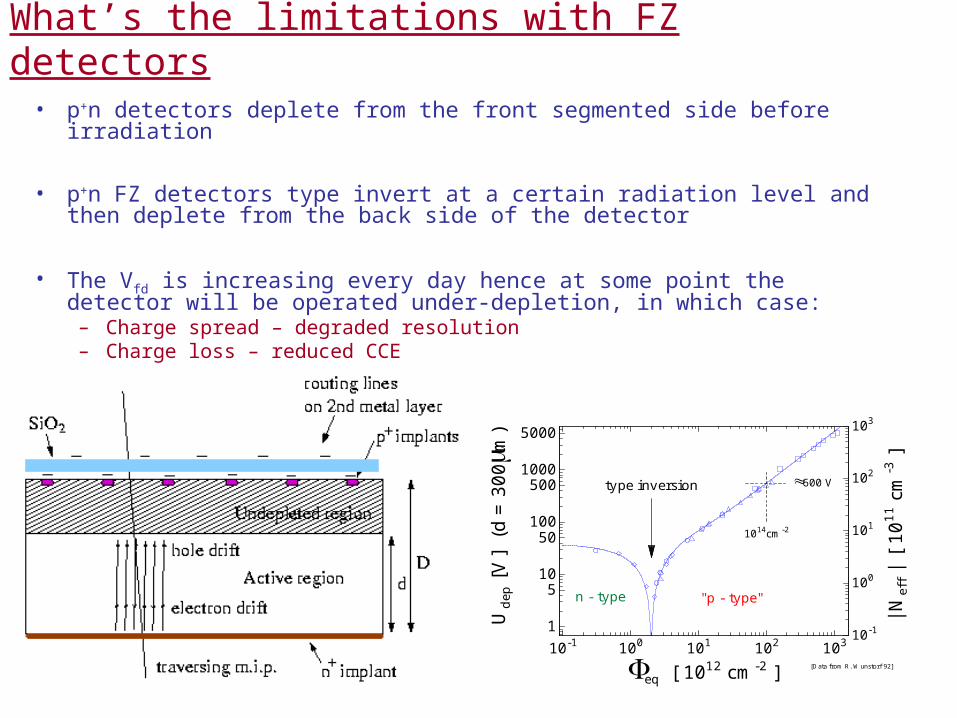
What’s the limitations with FZ detectors
• p+n detectors deplete from the front segmented side before irradiation
• p+n FZ detectors type invert at a certain radiation level and then deplete from the back side of the detector
• The Vfd is increasing every day hence at some point the detector will be operated under-depletion, in which case:
– Charge spread – degraded resolution– Charge loss – reduced CCE
p+n detector before type inversion and under-depleted.
38
What’s the limitations with FZ detectors
• p+n detectors deplete from the front segmented side before irradiation
• p+n FZ detectors type invert at a certain radiation level and then deplete from the back side of the detector
• The Vfd is increasing every day hence at some point the detector will be operated under-depletion, in which case:
– Charge spread – degraded resolution– Charge loss – reduced CCE
10-1 100 101 102 103
eq [ 1012 cm-2 ]
1
510
50100
5001000
5000
Ude
p [V
] (d
= 3
00m
)
10-1
100
101
102
103
| Nef
f | [
1011
cm
-3 ]
600 V 600 V
1014cm-21014cm-2
"p - type""p - type"
type inversiontype inversion
n - typen - type
[Data from R. Wunstorf 92]

39
n-on-n silicon, under-depleted:
•Limited loss in CCE
•Less degradation with under-depletion
Depletion fraction
reso
luti
on
n+on-n
Charge spread for p+on-n Si
For LHCb n+on-n detectors are the technology choice
40
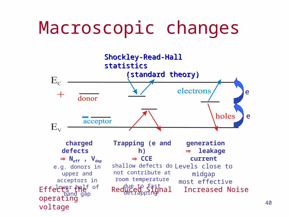
Macroscopic changes
Shockley-Read-Hall statistics Shockley-Read-Hall statistics (standard theory) (standard theory)
Trapping (e and h) CCE
shallow defects do not contribute at room
temperature due to fast detrapping
charged defects
Neff , Vdep
e.g. donors in upper and acceptors in lower half of band
gap
generation leakage current
Levels close to midgap
most effective
Increased NoiseReduced SignalEffects the operating voltage
e
e

41
Depletion voltage in FZ silicon
• Neff – Effective doping concentration
• Neff positive – n-type silicon (e.g. Phosphorus doped – donor)
• Neff negative – p-type silicon (e.g. Boron doped – acceptor)
• Donor removal and acceptor generation
– type inversion: n p– depletion width grows from n+
contact
2d
VN dep
eff
10-1 100 101 102 103
eq [ 1012 cm-2 ]
1
510
50100
5001000
5000
Ude
p [V
] (d
= 3
00m
)
10-1
100
101
102
103
| Nef
f | [
1011
cm
-3 ]
600 V 600 V
1014cm-21014cm-2
"p - type""p - type"
type inversiontype inversion
n - typen - type
[Data from R. Wunstorf 92]
cNN effeff exp0Neff(0) is the effective doping concentration before irradiation = 0.025cm-1 measured after beneficial anneal
before inversion
after inversion
n+ p+ n+
42
• Defects located close to the middle of the bandgap can generate current.
• Damage parameter (slope)
independent of eq and impurities
used for fluence calibration
Reverse current and Carrier Trapping
eqV
I
.
1011 1012 1013 1014 1015
eq [cm-2]
10-6
10-5
10-4
10-3
10-2
10-1
I /
V
[A/c
m3 ]
n-type FZ - 7 to 25 Kcmn-type FZ - 7 to 25 Kcmn-type FZ - 7 Kcmn-type FZ - 7 Kcmn-type FZ - 4 Kcmn-type FZ - 4 Kcmn-type FZ - 3 Kcmn-type FZ - 3 Kcm
n-type FZ - 780 cmn-type FZ - 780 cmn-type FZ - 410 cmn-type FZ - 410 cmn-type FZ - 130 cmn-type FZ - 130 cmn-type FZ - 110 cmn-type FZ - 110 cmn-type CZ - 140 cmn-type CZ - 140 cm
p-type EPI - 2 and 4 Kcmp-type EPI - 2 and 4 Kcm
p-type EPI - 380 cmp-type EPI - 380 cm
kT
ETTI g
2exp2
T dependence
• Defects can trap the charge carriers
• CCE = Charge Collection Efficiency
• CCE is reduced by radiation induced traps
• Problems arise if the de-trapping time becomes less than 25ns for the LHC
• t is the carrier transient time (e or h), β is a constant.
eqtrapping
tt
CCE
exp)exp(
Material independent