Arria V SoC開発ボード リファレンス・マニュアル...2014年7月 Altera Corporation Arria V SoC開発ボード リファレンス・マニュアル 1. この資料について

101 Innovation DriveSan Jose, CA 95134www.altera.com
MNL-01077-2.3
Reference Manual
Cyclone V SoC Development Board
Feedback Subscribe
Cyclone V SoC Development Board Reference Manual

© 2015 Altera Corporation. All rights reserved. ALTERA, ARRIA, CYCLONE, HARDCOPY, MAX, MEGACORE, NIOS, QUARTUS and STRATIX words and logosare trademarks of Altera Corporation and registered in the U.S. Patent and Trademark Office and in other countries. All other words and logos identified astrademarks or service marks are the property of their respective holders as described at www.altera.com/common/legal.html. Altera warrants performance of itssemiconductor products to current specifications in accordance with Altera's standard warranty, but reserves the right to make changes to any products andservices at any time without notice. Altera assumes no responsibility or liability arising out of the application or use of any information, product, or servicedescribed herein except as expressly agreed to in writing by Altera. Altera customers are advised to obtain the latest version of device specifications before relyingon any published information and before placing orders for products or services.
September 2015 Altera Corporation Cyclone V SoC Development BoardReference Manual
ISO 9001:2008 Registered
September 2015 Altera Corporation
Contents
Chapter 1. OverviewGeneral Description . . . . . . . . . . . . . . . . . . . . . . . . . . . . . . . . . . . . . . . . . . . . . . . . . . . . . . . . . . . . . . . . . . . . . 1–1Board Component Blocks . . . . . . . . . . . . . . . . . . . . . . . . . . . . . . . . . . . . . . . . . . . . . . . . . . . . . . . . . . . . . . . . . 1–2Development Board Block Diagram . . . . . . . . . . . . . . . . . . . . . . . . . . . . . . . . . . . . . . . . . . . . . . . . . . . . . . . . 1–4Handling the Board . . . . . . . . . . . . . . . . . . . . . . . . . . . . . . . . . . . . . . . . . . . . . . . . . . . . . . . . . . . . . . . . . . . . . . 1–4
Chapter 2. Board ComponentsBoard Overview . . . . . . . . . . . . . . . . . . . . . . . . . . . . . . . . . . . . . . . . . . . . . . . . . . . . . . . . . . . . . . . . . . . . . . . . . 2–2Featured Device: Cyclone V SoC . . . . . . . . . . . . . . . . . . . . . . . . . . . . . . . . . . . . . . . . . . . . . . . . . . . . . . . . . . . 2–5
I/O Resources . . . . . . . . . . . . . . . . . . . . . . . . . . . . . . . . . . . . . . . . . . . . . . . . . . . . . . . . . . . . . . . . . . . . . . . . 2–5MAX V CPLD 5M2210 System Controller . . . . . . . . . . . . . . . . . . . . . . . . . . . . . . . . . . . . . . . . . . . . . . . . . . . 2–6FPGA Configuration . . . . . . . . . . . . . . . . . . . . . . . . . . . . . . . . . . . . . . . . . . . . . . . . . . . . . . . . . . . . . . . . . . . . 2–11
FPGA Programming over Embedded USB-Blaster II . . . . . . . . . . . . . . . . . . . . . . . . . . . . . . . . . . . . . . 2–11FPGA Programming from Flash Memory . . . . . . . . . . . . . . . . . . . . . . . . . . . . . . . . . . . . . . . . . . . . . . . 2–14FPGA Programming over External USB-Blaster . . . . . . . . . . . . . . . . . . . . . . . . . . . . . . . . . . . . . . . . . . 2–15FPGA Programming using EPCQ . . . . . . . . . . . . . . . . . . . . . . . . . . . . . . . . . . . . . . . . . . . . . . . . . . . . . . 2–16
Status Elements . . . . . . . . . . . . . . . . . . . . . . . . . . . . . . . . . . . . . . . . . . . . . . . . . . . . . . . . . . . . . . . . . . . . . . . . 2–16Setup Elements . . . . . . . . . . . . . . . . . . . . . . . . . . . . . . . . . . . . . . . . . . . . . . . . . . . . . . . . . . . . . . . . . . . . . . . . 2–17
Board Settings DIP Switch . . . . . . . . . . . . . . . . . . . . . . . . . . . . . . . . . . . . . . . . . . . . . . . . . . . . . . . . . . . . . 2–17JTAG Chain Control DIP Switch . . . . . . . . . . . . . . . . . . . . . . . . . . . . . . . . . . . . . . . . . . . . . . . . . . . . . . . 2–18FPGA Configuration Mode DIP Switch . . . . . . . . . . . . . . . . . . . . . . . . . . . . . . . . . . . . . . . . . . . . . . . . . 2–18HPS Jumpers . . . . . . . . . . . . . . . . . . . . . . . . . . . . . . . . . . . . . . . . . . . . . . . . . . . . . . . . . . . . . . . . . . . . . . . . 2–19CPU Reset Push Button . . . . . . . . . . . . . . . . . . . . . . . . . . . . . . . . . . . . . . . . . . . . . . . . . . . . . . . . . . . . . . . 2–19MAX V Reset Push Button . . . . . . . . . . . . . . . . . . . . . . . . . . . . . . . . . . . . . . . . . . . . . . . . . . . . . . . . . . . . 2–20Program Configuration Push Button . . . . . . . . . . . . . . . . . . . . . . . . . . . . . . . . . . . . . . . . . . . . . . . . . . . . 2–20Program Select Push Button . . . . . . . . . . . . . . . . . . . . . . . . . . . . . . . . . . . . . . . . . . . . . . . . . . . . . . . . . . . 2–20Mictor Jumper . . . . . . . . . . . . . . . . . . . . . . . . . . . . . . . . . . . . . . . . . . . . . . . . . . . . . . . . . . . . . . . . . . . . . . . 2–20
General User Input/Output . . . . . . . . . . . . . . . . . . . . . . . . . . . . . . . . . . . . . . . . . . . . . . . . . . . . . . . . . . . . . 2–20User-Defined Push Buttons . . . . . . . . . . . . . . . . . . . . . . . . . . . . . . . . . . . . . . . . . . . . . . . . . . . . . . . . . . . . 2–20User-Defined DIP Switch . . . . . . . . . . . . . . . . . . . . . . . . . . . . . . . . . . . . . . . . . . . . . . . . . . . . . . . . . . . . . 2–22User-Defined LEDs . . . . . . . . . . . . . . . . . . . . . . . . . . . . . . . . . . . . . . . . . . . . . . . . . . . . . . . . . . . . . . . . . . . 2–22Expansion Header . . . . . . . . . . . . . . . . . . . . . . . . . . . . . . . . . . . . . . . . . . . . . . . . . . . . . . . . . . . . . . . . . . . 2–23Character LCD . . . . . . . . . . . . . . . . . . . . . . . . . . . . . . . . . . . . . . . . . . . . . . . . . . . . . . . . . . . . . . . . . . . . . . 2–23
Clock Circuitry . . . . . . . . . . . . . . . . . . . . . . . . . . . . . . . . . . . . . . . . . . . . . . . . . . . . . . . . . . . . . . . . . . . . . . . . . 2–24On-Board Oscillators . . . . . . . . . . . . . . . . . . . . . . . . . . . . . . . . . . . . . . . . . . . . . . . . . . . . . . . . . . . . . . . . . 2–24Off-Board Input/Output Clock . . . . . . . . . . . . . . . . . . . . . . . . . . . . . . . . . . . . . . . . . . . . . . . . . . . . . . . . 2–25
Components and Interfaces . . . . . . . . . . . . . . . . . . . . . . . . . . . . . . . . . . . . . . . . . . . . . . . . . . . . . . . . . . . . . . 2–26PCI Express . . . . . . . . . . . . . . . . . . . . . . . . . . . . . . . . . . . . . . . . . . . . . . . . . . . . . . . . . . . . . . . . . . . . . . . . . 2–2610/100/1000 Ethernet (HPS) . . . . . . . . . . . . . . . . . . . . . . . . . . . . . . . . . . . . . . . . . . . . . . . . . . . . . . . . . . . 2–2810/100 Ethernet (FPGA) . . . . . . . . . . . . . . . . . . . . . . . . . . . . . . . . . . . . . . . . . . . . . . . . . . . . . . . . . . . . . . 2–30HSMC . . . . . . . . . . . . . . . . . . . . . . . . . . . . . . . . . . . . . . . . . . . . . . . . . . . . . . . . . . . . . . . . . . . . . . . . . . . . . . 2–32RS-232 UART (HPS) . . . . . . . . . . . . . . . . . . . . . . . . . . . . . . . . . . . . . . . . . . . . . . . . . . . . . . . . . . . . . . . . . . 2–36CAN Bus (HPS) . . . . . . . . . . . . . . . . . . . . . . . . . . . . . . . . . . . . . . . . . . . . . . . . . . . . . . . . . . . . . . . . . . . . . . 2–36Real-Time Clock (HPS) . . . . . . . . . . . . . . . . . . . . . . . . . . . . . . . . . . . . . . . . . . . . . . . . . . . . . . . . . . . . . . . 2–37SPI Master . . . . . . . . . . . . . . . . . . . . . . . . . . . . . . . . . . . . . . . . . . . . . . . . . . . . . . . . . . . . . . . . . . . . . . . . . . 2–37I2C Interface . . . . . . . . . . . . . . . . . . . . . . . . . . . . . . . . . . . . . . . . . . . . . . . . . . . . . . . . . . . . . . . . . . . . . . . . . 2–38SDI Video . . . . . . . . . . . . . . . . . . . . . . . . . . . . . . . . . . . . . . . . . . . . . . . . . . . . . . . . . . . . . . . . . . . . . . . . . . . 2–38
SDI Video Output . . . . . . . . . . . . . . . . . . . . . . . . . . . . . . . . . . . . . . . . . . . . . . . . . . . . . . . . . . . . . . . . . 2–38
Cyclone V SoC Development BoardReference Manual
iv Contents
SDI Video Input . . . . . . . . . . . . . . . . . . . . . . . . . . . . . . . . . . . . . . . . . . . . . . . . . . . . . . . . . . . . . . . . . . . 2–39Memory . . . . . . . . . . . . . . . . . . . . . . . . . . . . . . . . . . . . . . . . . . . . . . . . . . . . . . . . . . . . . . . . . . . . . . . . . . . . . . . 2–40
DDR3 SDRAM (FPGA) . . . . . . . . . . . . . . . . . . . . . . . . . . . . . . . . . . . . . . . . . . . . . . . . . . . . . . . . . . . . . . . 2–40DDR3 SDRAM (HPS) . . . . . . . . . . . . . . . . . . . . . . . . . . . . . . . . . . . . . . . . . . . . . . . . . . . . . . . . . . . . . . . . . 2–43QSPI Flash (HPS) . . . . . . . . . . . . . . . . . . . . . . . . . . . . . . . . . . . . . . . . . . . . . . . . . . . . . . . . . . . . . . . . . . . . 2–48EPCQ Flash . . . . . . . . . . . . . . . . . . . . . . . . . . . . . . . . . . . . . . . . . . . . . . . . . . . . . . . . . . . . . . . . . . . . . . . . . 2–48CFI Flash . . . . . . . . . . . . . . . . . . . . . . . . . . . . . . . . . . . . . . . . . . . . . . . . . . . . . . . . . . . . . . . . . . . . . . . . . . . 2–49Micro SD Flash Memory . . . . . . . . . . . . . . . . . . . . . . . . . . . . . . . . . . . . . . . . . . . . . . . . . . . . . . . . . . . . . . 2–50I2C EEPROM . . . . . . . . . . . . . . . . . . . . . . . . . . . . . . . . . . . . . . . . . . . . . . . . . . . . . . . . . . . . . . . . . . . . . . . . 2–51
Power Supply . . . . . . . . . . . . . . . . . . . . . . . . . . . . . . . . . . . . . . . . . . . . . . . . . . . . . . . . . . . . . . . . . . . . . . . . . . 2–51Power Distribution System . . . . . . . . . . . . . . . . . . . . . . . . . . . . . . . . . . . . . . . . . . . . . . . . . . . . . . . . . . . . 2–52Power Measurement . . . . . . . . . . . . . . . . . . . . . . . . . . . . . . . . . . . . . . . . . . . . . . . . . . . . . . . . . . . . . . . . . 2–54
Chapter 3. Board Components ReferenceStatement of China-RoHS Compliance . . . . . . . . . . . . . . . . . . . . . . . . . . . . . . . . . . . . . . . . . . . . . . . . . . . . . 3–3CE EMI Conformity Caution . . . . . . . . . . . . . . . . . . . . . . . . . . . . . . . . . . . . . . . . . . . . . . . . . . . . . . . . . . . . . . 3–3
Additional InformationBoard Revision History . . . . . . . . . . . . . . . . . . . . . . . . . . . . . . . . . . . . . . . . . . . . . . . . . . . . . . . . . . . . . . . Info–1Document Revision History . . . . . . . . . . . . . . . . . . . . . . . . . . . . . . . . . . . . . . . . . . . . . . . . . . . . . . . . . . . Info–1How to Contact Altera . . . . . . . . . . . . . . . . . . . . . . . . . . . . . . . . . . . . . . . . . . . . . . . . . . . . . . . . . . . . . . . . Info–2Typographic Conventions . . . . . . . . . . . . . . . . . . . . . . . . . . . . . . . . . . . . . . . . . . . . . . . . . . . . . . . . . . . . . Info–2
Cyclone V SoC Development Board September 2015 Altera CorporationReference Manual
September 2015 Altera Corporation
1. Overview
This document describes the hardware features of the Cyclone® V SoC development board, including the detailed pin-out and component reference information required to create custom FPGA designs that interface with all components of the board.
General DescriptionThe Cyclone V SoC development board provides a hardware platform for developing and prototyping low-power, high-performance, and logic-intensive designs using Altera’s Cyclone V SoC. The board provides a wide range of peripherals and memory interfaces to facilitate the development of Cyclone V SoC designs.
One high-speed mezzanine card (HSMC) connector is available to add additional functionality via a variety of HSMCs available from Altera® and various partners.
f For more information on the following topics, refer to the respective documents:
■ Cyclone V device family, refer to the Cyclone V Device Handbook.
■ HSMC Specification, refer to the High Speed Mezzanine Card (HSMC) Specification.
■ A list of the latest HSMCs available, refer to the Development Board Daughtercards page of the Altera website.
Cyclone V SoC Development BoardReference Manual
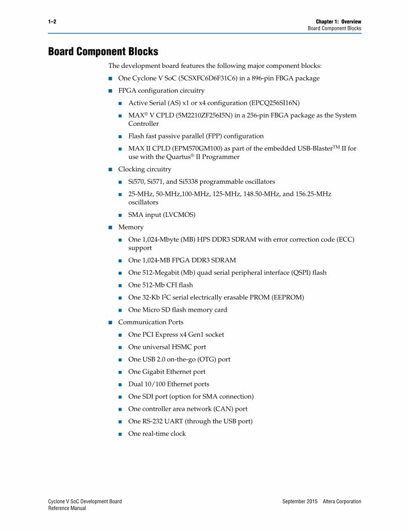
1–2 Chapter 1: OverviewBoard Component Blocks
Board Component BlocksThe development board features the following major component blocks:
■ One Cyclone V SoC (5CSXFC6D6F31C6) in a 896-pin FBGA package
■ FPGA configuration circuitry
■ Active Serial (AS) x1 or x4 configuration (EPCQ256SI16N)
■ MAX® V CPLD (5M2210ZF256I5N) in a 256-pin FBGA package as the System Controller
■ Flash fast passive parallel (FPP) configuration
■ MAX II CPLD (EPM570GM100) as part of the embedded USB-BlasterTM II for use with the Quartus® II Programmer
■ Clocking circuitry
■ Si570, Si571, and Si5338 programmable oscillators
■ 25-MHz, 50-MHz,100-MHz, 125-MHz, 148.50-MHz, and 156.25-MHz oscillators
■ SMA input (LVCMOS)
■ Memory
■ One 1,024-Mbyte (MB) HPS DDR3 SDRAM with error correction code (ECC) support
■ One 1,024-MB FPGA DDR3 SDRAM
■ One 512-Megabit (Mb) quad serial peripheral interface (QSPI) flash
■ One 512-Mb CFI flash
■ One 32-Kb I2C serial electrically erasable PROM (EEPROM)
■ One Micro SD flash memory card
■ Communication Ports
■ One PCI Express x4 Gen1 socket
■ One universal HSMC port
■ One USB 2.0 on-the-go (OTG) port
■ One Gigabit Ethernet port
■ Dual 10/100 Ethernet ports
■ One SDI port (option for SMA connection)
■ One controller area network (CAN) port
■ One RS-232 UART (through the USB port)
■ One real-time clock
Cyclone V SoC Development Board September 2015 Altera CorporationReference Manual

Chapter 1: Overview 1–3Board Component Blocks
■ General user input/output
■ LEDs and displays
■ Eight user LEDs
■ One configuration load LED
■ One configuration done LED
■ One error LED
■ Three configuration select LEDs
■ Four on-board USB-Blaster II status LEDs
■ One HSMC interface LED
■ Two UART data transmit and receive LEDs
■ One power on LED
■ One two-line character LCD display
■ Push buttons
■ One CPU reset push button
■ One MAX V reset push button
■ One program select push button
■ One program configuration push button
■ Six general user push buttons
■ DIP switches
■ One MAX V CPLD System Controller control switch
■ One JTAG chain control DIP switch
■ One mode select DIP switch
■ One general user DIP switch
■ Power supply
■ 14–20-V (laptop) DC input
■ Mechanical
■ 5.2" × 8.2" rectangular form factor
September 2015 Altera Corporation Cyclone V SoC Development BoardReference Manual

1–4 Chapter 1: OverviewDevelopment Board Block Diagram
Development Board Block DiagramFigure 1–1 shows a block diagram of the Cyclone V SoC development board.
Handling the BoardWhen handling the board, it is important to observe the following static discharge precaution:
c Without proper anti-static handling, the board can be damaged. Therefore, use anti-static handling precautions when touching the board.
Figure 1–1. Cyclone V SoC Development Board Block Diagram
JTAG Chain
LEDsDIP
SwitchesPush
Buttons
LVDS/Single-Ended
x4
x40
x40
x40
x4
x4
x4
x16
ADDR
XCVR
x4
XCVR
x4
XCVR
x4
x40
x8
CLK
IN x
3
CLK
OU
T x3
x8 C
ON
FIG
x4
x4
I2C
x1
x1
x1
x1
x8
x4 x4 x8 x1 x1
x19 BlasterAccelerator Bus
USB 2.0OTG
UART CAN
LCD Character
64-MB QSPIFlash
SD CardSocket
SPI + I2C LTCExp Header
EEPROM
Real-TimeClock
LTC Power I2CHeader
LTC PowerMonitor
1024 MBDDR3
1024 MBDDR3 + ECC
Push Buttons +DIP Switches
50 MHz /100 MHzFixed Oscillator
10/100Ethernet
10/100EtherCAT
REFCLKVCXO
LEDs
EPM570GM100Embedded
USB-Blaster IIand USB Interface
USB2.0
128-MBNORFlash
SDIx1
SMA
5M2210ZF256I5NSystem Controller
x4
GigabitEthernet PHY
5CSXFC6D6F31C7
FPGA
HPS
Cyclone V SoC Development Board September 2015 Altera CorporationReference Manual

September 2015 Altera Corporation
2. Board Components
This chapter introduces the major components on the Cyclone V SoC development board. Figure 2–1 illustrates the component locations and Table 2–1 provides a brief description of all component features of the board.
1 A complete set of schematics, a physical layout database, and fabrication files for the development board reside in the Cyclone V SoC development kit board design files directory.
f For information about powering up the board and installing the demonstration software, refer to the Cyclone V SoC Development Kit User Guide
This chapter consists of the following sections:
■ “Board Overview”
■ “Featured Device: Cyclone V SoC” on page 2–5
■ “MAX V CPLD 5M2210 System Controller” on page 2–6
■ “FPGA Configuration” on page 2–11
■ “General User Input/Output” on page 2–20
■ “Clock Circuitry” on page 2–24
■ “Components and Interfaces” on page 2–26
■ “Memory” on page 2–40
■ “Power Supply” on page 2–51
Cyclone V SoC Development BoardReference Manual

2–2 Chapter 2: Board ComponentsBoard Overview
Board OverviewThis section provides an overview of the Cyclone V SoC development board, including an annotated board image and component descriptions. Figure 2–1 shows an overview of the board features.
Table 2–1 describes the components and lists their corresponding board references.
Figure 2–1. Overview of the Cyclone V SoC Development Board Features
Table 2–1. Board Components (Part 1 of 3)
Board Reference Type Description
Featured Devices
U21 FPGA Cyclone V SoC, 5CSXFC6D6F31C6, 896-pin FBGA.
U19 CPLD MAX V CPLD, 5M2210ZF256I5N, 256-pin FBGA.
Configuration, Status, and Setup Elements
J23 JTAG chain header Provides access to the JTAG chain and disables the embedded USB-Blaster II when using an external USB-Blaster cable.
SW4 JTAG chain control DIP switch Remove or include devices in the active JTAG chain.
J37 USB header USB interface for FPGA programming and debugging through the embedded USB-Blaster II JTAG via a type-B USB cable.
SW2 Board settings DIP switchControls the MAX V CPLD 5M2210 System Controller functions such as clock enable, SMA clock input control, and which image to load from flash memory at power-up.
Cyclone V SoC Development Board September 2015 Altera CorporationReference Manual
Chapter 2: Board Components 2–3Board Overview
SW3 MSEL DIP switch Controls the configuration scheme on the board. MSEL pins 0, 1, 2 and 4 connects to the DIP switch while MSEL pin 3 connects to ground.
S11 Program select push button Toggles the program select LEDs, which selects the program image that loads from flash memory to the FPGA.
S12 Configure push button Load image from flash memory to the FPGA based on the settings of the program select LEDs.
D37 Configuration done LED Illuminates when the FPGA is configured.
D34 Load LED Illuminates when the MAX V CPLD 5M2210 System Controller is actively configuring the FPGA.
D36 Error LED Illuminates when the FPGA configuration from flash memory fails.
D35 Power LED Illuminates when 5.0-V power is present.
D30, D31 JTAG TX/RX LEDsIndicate the transmit or receive activity of the JTAG chain. The TX and RX LEDs would flicker if the link is in use and active. The LEDs are either off when not in use or on when in use but idle.
D39–D41 Program select LEDsIlluminates to show which flash memory image loads to the FPGA when you press the program select push button. Refer to Table 2–6 for the LED settings.
D9 HSMC port present LED Illuminates when a daughter card is plugged into the HSMC port.
D14, D15 UART LEDs Illuminates when UART transmitter and receiver are in use.
Clock Circuitry
X1 Programmable oscillatorProgrammable oscillator with a default frequency of 100 MHz. The frequency is programmable using the clock control GUI running on the MAX V CPLD 5M2210 System Controller.
X4 50-MHz oscillator 50.000-MHz crystal oscillator for general purpose logic.
X3 148.5-MHz oscillator
Programmable voltage-controlled crystal oscillator (VCXO) with a default frequency of 148.5 MHz. The frequency is programmable using the clock control GUI running on the MAX V CPLD 5M2210 System Controller.
J36 Clock input SMA connector Drive CMOS-compatible clock inputs into the clock multiplexer buffer.
U29 Multi-output oscillator Si5338C quad-output programmable oscillator with 100M, 25M, 25M, and 156.25M outputs.
U35 Multi-output oscillator Si5338C quad-output fixed oscillator with 25M, 25M, 100M, and 100M outputs.
General User Input/Output
D1–D8 User LEDs Eight user LEDs. Illuminates when driven low.
SW1 User DIP switch User DIP switch. When the switch is ON, a logic 0 is selected.
S10 CPU reset push button Reset the FPGA logic.
S2 MAX V reset push button Reset the MAX V CPLD 5M2210 System Controller.
S1–S6 General user push buttons Six user push buttons. Driven low when pressed.
Memory Devices
U37, U38, U30, U22, U14 DDR3 memory Two 4-Gb DDR3 SDRAM with a 16-bit data bus for the FPGA and three
4-Gb DDR3 SDRAM with a 16-bit data bus for the HPS.
U5 QSPI flash 1-Gb serial NOR flash with 4-bit data bus.
Table 2–1. Board Components (Part 2 of 3)
Board Reference Type Description
September 2015 Altera Corporation Cyclone V SoC Development BoardReference Manual

2–4 Chapter 2: Board ComponentsBoard Overview
U6 Flash memory 512-Mb synchronous flash devices with a 16-bit data bus for non-volatile memory.
U28 I2C EEPROM 32-Mb I2C serial EEPROM.
Communication Ports
J25 PCI Express socket PCI Express Gen1 ×4 socket.
J12 HSMC port Provides four transceiver channels and 84 CMOS or 17 LVDS channels per the HSMC specification.
J2 Gigabit Ethernet portRJ-45 connector which provides a 10/100/1000 Ethernet connection via a Micrel KSZ9021RN PHY and the FPGA-based Altera Triple Speed Ethernet MegaCore function in RGMII mode.
J33, J34 Gigabit Ethernet port RJ-45 connectors which provides a dual 10/100 Ethernet connection via a Renesas uPD60620A PHY in MII mode.
J35 CAN port DSUB 9-pin connector for CAN networking.
J8 USB-UART port USB connector with USB-to-UART bridge for RS-232 terminal.
J1 USB OTG port Micro-USB connector for OTG interface.
J3 Micro SD card socket Micro SD card interface with 4-bit data line.
J15, J16 Debug headers Two 2×8 headers for debug purposes.
Video and Display Ports
J15 Character LCD Connector that interfaces to a provided 16 character × 2 line LCD module along with two standoffs.
J14, J17 SDI video portTwo 75-Ω system management bus (SMB) connectors which provide a full-duplex SDI interface through a LMH0303 driver and LMH0384 cable equalizer.
Power Supply
J22 DC input jack Accepts 16-V DC power supply. Do not use this input jack while the board is plugged into a PCI Express slot.
SW5 Power switch Switch to power on or off the board when power is supplied from the DC input jack.
Table 2–1. Board Components (Part 3 of 3)
Board Reference Type Description
Cyclone V SoC Development Board September 2015 Altera CorporationReference Manual

Chapter 2: Board Components 2–5Featured Device: Cyclone V SoC
Featured Device: Cyclone V SoCThe Cyclone V SoC development board features a Cyclone V SoC 5CSXFC6D6F31C6 device (U21) that includes a hard processor system (HPS) with integrated ARM® Cortex™-A9 MPCore processor.
f For more information about Cyclone V device family, refer to the Cyclone V Device Handbook.
Table 2–2 describes the features of the Cyclone V SoC device.
I/O ResourcesThe Cyclone V SoC 5CSXFC6D6F31C6 device has 288 general purpose FPGA I/O pins and 181 general-purpose HPS I/O pins. Table 2–3 lists the Cyclone V SoC I/O pin count and usage by function on the board.
Table 2–2. Cyclone V SoC Features
Resource 5CSXFC6D6F31C6
LE (K) 110
ALM 41,509
Register 166,036
Memory (Kb)M10K 5,140
MLAB 621
18-bit × 18-bit Multiplier 224
PLLsFPGA 6
HPS 3
Transceivers (3 Gbps) 9
Table 2–3. Cyclone V SoC I/O Pin Count (Part 1 of 2)
Function I/O Standard I/O Count
HPS clock inputs 3.3-V LVCMOS 2
HPS resets 3.3-V LVCMOS 2
HPS LEDs 3.3-V LVCMOS 4
HPS buttons and switches 3.3-V LVCMOS 6
HPS UART 3.3-V LVCMOS 2
HPS I2C bus 3.3-V LVCMOS 2
HPS SPI bus 3.3-V LVCMOS 4
HPS QSPI flash 3.3-V LVCMOS 6
HPS SD card 3.3-V LVCMOS 7
HPS USB OTG 3.3-V LVCMOS 20
HPS Gigabit Ethernet 3.3-V LVCMOS 14
HPS CAN bus 3.3-V LVCMOS 2
HPS trace 3.3-V LVCMOS 9
HPS DDR3 1.5-V SSTL 78
September 2015 Altera Corporation Cyclone V SoC Development BoardReference Manual

2–6 Chapter 2: Board ComponentsMAX V CPLD 5M2210 System Controller
f For further information about I/O usage in the Cyclone V SoC packages, refer to "Package Plan" in the Cyclone V Device Overview.
MAX V CPLD 5M2210 System ControllerThe board utilizes the 5M2210ZF256I5N System Controller, an Altera MAX V CPLD, for the following purposes:
■ FPGA configuration from flash
■ Power measurement
■ Control and status registers (CSR) for remote system update
Figure 2–2 illustrates the MAX V CPLD 5M2210 System Controller's functionality and external circuit connections as a block diagram.
FPGA clock inputs mixed 5
FPGA LEDs 1.5-V 4
FPGA buttons and switches mixed 7
FPGA DDR3 1.5-V SSTL 71
FPGA Dual Ethernet 2.5-V 14
FPGA SDI control 2.5-V 8
FPGA SDI video 1.5-V PCML 4
FPGA MAX V SPI port 2.5-V 4
FPGA HSMC mixed 107
FPGA PCI Express control mixed 7
FPGA PCI Express transceivers 1.5-V PCML 4
Table 2–3. Cyclone V SoC I/O Pin Count (Part 2 of 2)
Function I/O Standard I/O Count
Figure 2–2. MAX V CPLD 5M2210 System Controller Block Diagram
Information Register
EmbeddedUSB-Blaster II
OscillatorController
SLD-HUB
PFL
SPI Bus
MAX V CPLD System Controller
LTC 2978Power
Controllers
Virtual-JTAG
PC
FPGA
I2CController
DecoderEncoder GPIO
JTAG Control
ControlRegister
Si570, Si571,Si5338
ProgrammableOscillator
Cyclone V SoC Development Board September 2015 Altera CorporationReference Manual

Chapter 2: Board Components 2–7MAX V CPLD 5M2210 System Controller
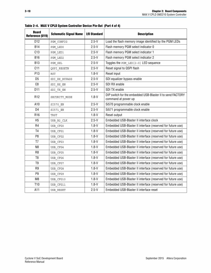
Table 2–4 lists the I/O signals present on the MAX V CPLD System Controller. The signal names and functions are relative to the MAX V device.
Table 2–4. MAX V CPLD System Controller Device Pin-Out (Part 1 of 4)
Board Reference (U19) Schematic Signal Name I/O Standard Description
B9 CLK125A_EN 2.5-V 125 MHz oscillator enable
E9 CLK50_EN 2.5-V 50 MHz oscillator enable
J5 CLK_100M_MAX 2.5-V 100 MHz clock input
J12 CLK_50M_MAX 1.8-V 50 MHz clock input
A13 CLK_SEL 2.5-V DIP switch for clock select—SMA or oscillator
D10 CPU_RESETN 2.5-V FPGA reset push button
T13 EXTRA_SIG1 1.8-V Embedded USB-Blaster II interface. Reserved for future use
T15 EXTRA_SIG2 1.8-V Embedded USB-Blaster II interface. Reserved for future use
A2 FACTORY_LOAD 2.5-V DIP switch to load factory or user design at power-up
R14 FACTORY_REQUEST 1.8-V Embedded USB-Blaster II request to send FACTORY command
N12 FACTORY_STATUS 1.8-V Embedded USB-Blaster II FACTORY command status
F11 FLASH_ADVN 1.8-V FSM bus flash memory address valid
N14 FLASH_CEN0 1.8-V FSM bus flash memory chip enable
D14 FLASH_CLK 1.8-V FSM bus flash memory clock
P15 FLASH_OEN 1.8-V FSM bus flash memory output enable
P14 FLASH_RDYBSYN 1.8-V FSM bus flash memory ready
D13 FLASH_RESETN 1.8-V FSM bus flash memory reset
N15 FLASH_WEN 1.8-V FSM bus flash memory write enable
E14 FM_A0 1.8-V FM address bus
C14 FM_A1 1.8-V FM address bus
C15 FM_A2 1.8-V FM address bus
E13 FM_A3 1.8-V FM address bus
E12 FM_A4 1.8-V FM address bus
D15 FM_A5 1.8-V FM address bus
F14 FM_A6 1.8-V FM address bus
D16 FM_A7 1.8-V FM address bus
F13 FM_A8 1.8-V FM address bus
E15 FM_A9 1.8-V FM address bus
E16 FM_A10 1.8-V FM address bus
F15 FM_A11 1.8-V FM address bus
G14 FM_A12 1.8-V FM address bus
F16 FM_A13 1.8-V FM address bus
G13 FM_A14 1.8-V FM address bus
G15 FM_A15 1.8-V FM address bus
G12 FM_A16 1.8-V FM address bus
G16 FM_A17 1.8-V FM address bus
September 2015 Altera Corporation Cyclone V SoC Development BoardReference Manual

2–8 Chapter 2: Board ComponentsMAX V CPLD 5M2210 System Controller
H14 FM_A18 1.8-V FM address bus
H15 FM_A19 1.8-V FM address bus
H13 FM_A20 1.8-V FM address bus
H16 FM_A21 1.8-V FM address bus
J13 FM_A22 1.8-V FM address bus
J16 FM_A23 1.8-V FM address bus
K12 FM_A24 1.8-V FM address bus
M14 FM_A25 1.8-V FM address bus
N13 FM_A26 1.8-V FM address bus
J14 FM_D0 1.8-V FM data bus
J15 FM_D1 1.8-V FM data bus
K16 FM_D2 1.8-V FM data bus
K13 FM_D3 1.8-V FM data bus
K15 FM_D4 1.8-V FM data bus
K14 FM_D5 1.8-V FM data bus
L16 FM_D6 1.8-V FM data bus
L11 FM_D7 1.8-V FM data bus
L15 FM_D8 1.8-V FM data bus
L12 FM_D9 1.8-V FM data bus
M16 FM_D10 1.8-V FM data bus
L13 FM_D11 1.8-V FM data bus
M15 FM_D12 1.8-V FM data bus
L14 FM_D13 1.8-V FM data bus
N16 FM_D14 1.8-V FM data bus
M13 FM_D15 1.8-V FM data bus
K1 FPGA_CONF_DONE 2.5-V FPGA configuration done LED
D3 FPGA_CONFIG_D0 2.5-V FPGA configuration data
C2 FPGA_CONFIG_D1 2.5-V FPGA configuration data
C3 FPGA_CONFIG_D2 2.5-V FPGA configuration data
E3 FPGA_CONFIG_D3 2.5-V FPGA configuration data
D2 FPGA_CONFIG_D4 2.5-V FPGA configuration data
E4 FPGA_CONFIG_D5 2.5-V FPGA configuration data
D1 FPGA_CONFIG_D6 2.5-V FPGA configuration data
E5 FPGA_CONFIG_D7 2.5-V FPGA configuration data
F3 FPGA_CONFIG_D8 2.5-V FPGA configuration data
E1 FPGA_CONFIG_D9 2.5-V FPGA configuration data
F4 FPGA_CONFIG_D10 2.5-V FPGA configuration data
F2 FPGA_CONFIG_D11 2.5-V FPGA configuration data
F1 FPGA_CONFIG_D12 2.5-V FPGA configuration data
Table 2–4. MAX V CPLD System Controller Device Pin-Out (Part 2 of 4)
Board Reference (U19) Schematic Signal Name I/O Standard Description
Cyclone V SoC Development Board September 2015 Altera CorporationReference Manual

Chapter 2: Board Components 2–9MAX V CPLD 5M2210 System Controller
F6 FPGA_CONFIG_D13 2.5-V FPGA configuration data
G2 FPGA_CONFIG_D14 2.5-V FPGA configuration data
G3 FPGA_CONFIG_D15 2.5-V FPGA configuration data
N3 FPGA_CVP_CONFDONE 2.5-V FPGA Configuration via Protocol (CvP) done
J3 FPGA_DCLK 2.5-V FPGA configuration clock
N1 FPGA_NCONFIG 2.5-V FPGA configuration active
J4 FPGA_NSTATUS 2.5-V FPGA configuration ready
H1 FPGA_PR_DONE 2.5-V FPGA partial reconfiguration done
P2 FPGA_PR_ERROR 2.5-V FPGA partial reconfiguration error
E2 FPGA_PR_READY 2.5-V FPGA partial reconfiguration ready
F5 FPGA_PR_REQUEST 2.5-V FPGA partial reconfiguration request
B11 HPS_RESETN 2.5-V HPS reset push button
B8 HSMA_PRSNTN 2.5-V HSMC port A present
M1 I2C_SCL_MAX 2.5-V Programmable oscillator I2C clock
M2 I2C_SDA_MAX 2.5-V Programmable oscillator I2C data
L6 JTAG_MAX_TDI 2.5-V JTAG chain data in
M5 JTAG_MAX_TDO 2.5-V JTAG chain data out
N4 JTAG_MAX_TMS 2.5-V JTAG chain mode
P3 JTAG_MUX_TCK 2.5-V JTAG chain clock
P11 M570_CLOCK 1.8-V 25-MHz clock to embedded USB-Blaster II for sending FACTORY command
L5 M570_PCIE_JTAG_EN 2.5-V M570 JTAG enable for the embedded USB-Blaster II
H2 MAX_AS_CONF 2.5-V Driven low to enable AS configuration from the EPCQ flash through U13 to the FPGA
E11 MAX_CONF_DONE 2.5-V Embedded USB-Blaster II configuration done LED
A4 MAX_ERROR 2.5-V FPGA configuration error LED
G4 MAX_FPGA_MISO 2.5-V FPGA to MAX V SPI bus data output
G1 MAX_FPGA_MOSI 2.5-V FPGA to MAX V SPI bus data input
H3 MAX_FPGA_SCK 2.5-V FPGA to MAX V SPI bus clock
G5 MAX_FPGA_SSEL 2.5-V FPGA to MAX V SPI bus slave select
A6 MAX_LOAD 2.5-V FPGA configuration active LED
M9 MAX_RESETN 2.5-V MAX V reset push button
B10 MSEL0 2.5-V FPGA MSEL0 setting
B3 MSEL1 2.5-V FPGA MSEL1 setting
C10 MSEL2 2.5-V FPGA MSEL2 setting
C12 MSEL3 2.5-V FPGA MSEL3 setting
C6 MSEL4 2.5-V FPGA MSEL4 setting
E10 OVERTEMP 2.5-V Temperature monitor fan enable
C7 PCIE_JTAG_EN 2.5-V PCIe JTAG master enable
Table 2–4. MAX V CPLD System Controller Device Pin-Out (Part 3 of 4)
Board Reference (U19) Schematic Signal Name I/O Standard Description
September 2015 Altera Corporation Cyclone V SoC Development BoardReference Manual
2–10 Chapter 2: Board ComponentsMAX V CPLD 5M2210 System Controller
D12 PGM_CONFIG 2.5-V Load the flash memory image identified by the PGM LEDs
B14 PGM_LED0 2.5-V Flash memory PGM select indicator 0
C13 PGM_LED1 2.5-V Flash memory PGM select indicator 1
B16 PGM_LED2 2.5-V Flash memory PGM select indicator 2
B13 PGM_SEL 2.5-V Toggles the PGM_LED[2:0] LED sequence
C11 QSPI_RESETN 2.5-V Reset signal to QSPI flash
P13 RST 1.8-V Reset input
D5 SDI_RX_BYPASS 2.5-V SDI equalizer bypass enable
E8 SDI_RX_EN 2.5-V SDI RX enable
D11 SDI_TX_EN 2.5-V SDI TX enable
R12 SECURITY_MODE 1.8-V DIP switch for the embedded USB-Blaster II to send FACTORY command at power up
A10 SI570_EN 2.5-V Si570 programmable clock enable
D4 SI571_EN 2.5-V Si571 programmable clock enable
R16 TRST 1.8-V Reset output
H5 USB_B2_CLK 2.5-V Embedded USB-Blaster II interface clock
R4 USB_CFG0 1.8-V Embedded USB-Blaster II interface (reserved for future use)
T4 USB_CFG1 1.8-V Embedded USB-Blaster II interface (reserved for future use)
P8 USB_CFG2 1.8-V Embedded USB-Blaster II interface (reserved for future use)
T7 USB_CFG3 1.8-V Embedded USB-Blaster II interface (reserved for future use)
N8 USB_CFG4 1.8-V Embedded USB-Blaster II interface (reserved for future use)
R8 USB_CFG5 1.8-V Embedded USB-Blaster II interface (reserved for future use)
T8 USB_CFG6 1.8-V Embedded USB-Blaster II interface (reserved for future use)
T9 USB_CFG7 1.8-V Embedded USB-Blaster II interface (reserved for future use)
R9 USB_CFG8 1.8-V Embedded USB-Blaster II interface (reserved for future use)
P9 USB_CFG9 1.8-V Embedded USB-Blaster II interface (reserved for future use)
M8 USB_CFG10 1.8-V Embedded USB-Blaster II interface (reserved for future use)
T10 USB_CFG11 1.8-V Embedded USB-Blaster II interface (reserved for future use)
A11 USB_RESET 2.5-V Embedded USB-Blaster II interface reset
Table 2–4. MAX V CPLD System Controller Device Pin-Out (Part 4 of 4)
Board Reference (U19) Schematic Signal Name I/O Standard Description
Cyclone V SoC Development Board September 2015 Altera CorporationReference Manual

Chapter 2: Board Components 2–11FPGA Configuration
FPGA ConfigurationThis section describes the FPGA, flash memory, and MAX V CPLD 5M2210 System Controller device programming methods supported by the Cyclone V SoC development board.
The Cyclone V SoC development board supports the following configuration methods:
■ JTAG
■ Embedded USB-Blaster II is the default method for configuring the FPGA using the Quartus II Programmer in JTAG mode with the supplied USB cable.
■ External Mictor connector for configuring the HPS using the ARM DS-5 Altera Edition software and DSTREAM or Lauterbach cables.
■ External USB-Blaster for configuring the FPGA when you connect the external USB-Blaster to the JTAG header (J23).
■ Flash memory download for configuring the FPGA using stored images from the flash memory on either power-up or pressing the configure push button (S12).
■ EPCQ device for FPGA configuration in Active Serial (AS) mode on power-up.
FPGA Programming over Embedded USB-Blaster IIThis configuration method implements a USB connector (J37), a USB 2.0 PHY device (U51), and an Altera MAX II CPLD EPM570GF100I5N (U47) to allow FPGA configuration using a USB cable. This USB cable connects directly between the USB connector on the board and a USB port on a PC running the Quartus II software.
The embedded USB-Blaster II in the MAX II CPLD EPM570GF100I5N normally masters the JTAG chain. The embedded USB-Blaster II shares the pins with the external header. The embedded USB-Blaster II is automatically disabled when you connect an external USB-Blaster to the JTAG chain through the JTAG header (J23). In addition to JTAG interface, the embedded USB-Blaster II have trace capabilities for HPS debug purposes. The trace interface from the HPS routes to the embedded USB-Blaster II connection pins through the FPGA.
September 2015 Altera Corporation Cyclone V SoC Development BoardReference Manual
2–12 Chapter 2: Board ComponentsFPGA Configuration
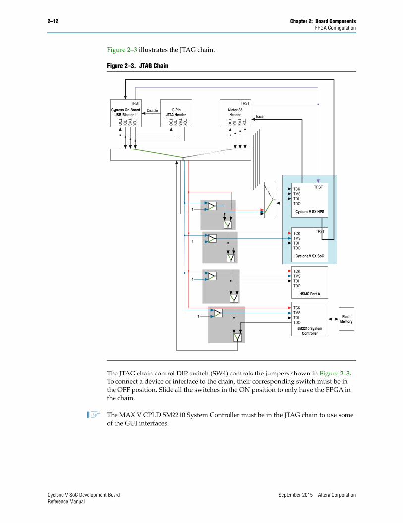
Figure 2–3 illustrates the JTAG chain.
The JTAG chain control DIP switch (SW4) controls the jumpers shown in Figure 2–3. To connect a device or interface to the chain, their corresponding switch must be in the OFF position. Slide all the switches in the ON position to only have the FPGA in the chain.
1 The MAX V CPLD 5M2210 System Controller must be in the JTAG chain to use some of the GUI interfaces.
Figure 2–3. JTAG Chain
1
1
1
1
Disable
TraceTCK
TMS
TDI
TDO
TRST
Cypress On-BoardUSB-Blaster II
TCK
TMS
TDI
TDO
10-PinJTAG Header
TCK
TMS
TDI
TDO
TRST
Mictor-38Header
TCKTMSTDITDO
TRST
Cyclone V SX HPS
TCKTMSTDITDO
TRST
Cyclone V SX SoC
TCKTMSTDITDO
HSMC Port A
TCKTMSTDITDO
5M2210 SystemController
FlashMemory
Cyclone V SoC Development Board September 2015 Altera CorporationReference Manual
Chapter 2: Board Components 2–13FPGA Configuration
The MAX II CPLD EPM570GF100I5N is dedicated to the on-board USB-Blaster II functionality only, connecting to the USB 2.0 PHY device on one side and drives JTAG signals out the other side on the GPIO pins. This device's own dedicated JTAG interface are routed to a small surface-mount header only intended for debugging of first article prototypes.
A USB 2.0 Cypress EZ-USB CY7C68013A device (U51) in a 56-pin VBGA package interfaces to a USB connector.
Table 2–5 lists the USB 2.0 PHY schematic signal names and their corresponding MAX II CPLD pin numbers.
Table 2–5. USB 2.0 PHY Schematic Signal Names and Functions (Part 1 of 2)
Board Reference (U51)
SchematicSignal Name
MAX II CPLD Pin Number I/O Standard Description
C1 24M_XTALIN — 3.3-V Crystal oscillator input
C2 24M_XTALOUT — 3.3-V Crystal oscillator output
E1 FX2_D_N — 3.3-V USB 2.0 PHY data
E2 FX2_D_P — 3.3-V USB 2.0 PHY data
H7 FX2_FLAGA D1 3.3-V Slave FIFO output status
G7 FX2_FLAGB G1 3.3-V Slave FIFO output status
H8 FX2_FLAGC C1 3.3-V Slave FIFO output status
G6 FX2_PA1 G3 3.3-V USB 2.0 PHY port A interface
F8 FX2_PA2 B1 3.3-V USB 2.0 PHY port A interface
F7 FX2_PA3 D2 3.3-V USB 2.0 PHY port A interface
F6 FX2_PA4 D3 3.3-V USB 2.0 PHY port A interface
C8 FX2_PA5 K4 3.3-V USB 2.0 PHY port A interface
C7 FX2_PA6 F2 3.3-V USB 2.0 PHY port A interface
C6 FX2_PA7 C2 3.3-V USB 2.0 PHY port A interface
H3 FX2_PB0 G2 3.3-V USB 2.0 PHY port B interface
F4 FX2_PB1 H8 3.3-V USB 2.0 PHY port B interface
H4 FX2_PB2 F3 3.3-V USB 2.0 PHY port B interface
G4 FX2_PB3 J3 3.3-V USB 2.0 PHY port B interface
H5 FX2_PB4 F1 3.3-V USB 2.0 PHY port B interface
G5 FX2_PB5 H1 3.3-V USB 2.0 PHY port B interface
F5 FX2_PB6 H7 3.3-V USB 2.0 PHY port B interface
H6 FX2_PB7 E1 3.3-V USB 2.0 PHY port B interface
A8 FX2_PD0 H3 3.3-V USB 2.0 PHY port D interface
A7 FX2_PD1 H2 3.3-V USB 2.0 PHY port D interface
B6 FX2_PD2 J2 3.3-V USB 2.0 PHY port D interface
A6 FX2_PD3 J1 3.3-V USB 2.0 PHY port D interface
B3 FX2_PD4 J6 3.3-V USB 2.0 PHY port D interface
A3 FX2_PD5 K3 3.3-V USB 2.0 PHY port D interface
C3 FX2_PD6 J5 3.3-V USB 2.0 PHY port D interface
A2 FX2_PD7 K2 3.3-V USB 2.0 PHY port D interface
September 2015 Altera Corporation Cyclone V SoC Development BoardReference Manual

2–14 Chapter 2: Board ComponentsFPGA Configuration
FPGA Programming from Flash MemoryFlash memory programming is possible through a variety of methods. The default method is to use the factory design—Golden Hardware Reference Design. This design contains an embedded web server, which serves the Board Update Portal web application. The web page allows you to link to SoC-related web pages and to control some user I/O and LCD on the development board.
On either power-up or by pressing the program configuration push button, PGM_CONFIG (S12), the MAX V CPLD 5M2210 System Controller's PFL configures the FPGA from the flash memory.
1 This feature is disabled by default. To enable this feature, slide the FACTORY_LOAD DIP switch (SW2.3) to the ON position.
The PFL megafunction reads 16-bit data from the flash memory and converts it to fast passive parallel (FPP) format. This 16-bit data is then written to the dedicated configuration pins in the FPGA during configuration.
Pressing the PGM_CONFIG push button (S12) loads the FPGA with a hardware page based on which PGM_LED[2:0] (D39, D40, D41) illuminates.
Table 2–6 lists the design that loads when you press the PGM_CONFIG push button.
B8 FX2_RESETN K9 3.3-V Embedded USB-Blaster hard reset
F3 FX2_SCL J4 3.3-V USB 2.0 PHY serial clock
G3 FX2_SDA — 3.3-V USB 2.0 PHY serial data
A1 FX2_SLRDN K1 3.3-V Read strobe for slave FIFO
B1 FX2_SLWRN J9 3.3-V Write strobe for slave FIFO
B7 FX2_WAKEUP — 3.3-V USB 2.0 PHY wake signal
G2 USB_B2_CLK E2 3.3-V USB 2.0 PHY 48-MHz interface clock
Table 2–5. USB 2.0 PHY Schematic Signal Names and Functions (Part 2 of 2)
Board Reference (U51)
SchematicSignal Name
MAX II CPLD Pin Number I/O Standard Description
Table 2–6. PGM_LED Settings (1)
PGM_LED0 (D41) PGM_LED1 (D40) PGM_LED2 (D39) Design
ON OFF OFF Factory hardware
OFF ON OFF User hardware 1
OFF OFF ON User hardware 2
Note to Table 2–6:
(1) ON indicates a setting of ’0’ while OFF indicates a setting of ’1’.
Cyclone V SoC Development Board September 2015 Altera CorporationReference Manual

Chapter 2: Board Components 2–15FPGA Configuration
Figure 2–4 shows the PFL configuration.
f For more information on the following topics, refer to the respective documents:
■ Board Update Portal, PFL design, and flash memory map storage, refer to the Cyclone V SoC Development Kit User Guide
■ PFL megafunction, refer to Parallel Flash Loader Megafunction User Guide.
FPGA Programming over External USB-BlasterThe JTAG chain header provides another method for configuring the FPGA using an external USB-Blaster device with the Quartus II Programmer running on a PC. To prevent contention between the JTAG masters, the embedded USB-Blaster is automatically disabled when you connect an external USB-Blaster to the JTAG chain through the JTAG chain header.
Figure 2–4. PFL Configuration
MAX V CPLD5M2210 System Controller
FPGA_DATA [3:0]
FPGA_DCLK
EPCQ_nCSFLASH_A [25:1]FLASH_D [15:0]
DATA [3:0]
DCLK
nSTATUSnCONFIGCONF_DONE
CONF_DONE
MSEL4MSEL3MSEL2MSEL1
MSEL[4:0] andBOOTSEL[3:0]also connects to theMAX V CPLD
2.5 V
10 kΩ
nCE
DATA [3:0]DCLKnCE
CFI Flash
FLASH_CEn
FLASH_OEnFLASH_WEn
FLASH_A [25:0]FLASH_D [15:0]
FLASH_CEnFLASH_OEnFLASH_WEn
FLASH_WPnFLASH_ADVn
FPGA_nCONFIGFPGA_CONF_DONE
FLASH_RYBSYn
FLASH_RYBSYn
FPGA_nSTATUS
2.5 V
10 kΩ
FLASH_ADVn
CVP_CONF_DONE
2.5 V
FLASH_CLK
FLASH_CLKFLASH_RSTn
FLASH_RESETn
FPGA_DATA [4] DATA [4]FPGA_DATA [7:5] DATA [7:5]
PS PORT
EPCQ
56.2 Ω
100 Ω56.2 Ω
56.2 Ω
50 MHz
100 MHz
INIT_DONECVP_CONFDONE
FPGA_INIT_DONEFPGA_CVP_DONE
2.5 V
2.5 V 2.5 V
MAX_ERROR
MAX_LOAD
FACTORY
USB_BLASTER
SECURITY_MODEFACTORY_LOADSi570_ENCLK125A_EN
MAX_RESETn
PGM_CONFIG
PGM_SEL
PGM_LED0
PGM_LED1
PGM_LED2
DIP
Sw
itch
BOOTSEL0BOOTSEL1BOOTSEL2
DIP Switch
DIP Switch
10 kΩ
Cyclone V SoC
September 2015 Altera Corporation Cyclone V SoC Development BoardReference Manual
2–16 Chapter 2: Board ComponentsStatus Elements
FPGA Programming using EPCQThe EPCQ device with non-volatile memory features a simple six-pin interface and a small form factor. The EPCQ supports AS x1 and x4 modes.
By default, this board has a FPP configuration scheme setting. The MAX_AS_CONF pin needs to be driven from the MAX V to enable the bus switch (U13) to isolate the EPCQ flash (U20) from the configuration bus. This happens when MSEL is 10010 or 10011.
In AS configuration scheme, the data will be read from the EPCQ flash directly to the FPGA. The MAX V CPLD 5M2210 System Controller controls the nCS line of the EPCQ to avoid line contention on DATA4 line due to functionality sharing. In order to program non-volatile memory, CFI Flash or EPCQ special programming functionality design should be loaded into the FPGA or MAX V CPLD to allow programming using the Quartus II Programmer.
Status ElementsThe development board includes status LEDs. This section describes the status elements.
Table 2–7 lists the LED board references, names, and functional descriptions.
Table 2–7. Board-Specific LEDs
Board Reference Schematic Signal Name I/O
Standard Description
D35 Power 5.0-V Blue LED. Illuminates when 5.0 V power is active.
D38 MAX_CONF_DONE 3.3-VGreen LED. Illuminates when the FPGA is successfully configured. Driven by the MAX V CPLD 5M2210 System Controller.
D36 MAX_ERROR 3.3-VRed LED. Illuminates when the MAX V CPLD 5M2210 System Controller fails to configure the FPGA. Driven by the MAX V CPLD 5M2210 System Controller.
D34 MAX_LOAD 3.3-VGreen LED. Illuminates when the MAX V CPLD 5M2210 System Controller is actively configuring the FPGA. Driven by the MAX V CPLD 5M2210 System Controller.
D41
D40
D39
PGM_LED[0]
PGM_LED[1]
PGM_LED[2]
3.3-V Green LEDs. Illuminates to indicate which hardware page loads from flash memory when you press the PGM_SEL push button.
D37 CVP_CONF_DONE 2.5-VGreen LED. Illuminates when the FPGA is successfully configured using CvP. Driven by the MAX V CPLD 5M2210 System Controller.
D9 HSMA_PRSNTn 2.5-VGreen LED. Illuminates when HSMC port A has a board or cable plugged-in such that pin 160 becomes grounded. Driven by the add-in card.
D30, D31
D29, D28
JTAG_RX, JTAG_TX
SC_RX, SC_TX1.8-V Green LEDs. Illuminates to indicate USB-Blaster II receive and
transmit activities.
D15, D14 UART_RX_LED, UART_TX_LED 3.3-V Green LED. Illuminates to indicate UART receive and transmit activities.
Cyclone V SoC Development Board September 2015 Altera CorporationReference Manual

Chapter 2: Board Components 2–17Setup Elements
Setup ElementsThe development board includes several different kinds of setup elements. This section describes the following setup elements:
■ Board settings DIP switch
■ JTAG chain control DIP switch
■ FPGA configuration mode DIP switch
■ HPS jumpers
■ CPU reset push button
■ MAX V reset push button
■ Program configuration push button
■ Program select push button
f For more information about the default settings of the DIP switches, refer to the Cyclone V SoC Development Kit User Guide.
Board Settings DIP SwitchThe board settings DIP switch (SW2) controls various features specific to the board and the MAX V CPLD 5M2210 System Controller logic design. Table 2–8 lists the switch controls and descriptions.
Table 2–8. Board Settings DIP Switch Controls
Switch Schematic Signal Name Description
1 CLK125A_ENON: Select programmable oscillator clock
OFF: Select SMA input clock
2 Si570_ENON: Disable on-board oscillator
OFF: Enable on-board oscillator
3 FACTORY_LOADON: Load the factory design from flash at power up.
OFF: Disable the PFL and do not configure from flash.
4 SECURITY_MODE
ON: Embedded USB-Blaster II sends FACTORY command at power up.
OFF: Embedded USB-Blaster II will not send FACTORY command at power up.
September 2015 Altera Corporation Cyclone V SoC Development BoardReference Manual
2–18 Chapter 2: Board ComponentsSetup Elements
JTAG Chain Control DIP SwitchThe JTAG chain control DIP switch (SW4) either removes or includes devices in the active JTAG chain. Table 2–9 lists the switch controls and its descriptions.
FPGA Configuration Mode DIP SwitchThe FPGA configuration mode DIP switch (SW3) defines the mode to use to configure the FPGA. Table 2–10 lists the switch controls and its descriptions. All switches at the ON position will select the default FPP x16 mode.
Table 2–9. JTAG Chain Control DIP Switch
Switch Schematic Signal Name Description
1 HPS_JTAG_ENON: Bypass Cyclone V HPS in the chain
OFF: Cyclone V HPS in-chain
2 FPGA_JTAG_ENON: Bypass Cyclone V FPGA in the chain
OFF: Cyclone V FPGA in-chain
3 HSMA_JTAG_ENON: Bypass HSMC port in the chain
OFF: HSMC port in-chain
4 MAX_JTAG_ENON: Bypass MAX V CPLD 5M2210 System Controller in the chain
OFF: MAX V CPLD 5M2210 System Controller in-chain
Table 2–10. FPGA Configuration Mode DIP Switch
Switch Schematic Signal Name Description
1 MSEL0ON: Select logic 0
OFF: Select logic 1
2 MSEL1ON: Select logic 0
OFF: Select logic 1
3 MSEL2ON: Select logic 0
OFF: Select logic 1
4 MSEL3ON: Select logic 0
OFF: Select logic 1
Cyclone V SoC Development Board September 2015 Altera CorporationReference Manual

Chapter 2: Board Components 2–19Setup Elements
HPS JumpersThe HPS jumpers define the bootstrap options for the HPS—boot source, mode, HPS clocks settings, POR mode and peripherals selection.
Table 2–11 lists the jumper settings and its descriptions.
CPU Reset Push ButtonThe CPU reset push button, CPU_RESETn (S10), is an input to the Cyclone V HPS pin and is an open-drain I/O from the MAX V CPLD System Controller. This push button is the default reset for both the HPS and CPLD logic. The MAX II CPLD 5M2210 also drives this push button during power-on-reset (POR).
Table 2–11. HPS Jumpers
Board Reference
Schematic Signal Name Description
J28, J29, J30 BOOTSEL[0:2]
Selects the boot mode and source for the HPS.
■ 0x0—Reserved
■ 0x1—FPGA (HPS-to-FPGA bridge)
■ 0x2—1.8 V NAND flash
■ 0x3—3.0 V NAND flash
■ 0x4—1.8 V SD/MMC flash memory with external transceiver
■ 0x5—3.0 V SD/MMC flash memory with internal transceiver
■ 0x6—1.8 V SPI or quad SPI flash memory
■ 0x7—3.0 V SPI or quad SPI flash memory
J26, J27 CLKSEL[0:1]Selects the HPS clock settings. The actual clock settings are also dependent on BOOTSEL[0:2].
J13 OSC1_CLK_SEL
Selects the source of OSC1 clock.
■ ON: Select on-board clock generator.
■ OFF: Select external source via SMA connector.
J31 LTC_EXP_SPI_I2C
Selects the LTC expansion header interface type.
■ ON: Select SPI.
■ OFF: Select I2C.
J6 JTAG_HPS_SEL
HPS in JTAG chain or only connect HPS to MICTOR.
Selects the source to control the HPS.
■ ON: Select on-board USB-Blaster II as the JTAG master.
■ OFF: Select MICTOR-based JTAG master, such as DSTREAM or Lauterbach programming cables. Also, sets SW4.1 to ON to remove the on-board USB Blaster II from driving the HPS JTAG input port in this mode.
J7 JTAG_SEL
Selects the source of the JTAG chain.
■ ON: Select on-board USB-Blaster II as the source.
■ OFF: Select MICTOR as the source.
September 2015 Altera Corporation Cyclone V SoC Development BoardReference Manual

2–20 Chapter 2: Board ComponentsGeneral User Input/Output
MAX V Reset Push ButtonThe MAX V reset push button, MAX_RESETn (S2), is an input to the MAX V CPLD 5M2210 System Controller. This push button is the default reset for the CPLD logic.
Program Configuration Push ButtonThe program configuration push button, PGM_CONFIG (S12), is an input to the MAX V CPLD 5M2210 System Controller. This input forces a FPGA reconfiguration from the flash memory. The location in the flash memory is based on the settings of PGM_LED[2:0], which is controlled by the program select push button, PGM_SEL (S2). Valid settings include PGM_LED0, PGM_LED1, or PGM_LED2 on the three pages in flash memory reserved for FPGA designs.
Program Select Push ButtonThe program select push button, PGM_SEL (S11), is an input to the MAX V CPLD System Controller. This push button toggles the PGM_LED[2:0]sequence that selects which location in the flash memory is used to configure the FPGA. Refer to Table 2–6 on page 2–14 for the PGM_LED[2:0] sequence definitions.
Mictor JumperThe Mictor jumper (J39) defines the function pin 14 on the external 38-pin Mictor connector. If J39 is shorted, pin 14 is powered by the 3.3-V power rail. If J39 is open, pin 14 floats.
General User Input/OutputThis section describes the user I/O interface to the FPGA, including the push buttons, DIP switches, LEDs, expansion header, and character LCD.
User-Defined Push ButtonsThe development board includes six user-defined push buttons. For information about the system and safe reset push buttons, refer to “Setup Elements” on page 2–17.
Board references S1–S6 are push buttons for controlling the FPGA designs that loads into the Cyclone V SoC device. Push buttons S5 and S6 connect to the FPGA while push buttons S1–S4 connect to the HPS. When you press and hold down the switch, the device pin is set to logic 0; when you release the switch, the device pin is set to logic 1. There are no board-specific functions for these general user push buttons.
Table 2–12 lists the user-defined push button schematic signal names and their corresponding Cyclone V SoC pin numbers.
Table 2–12. User-Defined Push Button Schematic Signal Names and Functions
Board Reference Schematic Signal Name Cyclone V SoC Pin Number I/O Standard
S6 USER_PB_FPGA0 AA13 1.5-V
S5 USER_PB_FPGA1 AB13 1.5-V
Cyclone V SoC Development Board September 2015 Altera CorporationReference Manual

Chapter 2: Board Components 2–21General User Input/Output
S4 USER_PB_HPS0 T30 2.5-V
S3 USER_PB_HPS1 U28 2.5-V
S2 USER_PB_HPS2 T21 2.5-V
S1 USER_PB_HPS3 U20 2.5-V
Table 2–12. User-Defined Push Button Schematic Signal Names and Functions
Board Reference Schematic Signal Name Cyclone V SoC Pin Number I/O Standard
September 2015 Altera Corporation Cyclone V SoC Development BoardReference Manual
2–22 Chapter 2: Board ComponentsGeneral User Input/Output
User-Defined DIP SwitchBoard reference SW1 is a eight-pin DIP switch. This switch is user-defined and provides additional FPGA or HPS input control. When the switch is in the OFF position, a logic 1 is selected. When the switch is in the ON position, a logic 0 is selected. There are no board-specific functions for this switch.
Table 2–13 lists the user-defined DIP switch schematic signal names and their corresponding Cyclone V SoC pin numbers.
User-Defined LEDsBoard references D1–D8 are eight user-defined LEDs. The status and debugging signals are driven to the LEDs from the FPGA or HPS designs loaded into the Cyclone V SoC. Driving a logic 0 on the I/O port turns the LED on while driving a logic 1 turns the LED off. There are no board-specific functions for these LEDs.
Table 2–14 lists the general LED schematic signal names and their corresponding Cyclone V SoC pin numbers.
Table 2–13. User-Defined DIP Switch Schematic Signal Names and Functions
Board Reference SchematicSignal Name
Cyclone V SoCPin Number I/O Standard
1 USER_DIPSW_HPS0 N30 3.3-V
2 USER_DIPSW_HPS1 P29 3.3-V
3 USER_DIPSW_HPS2 P22 3.3-V
4 USER_DIPSW_HPS3 V20 3.3-V
5 USER_DIPSW_FPGA0 AG10 2.5-V
6 USER_DIPSW_FPGA1 AH9 2.5-V
7 USER_DIPSW_FPGA2 AF11 2.5-V
8 USER_DIPSW_FPGA3 AG11 2.5-V
Table 2–14. General LED Schematic Signal Names and Functions
Board Reference SchematicSignal Name
Cyclone V SoCPin Number I/O Standard
D8 USER_LED_FPGA0 AK2 2.5-V
D7 USER_LED_FPGA1 Y16 2.5-V
D6 USER_LED_FPGA2 W15 2.5-V
D5 USER_LED_FPGA3 AB17 2.5-V
D4 USER_LED_HPS0 E17 3.3-V
D3 USER_LED_HPS1 E18 3.3-V
D2 USER_LED_HPS2 G17 3.3-V
D1 USER_LED_HPS3 C18 3.3-V
Cyclone V SoC Development Board September 2015 Altera CorporationReference Manual

Chapter 2: Board Components 2–23General User Input/Output
Expansion HeaderThe development board includes an expansion header (J23) to connect a daughter card from Linear Technology. The interface connects to the SPI master or I2C ports of the HPS to allow bidirectional communication with two types of protocols. The 14-pin header also allows GPIO, SPI, and I2C extension for user purposes if there are no interface card available.
The LTC_EXP_SPI_I2C jumper (J31) sets the interfaces type. When J31 is shunted, SPI interface is used. When J31 is not shunted, I2C interface is used.
Character LCD The development board includes a single 10-pin 0.1" pitch single-row header that interfaces to a 2 line × 16 character Lumex character LCD using standard I2C interface connected to the HPS. The character LCD has a two headers that mount directly to the board's 10-pin header, so it can be easily removed for access to components under the display. You can also use the header for debugging, I2C expansion, or other purposes.
f For more information such as timing, character maps, interface guidelines, and other related documentation, visit www.lumex.com.
September 2015 Altera Corporation Cyclone V SoC Development BoardReference Manual

2–24 Chapter 2: Board ComponentsClock Circuitry
Clock CircuitryThis section describes the board's clock inputs and outputs.
On-Board OscillatorsFigure 2–5 shows the default frequencies of all external clocks going to the Cyclone V SoC development board.
Table 2–15 lists the on-board clock inputs for the development board.
Figure 2–5. Cyclone V SoC Development Board Clocks
Cyclone V SX C6
Bank 8 HPS Peripherals
HPS Core
HPS
Mem
ory
Inte
rface
Bank
5
Bank 3 Bank 4
Bank
0L
Bank
1L
Bank
2L
REFCLK2Lp/nSi570
100 MHz/I2C
REFCLK1Lp/nSi571
148.5 MHz/I2C
REFCLK0Lp/nSi52112
100 MHz
PCIeSocket
Si5338OSC1_CLK_SYN, 25 MHz
CLK5p, 156.25 MHz
CLK5n, 100 MHz
25 MHz
CLK2p, 25 MHzCLK0p100 MHz
SL18860C50 MHz
PHYuPD60620CLK4p/n
HSMC ConnectorHS
MA_C
LK_IN
0
HSMA
_CLK
_IN_P
/N2
OSC1_CLK_SMA, 25 MHZ
125 MHz
100 MHz MAX V
MAX V
HSMA
_CLK
_OUT
0
HSMA
_CLK
_OUT
_P/N
2
HSMA
_CLK
_OUT
_P/N
1HS
MA_C
LK_IN
_P/N
1
Si5335
50 MHz
HPS_CLK2, 25 MHz
ICS83054
SMA
CLK3p50 MHz
HPS_CLK125 MHz
Table 2–15. On-Board Clock Inputs (Part 1 of 2)
Source Schematic Signal Name
I/O Standard
Cyclone V SoC Pin Number Description
X1 REFCLK_QL2_P LVDS P9 100 MHz programmable oscillator driving transceiver bank QL2 REFCLK input for HSMA signals.
X3 CLK_148_P LVTTL T9 148.5 MHz programmable VCXO driving transceiver bank QL1 REFCLK input for SDI video signals or SMA.
X5 CLK_ENET_FPGA_P 2.5-V Y26 125 MHz fixed oscillator driving CLK4p in bank 5B.
U49 PCIE_REFCLK_QL0_P HSCL W8 100 MHz fixed oscillator driving transceiver bank QL1 REFCLK input for PCI Express.
Cyclone V SoC Development Board September 2015 Altera CorporationReference Manual

Chapter 2: Board Components 2–25Clock Circuitry
Off-Board Input/Output ClockThe development board has input and output clocks which can be driven onto the board. The output clocks can be programmed to different levels and I/O standards according to the FPGA device’s specification.
Table 2–16 lists the clock inputs for the development board.
U35
CLK_ENET_FPGA_PHY 1.5-V AA16 25 MHz fixed oscillator driving CLK2p in bank 4A
CLK_DUAL_ENET_PHY 1.5-V — 25MHz fixed oscillator driving the Renesas dual ethernet PHY (U45).
CLK_100M_MAX 1.5-V — 100MHz fixed oscillator driving the MAX V CPLDpin J5 for FPGA configuration and other logic.
CLK_100M_FPGA 2.5-V AB27 100 MHz fixed oscillator driving CLK5n in bank 5B.
U29
CLK_BOT1 1.5-V AF14 100 MHz programmable oscillator driving CLK0p in bank 3B for FPGA DDR3 or other logic.
CLK_TOP1 2.5-V AA26 156.25 MHz programmable oscillator driving CLK5p in Bank 5B.
CLK_OSC1 2.5-V D25 25 MHz programmable oscillator driving HPS_CLK1 for the HPS in bank 7A though SMA/XO multiplexer (U52).
CLK_OSC2 2.5-V F25 25 MHz programmable oscillator driving HPS_CLK2 for the HPS in bank 7A.
X4CLK_50M_MAX 1.8-V — 50 MHz fixed oscillator driving the MAX V CPLD pin
J12 for FPGA configuration or other logic.
CLK_50M_FPGA 1.5-V AC18 50 MHz fixed oscillator driving CLK3p in bank 4A for general logic.
Table 2–15. On-Board Clock Inputs (Part 2 of 2)
Source Schematic Signal Name
I/O Standard
Cyclone V SoC Pin Number Description
Table 2–16. Off-Board Clock Inputs
Source Schematic Signal Name I/O Standard Cyclone V SoC
Pin Number Description
SMA CLKIN_SMA_HPS 2.5-V CMOS — Multiplexed clock input to OSC1 of the HPS
Samtec HSMC HSMA_CLK_IN0 LVTTL K14 Single-ended input from the installed HSMC cable or board.
Samtec HSMCHSMA_CLK_IN_P1 LVTTL AG2 LVTTL input from the installed HSMC cable or
board.HSMA_CLK_IN_N1 LVTTL AH3
Samtec HSMCHSMA_CLK_IN_P2 LVDS/LVTTL H15 LVDS input from the installed HSMC cable or
board. Can also support 2x LVTTL inputs.HSMA_CLK_IN_N2 LVDS/LVTTL G15
September 2015 Altera Corporation Cyclone V SoC Development BoardReference Manual

2–26 Chapter 2: Board ComponentsComponents and Interfaces
Table 2–17 lists the clock outputs for the development board.
Components and InterfacesThis section describes the development board's communication ports and interface cards relative to the Cyclone V SoC device. The development board supports the following communication ports:
■ PCI Express
■ 10/100/1000 Ethernet (HPS)
■ 10/100 Ethernet (FPGA)
■ HSMC
■ RS-232 Serial UART (HPS)
■ CAN bus (HPS)
■ Real-Time clock (HPS)
■ SPI master
■ I2C
■ SDI video
PCI ExpressThe PCI Express interface on the development board supports auto-negotiating channel width from ×1 to ×4 as well as the connection speed of Gen1 at 2.5 Gbps/lane for a maximum of 10 Gbps bandwidth.
The PCIE_REFCLK_P/N signal is a 100-MHz differential input that is driven to the daughter card through the PCI Express edge connector. This signal connects directly to a Cyclone V SoC REFCLK input pin pair using DC coupling. The I/O standard is High-Speed Current Steering Logic (HCSL).
Table 2–17. Off-Board Clock Outputs
Source Schematic Signal Name I/O Standard Cyclone V SoC
Pin Number Description
Samtec HSMC HSMA_CLK_OUT0 2.5-V CMOS A10 FPGA CMOS output (or GPIO)
Samtec HSMCHSMA_CLK_OUT_P1 2.5-V CMOS AJ2
CMOS outputHSMA_CLK_OUT_N1 2.5-V CMOS AC12
Samtec HSMCHSMA_CLK_OUT_P2 LVDS/2.5V CMOS E7 LVDS output. Can also support 2x CMOS
outputs.HSMA_CLK_OUT_N2 LVDS/2.5V CMOS E6
PCI Express Socket
PCIE_REFCLK_QL0_P HCSL W8HCSL output to the PCI Express socket
PCIE_REFCLK_QL0_N HCSL W7
Cyclone V SoC Development Board September 2015 Altera CorporationReference Manual

Chapter 2: Board Components 2–27Components and Interfaces
Figure 2–6 shows the PCI Express reference clock levels.
By default, the Cyclone V SoC development board is set up for the PCI Express interface to use with the Cyclone V SoC device in root-port mode, such as when plugging in a PCI Express add-in card into the PCI Express socket (J25). In this case, the switching regulator generates and drives the clock to both the Cyclone V SoC device and the add-in card.
To use the PCI Express interface with the Cyclone V SoC device in end-point mode, for example, with a cable plugged into a PC, you must remove resistors R253, R254, R249, and R251, and install R250 and R252. This resistor change will route the clock from the PC directly into the Cyclone V SoC device. You can use a PCI Express gen1x4 cable from Samtec (HDR-172378-02-PCIEC) for this connection.
1 This cable connects power (3.3 V and 12 V) from the PC to the development board and therefore the development board's power needs to be isolated to function properly. To isolate the power, remove the development board's power isolation resistors, R554 and R547, located near the PCI Express connector. The ground pin (GND) will still connect through the cable as it is required for normal operation.
The PCI Express edge connector also has a presence detect feature for the motherboard to determine if a card is installed. A jumper is provided to optionally connect PRSNT1n to any of the three PRSNT2n pins found within the x4 connector definition. This is to address issues on some PC systems that would base the link-width capability on the presence detect pins versus a query operation.
Table 2–18 summarizes the PCI Express pin assignments. The signal names and directions are relative to the Cyclone V SoC.
Figure 2–6. PCI Express Reference Clock Levels
VMAX = 1.15 V
VCROSS MAX = 550 mV
VCROSS MIN = 250 mV
VMIN = –0.30 V
REFCLK –
REFCLK +
Table 2–18. PCI Express Pin Assignments, Schematic Signal Names, and Functions (Part 1 of 2)
Board Reference (J18)
Schematic Signal Name I/O Standard Cyclone V SoC Device
Pin Number Description
A11 PCIE_PERSTN LVTTL AG6 Reset
B17 PCIE_PRSNT2N_X1 LVTTL AD29 Presence detect DIP switch
B31 PCIE_PRSNT2N_X4 LVTTL A11 Presence detect DIP switch
A14 PCIE_REFCLK_SYN_N HCSL W7 Motherboard reference clock
A13 PCIE_REFCLK_SYN_P HCSL W8 Motherboard reference clock
B5 PCIE_SMCLK LVTTL AE29 SMB clock
B6 PCIE_SMDAT LVTTL J14 SMB data
September 2015 Altera Corporation Cyclone V SoC Development BoardReference Manual

2–28 Chapter 2: Board ComponentsComponents and Interfaces
10/100/1000 Ethernet (HPS)The development board supports an RJ-45 10/100/1000 base-T Ethernet using an external Micrel KSZ9021RN PHY and the HPS EMAC. The PHY-to-MAC interface employs RGMII connection using four data lines at 250 Mbps each for a connection speed of 1 Gbps.
The Micrel KSZ9021RN PHY uses 2.5-V or 3.3-V power rails. The PHY interfaces to an RJ-45 model with internal magnetics that can be used for driving copper lines with Ethernet traffic.
Figure 2–7 shows the RGMII interface between the FPGA (MAC) and Micrel KSZ9021RN PHY.
B11 PCIE_WAKEN LVTTL W21 Wake signal
A17 PCIE_RX_N0 1.5-V PCML AE1 Receive bus
A22 PCIE_RX_N1 1.5-V PCML AC1 Receive bus
A26 PCIE_RX_N2 1.5-V PCML AA1 Receive bus
A30 PCIE_RX_N3 1.5-V PCML W1 Receive bus
A16 PCIE_RX_P0 1.5-V PCML AE2 Receive bus
A21 PCIE_RX_P1 1.5-V PCML AC2 Receive bus
A25 PCIE_RX_P2 1.5-V PCML AA2 Receive bus
A29 PCIE_RX_P3 1.5-V PCML W2 Receive bus
B15 PCIE_TX_N0 1.5-V PCML AD3 Transmit bus
B20 PCIE_TX_N1 1.5-V PCML AB3 Transmit bus
B24 PCIE_TX_N2 1.5-V PCML Y3 Transmit bus
B28 PCIE_TX_N3 1.5-V PCML V3 Transmit bus
B14 PCIE_TX_P0 1.5-V PCML AD4 Transmit bus
B19 PCIE_TX_P1 1.5-V PCML AB4 Transmit bus
B23 PCIE_TX_P2 1.5-V PCML Y4 Transmit bus
B27 PCIE_TX_P3 1.5-V PCML V4 Transmit bus
Table 2–18. PCI Express Pin Assignments, Schematic Signal Names, and Functions (Part 2 of 2)
Board Reference (J18)
Schematic Signal Name I/O Standard Cyclone V SoC Device
Pin Number Description
Figure 2–7. RGMII Interface between FPGA (MAC) and PHY
RGMIIMAC
Single-Port RGMIIMicrel KSZ9021RN
RJ-45
Cyclone V SoC Development Board September 2015 Altera CorporationReference Manual
Chapter 2: Board Components 2–29Components and Interfaces
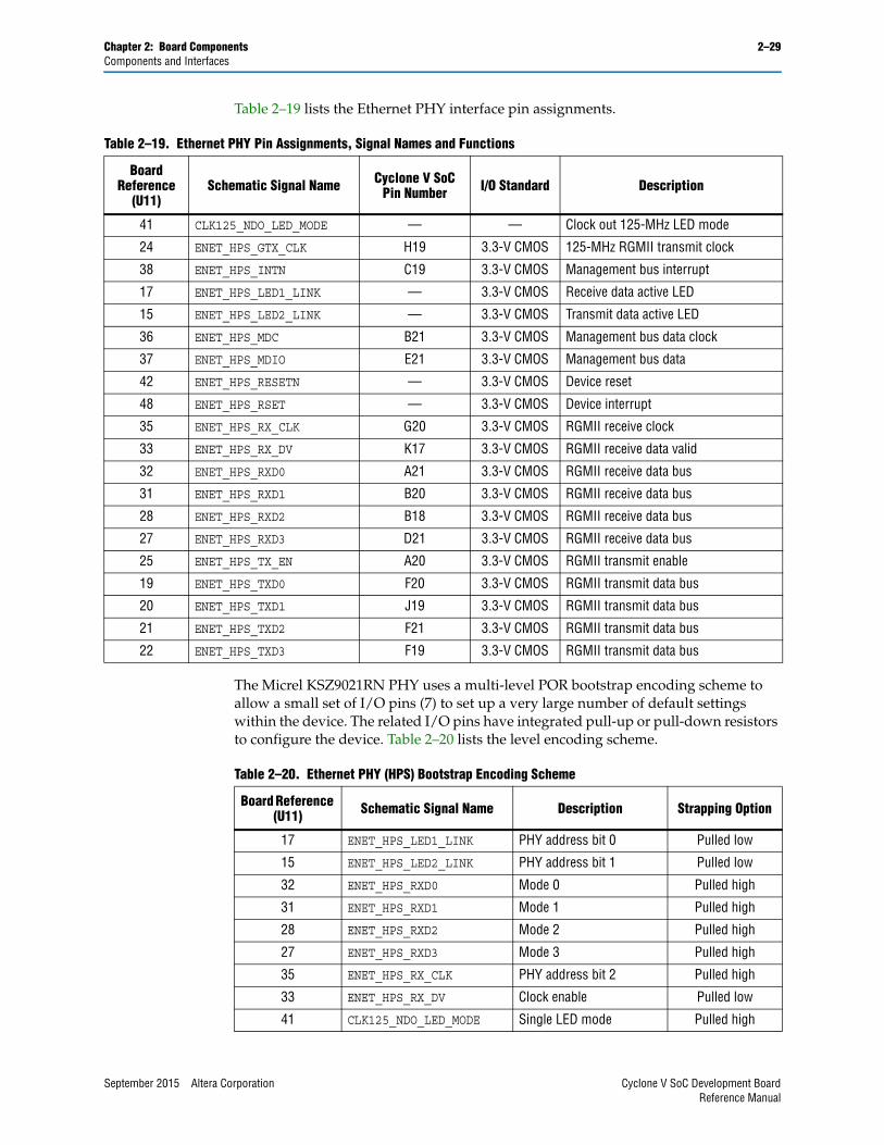
Table 2–19 lists the Ethernet PHY interface pin assignments.
The Micrel KSZ9021RN PHY uses a multi-level POR bootstrap encoding scheme to allow a small set of I/O pins (7) to set up a very large number of default settings within the device. The related I/O pins have integrated pull-up or pull-down resistors to configure the device. Table 2–20 lists the level encoding scheme.
Table 2–19. Ethernet PHY Pin Assignments, Signal Names and Functions
Board Reference
(U11)Schematic Signal Name Cyclone V SoC
Pin Number I/O Standard Description
41 CLK125_NDO_LED_MODE — — Clock out 125-MHz LED mode
24 ENET_HPS_GTX_CLK H19 3.3-V CMOS 125-MHz RGMII transmit clock
38 ENET_HPS_INTN C19 3.3-V CMOS Management bus interrupt
17 ENET_HPS_LED1_LINK — 3.3-V CMOS Receive data active LED
15 ENET_HPS_LED2_LINK — 3.3-V CMOS Transmit data active LED
36 ENET_HPS_MDC B21 3.3-V CMOS Management bus data clock
37 ENET_HPS_MDIO E21 3.3-V CMOS Management bus data
42 ENET_HPS_RESETN — 3.3-V CMOS Device reset
48 ENET_HPS_RSET — 3.3-V CMOS Device interrupt
35 ENET_HPS_RX_CLK G20 3.3-V CMOS RGMII receive clock
33 ENET_HPS_RX_DV K17 3.3-V CMOS RGMII receive data valid
32 ENET_HPS_RXD0 A21 3.3-V CMOS RGMII receive data bus
31 ENET_HPS_RXD1 B20 3.3-V CMOS RGMII receive data bus
28 ENET_HPS_RXD2 B18 3.3-V CMOS RGMII receive data bus
27 ENET_HPS_RXD3 D21 3.3-V CMOS RGMII receive data bus
25 ENET_HPS_TX_EN A20 3.3-V CMOS RGMII transmit enable
19 ENET_HPS_TXD0 F20 3.3-V CMOS RGMII transmit data bus
20 ENET_HPS_TXD1 J19 3.3-V CMOS RGMII transmit data bus
21 ENET_HPS_TXD2 F21 3.3-V CMOS RGMII transmit data bus
22 ENET_HPS_TXD3 F19 3.3-V CMOS RGMII transmit data bus
Table 2–20. Ethernet PHY (HPS) Bootstrap Encoding Scheme
Board Reference (U11) Schematic Signal Name Description Strapping Option
17 ENET_HPS_LED1_LINK PHY address bit 0 Pulled low
15 ENET_HPS_LED2_LINK PHY address bit 1 Pulled low
32 ENET_HPS_RXD0 Mode 0 Pulled high
31 ENET_HPS_RXD1 Mode 1 Pulled high
28 ENET_HPS_RXD2 Mode 2 Pulled high
27 ENET_HPS_RXD3 Mode 3 Pulled high
35 ENET_HPS_RX_CLK PHY address bit 2 Pulled high
33 ENET_HPS_RX_DV Clock enable Pulled low
41 CLK125_NDO_LED_MODE Single LED mode Pulled high
September 2015 Altera Corporation Cyclone V SoC Development BoardReference Manual

2–30 Chapter 2: Board ComponentsComponents and Interfaces
10/100 Ethernet (FPGA)The development board supports an RJ-45 10/100 base-T Ethernet using an external Renesas uPD60620A PHY. This PHY supports EtherCAT, Ethernet IRT and DLR features using 3rd party MAC IP. The PHY-to-MAC interface employs MII connection using four data lines at 25 Mbps each for a connection speed of 100 Mbps.
The PHY uses 3.3-V power rails and requires a 25 MHz reference clock to be driven from a dedicated oscillator. The PHY interfaces to a dual RJ-45 model with internal magnetics that can be used for driving copper lines with Ethernet traffic.
Figure 2–7 shows the MII interface between the FPGA (MAC) and Renesas uPD60620A PHY.
Table 2–21 lists the Ethernet PHY interface pin assignments.
Figure 2–8. MII Interface between FPGA (MAC) and PHY
FPGA MIIMAC
Dual-Port RGMIIRenesas
uPD60620A
RJ-45
RJ-45
Table 2–21. Ethernet PHY Pin Assignments, Signal Names and Functions (Part 1 of 2)
Board Reference
(U45)Schematic Signal Name Cyclone V SoC
Pin Number I/O Standard Description
68 ENET1_ACT_LED — 2.5-V Receive data active LED
69 ENET1_LINK_LED — 2.5-V Transmit data active LED
18 ENET1_MDI_RX_N — 2.5-V Media dependent interface
17 ENET1_MDI_RX_P — 2.5-V Media dependent interface
16 ENET1_MDI_TX_N — 2.5-V Media dependent interface
15 ENET1_MDI_TX_P — 2.5-V Media dependent interface
59 ENET1_RX_CLK Y24 2.5-V MII receive clock
53 ENET1_RX_D0 AB23 2.5-V MII receive data bus
54 ENET1_RX_D1 AA24 2.5-V MII receive data bus
55 ENET1_RX_D2 AB25 2.5-V MII receive data bus
56 ENET1_RX_D3 AE27 2.5-V MII receive data bus
57 ENET1_RX_DV Y23 2.5-V MII receive data valid
58 ENET1_RX_ERROR AE28 2.5-V MII receive error
49 ENET1_TX_CLK_FB W25 2.5-V 25-MHz MII transmit clock
43 ENET1_TX_D0 W20 2.5-V MII transmit data bus
44 ENET1_TX_D1 Y21 2.5-V MII transmit data bus
45 ENET1_TX_D2 AA25 2.5-V MII transmit data bus
Cyclone V SoC Development Board September 2015 Altera CorporationReference Manual

Chapter 2: Board Components 2–31Components and Interfaces
The PHY uses a multi-level POR bootstrap encoding scheme to allow a small set of I/O pins to set up a very large number of default settings within the device. The related I/O pins have integrated pull-up or pull-down resistors to configure the device. To change the configuration, connect an external resistor of maximum 5 kΩ to the pin. Table 2–22 lists the level encoding scheme.
46 ENET1_TX_D3 AB26 2.5-V MII transmit data bus
48 ENET1_TX_EN AB22 2.5-V MII transmit enable
65 ENET2_ACT_LED — 2.5-V Receive data active LED
67 ENET2_LINK_LED — 2.5-V Transmit data active LED
4 ENET2_MDI_RX_N — 2.5-V Media dependent interface
5 ENET2_MDI_RX_P — 2.5-V Media dependent interface
6 ENET2_MDI_TX_N — 2.5-V Media dependent interface
7 ENET2_MDI_TX_P — 2.5-V Media dependent interface
41 ENET2_RX_CLK AH30 2.5-V MII receive clock
35 ENET2_RX_D0 AF29 2.5-V MII receive data bus
36 ENET2_RX_D1 AF30 2.5-V MII receive data bus
37 ENET2_RX_D2 AD26 2.5-V MII receive data bus
38 ENET2_RX_D3 AC27 2.5-V MII receive data bus
39 ENET2_RX_DV AC28 2.5-V MII receive data valid
40 ENET2_RX_ERROR V25 2.5-V MII receive error
29 ENET2_TX_CLK_FB AG30 2.5-V 25-MHz MII transmit clock
23 ENET2_TX_D0 AG27 2.5-V MII transmit data bus
24 ENET2_TX_D1 AG28 2.5-V MII transmit data bus
25 ENET2_TX_D2 AF28 2.5-V MII transmit data bus
26 ENET2_TX_D3 V23 2.5-V MII transmit data bus
28 ENET2_TX_EN W24 2.5-V MII transmit enable
1 ENET_DUAL_RESETN AJ1 2.5-V Device reset
62 ENET_FPGA_MDC H12 2.5-V Management bus data clock
63 ENET_FPGA_MDIO H13 2.5-V Management bus data
Table 2–21. Ethernet PHY Pin Assignments, Signal Names and Functions (Part 2 of 2)
Board Reference
(U45)Schematic Signal Name Cyclone V SoC
Pin Number I/O Standard Description
Table 2–22. Ethernet PHY (FPGA) Bootstrap Encoding Scheme (Part 1 of 2)
Board Reference (U11) Schematic Signal Name Description Strapping Option
36 ENET2_RX_D1Auto-negotiation disabled. 100 base-T default. Pulled low
35 ENET2_RX_D0 Full duplex operation Pulled high
41 ENET2_RX_CLK Disable quick auto negotiation Pulled low
58 ENET1_RX_ERROR MII mode operation Pulled low
59 ENET1_RX_CLK AUTOMDI-X enabled Pulled high
September 2015 Altera Corporation Cyclone V SoC Development BoardReference Manual

2–32 Chapter 2: Board ComponentsComponents and Interfaces
HSMCThe development board supports a HSMC interface (J12). The HSMC interface supports a full SPI4.2 interface (17 LVDS channels), two input and output clocks, as well as JTAG and SMB signals. The LVDS channels can be used for CMOS signaling or LVDS.
1 The HSMC is an Altera-developed open specification, which allows you to expand the functionality of the development board through the addition of daughtercards (HSMCs).
f For more information about the HSMC specification such as signaling standards, signal integrity, compatible connectors, and mechanical information, refer to the High Speed Mezzanine Card (HSMC) Specification manual.
The HSMC connector has a total of 172 pins, including 120 signal pins, 39 power pins, and 13 ground pins. The ground pins are located between the two rows of signal and power pins, acting both as a shield and a reference. The HSMC host connector is based on the 0.5 mm-pitch QSH/QTH family of high-speed, board-to-board connectors from Samtec. There are three banks in this connector. Bank 1 has every third pin removed as done in the QSH-DP/QTH-DP series. Bank 2 and bank 3 have all the pins populated as done in the QSH/QTH series. Since the Cyclone V SoC development board is not a transceiver board, the transceiver pins of the HSMC is not connected to the Cyclone V SoC device.
39 ENET2_RX_DV Transmit mode for PHY1 Pulled high
53 ENET1_RX_D0Auto-negotiation disabled. 10 base-T default. Pulled low
53 ENET1_RX_D0 Address for SMI Pulled low
54 ENET1_RX_D1 Address for SMI Pulled low
29 ENET2_TX_CLK_FBAsynchronous or synchronous mode for transmit clock Pulled high
Table 2–22. Ethernet PHY (FPGA) Bootstrap Encoding Scheme (Part 2 of 2)
Board Reference (U11) Schematic Signal Name Description Strapping Option
Cyclone V SoC Development Board September 2015 Altera CorporationReference Manual
Chapter 2: Board Components 2–33Components and Interfaces
Figure 2–9 shows the bank arrangement of signals with respect to the Samtec connector's three banks.
The HSMC interface has programmable bi-directional I/O pins that can be used as 2.5-V LVCMOS, which is 3.3-V LVTTL-compatible. These pins can also be used as various differential I/O standards including, but not limited to, LVDS, mini-LVDS, and RSDS with up to 17 full-duplex channels.
1 As noted in the High Speed Mezzanine Card (HSMC) Specification manual, LVDS and single-ended I/O standards are only guaranteed to function when mixed according to either the generic single-ended pin-out or generic differential pin-out.
Table 2–23 lists the HSMC interface pin assignments, signal names, and functions.
Figure 2–9. HSMC Signal and Bank Diagram
Bank 3 Power
D(79.40) -or-
LVDS CLKIN2, CLKOUT2
Bank 2 Power D(39:0)
-or- D[3:0] + LVDS
CLKIN1, CLKOUT1
Bank 14 TX Channels CDR4 RX Channels CDR
JTAGSMB
CLKIN0, CLKOUT0
Table 2–23. HSMC Interface Pin Assignments, Schematic Signal Names, and Functions (Part 1 of 4)
Board Reference (J12)
Schematic Signal Name
Cyclone V SoCPin Number I/O Standard Description
29 HSMA_TX_P0 P4 1.5-V PCML Transmit channel
30 HSMA_RX_P0 R2 1.5-V PCML Receive channel
31 HSMA_TX_N0 P3 1.5-V PCML Transmit channel
32 HSMA_RX_N0 R1 1.5-V PCML Receive channel
25 HSMA_TX_P1 M4 1.5-V PCML Transmit channel
26 HSMA_RX_P1 N2 1.5-V PCML Receive channel
27 HSMA_TX_N1 M3 1.5-V PCML Transmit channel
28 HSMA_RX_N1 N1 1.5-V PCML Receive channel
21 HSMA_TX_P2 K4 1.5-V PCML Transmit channel
22 HSMA_RX_P2 L2 1.5-V PCML Receive channel
23 HSMA_TX_N2 K3 1.5-V PCML Transmit channel
24 HSMA_RX_N2 L1 1.5-V PCML Receive channel
17 HSMA_TX_P3 H4 1.5-V PCML Transmit channel
18 HSMA_RX_P3 J2 1.5-V PCML Receive channel
September 2015 Altera Corporation Cyclone V SoC Development BoardReference Manual

2–34 Chapter 2: Board ComponentsComponents and Interfaces
19 HSMA_TX_N3 H3 1.5-V PCML Transmit channel
20 HSMA_RX_N3 J1 1.5-V PCML Receive channel
33 HSMA_SDA AH2 2.5-V CMOS Management serial clock
34 HSMA_SCL AA12 2.5-V CMOS Management serial data
35 JTAG_MUX_TCK — 2.5-V CMOS JTAG clock signal
36 JTAG_HSMA_TMS — 2.5-V CMOS JTAG mode select signal
37 JTAG_HSMA_TDO — 2.5-V CMOS JTAG data output
38 JTAG_HSMA_TDI — 2.5-V CMOS JTAG data input
39 HSMA_CLK_OUT0 A10 2.5-V CMOS Dedicated CMOS clock out
40 HSMA_CLK_IN0 K14 2.5-V CMOS Dedicated CMOS clock in
41 HSMA_D0 AF9 2.5-V CMOS Dedicated CMOS I/O bit 0
42 HSMA_D1 AF8 2.5-V CMOS Dedicated CMOS I/O bit 1
43 HSMA_D2 AG7 2.5-V CMOS Dedicated CMOS I/O bit 2
44 HSMA_D3 AG1 2.5-V CMOS Dedicated CMOS I/O bit 3
47 HSMA_TX_D_P0 E8 LVDS or 2.5-V LVDS TX bit 0 or CMOS bit 4
48 HSMA_RX_D_P0 H14 LVDS or 2.5-V LVDS RX bit 0 or CMOS bit 5
49 HSMA_TX_D_N0 D7 LVDS or 2.5-V LVDS TX bit 0n or CMOS bit 6
50 HSMA_RX_D_N0 G13 LVDS or 2.5-V LVDS RX bit 0n or CMOS bit 7
53 HSMA_TX_D_P1 D6 LVDS or 2.5-V LVDS TX bit 1 or CMOS bit 8
54 HSMA_RX_D_P1 K12 LVDS or 2.5-V LVDS RX bit 1 or CMOS bit 9
55 HSMA_TX_D_N1 C5 LVDS or 2.5-V LVDS TX bit 1n or CMOS bit 10
56 HSMA_RX_D_N1 J12 LVDS or 2.5-V LVDS RX bit 1n or CMOS bit 11
59 HSMA_TX_D_P2 E4 LVDS or 2.5-V LVDS TX bit 2 or CMOS bit 12
60 HSMA_RX_D_P2 J10 LVDS or 2.5-V LVDS RX bit 2 or CMOS bit 13
61 HSMA_TX_D_N2 D4 LVDS or 2.5-V LVDS TX bit 2n or CMOS bit 14
62 HSMA_RX_D_N2 J9 LVDS or 2.5-V LVDS RX bit 2n or CMOS bit 15
65 HSMA_TX_D_P3 E3 LVDS or 2.5-V LVDS TX bit 3 or CMOS bit 16
66 HSMA_RX_D_P3 K7 LVDS or 2.5-V LVDS RX bit 3 or CMOS bit 17
67 HSMA_TX_D_N3 E2 LVDS or 2.5-V LVDS TX bit 3n or CMOS bit 18
68 HSMA_RX_D_N3 K8 LVDS or 2.5-V LVDS RX bit 3n or CMOS bit 19
71 HSMA_TX_D_P4 E1 LVDS or 2.5-V LVDS TX bit 4 or CMOS bit 20
72 HSMA_RX_D_P4 G12 LVDS or 2.5-V LVDS RX bit 4 or CMOS bit 21
73 HSMA_TX_D_N4 D1 LVDS or 2.5-V LVDS TX bit 4n or CMOS bit 22
74 HSMA_RX_D_N4 G11 LVDS or 2.5-V LVDS RX bit 4n or CMOS bit 23
77 HSMA_TX_D_P5 D2 LVDS or 2.5-V LVDS TX bit 5 or CMOS bit 24
78 HSMA_RX_D_P5 J7 LVDS or 2.5-V LVDS RX bit 5 or CMOS bit 25
79 HSMA_TX_D_N5 C2 LVDS or 2.5-V LVDS TX bit 5n or CMOS bit 26
80 HSMA_RX_D_N5 H7 LVDS or 2.5-V LVDS RX bit 5n or CMOS bit 27
83 HSMA_TX_D_P6 B2 LVDS or 2.5-V LVDS TX bit 6 or CMOS bit 28
Table 2–23. HSMC Interface Pin Assignments, Schematic Signal Names, and Functions (Part 2 of 4)
Board Reference (J12)
Schematic Signal Name
Cyclone V SoCPin Number I/O Standard Description
Cyclone V SoC Development Board September 2015 Altera CorporationReference Manual
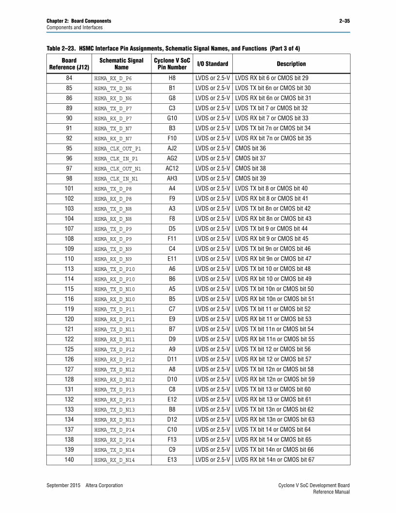
Chapter 2: Board Components 2–35Components and Interfaces
84 HSMA_RX_D_P6 H8 LVDS or 2.5-V LVDS RX bit 6 or CMOS bit 29
85 HSMA_TX_D_N6 B1 LVDS or 2.5-V LVDS TX bit 6n or CMOS bit 30
86 HSMA_RX_D_N6 G8 LVDS or 2.5-V LVDS RX bit 6n or CMOS bit 31
89 HSMA_TX_D_P7 C3 LVDS or 2.5-V LVDS TX bit 7 or CMOS bit 32
90 HSMA_RX_D_P7 G10 LVDS or 2.5-V LVDS RX bit 7 or CMOS bit 33
91 HSMA_TX_D_N7 B3 LVDS or 2.5-V LVDS TX bit 7n or CMOS bit 34
92 HSMA_RX_D_N7 F10 LVDS or 2.5-V LVDS RX bit 7n or CMOS bit 35
95 HSMA_CLK_OUT_P1 AJ2 LVDS or 2.5-V CMOS bit 36
96 HSMA_CLK_IN_P1 AG2 LVDS or 2.5-V CMOS bit 37
97 HSMA_CLK_OUT_N1 AC12 LVDS or 2.5-V CMOS bit 38
98 HSMA_CLK_IN_N1 AH3 LVDS or 2.5-V CMOS bit 39
101 HSMA_TX_D_P8 A4 LVDS or 2.5-V LVDS TX bit 8 or CMOS bit 40
102 HSMA_RX_D_P8 F9 LVDS or 2.5-V LVDS RX bit 8 or CMOS bit 41
103 HSMA_TX_D_N8 A3 LVDS or 2.5-V LVDS TX bit 8n or CMOS bit 42
104 HSMA_RX_D_N8 F8 LVDS or 2.5-V LVDS RX bit 8n or CMOS bit 43
107 HSMA_TX_D_P9 D5 LVDS or 2.5-V LVDS TX bit 9 or CMOS bit 44
108 HSMA_RX_D_P9 F11 LVDS or 2.5-V LVDS RX bit 9 or CMOS bit 45
109 HSMA_TX_D_N9 C4 LVDS or 2.5-V LVDS TX bit 9n or CMOS bit 46
110 HSMA_RX_D_N9 E11 LVDS or 2.5-V LVDS RX bit 9n or CMOS bit 47
113 HSMA_TX_D_P10 A6 LVDS or 2.5-V LVDS TX bit 10 or CMOS bit 48
114 HSMA_RX_D_P10 B6 LVDS or 2.5-V LVDS RX bit 10 or CMOS bit 49
115 HSMA_TX_D_N10 A5 LVDS or 2.5-V LVDS TX bit 10n or CMOS bit 50
116 HSMA_RX_D_N10 B5 LVDS or 2.5-V LVDS RX bit 10n or CMOS bit 51
119 HSMA_TX_D_P11 C7 LVDS or 2.5-V LVDS TX bit 11 or CMOS bit 52
120 HSMA_RX_D_P11 E9 LVDS or 2.5-V LVDS RX bit 11 or CMOS bit 53
121 HSMA_TX_D_N11 B7 LVDS or 2.5-V LVDS TX bit 11n or CMOS bit 54
122 HSMA_RX_D_N11 D9 LVDS or 2.5-V LVDS RX bit 11n or CMOS bit 55
125 HSMA_TX_D_P12 A9 LVDS or 2.5-V LVDS TX bit 12 or CMOS bit 56
126 HSMA_RX_D_P12 D11 LVDS or 2.5-V LVDS RX bit 12 or CMOS bit 57
127 HSMA_TX_D_N12 A8 LVDS or 2.5-V LVDS TX bit 12n or CMOS bit 58
128 HSMA_RX_D_N12 D10 LVDS or 2.5-V LVDS RX bit 12n or CMOS bit 59
131 HSMA_TX_D_P13 C8 LVDS or 2.5-V LVDS TX bit 13 or CMOS bit 60
132 HSMA_RX_D_P13 E12 LVDS or 2.5-V LVDS RX bit 13 or CMOS bit 61
133 HSMA_TX_D_N13 B8 LVDS or 2.5-V LVDS TX bit 13n or CMOS bit 62
134 HSMA_RX_D_N13 D12 LVDS or 2.5-V LVDS RX bit 13n or CMOS bit 63
137 HSMA_TX_D_P14 C10 LVDS or 2.5-V LVDS TX bit 14 or CMOS bit 64
138 HSMA_RX_D_P14 F13 LVDS or 2.5-V LVDS RX bit 14 or CMOS bit 65
139 HSMA_TX_D_N14 C9 LVDS or 2.5-V LVDS TX bit 14n or CMOS bit 66
140 HSMA_RX_D_N14 E13 LVDS or 2.5-V LVDS RX bit 14n or CMOS bit 67
Table 2–23. HSMC Interface Pin Assignments, Schematic Signal Names, and Functions (Part 3 of 4)
Board Reference (J12)
Schematic Signal Name
Cyclone V SoCPin Number I/O Standard Description
September 2015 Altera Corporation Cyclone V SoC Development BoardReference Manual

2–36 Chapter 2: Board ComponentsComponents and Interfaces
RS-232 UART (HPS)The development board supports a UART interface that connects to a USB connector (J8) using a FT232RQ-REEL USB-to-UART bridge. The maximum supported rate for this interface is 1 Mbps. Board reference D14 and D15 are the UART LEDs that illuminate to indicate TX and RX activity.
Table 2–32 lists the RS-232 UART pin assignments, signal names, and functions. The signal names and types are relative to the Cyclone V SoC in terms of I/O setting and direction.
CAN Bus (HPS)The development board supports one controller area network (CAN) bus through a DB-9 male connector. The CAN bus is multi-master broadcast serial bus standard for connecting electronic control units (ECUs). The maximum supported rate for this interface is 1 Mbps. This interface uses a dedicated CAN controller inside the HPS. A PHY device (U50) is connected in between the HPS and the DB-9 male connector.
143 HSMA_TX_D_P15 B13 LVDS or 2.5-V LVDS TX bit 15 or CMOS bit 68
144 HSMA_RX_D_P15 C13 LVDS or 2.5-V LVDS RX bit 15 or CMOS bit 69
145 HSMA_TX_D_N15 A13 LVDS or 2.5-V LVDS TX bit 15n or CMOS bit 70
146 HSMA_RX_D_N15 B12 LVDS or 2.5-V LVDS RX bit 15n or CMOS bit 71
149 HSMA_TX_D_P16 C12 LVDS or 2.5-V LVDS TX bit 16 or CMOS bit 72
150 HSMA_RX_D_P16 F15 LVDS or 2.5-V LVDS RX bit 16 or CMOS bit 73
151 HSMA_TX_D_N16 B11 LVDS or 2.5-V LVDS TX bit 16n or CMOS bit 74
152 HSMA_RX_D_N16 F14 LVDS or 2.5-V LVDS RX bit 16n or CMOS bit 75
155 HSMA_CLK_OUT_P2 E7 LVDS or 2.5-V LVDS or CMOS clock out 2 or CMOS bit 76
156 HSMA_CLK_IN_P2 H15 LVDS or 2.5-V LVDS or CMOS clock in 2 or CMOS bit 77
157 HSMA_CLK_OUT_N2 E6 LVDS or 2.5-V LVDS or CMOS clock out 2 or CMOS bit 78
158 HSMA_CLK_IN_N2 G15 LVDS or 2.5-V LVDS or CMOS clock in 2 or CMOS bit 79
160 HSMA_PRSNTN AD12 2.5-V CMOS HSMC port A presence detect
Table 2–23. HSMC Interface Pin Assignments, Schematic Signal Names, and Functions (Part 4 of 4)
Board Reference (J12)
Schematic Signal Name
Cyclone V SoCPin Number I/O Standard Description
Table 2–24. RS-232 UART Schematic Signal Names and Functions
Board Reference (U17)
SchematicSignal Name
Cyclone V SoC Pin Number I/O Standard Description
2 UART_TX D24 3.3-V Transmit data
30 UART_RX E24 3.3-V Receive data
18 RESET_HPS_UART_N — 3.3-V Reset
11 POWER_EN — 3.3-V Power
Cyclone V SoC Development Board September 2015 Altera CorporationReference Manual
Chapter 2: Board Components 2–37Components and Interfaces
Table 2–25 lists the PHY device pin assignments, signal names, and functions. The signal names and types are relative to the Cyclone V SoC in terms of I/O setting and direction.
Real-Time Clock (HPS)The HPS system has a battery backed real-time clock (RTC) connected through the I2C interface. The RTC is implemented using a DS1339 device from Maxim Semiconductor. The device has a built-in power sense circuit that detects power failures and automatically switches to backup battery supply, maintaining time. The device uses a 357 coin battery with a nominal voltage of 1.55 V. Using typical current capacity, the RTC is expected to have 120,000 backup hours. The battery is mounted inside a holder attached to the board to allow battery replacement or removal.
Table 2–25 lists the RTC device pin assignments, signal names, and functions. The signal names and types are relative to the Cyclone V SoC in terms of I/O setting and direction.
SPI MasterThe HPS system has a SPI master interface available on the board. This interface connects to the Linear Technology expansion header (J31). This header can power and interface to most Linear Technology daughter boards such as the included DC934 Dual D/A and A/D board.
Table 2–25. PHY Device Schematic Signal Names and Functions
Board Reference (U50)
Schematic Signal Name
Cyclone V SoC Pin Number I/O Standard Description
7 CANH_P — 3.3-V CAN bus line high
6 CANL_N — 3.3-V CAN bus line low
Table 2–26. RTC Device Schematic Signal Names and Functions
Board Reference (U50)
Schematic Signal Name
Cyclone V SoC Pin Number I/O Standard Description
16 I2C_SDA_HPS C23 3.3-V Management serial data
1 I2C_SCL_HPS D22 3.3-V Management serial clock
September 2015 Altera Corporation Cyclone V SoC Development BoardReference Manual
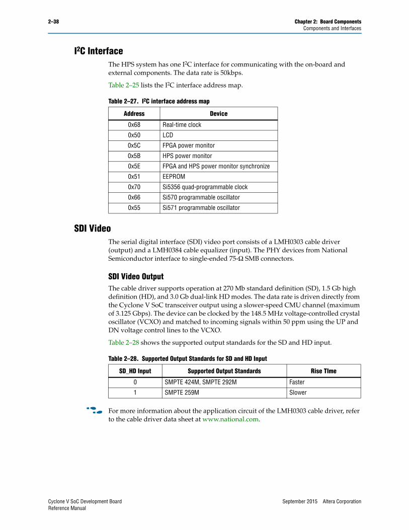
2–38 Chapter 2: Board ComponentsComponents and Interfaces
I2C InterfaceThe HPS system has one I2C interface for communicating with the on-board and external components. The data rate is 50kbps.
Table 2–25 lists the I2C interface address map.
SDI VideoThe serial digital interface (SDI) video port consists of a LMH0303 cable driver (output) and a LMH0384 cable equalizer (input). The PHY devices from National Semiconductor interface to single-ended 75-Ω SMB connectors.
SDI Video OutputThe cable driver supports operation at 270 Mb standard definition (SD), 1.5 Gb high definition (HD), and 3.0 Gb dual-link HD modes. The data rate is driven directly from the Cyclone V SoC transceiver output using a slower-speed CMU channel (maximum of 3.125 Gbps). The device can be clocked by the 148.5 MHz voltage-controlled crystal oscillator (VCXO) and matched to incoming signals within 50 ppm using the UP and DN voltage control lines to the VCXO.
Table 2–28 shows the supported output standards for the SD and HD input.
f For more information about the application circuit of the LMH0303 cable driver, refer to the cable driver data sheet at www.national.com.
Table 2–27. I2C interface address map
Address Device
0x68 Real-time clock
0x50 LCD
0x5C FPGA power monitor
0x5B HPS power monitor
0x5E FPGA and HPS power monitor synchronize
0x51 EEPROM
0x70 Si5356 quad-programmable clock
0x66 Si570 programmable oscillator
0x55 Si571 programmable oscillator
Table 2–28. Supported Output Standards for SD and HD Input
SD_HD Input Supported Output Standards Rise TIme
0 SMPTE 424M, SMPTE 292M Faster
1 SMPTE 259M Slower
Cyclone V SoC Development Board September 2015 Altera CorporationReference Manual

Chapter 2: Board Components 2–39Components and Interfaces
Table 2–29 summarizes the SDI video output interface pin assignments, signal names, and functions.
SDI Video InputThe cable equalizer supports operation at 270 Mb SD, 1.5 Gb HD, and 3.0 Gb dual-link HD modes. The data rate is driven directly from the Cyclone V SoC transceiver output using a slower-speed CMU channel (maximum of 3.125 Gbps). Control signals are allowed for bypassing or disabling the device, as well as a carrier detect or auto-mute signal interface.
Table 2–30 shows the cable equalizer lengths.
f For more information about the application circuit of the LMH0303 cable equalizer, refer to the cable equalizer data sheet at www.national.com.
Table 2–31 summarizes the SDI video input interface pin assignments, signal names, and functions.
Table 2–29. SDI Video Output Interface Pin Assignments, Schematic Signal Names, and Functions
Board Reference (U25) Schematic Signal Name I/O Standard Cyclone V SoC Device
Pin Number Description
6 SDI_TX_EN 2.5-V AA30 Device enable
4 SDI_TX_RSET 3.3-V — Device reset
10 SDI_TX_SD_HDn 2.5-V AC29 Slew rate control
1 SDI_TX_P 1.5-V PCML T4 SDI video input P
2 SDI_TX_N 1.5-V PCML T3 SDI video input N
Table 2–30. SDI Cable Equalizer Lengths
Data Rate (Mbps) Cable Type Maximum Cable Length (m)
270
Belden 1694A
400
1485 140
2970 120
Table 2–31. SDI Video Input Interface Pin Assignments, Schematic Signal Names, and Functions
Board Reference (U31) Schematic Signal Name I/O Standard Cyclone V SoC Device
Pin Number Description
7 SDI_RX_BYPASS 2.5-V AB28 Equalizer bypass enable
14 SDI_RX_EN 2.5-V AA28 Device enable
11 SDI_RX_P 1.5-V PCML U2 SDI video output P
10 SDI_RX_N 1.5-V PCML U1 SDI video output N
September 2015 Altera Corporation Cyclone V SoC Development BoardReference Manual

2–40 Chapter 2: Board ComponentsMemory
MemoryThis section describes the development board’s memory interface support and also their signal names, types, and connectivity relative to the Cyclone V SoC. The development board has the following memory interfaces:
■ DDR3 SDRAM (FPGA)
■ DDR3 SDRAM (HPS)
■ QSPI flash (HPS)
■ EPCQ flash
■ CFI flash
■ Micro SD flash memory
■ I2C EEPROM
f For more information about the memory interfaces, refer to the following documents:
■ Timing Analysis section in the External Memory Interface Handbook.
■ DDR, DDR2, and DDR3 SDRAM Design Tutorials section in the External Memory Interface Handbook.
DDR3 SDRAM (FPGA)The development board supports two 32Mx16x8 DDR3 SDRAM interface for very high-speed sequential memory access. The 32-bit data bus comprises of two ×16 devices with a single address or command bus. This interface connects to the dedicated HMC I/O banks on the bottom edge of the FPGA.
The DDR3 device shipped with this board are running at 400 MHz, for a total theoretical bandwidth of over 25.6 Gbps. The speed grade of this DDR3 device is 800 MHz with a CAS latency of 9.
Table 2–32 lists the DDR3 SDRAM pin assignments, signal names, and functions. The signal names and types are relative to the Cyclone V SoC in terms of I/O setting and direction.
Table 2–32. DDR3 SDRAM Pin Assignments, Schematic Signal Names, and Functions (Part 1 of 4)
Board Reference
SchematicSignal Name
Cyclone V SoC Pin Number I/O Standard Description
DDR3 x16 (U37)
N3 DDR3_FPGA_A0 AJ14 1.5-V SSTL Class I Address bus
P7 DDR3_FPGA_A1 AK14 1.5-V SSTL Class I Address bus
P3 DDR3_FPGA_A2 AH12 1.5-V SSTL Class I Address bus
N2 DDR3_FPGA_A3 AJ12 1.5-V SSTL Class I Address bus
P8 DDR3_FPGA_A4 AG15 1.5-V SSTL Class I Address bus
P2 DDR3_FPGA_A5 AH15 1.5-V SSTL Class I Address bus
R8 DDR3_FPGA_A6 AK12 1.5-V SSTL Class I Address bus
R2 DDR3_FPGA_A7 AK13 1.5-V SSTL Class I Address bus
Cyclone V SoC Development Board September 2015 Altera CorporationReference Manual

Chapter 2: Board Components 2–41Memory
T8 DDR3_FPGA_A8 AH13 1.5-V SSTL Class I Address bus
R3 DDR3_FPGA_A9 AH14 1.5-V SSTL Class I Address bus
L7 DDR3_FPGA_A10 AJ9 1.5-V SSTL Class I Address bus
R7 DDR3_FPGA_A11 AK9 1.5-V SSTL Class I Address bus
N7 DDR3_FPGA_A12 AK7 1.5-V SSTL Class I Address bus
T3 DDR3_FPGA_A13 AK8 1.5-V SSTL Class I Address bus
T7 DDR3_FPGA_A14 AG12 1.5-V SSTL Class I Address bus
M2 DDR3_FPGA_BA0 AH10 1.5-V SSTL Class I Bank address bus
N8 DDR3_FPGA_BA1 AJ11 1.5-V SSTL Class I Bank address bus
M3 DDR3_FPGA_BA2 AK11 1.5-V SSTL Class I Bank address bus
K3 DDR3_FPGA_CASN AH7 1.5-V SSTL Class I Row address select
K9 DDR3_FPGA_CKE AJ21 1.5-V SSTL Class I Column address select
J7 DDR3_FPGA_CLK_P AA14 Differential 1.5-V SSTL Class I Differential output clock
K7 DDR3_FPGA_CLK_N AA15 Differential 1.5-V SSTL Class I Differential output clock
L2 DDR3_FPGA_CSN AB15 1.5-V SSTL Class I Chip select
E7 DDR3_FPGA_DM2 AK23 1.5-V SSTL Class I Write mask byte lane
D3 DDR3_FPGA_DM3 AJ27 1.5-V SSTL Class I Write mask byte lane
E3 DDR3_FPGA_DQ16 AE19 1.5-V SSTL Class I Data bus
F2 DDR3_FPGA_DQ17 AE18 1.5-V SSTL Class I Data bus
H8 DDR3_FPGA_DQ18 AG22 1.5-V SSTL Class I Data bus
F8 DDR3_FPGA_DQ19 AK22 1.5-V SSTL Class I Data bus
H3 DDR3_FPGA_DQ20 AF21 1.5-V SSTL Class I Data bus
F7 DDR3_FPGA_DQ21 AF20 1.5-V SSTL Class I Data bus
G2 DDR3_FPGA_DQ22 AH23 1.5-V SSTL Class I Data bus
H7 DDR3_FPGA_DQ23 AK24 1.5-V SSTL Class I Data bus
D7 DDR3_FPGA_DQ24 AF24 1.5-V SSTL Class I Data bus
C8 DDR3_FPGA_DQ25 AF23 1.5-V SSTL Class I Data bus
C3 DDR3_FPGA_DQ26 AJ24 1.5-V SSTL Class I Data bus
C2 DDR3_FPGA_DQ27 AK26 1.5-V SSTL Class I Data bus
B8 DDR3_FPGA_DQ28 AE23 1.5-V SSTL Class I Data bus
A7 DDR3_FPGA_DQ29 AE22 1.5-V SSTL Class I Data bus
A2 DDR3_FPGA_DQ30 AG25 1.5-V SSTL Class I Data bus
A3 DDR3_FPGA_DQ31 AK27 1.5-V SSTL Class I Data bus
F3 DDR3_FPGA_DQS_P2 Y17 Differential 1.5-V SSTL Class I Data strobe P byte lane 2
G3 DDR3_FPGA_DQS_N2 AA18 Differential 1.5-V SSTL Class I Data strobe N byte lane 2
Table 2–32. DDR3 SDRAM Pin Assignments, Schematic Signal Names, and Functions (Part 2 of 4)
Board Reference
SchematicSignal Name
Cyclone V SoC Pin Number I/O Standard Description
September 2015 Altera Corporation Cyclone V SoC Development BoardReference Manual

2–42 Chapter 2: Board ComponentsMemory
C7 DDR3_FPGA_DQS_P3 AC20 Differential 1.5-V SSTL Class I Data strobe P byte lane 3
B7 DDR3_FPGA_DQS_N3 AD19 Differential 1.5-V SSTL Class I Data strobe N byte lane 3
K1 DDR3_FPGA_ODT AE16 1.5-V SSTL Class I On-die termination enable
J3 DDR3_FPGA_RASN AH8 1.5-V SSTL Class I Row address select
T2 DDR3_FPGA_RESETN AK21 1.5-V SSTL Class I Reset
L3 DDR3_FPGA_WEN AJ6 1.5-V SSTL Class I Write enable
L8 DDR3_FPGA_ZQ01 — 1.5-V SSTL Class I ZQ impedance calibration
DDR3 x16 (U38)
N3 DDR3_FPGA_A0 AJ14 1.5-V SSTL Class I Address bus
P7 DDR3_FPGA_A1 AK14 1.5-V SSTL Class I Address bus
P3 DDR3_FPGA_A2 AH12 1.5-V SSTL Class I Address bus
N2 DDR3_FPGA_A3 AJ12 1.5-V SSTL Class I Address bus
P8 DDR3_FPGA_A4 AG15 1.5-V SSTL Class I Address bus
P2 DDR3_FPGA_A5 AH15 1.5-V SSTL Class I Address bus
R8 DDR3_FPGA_A6 AK12 1.5-V SSTL Class I Address bus
R2 DDR3_FPGA_A7 AK13 1.5-V SSTL Class I Address bus
T8 DDR3_FPGA_A8 AH13 1.5-V SSTL Class I Address bus
R3 DDR3_FPGA_A9 AH14 1.5-V SSTL Class I Address bus
L7 DDR3_FPGA_A10 AJ9 1.5-V SSTL Class I Address bus
R7 DDR3_FPGA_A11 AK9 1.5-V SSTL Class I Address bus
N7 DDR3_FPGA_A12 AK7 1.5-V SSTL Class I Address bus
T3 DDR3_FPGA_A13 AK8 1.5-V SSTL Class I Address bus
T7 DDR3_FPGA_A14 AG12 1.5-V SSTL Class I Address bus
M2 DDR3_FPGA_BA0 AH10 1.5-V SSTL Class I Bank address bus
N8 DDR3_FPGA_BA1 AJ11 1.5-V SSTL Class I Bank address bus
M3 DDR3_FPGA_BA2 AK11 1.5-V SSTL Class I Bank address bus
K3 DDR3_FPGA_CASN AH7 1.5-V SSTL Class I Row address select
K9 DDR3_FPGA_CKE AJ21 1.5-V SSTL Class I Column address select
J7 DDR3_FPGA_CLK_P AA14 1.5-V SSTL Class I Differential output clock
K7 DDR3_FPGA_CLK_N AA15 1.5-V SSTL Class I Differential output clock
L2 DDR3_FPGA_CSN AB15 1.5-V SSTL Class I Chip select
E7 DDR3_FPGA_DM0 AH17 1.5-V SSTL Class I Write mask byte lane
D3 DDR3_FPGA_DM1 AG23 1.5-V SSTL Class I Write mask byte lane
E3 DDR3_FPGA_DQ0 AF18 1.5-V SSTL Class I Data bus
F2 DDR3_FPGA_DQ1 AE17 1.5-V SSTL Class I Data bus
H8 DDR3_FPGA_DQ2 AG16 1.5-V SSTL Class I Data bus
F8 DDR3_FPGA_DQ3 AF16 1.5-V SSTL Class I Data bus
Table 2–32. DDR3 SDRAM Pin Assignments, Schematic Signal Names, and Functions (Part 3 of 4)
Board Reference
SchematicSignal Name
Cyclone V SoC Pin Number I/O Standard Description
Cyclone V SoC Development Board September 2015 Altera CorporationReference Manual
Chapter 2: Board Components 2–43Memory
DDR3 SDRAM (HPS)The development board supports three 32Mx16x8 banks DDR3 SDRAM interface for very high-speed sequential memory access. The 40-bit data bus comprises of three ×16 devices with a single address or command bus. This interface connects to the dedicated HMC for HPS I/O banks on the top edge of the FPGA.
The DDR3 device shipped with this board are running at 400 MHz, for a total theoretical bandwidth of over 25.6 Gbps. The speed grade of this DDR3 device is 800 MHz with a CAS latency of 9.
H3 DDR3_FPGA_DQ4 AH20 1.5-V SSTL Class I Data bus
F7 DDR3_FPGA_DQ5 AG21 1.5-V SSTL Class I Data bus
G2 DDR3_FPGA_DQ6 AJ16 1.5-V SSTL Class I Data bus
H7 DDR3_FPGA_DQ7 AH18 1.5-V SSTL Class I Data bus
D7 DDR3_FPGA_DQ8 AK18 1.5-V SSTL Class I Data bus
C8 DDR3_FPGA_DQ9 AJ17 1.5-V SSTL Class I Data bus
C3 DDR3_FPGA_DQ10 AG18 1.5-V SSTL Class I Data bus
C2 DDR3_FPGA_DQ11 AK19 1.5-V SSTL Class I Data bus
B8 DDR3_FPGA_DQ12 AG20 1.5-V SSTL Class I Data bus
A7 DDR3_FPGA_DQ13 AF19 1.5-V SSTL Class I Data bus
A2 DDR3_FPGA_DQ14 AJ20 1.5-V SSTL Class I Data bus
A3 DDR3_FPGA_DQ15 AH24 1.5-V SSTL Class I Data bus
F3 DDR3_FPGA_DQS_P0 V16 Differential 1.5-V SSTL Class I Data strobe P byte lane 0
G3 DDR3_FPGA_DQS_N0 W16 Differential 1.5-V SSTL Class I Data strobe N byte lane 0
C7 DDR3_FPGA_DQS_P1 V17 Differential 1.5-V SSTL Class I Data strobe P byte lane 1
B7 DDR3_FPGA_DQS_N1 W17 Differential 1.5-V SSTL Class I Data strobe N byte lane 1
K1 DDR3_FPGA_ODT AE16 1.5-V SSTL Class I On-die termination enable
J3 DDR3_FPGA_RASN AH8 1.5-V SSTL Class I Row address select
T2 DDR3_FPGA_RESETN AK21 1.5-V SSTL Class I Reset
L3 DDR3_FPGA_WEN AJ6 1.5-V SSTL Class I Write enable
L8 DDR3_FPGA_ZQ01 — 1.5-V SSTL Class I ZQ impedance calibration
Table 2–32. DDR3 SDRAM Pin Assignments, Schematic Signal Names, and Functions (Part 4 of 4)
Board Reference
SchematicSignal Name
Cyclone V SoC Pin Number I/O Standard Description
September 2015 Altera Corporation Cyclone V SoC Development BoardReference Manual

2–44 Chapter 2: Board ComponentsMemory
Table 2–32 lists the DDR3 SDRAM pin assignments, signal names, and functions. The signal names and types are relative to the Cyclone V SoC in terms of I/O setting and direction.
Table 2–33. DDR3 SDRAM Pin Assignments, Schematic Signal Names, and Functions (Part 1 of 5)
Board Reference
SchematicSignal Name
Cyclone V SoC Pin Number I/O Standard Description
DDR3 x16 (U30)
N3 DDR3_HPS_A0 F26 1.5-V SSTL Class I Address bus
P7 DDR3_HPS_A1 G30 1.5-V SSTL Class I Address bus
P3 DDR3_HPS_A2 F28 1.5-V SSTL Class I Address bus
N2 DDR3_HPS_A3 F30 1.5-V SSTL Class I Address bus
P8 DDR3_HPS_A4 J25 1.5-V SSTL Class I Address bus
P2 DDR3_HPS_A5 J27 1.5-V SSTL Class I Address bus
R8 DDR3_HPS_A6 F29 1.5-V SSTL Class I Address bus
R2 DDR3_HPS_A7 E28 1.5-V SSTL Class I Address bus
T8 DDR3_HPS_A8 H27 1.5-V SSTL Class I Address bus
R3 DDR3_HPS_A9 G26 1.5-V SSTL Class I Address bus
L7 DDR3_HPS_A10 D29 1.5-V SSTL Class I Address bus
R7 DDR3_HPS_A11 C30 1.5-V SSTL Class I Address bus
N7 DDR3_HPS_A12 B30 1.5-V SSTL Class I Address bus
T3 DDR3_HPS_A13 C29 1.5-V SSTL Class I Address bus
T7 DDR3_HPS_A14 H25 1.5-V SSTL Class I Address bus
M2 DDR3_HPS_BA0 E29 1.5-V SSTL Class I Bank address bus
N8 DDR3_HPS_BA1 J24 1.5-V SSTL Class I Bank address bus
M3 DDR3_HPS_BA2 J23 1.5-V SSTL Class I Bank address bus
K3 DDR3_HPS_CASN E27 1.5-V SSTL Class I Row address select
K9 DDR3_HPS_CKE L29 1.5-V SSTL Class I Column address select
J7 DDR3_HPS_CLK_P L23 Differential 1.5-V SSTL Class I Differential output clock
K7 DDR3_HPS_CLK_N M23 Differential 1.5-V SSTL Class I Differential output clock
L2 DDR3_HPS_CSN H24 1.5-V SSTL Class I Chip select
E7 DDR3_HPS_DM4 W27 1.5-V SSTL Class I Write mask byte lane
F7 DDR3_HPS_DQ32 W26 1.5-V SSTL Class I Data bus
H7 DDR3_HPS_DQ33 R24 1.5-V SSTL Class I Data bus
F2 DDR3_HPS_DQ34 U27 1.5-V SSTL Class I Data bus
E3 DDR3_HPS_DQ35 V28 1.5-V SSTL Class I Data bus
H3 DDR3_HPS_DQ36 T25 1.5-V SSTL Class I Data bus
G2 DDR3_HPS_DQ37 U25 1.5-V SSTL Class I Data bus
H8 DDR3_HPS_DQ38 V27 1.5-V SSTL Class I Data bus
F8 DDR3_HPS_DQ39 Y29 1.5-V SSTL Class I Data bus
Cyclone V SoC Development Board September 2015 Altera CorporationReference Manual

Chapter 2: Board Components 2–45Memory
F3 DDR3_HPS_DQS_P4 T24 Differential 1.5-V SSTL Class I Data strobe P byte lane 4
G3 DDR3_HPS_DQS_N4 T23 Differential 1.5-V SSTL Class I Data strobe N byte lane 4
K1 DDR3_HPS_ODT H28 1.5-V SSTL Class I On-die termination enable
J3 DDR3_HPS_RASN D30 1.5-V SSTL Class I Row address select
T2 DDR3_HPS_RESETN P30 1.5-V SSTL Class I Reset
L3 DDR3_HPS_WEN C28 1.5-V SSTL Class I Write enable
L8 DDR3_HPS_ZQ01 — 1.5-V SSTL Class I ZQ impedance calibration
DDR3 x16 (U22)
N3 DDR3_HPS_A0 F26 1.5-V SSTL Class I Address bus
P7 DDR3_HPS_A1 G30 1.5-V SSTL Class I Address bus
P3 DDR3_HPS_A2 F28 1.5-V SSTL Class I Address bus
N2 DDR3_HPS_A3 F30 1.5-V SSTL Class I Address bus
P8 DDR3_HPS_A4 J25 1.5-V SSTL Class I Address bus
P2 DDR3_HPS_A5 J27 1.5-V SSTL Class I Address bus
R8 DDR3_HPS_A6 F29 1.5-V SSTL Class I Address bus
R2 DDR3_HPS_A7 E28 1.5-V SSTL Class I Address bus
T8 DDR3_HPS_A8 H27 1.5-V SSTL Class I Address bus
R3 DDR3_HPS_A9 G26 1.5-V SSTL Class I Address bus
L7 DDR3_HPS_A10 D29 1.5-V SSTL Class I Address bus
R7 DDR3_HPS_A11 C30 1.5-V SSTL Class I Address bus
N7 DDR3_HPS_A12 B30 1.5-V SSTL Class I Address bus
T3 DDR3_HPS_A13 C29 1.5-V SSTL Class I Address bus
T7 DDR3_HPS_A14 H25 1.5-V SSTL Class I Address bus
M2 DDR3_HPS_BA0 E29 1.5-V SSTL Class I Bank address bus
N8 DDR3_HPS_BA1 J24 1.5-V SSTL Class I Bank address bus
M3 DDR3_HPS_BA2 J23 1.5-V SSTL Class I Bank address bus
K3 DDR3_HPS_CASN E27 1.5-V SSTL Class I Row address select
K9 DDR3_HPS_CKE L29 1.5-V SSTL Class I Column address select
J7 DDR3_HPS_CLK_P L23 1.5-V SSTL Class I Differential output clock
K7 DDR3_HPS_CLK_N M23 1.5-V SSTL Class I Differential output clock
L2 DDR3_HPS_CSN H24 1.5-V SSTL Class I Chip select
E7 DDR3_HPS_DM2 R28 1.5-V SSTL Class I Write mask byte lane
D3 DDR3_HPS_DM3 W30 1.5-V SSTL Class I Write mask byte lane
H3 DDR3_HPS_DQ16 U26 1.5-V SSTL Class I Data bus
G2 DDR3_HPS_DQ17 T26 1.5-V SSTL Class I Data bus
H8 DDR3_HPS_DQ18 N29 1.5-V SSTL Class I Data bus
H7 DDR3_HPS_DQ19 N28 1.5-V SSTL Class I Data bus
Table 2–33. DDR3 SDRAM Pin Assignments, Schematic Signal Names, and Functions (Part 2 of 5)
Board Reference
SchematicSignal Name
Cyclone V SoC Pin Number I/O Standard Description
September 2015 Altera Corporation Cyclone V SoC Development BoardReference Manual

2–46 Chapter 2: Board ComponentsMemory
F2 DDR3_HPS_DQ20 P26 1.5-V SSTL Class I Data bus
E3 DDR3_HPS_DQ21 P27 1.5-V SSTL Class I Data bus
F8 DDR3_HPS_DQ22 N27 1.5-V SSTL Class I Data bus
F7 DDR3_HPS_DQ23 R29 1.5-V SSTL Class I Data bus
C8 DDR3_HPS_DQ24 P24 1.5-V SSTL Class I Data bus
B8 DDR3_HPS_DQ25 P25 1.5-V SSTL Class I Data bus
A3 DDR3_HPS_DQ26 T29 1.5-V SSTL Class I Data bus
C3 DDR3_HPS_DQ27 T28 1.5-V SSTL Class I Data bus
A7 DDR3_HPS_DQ28 R27 1.5-V SSTL Class I Data bus
D7 DDR3_HPS_DQ29 R26 1.5-V SSTL Class I Data bus
A2 DDR3_HPS_DQ30 V30 1.5-V SSTL Class I Data bus
C2 DDR3_HPS_DQ31 W29 1.5-V SSTL Class I Data bus
G3 DDR3_HPS_DQS_N2 R18 Differential 1.5-V SSTL Class I Data strobe P byte lane 0
B7 DDR3_HPS_DQS_N3 R21 Differential 1.5-V SSTL Class I Data strobe N byte lane 0
F3 DDR3_HPS_DQS_P2 R19 Differential 1.5-V SSTL Class I Data strobe P byte lane 1
C7 DDR3_HPS_DQS_P3 R22 Differential 1.5-V SSTL Class I Data strobe N byte lane 1
K1 DDR3_HPS_ODT H28 1.5-V SSTL Class I On-die termination enable
J3 DDR3_HPS_RASN D30 1.5-V SSTL Class I Row address select
T2 DDR3_HPS_RESETN P30 1.5-V SSTL Class I Reset
L3 DDR3_HPS_WEN C28 1.5-V SSTL Class I Write enable
L8 DDR3_HPS_ZQ2 — 1.5-V SSTL Class I ZQ impedance calibration
DDR3 x16 (U14)
N3 DDR3_HPS_A0 F26 1.5-V SSTL Class I Address bus
P7 DDR3_HPS_A1 G30 1.5-V SSTL Class I Address bus
P3 DDR3_HPS_A2 F28 1.5-V SSTL Class I Address bus
N2 DDR3_HPS_A3 F30 1.5-V SSTL Class I Address bus
P8 DDR3_HPS_A4 J25 1.5-V SSTL Class I Address bus
P2 DDR3_HPS_A5 J27 1.5-V SSTL Class I Address bus
R8 DDR3_HPS_A6 F29 1.5-V SSTL Class I Address bus
R2 DDR3_HPS_A7 E28 1.5-V SSTL Class I Address bus
T8 DDR3_HPS_A8 H27 1.5-V SSTL Class I Address bus
R3 DDR3_HPS_A9 G26 1.5-V SSTL Class I Address bus
L7 DDR3_HPS_A10 D29 1.5-V SSTL Class I Address bus
R7 DDR3_HPS_A11 C30 1.5-V SSTL Class I Address bus
N7 DDR3_HPS_A12 B30 1.5-V SSTL Class I Address bus
Table 2–33. DDR3 SDRAM Pin Assignments, Schematic Signal Names, and Functions (Part 3 of 5)
Board Reference
SchematicSignal Name
Cyclone V SoC Pin Number I/O Standard Description
Cyclone V SoC Development Board September 2015 Altera CorporationReference Manual

Chapter 2: Board Components 2–47Memory
T3 DDR3_HPS_A13 C29 1.5-V SSTL Class I Address bus
T7 DDR3_HPS_A14 H25 1.5-V SSTL Class I Address bus
M2 DDR3_HPS_BA0 E29 1.5-V SSTL Class I Bank address bus
N8 DDR3_HPS_BA1 J24 1.5-V SSTL Class I Bank address bus
M3 DDR3_HPS_BA2 J23 1.5-V SSTL Class I Bank address bus
K3 DDR3_HPS_CASN E27 1.5-V SSTL Class I Row address select
K9 DDR3_HPS_CKE L29 1.5-V SSTL Class I Column address select
J7 DDR3_HPS_CLK_P L23 1.5-V SSTL Class I Differential output clock
K7 DDR3_HPS_CLK_N M23 1.5-V SSTL Class I Differential output clock
L2 DDR3_HPS_CSN H24 1.5-V SSTL Class I Chip select
E7 DDR3_HPS_DM0 K28 1.5-V SSTL Class I Write mask byte lane
D3 DDR3_HPS_DM1 M28 1.5-V SSTL Class I Write mask byte lane
H8 DDR3_HPS_DQ0 K23 1.5-V SSTL Class I Data bus
H7 DDR3_HPS_DQ1 K22 1.5-V SSTL Class I Data bus
E3 DDR3_HPS_DQ2 H30 1.5-V SSTL Class I Data bus
H3 DDR3_HPS_DQ3 G28 1.5-V SSTL Class I Data bus
F7 DDR3_HPS_DQ4 L25 1.5-V SSTL Class I Data bus
F8 DDR3_HPS_DQ5 L24 1.5-V SSTL Class I Data bus
G2 DDR3_HPS_DQ6 J30 1.5-V SSTL Class I Data bus
F2 DDR3_HPS_DQ7 J29 1.5-V SSTL Class I Data bus
C8 DDR3_HPS_DQ8 K26 1.5-V SSTL Class I Data bus
B8 DDR3_HPS_DQ9 L26 1.5-V SSTL Class I Data bus
D7 DDR3_HPS_DQ10 K29 1.5-V SSTL Class I Data bus
A7 DDR3_HPS_DQ11 K27 1.5-V SSTL Class I Data bus
C2 DDR3_HPS_DQ12 M26 1.5-V SSTL Class I Data bus
C3 DDR3_HPS_DQ13 M27 1.5-V SSTL Class I Data bus
A3 DDR3_HPS_DQ14 L28 1.5-V SSTL Class I Data bus
A2 DDR3_HPS_DQ15 M30 1.5-V SSTL Class I Data bus
G3 DDR3_HPS_DQS_N0 M19 Differential 1.5-V SSTL Class I Data strobe P byte lane 0
B7 DDR3_HPS_DQS_N1 N24 Differential 1.5-V SSTL Class I Data strobe N byte lane 0
F3 DDR3_HPS_DQS_P0 N18 Differential 1.5-V SSTL Class I Data strobe P byte lane 1
C7 DDR3_HPS_DQS_P1 N25 Differential 1.5-V SSTL Class I Data strobe N byte lane 1
K1 DDR3_HPS_ODT H28 1.5-V SSTL Class I On-die termination enable
J3 DDR3_HPS_RASN D30 1.5-V SSTL Class I Row address select
T2 DDR3_HPS_RESETN P30 1.5-V SSTL Class I Reset
Table 2–33. DDR3 SDRAM Pin Assignments, Schematic Signal Names, and Functions (Part 4 of 5)
Board Reference
SchematicSignal Name
Cyclone V SoC Pin Number I/O Standard Description
September 2015 Altera Corporation Cyclone V SoC Development BoardReference Manual

2–48 Chapter 2: Board ComponentsMemory
QSPI Flash (HPS)The development board supports one 512-Mb quad-SPI (QSPI) flash device for non-volatile storage of the HPS boot code, user data, and program. The device connects to the HPS dedicated interface. The device interface may contain a secondary boot code.
This 4-bit data memory interface can sustain burst read operations at up to 108 MHz for a throughput of 54 MBps. Erase capability is at 4 KB, 64 KB, and 32 MB.
Table 2–34 lists the QSPI flash pin assignments, signal names, and functions. The signal names and types are relative to the Cyclone V SoC in terms of I/O setting and direction.
EPCQ FlashThe development board supports one 256-Mb serial/quad-serial NOR flash device for non-volatile storage of the FPGA configuration image. The device connects to the FPGA dedicated interface through the IDTQS3861 device.
Table 2–34 lists the EPCQ flash pin assignments, signal names, and functions. The signal names and types are relative to the MAX V CPLD 5M2210 System Controller in terms of I/O setting and direction. Some pins are used in other interfaces as well due to functionality sharing.
L3 DDR3_HPS_WEN C28 1.5-V SSTL Class I Write enable
L8 DDR3_HPS_ZQ — 1.5-V SSTL Class I ZQ impedance calibration
Table 2–33. DDR3 SDRAM Pin Assignments, Schematic Signal Names, and Functions (Part 5 of 5)
Board Reference
SchematicSignal Name
Cyclone V SoC Pin Number I/O Standard Description
Table 2–34. QSPI Flash Schematic Signal Names and Functions
Board Reference (U5)
SchematicSignal Name
Cyclone V SoC Pin Number I/O Standard Description
16 QSPI_CLK D19 3.3-V Clock
15 QSPI_IO0 C20 3.3-V Data bus
8 QSPI_IO1 H18 3.3-V Data bus
9 QSPI_IO2 A19 3.3-V Data bus
1 QSPI_IO3 E19 3.3-V Data bus
7 QSPI_SS0 A18 3.3-V Chip enable
3 QSPI_RESETN — 3.3-V Reset (driven from the MAX V CPLD)
Table 2–35. EPCQ Flash Schematic Signal Names and Functions
Board Reference (U20) Schematic Signal Name I/O Standard Description
16 FPGA_DCLK 3.3-V Clock
15 FPGA_AS_DATA0 3.3-V Data bus
8 FPGA_AS_DATA1 3.3-V Data bus
9 FPGA_AS_DATA2 3.3-V Data bus
Cyclone V SoC Development Board September 2015 Altera CorporationReference Manual
Chapter 2: Board Components 2–49Memory
CFI FlashThe development board supports a 512-Mb CFI-compatible synchronous flash device for non-volatile storage of FPGA configuration data. This device connects to the MAX V CPLD 5M2210 System Controller for FPGA configuration in FPP and PS modes.
This 16-bit data memory interface can sustain burst read operations at up to 52 MHz for a throughput of 832 Mbps per device. The write performance is 270 µs for a single word buffer while the erase time is 800 ms for a 128 K array block.
Table 2–36 lists the flash pin assignments, signal names, and functions. The signal names and types are relative to the MAX V CPLD 5M2210 System Controller in terms of I/O setting and direction.
1 FPGA_AS_DATA3 3.3-V Data bus
7 FPGA_NCS0 3.3-V Chip enable
Table 2–35. EPCQ Flash Schematic Signal Names and Functions
Board Reference (U20) Schematic Signal Name I/O Standard Description
Table 2–36. Flash Pin Assignments, Schematic Signal Names, and Functions (Part 1 of 2)
Board Reference (U6) Schematic Signal Name I/O Standard Description
F6 FLASH_ADVN 1.8-V Address valid
B4 FLASH_CEN0 1.8-V Chip enable
E6 FLASH_CLK 1.8-V Clock
F8 FLASH_OEN 1.8-V Output enable
F7 FLASH_RDYBSYN 1.8-V Ready
D4 FLASH_RESETN 1.8-V Reset
G8 FLASH_WEN 1.8-V Write enable
C6 FLASH_WPN 1.8-V Write protect
A1 FSM_A1 1.8-V Address bus
B1 FSM_A2 1.8-V Address bus
C1 FSM_A3 1.8-V Address bus
D1 FSM_A4 1.8-V Address bus
D2 FSM_A5 1.8-V Address bus
A2 FSM_A6 1.8-V Address bus
C2 FSM_A7 1.8-V Address bus
A3 FSM_A8 1.8-V Address bus
B3 FSM_A9 1.8-V Address bus
C3 FSM_A10 1.8-V Address bus
D3 FSM_A11 1.8-V Address bus
C4 FSM_A12 1.8-V Address bus
A5 FSM_A13 1.8-V Address bus
B5 FSM_A14 1.8-V Address bus
September 2015 Altera Corporation Cyclone V SoC Development BoardReference Manual

2–50 Chapter 2: Board ComponentsMemory
Micro SD Flash MemoryThe development board supports a micro SD card interface using x4 data lines. This dedicated HPS interface is the default location for storing HPS boot code, file system, and FPGA design binaries such as those found in the golden system reference design file. This 4-bit data interface can sustain burst read operations at up to 50 MHz for a throughput of 25 MBps.
C5 FSM_A15 1.8-V Address bus
D7 FSM_A16 1.8-V Address bus
D8 FSM_A17 1.8-V Address bus
A7 FSM_A18 1.8-V Address bus
B7 FSM_A19 1.8-V Address bus
C7 FSM_A20 1.8-V Address bus
C8 FSM_A21 1.8-V Address bus
A8 FSM_A22 1.8-V Address bus
G1 FSM_A23 1.8-V Address bus
H8 FSM_A24 1.8-V Address bus
B6 FSM_A25 1.8-V Address bus
B8 FSM_A26 1.8-V Address bus
F2 FSM_D0 1.8-V Data bus
E2 FSM_D1 1.8-V Data bus
G3 FSM_D2 1.8-V Data bus
E4 FSM_D3 1.8-V Data bus
E5 FSM_D4 1.8-V Data bus
G5 FSM_D5 1.8-V Data bus
G6 FSM_D6 1.8-V Data bus
H7 FSM_D7 1.8-V Data bus
E1 FSM_D8 1.8-V Data bus
E3 FSM_D9 1.8-V Data bus
F3 FSM_D10 1.8-V Data bus
F4 FSM_D11 1.8-V Data bus
F5 FSM_D12 1.8-V Data bus
H5 FSM_D13 1.8-V Data bus
G7 FSM_D14 1.8-V Data bus
E7 FSM_D15 1.8-V Data bus
Table 2–36. Flash Pin Assignments, Schematic Signal Names, and Functions (Part 2 of 2)
Board Reference (U6) Schematic Signal Name I/O Standard Description
Cyclone V SoC Development Board September 2015 Altera CorporationReference Manual
Chapter 2: Board Components 2–51Power Supply
Table 2–37 lists the micro SD flash memory interface pin assignments, signal names, and functions. The signal names and types are relative to the Cyclone V SoC in terms of I/O setting and direction.
I2C EEPROMThis board includes a 32 Kb EEPROM device. This device has a 2-wire I2C serial interface bus and is organized as four blocks of 4K x 8-bit memory. This device is programmed with special board information such as part number, test revision, and unique MAC addresses for all three Ethernet ports assigned to the board during manufacturing. This information can be displayed using the Board Test System's GUI as described in the development kit's user guide. This device can be accessed from the HPS, FPGA, or MAX V CPLD.
Table 2–38 lists the I2C EEPROM pin assignments, signal names, and functions. The signal names and types are relative to the Cyclone V SoC in terms of I/O setting and direction.
Power SupplyYou can power up the development board from a laptop-style DC power input or through the DC auxiliary connector. The Cyclone V SoC is designed in such way that the power rails for the HPS and FPGA are independent, allowing power down for the FPGA side using PM_CNTL0 when the HPS side is running. This eliminates power consumption on the FPGA part when not in use.
Table 2–37. Micro SD Flash Memory Interface Schematic Signal Names and Functions
Board Reference (J3)
Schematic Signal Name
Cyclone V SoC Pin Number I/O Standard Description
5 SD_CLK A16 3.3-V Clock
7 SD_DAT0 G18 3.3-V Data bus
8 SD_DAT1 C17 3.3-V Data bus
1 SD_DAT2 D17 3.3-V Data bus
2 SD_CD_DAT3 B16 3.3-V Control or data bus
3 SD_CMD F18 3.3-V Control
Table 2–38. I2C EEPROM Schematic Signal Names and Functions
Board Reference (U28)
Schematic Signal Name
Cyclone V SoC Pin Number I/O Standard Description
6 I2C_SCL_HPS D22 3.3-V HPS I2C serial clock
5 I2C_SDA_HPS C23 3.3-V HPS I2C serial data
September 2015 Altera Corporation Cyclone V SoC Development BoardReference Manual
2–52 Chapter 2: Board ComponentsPower Supply
Table 2–39 lists the maximum allowed draws of the power input.
An on-board multi-channel analog-to-digital converter (ADC) measures the current for several specific board rails.
Power Distribution SystemFigure 2–10 shows the power distribution system on the development board. Regulator inefficiencies and sharing are reflected in the currents shown, which are conservative absolute maximum levels.
Table 2–39. Power Input Maximum Allowed Draws
Source Voltage (V) Wattage (W)
Laptop Supply—DC input16.0 200
20.0 200
DC auxiliary connector 12.0 200
Cyclone V SoC Development Board September 2015 Altera CorporationReference Manual
Chapter 2: Board Components 2–53Power Supply
Figure 2–10. Power Distribution System
1.1V_HPS
C5SX HPS VCC
1.1 V, 1.923 AEN2342 (4 A)
Switching Regulator (+/- 2%)
0.24 A
1.5V_HPS
VCCIO HPS, VDD - DDR3
1.5 V, 3.194 AEN2342 (4 A)
Switching Regulator (+/- 2%)
0.459 A
3.3V_HPS
VCCPD, VCCIO, VDD ENET,
EZ-USB, VDD-USB2OTG,
VCC-RS232, VCC-CAN,
VDD-QSPI Flash, VCC/
Q-NAND Flash,
VCC-SDCARD, VCC-EPCQ
3.3 V, 3.005 AEN2342 (4 A)
Switching Regulator (+/- 2%)
0.897 A
2.5V_HPS
VCCPD, VCCIO, VCCRSTCLK,
VCCIO-MAXV, VCCIO-EPM570,
AVDD, VDD-ENET, Clocks
2.5 V,
2.826 AEN2342 (4 A)
Switching Regulator (+/- 2%)
0.67 A
2.5V_HPS_FILT
VCCPLL, VCCAUXBEAD
0.121 A
2.104 A
2.5V_VCCAUX_SHARED
HPS VCCAUX_SHAREDBEAD
0.038 A
1.2 V,
0.563 A
DVD_ENET
DVDD
LTC3022
1 A LDO
1.1V_VCC
C5SX FPGA VCC
1.1V_VCCEL
VCCE_GXB, VCCL_GXB
1.1 V,
11.316 A
BEAD
EN23F2 (15 A)
Switching Regulator (+/- 2%)
1.297 A
9.017 A
2.29 A
1.5V_FPGA
VCCIO, VDD - DDR3
1.5 V, 2.73 AEN2342 (4 A)
Switching Regulator (+/- 2%)
0.341 A
2.5V_FPGA
VCCPD, VCCPGM, VCCIO
2.5V_FPGA_FILT
VCCH_GXB, VCCA_FPLL,
VCCBAT
2.5 V,
3.606 A
BEAD
EN2342 (4 A)
Switching Regulator (+/- 2%)
0.84 A
1.281 A
2.325 A
5.0V
USB, LTCEXT
12V_EXP
HSMC, PCIe
3V3_EXP
HSMC, PCIe, ECAT-VDD
1V8
VCCINT/IO-MAXV, VCC-CFI
Flash, VCCINT-EMP570
LTC3509 Dual (0.7 A)
Switching Regulator (+/- 2%)
0.15 A
1.5 V, 0.6 A
1.8 V, 0.25 A
12 V, 6.5 A
3.3 V, 5.6 A
Ideal Diode
MultiplexerLTC3855 Dual
Channel
Controller
DC Input
19 V
DC AUX
12 V,
11.394 A
Ideal Diode
Multiplexer
Hot PlugController
September 2015 Altera Corporation Cyclone V SoC Development BoardReference Manual

2–54 Chapter 2: Board ComponentsPower Supply
Power MeasurementThere are seven power supply rails that have on-board current sense capabilities using 16-bit differential ADC devices. Precision sense resistors split the ADC devices and rails from the primary supply plane for the ADC to measure current. A SPI bus connects these ADC devices to the FPGA, HPS, and MAX V CPLD 5M2210 System Controller.
Figure 2–11 shows the block diagram for the power measurement circuitry.
Table 2–40 lists the targeted rails. The schematic signal name column specifies the name of the rail being measured while the device pin column specifies the devices attached to the rail.
Figure 2–11. Power Measurement Circuit
SCKSPI Bus
DSIDSOCSn
8 Ch.
Power Supply Load #0-6
R SENSE
MAX V CPLD5M2210System
Controller
Cyclone VSoC
To User PC
JTAG Chain
Feedback
14-pin2x16
CharacterLCD
ERWRSD(0:7)
Supply#0-6
EPM570 USBPHY
EmbeddedUSB-Blaster II
Table 2–40. Power Measurement Rails
Channel Schematic Signal Name Voltage (V) Device Pin Description
0 1.1V_HPS 1.1 VCC_HPS HPS core power
1 1.5V_HPS 1.5 VCCIO6A_HPS I/O and DDR3 devices
2 3.3V_HPS 3.3
VCCIO7A_HPS
I/O and HPS peripheral devicesVCCIO7B_HPS
VCCIO7C_HPS
VCCIO7D_HPS
3 2.5V_HPS 2.5 VCCPD6A6B_HPS I/O, HPS internal and peripheral devices
4 1.1V_VCC 1.1 VCC FPGA core power, transceiver, and clock
5 1.5V_FPGA 1.5VCCIO3B
I/O and DDR3 devicesVCCIO4A
6 2.5V_FPGA 2.5
VCCIO5A
I/O, FPGA internal and peripheral devices VCCIO5B
VCCIO8A
Cyclone V SoC Development Board September 2015 Altera CorporationReference Manual

September 2015 Altera Corporation
3. Board Components Reference
This chapter lists the component reference and manufacturing information of all the components on the Cyclone V SoC development board.
Table 3–1. Component Reference and Manufacturing Information
Board Reference Component Manufacturer Manufacturing
Part NumberManufacturer
Website
U21 Cyclone V SoC F896, 149,500 LEs, leadfree Altera Corporation 5CSXFC6D6F31C6 www.altera.com
U19 MAX V CPLD 5M2210 System Controller Altera Corporation 5M2210ZF256I5N www.altera.com
U51 High-Speed USB peripheral controller Cypress CY7C68013A www.cypress.com
U2 USB 2.0 On-the-go PHY device in 32QFN package with ULPI interface SMSC USB3300-EZK www.smsc.com
D1-D9, D14, D15, D17, D28-D31, D34, D37-D41
Green LEDs Lumex Inc. SML-LXT0805GW-TR www.lumex.com
D36 Red LED Lumex Inc. SML-LXT0805IW-TR www.lumex.com
D35 Blue LED Lumex Inc. SML-LX0805USBC-TR www.lumex.com
SW1–SW4 Four-position DIP switches C&K Components/ ITT Industries TDA04H0SB1 www.ittcannon.com
S1-S12 Push buttons Panasonic EVQPAC07K www.panasonic.com
J4 External Mictor 38-pin connector Tyco Electronics 2-767004-2 www.te.com
X1 Programmable LVDS clock 100M defaults Silicon Labs 570FAB000973DG www.silabs.com
X4 50 MHz crystal oscillator, ±50 ppm, CMOS, 2.5 V Silicon Labs 510GBA50M0000BAGx www.silabs.com
J12 Female angled PCB WR-DSUB 9-pin connector Wurth Elektronik 618009231121 www.we-online.com
J142×7 pin LCD socket strip Samtec TSM-107-07-G-D www.samtec.com
2×16 character LCD, 5×8 dot matrix Lumex Inc. LCM-S01602DSR/C www.lumex.com
U14, U15 Ethernet PHY BASE-T devices Marvell Semiconductor
88E1111-B2-CAA1C000 www.marvell.com
J2 MagJack 1000BaseT, 1×1 integrated connector module (ICM) Bel Fuse L829-1J1T-43 www.belfuse.com
J33, J34 RJ45 connector with integrated transformer Wurth Elektronik 7499011121A www.we-online.com
J25 PCIE socket ×4 Samtec PCIE-064-02-F-D-TH www.samtec.com
J12 HSMC, custom version of QSH-DP family high-speed socket Samtec ASP-122953-01 www.samtec.com
U25 3-Gbps HD/SD SDI cable driver National Semiconductor LMH0303SQ www.national.com
Cyclone V SoC Development BoardReference Manual
3–2 Chapter 3: Board Components Reference
U31 3-Gbps HD/SD SDI adaptive cable equalizer
National Semiconductor LMH0384SQ www.national.com
U50 3.3-V CAN transceiver with standby mode Texas Instruments SN65HVD230 www.ti.com
J35 Male angled PCB WR-DSUB 9-pin connector Wurth Elektronik 618-009-25023 www.we-online.com
U17 USB to serial UART interfaceFuture Technology
Devices International Ltd.
FT232RQ www.ftdichip.com
U3 Real-time clock Maxim DS1339C www.maxim-ic.com
J15, J16 2 x 8 debug headers Samtec TSM-108-01-L-DV www.samtec.com
U14, U22, U30, U37,
U38
32M × 16 × 8, 1024-MB DDR3 SDRAM Micron MT41K256M16HA-
125:E www.micron.com
U5 512-Mb QSPI flash Micron N25Q512A83GSF40F www.micron.com
U6 512-Mb CFI synchronous flash Numonyx PC28F512P30BFA www.numonyx.com
U20 256-Mb NOR flash Altera Corporation EPCQ256SI16N www.altera.com
U28 32-Kb EEPROM Microchip 24LC32A www.microchip.com
J3 Micro SD card socket Wurth Elektronik 693 071 010 811 www.we-online.com
U26, U34 Octal digital power supply manager with EEPROM Linear Technology LTC2978 www.linear.com
U7215 A voltage mode synchronous buck PWM DC-DC converter with integrated inductor
Enpirion EN23F2QI www.enpirion.com
U66, U67, U68, U69, U70, U71
4 A voltage mode synchronous buck PWM DC-DC converter with integrated inductor
Enpirion EN2340QI www.enpirion.com
Table 3–1. Component Reference and Manufacturing Information
Board Reference Component Manufacturer Manufacturing
Part NumberManufacturer
Website
Cyclone V SoC Development Board September 2015 Altera CorporationReference Manual

Chapter 3: Board Components Reference 3–3Statement of China-RoHS Compliance
Statement of China-RoHS ComplianceTable 3–2 lists hazardous substances included with the kit.
CE EMI Conformity CautionThis development kit is delivered conforming to relevant standards mandated by Directive 2004/108/EC. Because of the nature of programmable logic devices, it is possible for the user to modify the kit in such a way as to generate electromagnetic interference (EMI) that exceeds the limits established for this equipment. Any EMI caused as the result of modifications to the delivered material is the responsibility of the user.
Table 3–2. Table of Hazardous Substances’ Name and Concentration Notes (1), (2)
Part Name Lead (Pb)
Cadmium (Cd)
Hexavalent Chromium
(Cr6+)
Mercury (Hg)
Polybrominatedbiphenyls (PBB)
Polybrominateddiphenyl Ethers
(PBDE)
Cyclone V SoC development board X* 0 0 0 0 0
16 V power supply 0 0 0 0 0 0
Type A-B USB cable 0 0 0 0 0 0
User guide 0 0 0 0 0 0
Notes to Table 3–2:
(1) 0 indicates that the concentration of the hazardous substance in all homogeneous materials in the parts is below the relevant threshold of the SJ/T11363-2006 standard.
(2) X* indicates that the concentration of the hazardous substance of at least one of all homogeneous materials in the parts is above the relevant threshold of the SJ/T11363-2006 standard, but it is exempted by EU RoHS.
September 2015 Altera Corporation Cyclone V SoC Development BoardReference Manual

3–4 Chapter 3: Board Components ReferenceCE EMI Conformity Caution
Cyclone V SoC Development Board September 2015 Altera CorporationReference Manual

September 2015 Altera Corporation
Additional Information
This chapter provides additional information about the board, document and Altera.
Board Revision HistoryThe following table lists the versions of all releases of the Cyclone V SoC development board.
Document Revision HistoryThe following table lists the revision history for this document.
Release Date Version Description
September 2015 Production silicon Production silicon release and revision E PCB with Enperion EN23x2 power.
November 2013 Production silicon Production silicon release and revision D PCB with Enperion power.
May 2013 Engineering silicon Initial release for ES and revision C PCB.
Date Version Changes
September 2015 2.3
■ Correction to Table 2–23 on page 2–33: signal HSMA_TX_D_N14 is at pin C9
■ Corrections to Table 2–32 on page 2–40
■ Signal DDR3_FPGA_CLK_P is at pin AA14
■ Signal DDR3_FPGA_CLK_N is at pin AA15
■ Signal DDR3_FPGA_WEN is at pin AJ6
■ Correction to Figure 2–10 on page 2–53: hot plug controller is at input to LTC3855 Dual Channel Controller
August 2015 2.2
■ Corrections to Figure 1–1 on page 1–4:
■ USB 2.0 interface supported by MAX II device
■ No ECC on FPGA DDR3
■ Correction to “I/O Resources” on page 2–5: 181 general-purpose HPS I/O pins
■ Correction to “Power Distribution System” on page 2–53: switching regulator part number updated to EN23F2
■ Correction to Table 3–1 on page 3–1: switching regulator part number updated to EN23F2QI
■ Removed I/O count in “I/O Resources” and referred to Cyclone V Device Overview.
■ Updated “Power Distribution System” figure
■ Added “Mictor Jumper” section
■ Added ENET2_TX_CLK_FB to Table 2–22 on page 2–31
May 2014 2.1
■ Updated Figure 2–5, adding missing connections.
■ Updated Table 2–15, adding the X5 clock source.
■ Removed the term mini when referring to the USB port.
Cyclone V SoC Development BoardReference Manual

Info–2 Additional InformationAdditional InformationHow to Contact Altera
How to Contact AlteraTo locate the most up-to-date information about Altera products, refer to the following table.
Typographic ConventionsThe following table shows the typographic conventions this document uses.
November 2013 2.0
■ Revised the device part number to 5CSXFC6D6F31C6.
■ Changed the MAX V CPLD power sequence to 1.8 V.
■ Changed the QSPI device to N25Q512A83GSF40F.
■ Changed the Renesas PHY to uPD60620A.
■ Added Enpirion power component information.
■ Updated Figure 2–1.
■ Revised the FACTORY_LOAD switch description in Table 2–8.
■ Revised the HPS jumper description in Table 2–11.
August 2013 1.1 Revised the device part number.
May 2013 1.0 Initial release.
Date Version Changes
Contact (1) Contact Method Address
Technical support Website www.altera.com/support
Technical trainingWebsite www.altera.com/training
Email [email protected]
Product literature Website www.altera.com/literature
Nontechnical support (general) Email [email protected]
(software licensing) Email [email protected]
Note to Table:
(1) You can also contact your local Altera sales office or sales representative.
Visual Cue Meaning
Bold Type with Initial Capital Letters
Indicate command names, dialog box titles, dialog box options, and other GUI labels. For example, Save As dialog box. For GUI elements, capitalization matches the GUI.
bold typeIndicates directory names, project names, disk drive names, file names, file name extensions, software utility names, and GUI labels. For example, \qdesigns directory, D: drive, and chiptrip.gdf file.
Italic Type with Initial Capital Letters Indicate document titles. For example, Stratix IV Design Guidelines.
italic typeIndicates variables. For example, n + 1.
Variable names are enclosed in angle brackets (< >). For example, <file name> and <project name>.pof file.
Initial Capital Letters Indicate keyboard keys and menu names. For example, the Delete key and the Options menu.
Cyclone V SoC Development Board September 2015 Altera CorporationReference Manual

Additional InformationAdditional Information Info–3Typographic Conventions
“Subheading Title” Quotation marks indicate references to sections in a document and titles of Quartus II Help topics. For example, “Typographic Conventions.”
Courier type
Indicates signal, port, register, bit, block, and primitive names. For example, data1, tdi, and input. The suffix n denotes an active-low signal. For example, resetn.
Indicates command line commands and anything that must be typed exactly as it appears. For example, c:\qdesigns\tutorial\chiptrip.gdf.
Also indicates sections of an actual file, such as a Report File, references to parts of files (for example, the AHDL keyword SUBDESIGN), and logic function names (for example, TRI).
r An angled arrow instructs you to press the Enter key.
1., 2., 3., anda., b., c., and so on
Numbered steps indicate a list of items when the sequence of the items is important, such as the steps listed in a procedure.
■ ■ ■ Bullets indicate a list of items when the sequence of the items is not important.
1 The hand points to information that requires special attention.
h The question mark directs you to a software help system with related information.
f The feet direct you to another document or website with related information.
m The multimedia icon directs you to a related multimedia presentation.
c A caution calls attention to a condition or possible situation that can damage or destroy the product or your work.
w A warning calls attention to a condition or possible situation that can cause you injury.
The envelope links to the Email Subscription Management Center page of the Altera website, where you can sign up to receive update notifications for Altera documents.
The feedback icon allows you to submit feedback to Altera about the document. Methods for collecting feedback vary as appropriate for each document.
Visual Cue Meaning
September 2015 Altera Corporation Cyclone V SoC Development BoardReference Manual
Info–4 Additional InformationAdditional InformationTypographic Conventions
Cyclone V SoC Development Board September 2015 Altera CorporationReference Manual