Cyclone V E FPGA Development Kit User Guide - Altera · PDF fileCyclone V E FPGA Development...
38
101 Innovation Drive San Jose, CA 95134 www.altera.com UG-01129-1.2 User Guide Cyclone V E FPGA Development Kit Feedback Subscribe Cyclone V E FPGA Development Kit User Guide
Transcript of Cyclone V E FPGA Development Kit User Guide - Altera · PDF fileCyclone V E FPGA Development...
101 Innovation DriveSan Jose, CA 95134www.altera.com
UG-01129-1.2
User Guide
Cyclone V E FPGA Development Kit
Feedback Subscribe
Cyclone V E FPGA Development Kit User Guide

© 2014 Altera Corporation. All rights reserved. ALTERA, ARRIA, CYCLONE, HARDCOPY, MAX, MEGACORE, NIOS, QUARTUS and STRATIX words and logosare trademarks of Altera Corporation and registered in the U.S. Patent and Trademark Office and in other countries. All other words and logos identified astrademarks or service marks are the property of their respective holders as described at www.altera.com/common/legal.html. Altera warrants performance of itssemiconductor products to current specifications in accordance with Altera's standard warranty, but reserves the right to make changes to any products andservices at any time without notice. Altera assumes no responsibility or liability arising out of the application or use of any information, product, or servicedescribed herein except as expressly agreed to in writing by Altera. Altera customers are advised to obtain the latest version of device specifications before relyingon any published information and before placing orders for products or services.
December 2014 Altera Corporation Cyclone V E FPGA Development KitUser Guide
ISO 9001:2008 Registered

December 2014 Altera Corporation
Contents
Chapter 1. About This KitKit Features . . . . . . . . . . . . . . . . . . . . . . . . . . . . . . . . . . . . . . . . . . . . . . . . . . . . . . . . . . . . . . . . . . . . . . . . . . . . 1–1
Hardware . . . . . . . . . . . . . . . . . . . . . . . . . . . . . . . . . . . . . . . . . . . . . . . . . . . . . . . . . . . . . . . . . . . . . . . . . . . . 1–1Software . . . . . . . . . . . . . . . . . . . . . . . . . . . . . . . . . . . . . . . . . . . . . . . . . . . . . . . . . . . . . . . . . . . . . . . . . . . . . 1–1
Quartus II Web Edition Software . . . . . . . . . . . . . . . . . . . . . . . . . . . . . . . . . . . . . . . . . . . . . . . . . . . . . 1–1Cyclone V E FPGA Development Kit Installer . . . . . . . . . . . . . . . . . . . . . . . . . . . . . . . . . . . . . . . . . . 1–2
Chapter 2. Getting StartedBefore You Begin . . . . . . . . . . . . . . . . . . . . . . . . . . . . . . . . . . . . . . . . . . . . . . . . . . . . . . . . . . . . . . . . . . . . . . . . 2–1
Inspect the Board . . . . . . . . . . . . . . . . . . . . . . . . . . . . . . . . . . . . . . . . . . . . . . . . . . . . . . . . . . . . . . . . . . . . . 2–1References . . . . . . . . . . . . . . . . . . . . . . . . . . . . . . . . . . . . . . . . . . . . . . . . . . . . . . . . . . . . . . . . . . . . . . . . . . . . . . 2–2
Chapter 3. Software InstallationInstalling the Quartus II Web Edition Software . . . . . . . . . . . . . . . . . . . . . . . . . . . . . . . . . . . . . . . . . . . . . . 3–1
Licensing Considerations . . . . . . . . . . . . . . . . . . . . . . . . . . . . . . . . . . . . . . . . . . . . . . . . . . . . . . . . . . . . . . 3–1Installing the Development Kit . . . . . . . . . . . . . . . . . . . . . . . . . . . . . . . . . . . . . . . . . . . . . . . . . . . . . . . . . . . . 3–1Installing the USB-Blaster II Driver . . . . . . . . . . . . . . . . . . . . . . . . . . . . . . . . . . . . . . . . . . . . . . . . . . . . . . . . 3–2
Chapter 4. Development Board SetupSetting Up the Board . . . . . . . . . . . . . . . . . . . . . . . . . . . . . . . . . . . . . . . . . . . . . . . . . . . . . . . . . . . . . . . . . . . . . 4–1Factory Default Switch Settings . . . . . . . . . . . . . . . . . . . . . . . . . . . . . . . . . . . . . . . . . . . . . . . . . . . . . . . . . . . 4–2
Chapter 5. Board Update PortalConnecting to the Board Update Portal Web Page . . . . . . . . . . . . . . . . . . . . . . . . . . . . . . . . . . . . . . . . . . . 5–1Using the Board Update Portal to Update User Designs . . . . . . . . . . . . . . . . . . . . . . . . . . . . . . . . . . . . . . 5–2
Chapter 6. Board Test SystemPreparing the Board . . . . . . . . . . . . . . . . . . . . . . . . . . . . . . . . . . . . . . . . . . . . . . . . . . . . . . . . . . . . . . . . . . . . . 6–2Running the Board Test System . . . . . . . . . . . . . . . . . . . . . . . . . . . . . . . . . . . . . . . . . . . . . . . . . . . . . . . . . . . 6–2Using the Board Test System . . . . . . . . . . . . . . . . . . . . . . . . . . . . . . . . . . . . . . . . . . . . . . . . . . . . . . . . . . . . . . 6–3
The System Info Tab . . . . . . . . . . . . . . . . . . . . . . . . . . . . . . . . . . . . . . . . . . . . . . . . . . . . . . . . . . . . . . . . . . . 6–3Board Information . . . . . . . . . . . . . . . . . . . . . . . . . . . . . . . . . . . . . . . . . . . . . . . . . . . . . . . . . . . . . . . . . . 6–3MAX V Registers . . . . . . . . . . . . . . . . . . . . . . . . . . . . . . . . . . . . . . . . . . . . . . . . . . . . . . . . . . . . . . . . . . . 6–4JTAG Chain . . . . . . . . . . . . . . . . . . . . . . . . . . . . . . . . . . . . . . . . . . . . . . . . . . . . . . . . . . . . . . . . . . . . . . . . 6–4Qsys Memory Map . . . . . . . . . . . . . . . . . . . . . . . . . . . . . . . . . . . . . . . . . . . . . . . . . . . . . . . . . . . . . . . . . 6–5
The GPIO Tab . . . . . . . . . . . . . . . . . . . . . . . . . . . . . . . . . . . . . . . . . . . . . . . . . . . . . . . . . . . . . . . . . . . . . . . . 6–6Character LCD . . . . . . . . . . . . . . . . . . . . . . . . . . . . . . . . . . . . . . . . . . . . . . . . . . . . . . . . . . . . . . . . . . . . . 6–6User DIP Switches . . . . . . . . . . . . . . . . . . . . . . . . . . . . . . . . . . . . . . . . . . . . . . . . . . . . . . . . . . . . . . . . . . 6–6User LEDs . . . . . . . . . . . . . . . . . . . . . . . . . . . . . . . . . . . . . . . . . . . . . . . . . . . . . . . . . . . . . . . . . . . . . . . . . 6–7Push Button Switches . . . . . . . . . . . . . . . . . . . . . . . . . . . . . . . . . . . . . . . . . . . . . . . . . . . . . . . . . . . . . . . 6–7
The Flash Tab . . . . . . . . . . . . . . . . . . . . . . . . . . . . . . . . . . . . . . . . . . . . . . . . . . . . . . . . . . . . . . . . . . . . . . . . 6–7Read . . . . . . . . . . . . . . . . . . . . . . . . . . . . . . . . . . . . . . . . . . . . . . . . . . . . . . . . . . . . . . . . . . . . . . . . . . . . . . 6–8Write . . . . . . . . . . . . . . . . . . . . . . . . . . . . . . . . . . . . . . . . . . . . . . . . . . . . . . . . . . . . . . . . . . . . . . . . . . . . . 6–8Random Test . . . . . . . . . . . . . . . . . . . . . . . . . . . . . . . . . . . . . . . . . . . . . . . . . . . . . . . . . . . . . . . . . . . . . . . 6–8CFI Query . . . . . . . . . . . . . . . . . . . . . . . . . . . . . . . . . . . . . . . . . . . . . . . . . . . . . . . . . . . . . . . . . . . . . . . . . 6–8Increment Test . . . . . . . . . . . . . . . . . . . . . . . . . . . . . . . . . . . . . . . . . . . . . . . . . . . . . . . . . . . . . . . . . . . . . 6–8Reset . . . . . . . . . . . . . . . . . . . . . . . . . . . . . . . . . . . . . . . . . . . . . . . . . . . . . . . . . . . . . . . . . . . . . . . . . . . . . . 6–8Erase . . . . . . . . . . . . . . . . . . . . . . . . . . . . . . . . . . . . . . . . . . . . . . . . . . . . . . . . . . . . . . . . . . . . . . . . . . . . . . 6–8
Cyclone V E FPGA Development KitUser Guide

iv Contents
Data Display/Entry Boxes . . . . . . . . . . . . . . . . . . . . . . . . . . . . . . . . . . . . . . . . . . . . . . . . . . . . . . . . . . . 6–8Flash Memory Map . . . . . . . . . . . . . . . . . . . . . . . . . . . . . . . . . . . . . . . . . . . . . . . . . . . . . . . . . . . . . . . . . 6–8
The SSRAM Tab . . . . . . . . . . . . . . . . . . . . . . . . . . . . . . . . . . . . . . . . . . . . . . . . . . . . . . . . . . . . . . . . . . . . . . 6–9Read . . . . . . . . . . . . . . . . . . . . . . . . . . . . . . . . . . . . . . . . . . . . . . . . . . . . . . . . . . . . . . . . . . . . . . . . . . . . . . 6–9Write . . . . . . . . . . . . . . . . . . . . . . . . . . . . . . . . . . . . . . . . . . . . . . . . . . . . . . . . . . . . . . . . . . . . . . . . . . . . . 6–9Random Test . . . . . . . . . . . . . . . . . . . . . . . . . . . . . . . . . . . . . . . . . . . . . . . . . . . . . . . . . . . . . . . . . . . . . . 6–10Increment Test . . . . . . . . . . . . . . . . . . . . . . . . . . . . . . . . . . . . . . . . . . . . . . . . . . . . . . . . . . . . . . . . . . . . 6–10
The Power Monitor . . . . . . . . . . . . . . . . . . . . . . . . . . . . . . . . . . . . . . . . . . . . . . . . . . . . . . . . . . . . . . . . . . . . . 6–10General Information . . . . . . . . . . . . . . . . . . . . . . . . . . . . . . . . . . . . . . . . . . . . . . . . . . . . . . . . . . . . . . . 6–11Power Information . . . . . . . . . . . . . . . . . . . . . . . . . . . . . . . . . . . . . . . . . . . . . . . . . . . . . . . . . . . . . . . . . 6–11Power Graph . . . . . . . . . . . . . . . . . . . . . . . . . . . . . . . . . . . . . . . . . . . . . . . . . . . . . . . . . . . . . . . . . . . . . 6–11Graph Settings . . . . . . . . . . . . . . . . . . . . . . . . . . . . . . . . . . . . . . . . . . . . . . . . . . . . . . . . . . . . . . . . . . . . 6–11Reset . . . . . . . . . . . . . . . . . . . . . . . . . . . . . . . . . . . . . . . . . . . . . . . . . . . . . . . . . . . . . . . . . . . . . . . . . . . . . 6–11
The Clock Control . . . . . . . . . . . . . . . . . . . . . . . . . . . . . . . . . . . . . . . . . . . . . . . . . . . . . . . . . . . . . . . . . . . . . . 6–12Serial Port Registers . . . . . . . . . . . . . . . . . . . . . . . . . . . . . . . . . . . . . . . . . . . . . . . . . . . . . . . . . . . . . . . . 6–13fXTAL . . . . . . . . . . . . . . . . . . . . . . . . . . . . . . . . . . . . . . . . . . . . . . . . . . . . . . . . . . . . . . . . . . . . . . . . . . . 6–13Target Frequency . . . . . . . . . . . . . . . . . . . . . . . . . . . . . . . . . . . . . . . . . . . . . . . . . . . . . . . . . . . . . . . . . . 6–13Clear . . . . . . . . . . . . . . . . . . . . . . . . . . . . . . . . . . . . . . . . . . . . . . . . . . . . . . . . . . . . . . . . . . . . . . . . . . . . . 6–13Set New Frequency . . . . . . . . . . . . . . . . . . . . . . . . . . . . . . . . . . . . . . . . . . . . . . . . . . . . . . . . . . . . . . . . 6–13
Configuring the FPGA Using the Quartus II Programmer . . . . . . . . . . . . . . . . . . . . . . . . . . . . . . . . . . . . 6–13
Appendix A. Programming the Flash Memory DeviceCFI Flash Memory Map . . . . . . . . . . . . . . . . . . . . . . . . . . . . . . . . . . . . . . . . . . . . . . . . . . . . . . . . . . . . . . . . . A–1Preparing Design Files for Flash Programming . . . . . . . . . . . . . . . . . . . . . . . . . . . . . . . . . . . . . . . . . . . . . A–2
Creating Flash Files Using the Nios II EDS . . . . . . . . . . . . . . . . . . . . . . . . . . . . . . . . . . . . . . . . . . . . . . A–2Programming Flash Memory Using the Board Update Portal . . . . . . . . . . . . . . . . . . . . . . . . . . . . . . . . . A–2Programming Flash Memory Using the Nios II EDS . . . . . . . . . . . . . . . . . . . . . . . . . . . . . . . . . . . . . . . . . A–3Restoring the Flash Device to the Factory Settings . . . . . . . . . . . . . . . . . . . . . . . . . . . . . . . . . . . . . . . . . . A–4Restoring the MAX V CPLD to the Factory Settings . . . . . . . . . . . . . . . . . . . . . . . . . . . . . . . . . . . . . . . . . A–5
Additional InformationDocument Revision History . . . . . . . . . . . . . . . . . . . . . . . . . . . . . . . . . . . . . . . . . . . . . . . . . . . . . . . . . . . Info–1How to Contact Altera . . . . . . . . . . . . . . . . . . . . . . . . . . . . . . . . . . . . . . . . . . . . . . . . . . . . . . . . . . . . . . . . Info–1Typographic Conventions . . . . . . . . . . . . . . . . . . . . . . . . . . . . . . . . . . . . . . . . . . . . . . . . . . . . . . . . . . . . . Info–1
Cyclone V E FPGA Development Kit December 2014 Altera CorporationUser Guide

December 2014 Altera Corporation
1. About This Kit
The Altera® Cyclone® V E FPGA Development Kit is a complete design environment that includes both the hardware and software you need to develop Cyclone V E FPGA designs.
Kit FeaturesThis section briefly describes the Cyclone V E FPGA Development Kit contents.
f For a complete list of this kit’s contents and capabilities, refer to the Cyclone V E FPGA Development Kit page.
HardwareThe Cyclone V E FPGA Development Kit includes the following hardware:
■ Cyclone V E FPGA development board—A development platform that allows you to develop and prototype hardware designs running on the Cyclone V E FPGA.
f For detailed information about the board components and interfaces, refer to the Cyclone V E FPGA Development Board Reference Manual.
■ Debug Header Breakout Board HSMC.
■ Power supply and cables—The kit includes the following items:
■ Power supply and AC adapters for North America/Japan, Europe, and the United Kingdom.
■ USB cable.
■ Ethernet cable.
SoftwareThe software for this kit, described in the following sections, is available on the Altera website for immediate downloading. You can also request to have Altera mail the software to you on DVDs.
Quartus II Web Edition SoftwareThe Quartus II Web Edition Software is a licensed set of Altera tools with full functionality.
f Download the Quartus II Web Edition Software from the Quartus II Subscription Edition Software page of the Altera website. Alternatively, you can request a DVD from the Altera IP and Software DVD Request Form page of the Altera website.
Cyclone V E FPGA Development KitUser Guide
1–2 Chapter 1: About This KitKit Features
f To compare the Quartus II subscription and web editions, refer to Altera Quartus II Software — Subscription Edition vs. Web Edition. The kit also works in conjunction with the subscription edition.
Cyclone V E FPGA Development Kit InstallerThe license-free Cyclone V E FPGA Development Kit installer includes all the documentation and design examples for the kit.
For information on installing the Development Kit Installer, refer to “Installing the Development Kit” on page 3–1.
Cyclone V E FPGA Development Kit December 2014 Altera CorporationUser Guide
December 2014 Altera Corporation
2. Getting Started
The remaining chapters in this user guide lead you through the following Cyclone V E FPGA development board setup steps:
■ Inspecting the contents of the kit
■ Installing the design and kit software
■ Setting up, powering up, and verifying correct operation of the FPGA development board
■ Configuring the Cyclone V E FPGA
■ Running the Board Test System designs
f For complete information about the FPGA development board, refer to the Cyclone V E FPGA Development Board Reference Manual.
Before You BeginBefore using the kit or installing the software, check the kit contents and inspect the board to verify that you received all of the items listed in “Kit Features” on page 1–1. If any of the items are missing, contact Altera before you proceed.
Inspect the BoardPerform these steps:
1. Place the board on an anti-static surface and inspect it to ensure that it has not been damaged during shipment.
c Without proper anti-static handling, you can damage the board.
2. Verify that all components on the board appears in place and intact.
1 In typical applications with the Cyclone V E FPGA development board, a heat sink is not necessary. However, under extreme conditions, the board might require additional cooling to stay within operating temperature guidelines. The board has two holes near the FPGA that accommodate many different heat sinks, including the Dynatron V31G. You can perform power consumption and thermal modeling to determine whether your application requires additional cooling. For information about measuring board and FPGA power in real time, refer to “The Power Monitor” on page 6–10.
f For more information about power consumption and thermal modeling, refer to AN 358: Thermal Management for FPGAs.
Cyclone V E FPGA Development KitUser Guide

2–2 Chapter 2: Getting StartedReferences
ReferencesUse the following links to check the Altera website for other related information:
■ For the latest board design files and reference designs, refer to the Cyclone V E FPGA Development Kit page.
■ For additional daughter cards available for purchase, refer to the Development Board Daughtercards page.
■ For the Cyclone V E device documentation, refer to the Documentation: Cyclone V Devices page.
■ To purchase devices from the eStore, refer to the Devices page.
■ For Cyclone V E OrCAD symbols, refer to the Capture CIS Symbols page.
■ For Nios II 32-bit embedded processor solutions, refer to the Embedded Processing page.
Cyclone V E FPGA Development Kit December 2014 Altera CorporationUser Guide

December 2014 Altera Corporation
3. Software Installation
This chapter explains how to install the following software:
■ Quartus II Web Edition Software
■ Cyclone V E FPGA Development Kit software
■ On-Board USB-Blaster™ II driver
Installing the Quartus II Web Edition SoftwarePerform these steps:
1. Run the Quartus II Web Edition Software installer you acquired in “Software” on page 1–1.
2. Follow the on-screen instructions to complete the installation process, choosing an installation directory that is relative to the Quartus II software installation directory.
f For a list of the Web Edition capabilities and features, refer to the Detailed Comparison sheet.
f If you have difficulty installing the Quartus II software, refer to the Altera Software Installation and Licensing Manual.
Licensing ConsiderationsThe Quartus II Web Edition Software is license-free and supports Cyclone V E devices without any additional licensing requirement. This kit also works in conjunction with the Quartus II Subscription Edition Software, once you obtain the proper license file. To purchase a subscription, contact your Altera sales representative.
Installing the Development KitTo install the development kit, perform these steps:
1. Download the Cyclone V E FPGA Development Kit installer from the Cyclone V E FPGA Development Kit page of the Altera website. Alternatively, you can request a development kit DVD from the Altera Kit Installations DVD Request Form page of the Altera website.
2. Run the Cyclone V E FPGA Development Kit installer and follow the directions. Choose an installation directory that is relative to the Quartus II software installation directory.
Cyclone V E FPGA Development KitUser Guide
3–2 Chapter 3: Software InstallationInstalling the USB-Blaster II Driver
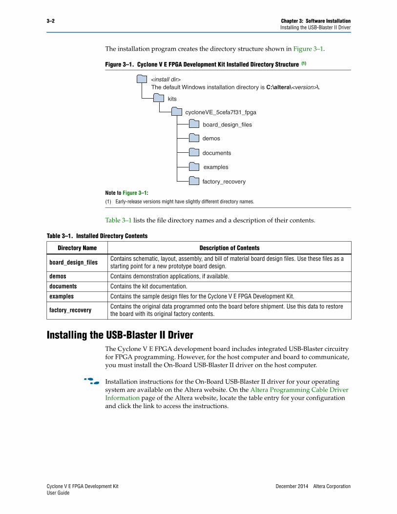
The installation program creates the directory structure shown in Figure 3–1.
Table 3–1 lists the file directory names and a description of their contents.
Installing the USB-Blaster II DriverThe Cyclone V E FPGA development board includes integrated USB-Blaster circuitry for FPGA programming. However, for the host computer and board to communicate, you must install the On-Board USB-Blaster II driver on the host computer.
f Installation instructions for the On-Board USB-Blaster II driver for your operating system are available on the Altera website. On the Altera Programming Cable Driver Information page of the Altera website, locate the table entry for your configuration and click the link to access the instructions.
Figure 3–1. Cyclone V E FPGA Development Kit Installed Directory Structure (1)
Note to Figure 3–1:
(1) Early-release versions might have slightly different directory names.
<install dir>
documents
board_design_files
The default Windows installation directory is C:\altera\<version>\.
examples
factory_recovery
demos
kits
cycloneVE_5cefa7f31_fpga
Table 3–1. Installed Directory Contents
Directory Name Description of Contents
board_design_files Contains schematic, layout, assembly, and bill of material board design files. Use these files as a starting point for a new prototype board design.
demos Contains demonstration applications, if available.
documents Contains the kit documentation.
examples Contains the sample design files for the Cyclone V E FPGA Development Kit.
factory_recovery Contains the original data programmed onto the board before shipment. Use this data to restore the board with its original factory contents.
Cyclone V E FPGA Development Kit December 2014 Altera CorporationUser Guide
December 2014 Altera Corporation
4. Development Board Setup
The instructions in this chapter explain how to set up the Cyclone V E FPGA development board.
Setting Up the BoardTo prepare and apply power to the board, perform these steps:
1. The FPGA development board ships with its board switches preconfigured to support the design examples in the kit. If you suspect your board might not be currently configured with the default settings, follow the instructions in “Factory Default Switch Settings” on page 4–2 to return the board to its factory settings before proceeding.
2. The FPGA development board ships with design examples stored in the flash memory device. Verify the DIP switch SW4.3 is set to the OFF (1) position to load the design stored in the factory portion of flash memory.
3. Connect the 65 W, 15 VDC @ 4.3 A power supply to the DC Power Jack (J17) on the FPGA board and plug the cord into a power outlet.
c Use only the supplied power supply. Power regulation circuitry on the board can be damaged by power supplies with greater voltage, and a lower-rated power supply may not be able to provide enough power for the board.
4. Set the POWER switch (SW5) to the on position. When power is supplied to the board, the blue LED (D35) illuminates indicating that the board has power.
The MAX V device on the board contains (among other things) a parallel flash loader (PFL) megafunction. When the board powers up, the PFL reads a design from flash memory and configures the FPGA. The DIP switch SW4.3 controls which design to load. When the switch is in the OFF (1) position, the PFL loads the design from the factory portion of flash memory.
1 The kit includes a MAX V design which contains the MAX V PFL megafunction. The design resides in the <install dir>\kits\cycloneVE_5cefa7f31_fpga\examples\max5 directory.
When configuration is complete, the Config Done LED (D19) illuminates, signaling that the Cyclone V E device configured successfully.
f For more information about the PFL megafunction, refer to the Parallel Flash Loader Megafunction User Guide.
Cyclone V E FPGA Development KitUser Guide
4–2 Chapter 4: Development Board SetupFactory Default Switch Settings
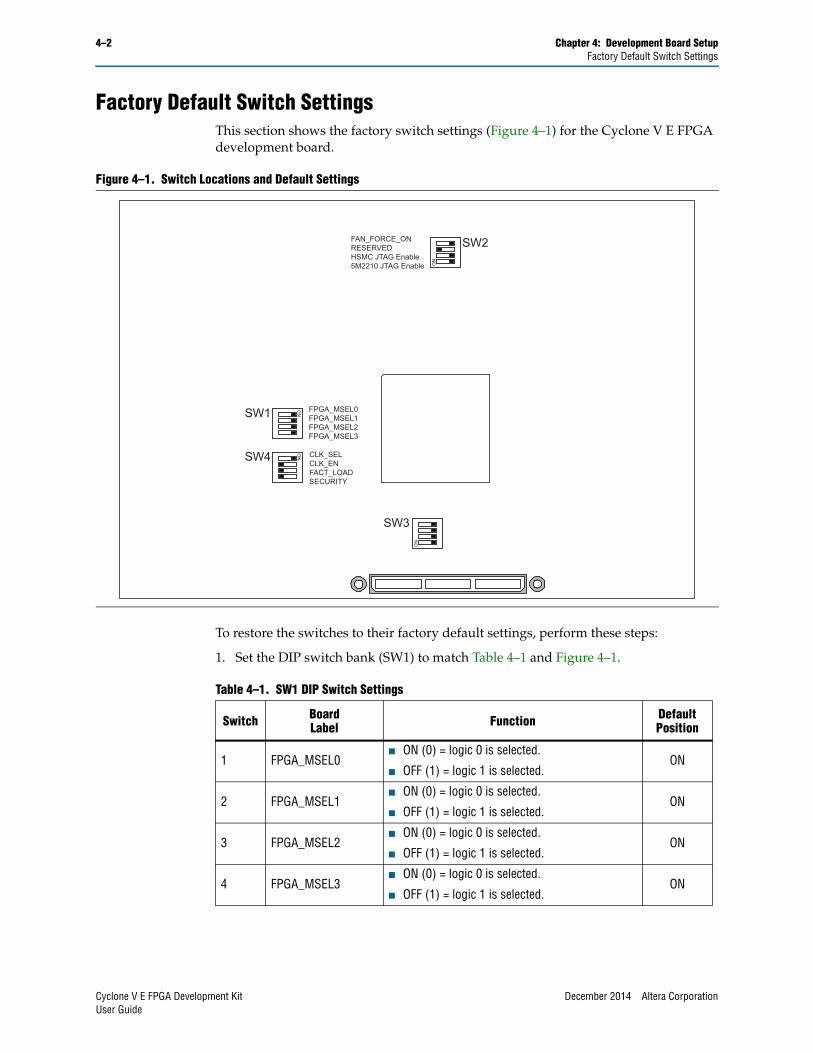
Factory Default Switch SettingsThis section shows the factory switch settings (Figure 4–1) for the Cyclone V E FPGA development board.
To restore the switches to their factory default settings, perform these steps:
1. Set the DIP switch bank (SW1) to match Table 4–1 and Figure 4–1.
Figure 4–1. Switch Locations and Default Settings
ONSW1
ONSW4
ON
SW3
ON
SW2
FPGA_MSEL0FPGA_MSEL1FPGA_MSEL2FPGA_MSEL3
FAN_FORCE_ONRESERVEDHSMC JTAG Enable5M2210 JTAG Enable
CLK_SELCLK_ENFACT_LOADSECURITY
Table 4–1. SW1 DIP Switch Settings
Switch BoardLabel Function Default
Position
1 FPGA_MSEL0■ ON (0) = logic 0 is selected.
■ OFF (1) = logic 1 is selected.ON
2 FPGA_MSEL1■ ON (0) = logic 0 is selected.
■ OFF (1) = logic 1 is selected.ON
3 FPGA_MSEL2■ ON (0) = logic 0 is selected.
■ OFF (1) = logic 1 is selected.ON
4 FPGA_MSEL3■ ON (0) = logic 0 is selected.
■ OFF (1) = logic 1 is selected.ON
Cyclone V E FPGA Development Kit December 2014 Altera CorporationUser Guide

Chapter 4: Development Board Setup 4–3Factory Default Switch Settings
2. Set the DIP switch bank (SW2) to match Table 4–2 and Figure 4–1.
3. Set the DIP switch bank (SW4) to match Table 4–3 and Figure 4–1.
f For more information about the FPGA board settings, refer to the Cyclone V E FPGA Development Board Reference Manual.
Table 4–2. SW2 JTAG DIP Switch Settings
Switch BoardLabel Function Default
Position
1 FAN_FORCE_ON■ ON (0) = Fan is turned on. (Fan not included.)
■ OFF (1) = Fan is turned off.OFF
2 RESERVED — —
3 HSMA_JTAG_EN
■ ON (0) = Do not Include the HSMC port in the JTAG chain.
■ OFF (1) = Include the HSMC port in the JTAG chain.
ON
4 5M2210_JTAG_EN
■ ON (0) = Do not Include MAX V system controller in the JTAG chain.
■ OFF (1) = Include MAX V system controller in the JTAG chain
OFF
Table 4–3. SW4 DIP Switch Settings
Switch BoardLabel Function Default
Position
1 CLK_SEL■ ON (0) = Select programmable oscillator clock.
■ OFF (1) = Select SMA input clock.ON
2 CLK_EN■ ON (0) = On-board oscillator is disabled.
■ OFF (1) = On-board oscillator is enabled.OFF
3 FACT_LOAD
■ ON (0) = Load the user design from flash at power up.
■ OFF (1) = Load the factory design from flash at power up.
OFF
4 SECURITY
■ ON (0) = Embedded On-Board USB Blaster II sends FACTORY command at power up.
■ OFF (1) = Embedded On-Board USB Blaster II does not send FACTORY command at power up.
OFF
December 2014 Altera Corporation Cyclone V E FPGA Development KitUser Guide
4–4 Chapter 4: Development Board SetupFactory Default Switch Settings
Cyclone V E FPGA Development Kit December 2014 Altera CorporationUser Guide
December 2014 Altera Corporation
5. Board Update Portal
The Cyclone V E FPGA Development Kit ships with the Board Update Portal design example stored in the factory portion of the flash memory on the board. The design consists of a Nios II embedded processor, an Ethernet MAC, and an HTML web server.
When you power up the board with the DIP switch SW4.3 in the OFF (1) position, the Cyclone V E FPGA configures with the Board Update Portal design example. The design can obtain an IP address from any DHCP server and serve a web page from the flash on your board to any host computer on the same network. The web page allows you to upload new FPGA designs to the user hardware 1 portion of flash memory and provides useful kit-specific links and design resources.
1 After successfully updating the user hardware 1 flash memory, you can load the user design from flash memory into the FPGA. To do so, set the DIP switch SW4.3 to the ON (0) position and power cycle the board.
The source code for the Board Update Portal design resides in the <install dir>\kits\cycloneVE_5cefa7f31_fpga\examples directory. If the Board Update Portal is corrupted or deleted from the flash memory, refer to “Restoring the Flash Device to the Factory Settings” on page A–4 to restore the board with its original factory contents.
Connecting to the Board Update Portal Web PageBefore you proceed, ensure that you have the following:
■ A PC with a connection to a working Ethernet port (J8) on a DHCP enabled network.
■ A separate working Ethernet port (J8) connected to the same network for the board.
■ The Ethernet and power cables that are included in the kit.
To connect to the Board Update Portal web page, perform these steps:
1. With the board powered down, set the DIP switch SW4.3 to the OFF (1) position.
2. Attach the Ethernet cable from the board to your LAN.
3. Power up the board. The board connects to the LAN’s gateway router and obtains an IP address. The LCD on the board displays the IP address.
4. Launch a web browser on a PC that is connected to the same network, and enter the IP address from the LCD into the browser address bar. The Board Update Portal web page appears in the browser.
1 You can click Cyclone V E FPGA Development Kit on the Board Update Portal web page to access the kit’s home page for documentation updates and additional new designs.
Cyclone V E FPGA Development KitUser Guide
5–2 Chapter 5: Board Update PortalUsing the Board Update Portal to Update User Designs
Using the Board Update Portal to Update User DesignsThe Board Update Portal allows you to write new designs to the user hardware 1 portion of flash memory. Designs must be in the Nios II Flash Programmer File (.flash) format.
1 Design files available from the Cyclone V E FPGA Development Kit page include .flash files. You can also create .flash files from your own custom design. Refer to “Preparing Design Files for Flash Programming” on page A–2 for information about preparing your own design for upload.
To upload a design over the network into the user portion of flash memory on your board, perform these steps:
1. Perform the steps in “Connecting to the Board Update Portal Web Page” to access the Board Update Portal web page.
2. In the Hardware File Name field, specify the .flash file that you either downloaded from the Altera website or created on your own. If there is a software component to the design, specify it in the same manner using the Software File Name field; otherwise, leave the Software File Name field blank.
3. Click Upload. The progress bar indicates the percent complete.
4. To configure the FPGA with the new design after the flash memory upload process is complete, set the DIP switch SW4.3 to the ON (0) position and power cycle the board.
1 As long as you don’t overwrite the factory image in the flash memory device, you can continue to use the Board Update Portal to write new designs to the user hardware 1 portion of flash memory. If you do overwrite the factory image, you can restore it by following the instructions in “Restoring the Flash Device to the Factory Settings” on page A–4.
Cyclone V E FPGA Development Kit December 2014 Altera CorporationUser Guide
December 2014 Altera Corporation
6. Board Test System
The kit includes an application called the Board Test System (BTS). The BTS provides an easy-to-use interface to alter functional settings and observe the results. You can use the BTS to test board components, modify functional parameters, observe performance, and measure power usage. While using the BTS, you reconfigure the FPGA several times with test designs specific to the functionality you are testing. (You can also use the BTS as a reference source for designing systems.)
To install the BTS, follow the steps in “Installing the Development Kit” on page 3–1.
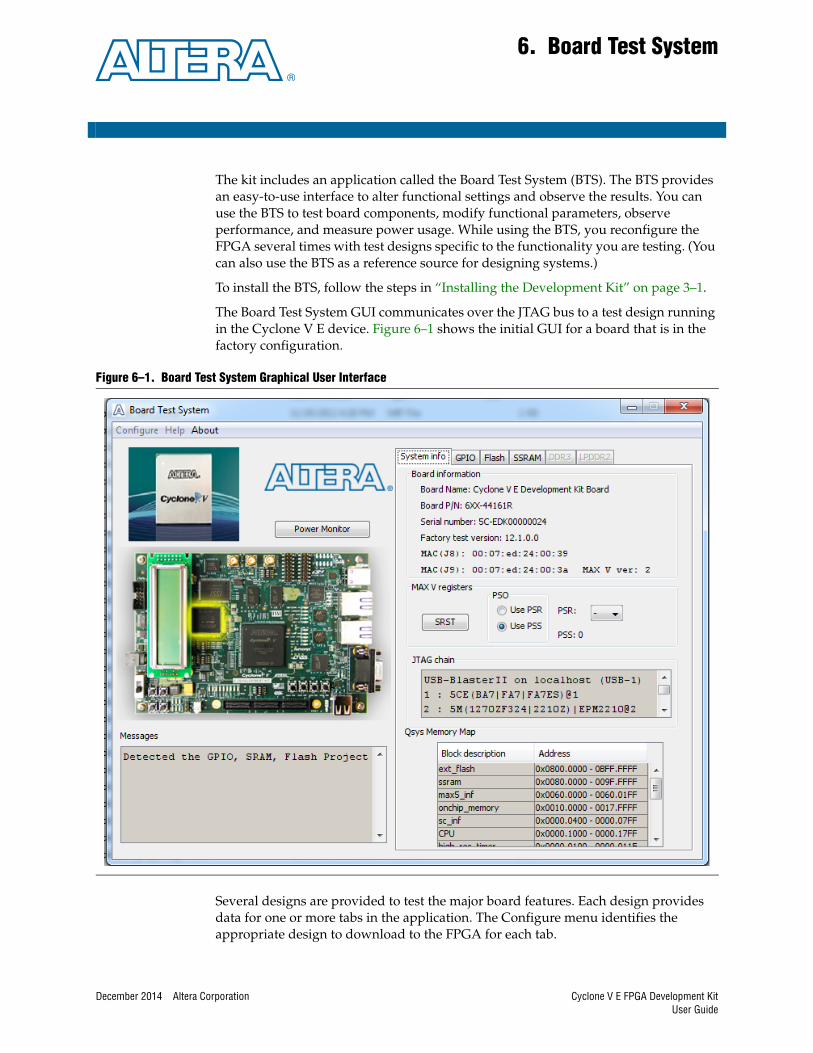
The Board Test System GUI communicates over the JTAG bus to a test design running in the Cyclone V E device. Figure 6–1 shows the initial GUI for a board that is in the factory configuration.
Several designs are provided to test the major board features. Each design provides data for one or more tabs in the application. The Configure menu identifies the appropriate design to download to the FPGA for each tab.
Figure 6–1. Board Test System Graphical User Interface
Cyclone V E FPGA Development KitUser Guide
6–2 Chapter 6: Board Test SystemPreparing the Board
After successful FPGA configuration, the appropriate tab appears and allows you to exercise the related board features. Highlights appear in the board picture around the corresponding components.
The Power Monitor button starts the Power Monitor application that measures and reports current power information for the board. Because the application communicates over the JTAG bus to the MAX V device, you can measure the power of any design in the FPGA, including your own designs.
1 The Board Test System and Power Monitor share the JTAG bus with other applications like the Nios II debugger and the SignalTap® II Embedded Logic Analyzer. Because the Quartus II programmer uses most of the bandwidth of the JTAG bus, other applications using the JTAG bus might time out. Be sure to close the other applications before attempting to reconfigure the FPGA using the Quartus II Programmer.
Preparing the BoardWith the power to the board off, follow these steps:
1. Connect the USB cable to the board.
2. Ensure that the Ethernet patch cord is plugged into the RJ45 connector (J8).
3. Ensure that the development board switches and jumpers are set to the default positions as shown in the “Factory Default Switch Settings” section starting on page 4–2.
4. Set the DIP switch SW4.3 to the ON (0) position.
f For more information about the board’s DIP switch and jumper settings, refer to the Cyclone V E FPGA Development Board Reference Manual.
5. Turn on the power to the board. The board loads the design stored in the user hardware 1 portion of flash memory into the FPGA. If your board is still in the factory configuration, or if you have downloaded a newer version of the Board Test System to flash memory through the Board Update Portal, the design loads the GPIO, SRAM, and flash memory tests.
c To ensure operating stability, keep the USB cable connected and the board powered on when running the demonstration application. The application cannot run correctly unless the USB cable is attached and the board is on.
Running the Board Test SystemTo run the application, navigate to the <install dir>\kits\cycloneVE_5cefa7f31_fpga\examples\board_test_system directory and run the BoardTestSystem.exe application.
1 On Windows, click Start > All Programs > Altera > Cyclone V E FPGA Development Kit <version> > Board Test System to run the application.
Cyclone V E FPGA Development Kit December 2014 Altera CorporationUser Guide
Chapter 6: Board Test System 6–3Using the Board Test System
A GUI appears, displaying the application tab that corresponds to the design running in the FPGA. The Cyclone V E FPGA development board’s flash memory ships preconfigured with the design that corresponds to the GPIO, Flash and SSRAM tabs.
1 If you power up your board with the DIP switch SW4.3 in a position other than the ON (0) position, or if you load your own design into the FPGA with the Quartus II Programmer, you receive a message prompting you to configure your board with a valid Board Test System design.
Using the Board Test SystemThis section describes each control in the Board Test System application.
The System Info TabThe System Info tab shows board’s current configuration. Figure 6–1 on page 6–1 shows the System Info tab. The tab displays the contents of the MAX V registers, the JTAG chain, the board’s MAC addresses, the flash memory map, and other details stored on the board.
The following sections describe the controls on the System Info tab.
Board InformationThe Board information controls display static information about your board.
■ Board Name—Indicates the official name of the board.
■ Part P/N—Indicates the part number of the board.
■ Serial number—Indicates the serial number of the board.
■ Factory test version—Indicates the version of the Board Test System currently running on the board.
■ MAC (J8)—Indicates the MAC addresses for Ethernet port (J8).
■ MAC (J9)—Indicates the MAC addresses for Ethernet port (J9).
■ MAX V ver—Indicates the version of MAX V code currently running on the board. The MAX V code resides in the <install dir>\kits\cycloneVE_5cefa7f31_fpga\examples directory. Newer revisions of this code might be available on the Cyclone V E FPGA Development Kit page of the Altera website.
December 2014 Altera Corporation Cyclone V E FPGA Development KitUser Guide
6–4 Chapter 6: Board Test SystemUsing the Board Test System
MAX V RegistersThe MAX V registers control allows you to view and change the current MAX V register values as described in Table 6–1. Changes to the register values with the GUI take effect immediately. For example, writing a 0 to SRST resets the board.
■ PSO—Sets the MAX V PSO register. The following options are available:
■ Use PSR—Allows the PSR to determine the page of flash memory to use for FPGA reconfiguration.
■ Use PSS—Allows the PSS to determine the page of flash memory to use for FPGA reconfiguration.
■ PSR—Sets the MAX V PSR register. The numerical values in the list corresponds to the page of flash memory to load during FPGA reconfiguration. Refer to Table 6–1 for more information.
■ PSS—Displays the MAX V PSS register value. Refer to Table 6–1 for the list of available options.
■ SRST—Resets the system and reloads the FPGA with a design from flash memory based on the other MAX V register values. Refer to Table 6–1 for more information.
1 Because the System Info tab requires that a specific design is running in the FPGA at a specific clock speed, writing a 0 to SRST or changing the PSO value can cause the Board Test System to stop running.
JTAG ChainThe JTAG chain control shows all the devices currently in the JTAG chain. The Cyclone V E device is always the first device in the chain. The JTAG chain is normally mastered by the On-board USB-Blaster II.
Table 6–1. MAX V Registers
Register Name Read/Write Capability Description
System Reset (SRST) Write only Set to 0 to initiate an FPGA reconfiguration.
Page Select Register (PSR) Read / Write
Determines which of the up to three (0-2) pages of flash memory to use for FPGA reconfiguration. The flash memory ships with pages 0 and 1 preconfigured.
Page Select Override (PSO) Read / Write
When set to 0, the value in PSR determines the page of flash memory to use for FPGA reconfiguration. When set to 1, the value in PSS determines the page of flash memory to use for FPGA reconfiguration.
Page Select Switch (PSS) Read only
Holds the current value of the illuminated PGM LED (D25-D27) based on the following encoding:
■ 0 = PGM LED (D25) and corresponds to the flash memory page for the factory hardware design
■ 1 = PGM LED (D26) and corresponds to the flash memory page for the user hardware 1 design
■ 2 = PGM LED (D27) and corresponds to the flash memory page for the user hardware 2 design
Cyclone V E FPGA Development Kit December 2014 Altera CorporationUser Guide
Chapter 6: Board Test System 6–5Using the Board Test System
1 If you plug in an external USB-Blaster cable to the JTAG header (J4), the On-Board USB-Blaster II is disabled.
1 JTAG DIP switch bank (SW2) selects which interfaces are in the chain. Refer to Table 4–2 on page 4–3 for detailed settings.
f For details on the JTAG chain, refer to the Cyclone V E FPGA Development Board Reference Manual. For USB-Blaster II configuration details, refer to the On-Board USB-Blaster II page.
Qsys Memory MapThe Qsys memory map control shows the memory map of the Qsys system on your board.
December 2014 Altera Corporation Cyclone V E FPGA Development KitUser Guide
6–6 Chapter 6: Board Test SystemUsing the Board Test System
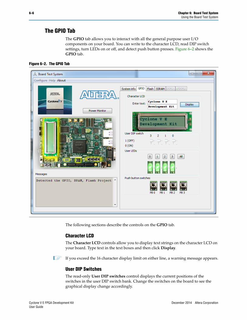
The GPIO TabThe GPIO tab allows you to interact with all the general purpose user I/O components on your board. You can write to the character LCD, read DIP switch settings, turn LEDs on or off, and detect push button presses. Figure 6–2 shows the GPIO tab.
The following sections describe the controls on the GPIO tab.
Character LCDThe Character LCD controls allow you to display text strings on the character LCD on your board. Type text in the text boxes and then click Display.
1 If you exceed the 16 character display limit on either line, a warning message appears.
User DIP SwitchesThe read-only User DIP switches control displays the current positions of the switches in the user DIP switch bank. Change the switches on the board to see the graphical display change accordingly.
Figure 6–2. The GPIO Tab
Cyclone V E FPGA Development Kit December 2014 Altera CorporationUser Guide
Chapter 6: Board Test System 6–7Using the Board Test System
User LEDsThe User LEDs control displays the current state of the user LEDs. Click the graphical representation of the LEDs to turn the board LEDs on and off. You can click ALL to turn on and off all of the user LEDs at once.
Push Button SwitchesThe read-only Push Button switches control displays the current state of the board user push buttons. Press a push button on the board to see the graphical display change accordingly.
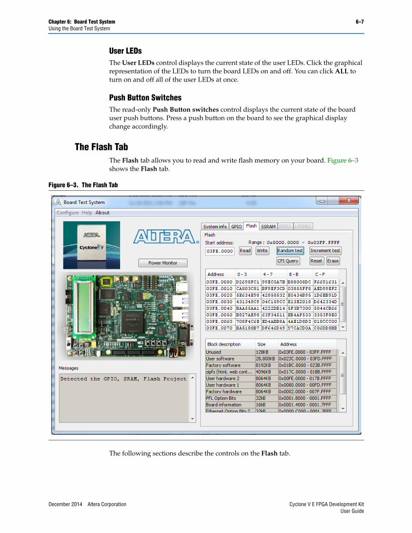
The Flash TabThe Flash tab allows you to read and write flash memory on your board. Figure 6–3 shows the Flash tab.
The following sections describe the controls on the Flash tab.
Figure 6–3. The Flash Tab
December 2014 Altera Corporation Cyclone V E FPGA Development KitUser Guide
6–8 Chapter 6: Board Test SystemUsing the Board Test System
ReadThe Read control reads the flash memory on your board. To see the flash memory contents, type a starting address in the text box and click Read. Values starting at the specified address appear in the table.
1 If you enter an address outside of the flash memory address space, a warning message identifies the valid flash memory address range.
WriteThe Write control writes the flash memory on your board. To update the flash memory contents, change values in the table and click Write. The application writes the new values to flash memory and then reads the values back to guarantee that the graphical display accurately reflects the memory contents.
Random TestStarts a random data pattern test to flash memory, which is limited to a scratch page in the upper 128K block.
CFI QueryThe CFI Query control updates the memory table, displaying the CFI ROM table contents from the flash device.
Increment TestStarts an incrementing data pattern test to flash memory, which is limited to a scratch page in the upper 128K block.
ResetThe Reset control executes the flash device’s reset command and updates the memory table displayed on the Flash tab.
EraseErases flash memory, which is limited to a scratch page in the upper 128K block.
Data Display/Entry BoxesThere are 8 rows and 4 columns. Each column contain 8 hexadecimal numbers. After entering the numbers in each cell, press Enter on your keyboard. Then click Write and Read button.
Flash Memory MapDisplays the flash memory map for the Cyclone V E FPGA Development Kit.
Cyclone V E FPGA Development Kit December 2014 Altera CorporationUser Guide
Chapter 6: Board Test System 6–9Using the Board Test System
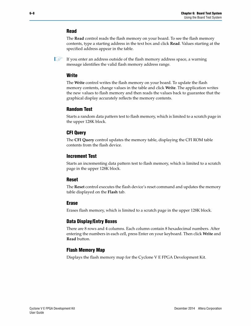
The SSRAM TabThe SSRAM tab allows you to read and write SRAM and flash memory on your board. Figure 6–4 shows the SSRAM tab.
The following sections describe the controls on the SSRAM tab.
ReadThe Read control reads the SRAM on your board. To see the SRAM contents, type a starting address in the text box and click Read. Values starting at the specified address appear in the table.
WriteThe Write control writes the SRAM on your board. To update the SRAM contents, change values in the table and click Write. The application writes the new values to SRAM and then reads the values back to guarantee that the graphical display accurately reflects the memory contents.
Figure 6–4. The SSRAM Tab
December 2014 Altera Corporation Cyclone V E FPGA Development KitUser Guide
6–10 Chapter 6: Board Test SystemThe Power Monitor
Random TestStarts a random data pattern test to SSRAM memory.
Increment TestStarts an incrementing data pattern test to SSRAM memory.
The Power MonitorThe Power Monitor measures and reports current power information. To start the application, click Power Monitor in the Board Test System application.
1 You can also run the Power Monitor as a stand-alone application. PowerMonitor.exe resides in the <install dir>\kits\cycloneVE_5cefa7f31_fpga\examples\board_test_system directory. On Windows, click Start > All Programs > Altera > Cyclone V E FPGA Development Kit <version> > Power Monitor to start the application.
The Power Monitor communicates with the MAX V device on the board through the JTAG bus. A power monitor circuit attached to the MAX V device allows you to measure the power that the Cyclone V E FPGA is consuming. Figure 6–5 shows the Power Monitor.
Figure 6–5. The Power Monitor
Cyclone V E FPGA Development Kit December 2014 Altera CorporationUser Guide
Chapter 6: Board Test System 6–11The Power Monitor
The following sections describe the Power Monitor controls.
General InformationThe General information controls display the following information about the MAX V device:
■ MAX V version—Indicates the version of MAX V code currently running on the board. The MAX V code resides in the <install dir>\kits\cycloneVE_5cefa7f31_fpga\factory_recovery and <install dir>\kits\cycloneVE_5cefa7f31_fpga\examples\max5 directories. Newer revisions of this code might be available on the Cyclone V E FPGA Development Kit page of the Altera website.
■ Power rail—Indicates the currently-selected power rail. After selecting the desired rail, click Reset to refresh the screen with new board readings.
f A table with the power rail information is available in the Cyclone V E FPGA Development Board Reference Manual.
Power InformationThe Power information control displays current, maximum, and minimum power readings for the following units:
■ mAmp
Power GraphThe power graph displays the mA power consumption of your board over time. The green line indicates the current value. The red line indicates the maximum value read since the last reset. The yellow line indicates the minimum value read since the last reset.
Graph SettingsThe following Graph settings controls allow you to define the look and feel of the power graph:
■ Scale select—Specifies the amount to scale the power graph. Select a smaller number to zoom in to see finer detail. Select a larger number to zoom out to see the entire range of recorded values.
■ Update speed—Specifies how often to refresh the graph.
ResetThis Reset control clears the graph, resets the minimum and maximum values, and restarts the Power Monitor.
December 2014 Altera Corporation Cyclone V E FPGA Development KitUser Guide

6–12 Chapter 6: Board Test SystemThe Clock Control
The Clock ControlThe Clock Control application sets the Si570 programmable oscillator to any frequency between 10 MHz and 810 MHz with eight digits of precision to the right of the decimal point. The default frequency for the oscillator is 125 MHz.
The Si570 device has one programmable output. The output of the Si570 drives a 1-to-4 clock fanout buffer that drives the top and bottom banks of the FPGA.
The Clock Control application runs as a stand-alone application. ClockControl.exe resides in the <install dir>\kits\cycloneVE_5cefa7f31_fpga\examples\board_test_system directory. On Windows, click Start > All Programs > Altera > Cyclone V E FPGA Development Kit <version> > Clock Control to start the application.
f For more information about the Si570 and the Cyclone V E FPGA development board’s clocking circuitry and clock input pins, refer to the Cyclone V E FPGA Development Board Reference Manual.
The Clock Control communicates with the MAX V device on the board through the JTAG bus. The Si570 programmable oscillator is connected to the MAX V device through a 2-wire serial bus. Figure 6–6 shows the Clock Control.
The following sections describe the Clock Control controls.
Figure 6–6. The Clock Control
Cyclone V E FPGA Development Kit December 2014 Altera CorporationUser Guide
Chapter 6: Board Test System 6–13Configuring the FPGA Using the Quartus II Programmer
Serial Port RegistersThe Serial port registers control shows the current values from the Si570 registers.
f For more information about the Si570 registers, refer to the Si570/Si571 data sheet available on the Silicon Labs website (www.silabs.com).
fXTALThe fXTAL control shows the calculated internal fixed-frequency crystal, based on the serial port register values.
For more information about the fXTAL value and how it is calculated, refer to the Si570/Si571 data sheet available on the Silicon Labs website (www.silabs.com).
Target FrequencyThe Target frequency control allows you to specify the frequency of the clock. Legal values are between 10 and 810 MHz with eight digits of precision to the right of the decimal point. For example, 421.31259873 is possible within 100 parts per million (ppm). The Target frequency control works in conjunction with the Set New Frequency control.
ClearThis control sets the frequency for the oscillator associated with the active tab back to its default value. This can also be accomplished by power cycling the board.
Set New FrequencyThe Set New Frequency control sets the programmable oscillator frequency for the selected clock to the value in the Target frequency control for the Si570. Frequency changes might take several milliseconds to take effect. You might see glitches on the clock during this time. Altera recommends resetting the FPGA logic after changing frequencies.
Configuring the FPGA Using the Quartus II ProgrammerYou can use the Quartus II Programmer to configure the FPGA with a specific .sof. Before configuring the FPGA, ensure the following:
■ The Quartus II Programmer and the USB-Blaster II driver are installed on the host computer.
■ The USB cable is connected to the FPGA development board.
■ Power to the board is on, and no other applications that use the JTAG chain are running.
To configure the Cyclone V E FPGA, perform these steps:
1. Start the Quartus II Programmer.
2. Click Auto Detect to display the devices in the JTAG chain.
3. Click Add File and select the path to the desired .sof.
4. Turn on the Program/Configure option for the added file.
December 2014 Altera Corporation Cyclone V E FPGA Development KitUser Guide

6–14 Chapter 6: Board Test SystemConfiguring the FPGA Using the Quartus II Programmer
5. Click Start to download the selected file to the FPGA. Configuration is complete when the progress bar reaches 100%.
1 Using the Quartus II programmer to configure a device on the board causes other JTAG-based applications such as the Board Test System and the Power Monitor to lose their connection to the board. Restart those applications after configuration is complete.
1 If the Quartus II programming window is already open, and then you power cycle the board, you may be required to click Hardware Setup in the Quartus II Programmer window and reselect USB-Blaster II in order to properly detect the JTAG chain.
Cyclone V E FPGA Development Kit December 2014 Altera CorporationUser Guide

December 2014 Altera Corporation
A. Programming the Flash MemoryDevice
As you develop your own project using the Altera tools, you can program the flash memory device so that your own design loads from flash memory into the FPGA on power up. This appendix describes the preprogrammed contents of the common flash interface (CFI) flash memory device on the Cyclone V E FPGA development board and the Nios II EDS tools involved with reprogramming the user portions of the flash memory device.
The Cyclone V E FPGA development board ships with the CFI flash device preprogrammed with a default factory FPGA configuration for running the Board Update Portal design example and a default user configuration for running the Board Test System demonstration. There are several other factory software files written to the CFI flash device to support the Board Update Portal. These software files were created using the Nios II EDS, just as the hardware design was created using the Quartus II software.
f For more information about Altera development tools, refer to the Design Software page of the Altera website.
CFI Flash Memory MapTable A–1 shows the default memory contents of the 512-Mb CFI flash device. For the Board Update Portal to run correctly and update designs in the user memory, this memory map must not be altered.
c Altera recommends that you do not overwrite the factory hardware and factory software images unless you are an expert with the Altera tools. If you unintentionally overwrite the factory hardware or factory software image, refer to “Restoring the Flash Device to the Factory Settings” on page A–4.
Table A–1. Byte Address Flash Memory Map
Block Description KB Size Address Range
Board Test System Scratch 128 0x03FE.0000 - 03FF.FFFF
User software 28,800 0x023C.0000 - 03FD.FFFF
Factory software 8192 0x01BC.0000 - 023B.FFFF
Zipfs (html, web content) 4096 0x017C.0000 - 01BB.FFFF
User hardware 2 8064 0x00FE.0000 - 017B.FFFF
User hardware 1 8064 0x0080.0000 - 00FD.FFFF
Factory hardware 8064 0x0002.0000 - 007F.FFFF
PFL option bits 32 0x0001.8000 - 0001.FFFF
Board information 16 0x0001.4000 - 0001.7FFF
Ethernet option bits 2 32 0x0000.C000 - 0001.3FFF
Ethernet option bits 1 32 0x0000.4000 - 0000.BFFF
User design reset vector 16 0x0000.0000 - 0000.3FFF
Cyclone V E FPGA Development KitUser Guide
A–2 Appendix A: Programming the Flash Memory DevicePreparing Design Files for Flash Programming
Preparing Design Files for Flash ProgrammingYou can obtain designs containing prepared .flash files from the Cyclone V E FPGA Development Kit page of the Altera website or create .flash files from your own custom design.
The Nios II EDS sof2flash command line utility converts your Quartus II-compiled .sof into the .flash format necessary for the flash device. Similarly, the Nios II EDS elf2flash command line utility converts your compiled and linked Executable and Linking Format File (.elf) software design to .flash. After your design files are in the .flash format, use the Board Update Portal or the Nios II EDS nios2-flash-programmer utility to write the .flash files to the user hardware 1 and user software locations of the flash memory.
f For more information about Nios II EDS software tools and practices, refer to the Embedded Software Development page of the Altera website.
Creating Flash Files Using the Nios II EDSIf you have an FPGA design developed using the Quartus II software, and software developed using the Nios II EDS, follow these instructions:
1. On the Windows Start menu, click All Programs > Altera > Nios II EDS > Nios II Command Shell.
2. In the Nios II command shell, navigate to the directory where your design files reside and type the following Nios II EDS commands:
■ For Quartus II .sof files:
sof2flash --input=<yourfile>_hw.sof --output=<yourfile>_hw.flash --offset=0x800000 --pfl --optionbit=0x00018000 --programmingmode=FPPr
■ For Nios II .elf files:
elf2flash --base=0x00000000 --end=0x03FFFFFF --reset=0x23C0000 --input=<yourfile>_sw.elf --output=<yourfile>_sw.flash --boot=$SOPC_KIT_NIOS2/components/altera_nios2/boot_loader_sources/boot_loader_cfi.srecr
The resulting .flash files are ready for flash device programming. If your design uses additional files such as image data or files used by the runtime program, you must first convert the files to .flash format and concatenate them into one .flash file before using the Board Update Portal to upload them.
1 The Board Update Portal standard .flash format conventionally uses either <filename>_hw.flash for hardware design files or <filename>_sw.flash for software design files.
Programming Flash Memory Using the Board Update PortalOnce you have the necessary .flash files, you can use the Board Update Portal to reprogram the flash memory. Refer to “Using the Board Update Portal to Update User Designs” on page 5–2 for more information.
Cyclone V E FPGA Development Kit December 2014 Altera CorporationUser Guide
Appendix A: Programming the Flash Memory Device A–3Programming Flash Memory Using the Nios II EDS
1 If you have generated a .sof that operates without a software design file, you can still use the Board Update Portal to upload your design. In this case, leave the Software File Name field blank.
Programming Flash Memory Using the Nios II EDSThe Nios II EDS offers a nios2-flash-programmer utility to program the flash memory directly. To program the .flash files or any compatible S-Record File (.srec) to the board using nios2-flash-programmer, perform these steps:
1. Set the DIP switch SW4.3 to the OFF (1) position to load the Board Update Portal design from flash memory on power up.
2. Attach the USB-Blaster cable and power up the board.
3. If the board has powered up and the LCD displays either Connecting... or a valid IP address (such as 152.198.231.75), proceed to step 8. If no output appears on the LCD or if the Config Done LED (D19) does not illuminate, continue to step 4 to load the FPGA with a flash-writing design.
4. Launch the Quartus II Programmer to configure the FPGA with a .sof capable of flash programming. Refer to “Configuring the FPGA Using the Quartus II Programmer” on page 6–13 for more information.
5. Click Add File and select <install dir>\kits\cycloneVE_5cefa7f31_fpga\factory_recovery\c5efa7_fpga_bup.sof.
6. Turn on the Program/Configure option for the added file.
7. Click Start to download the selected configuration file to the FPGA. Configuration is complete when the progress bar reaches 100%. The Config Done LED (D19) and the 4 User LEDs (D28-D31) illuminate indicating that the flash device is ready for programming.
8. On the Windows Start menu, click All Programs > Altera > Nios II EDS > Nios II Command Shell.
9. In the Nios II command shell, navigate to the <install dir>\kits\cycloneVE_5cefa7f31_fpga\factory_recovery directory (or to the directory of the .flash files you created in “Creating Flash Files Using the Nios II EDS” on page A–2) and type the following Nios II EDS command:
nios2-flash-programmer --base=0x00000000 <yourfile>_hw.flash r10. After programming completes, if you have a software file to program, type the
following Nios II EDS command:
nios2-flash-programmer --base=0x00000000 <yourfile>_sw.flash r11. Set the DIP switch SW4.3 to the ON (0) position and power cycle the board.
Programming the board is now complete.
f For more information about the nios2-flash-programmer utility, refer to the Nios II Flash Programmer User Guide.
December 2014 Altera Corporation Cyclone V E FPGA Development KitUser Guide
A–4 Appendix A: Programming the Flash Memory DeviceRestoring the Flash Device to the Factory Settings
Restoring the Flash Device to the Factory SettingsThis section describes how to restore the original factory contents to the flash memory device on the FPGA development board. Make sure you have the Nios II EDS installed, and perform these steps:
1. Set the board switches to the factory default settings described in “Factory Default Switch Settings” on page 4–2.
2. Launch the Quartus II Programmer to configure the FPGA with a .sof capable of flash programming. Refer to “Configuring the FPGA Using the Quartus II Programmer” on page 6–13 for more information.
3. Click Add File and select <install dir>\kits\cycloneVE_5cefa7f31_fpga\factory_recovery\c5efa7_fpga_bup.sof.
4. Turn on the Program/Configure option for the added file.
5. Click Start to download the selected configuration file to the FPGA. Configuration is complete when the progress bar reaches 100%. The Config Done LED (D19) and the 4 User LEDs (D28-D31) illuminate indicating that the flash device is ready for programming. The flash device is ready for programming.
6. On the Windows Start menu, click All Programs > Altera > Nios II EDS > Nios II Command Shell.
7. In the Nios II command shell, navigate to the <install dir>\kits\cycloneVE_5cefa7f31_fpga\factory_recovery directory and type the following command to run the restore script:
./restore.sh rRestoring the flash memory might take several minutes. Follow any instructions that appear in the Nios II command shell.
8. After all flash programming completes, cycle the POWER switch (SW5) off then on.
9. Using the Quartus II Programmer, click Add File and select <install dir>\kits\cycloneVE_5cefa7f31_fpga\factory_recovery\c5efa7_fpga_bup.sof.
10. Turn on the Program/Configure option for the added file.
11. Click Start to download the selected configuration file to the FPGA. Configuration is complete when the progress bar reaches 100%. The Config Done LED (D19) and the 4 User LEDs (D28-D31) illuminate indicating the flash memory device is now restored with the factory contents. The flash device is ready for programming.
12. After all flash programming completes, cycle the POWER switch (SW5) off then on.
13. The restore script cannot restore the board’s MAC address automatically. In the Nios II command shell, type the following Nios II EDS command:
nios2-terminal rand follow the instructions in the terminal window to generate unique MAC addresses for two Ethernet ports.
Cyclone V E FPGA Development Kit December 2014 Altera CorporationUser Guide
Appendix A: Programming the Flash Memory Device A–5Restoring the MAX V CPLD to the Factory Settings
f To ensure that you have the most up-to-date factory restore files and information about this product, refer to the Cyclone V E FPGA Development Kit page of the Altera website.
Restoring the MAX V CPLD to the Factory SettingsThis section describes how to restore the original factory contents to the MAX V CPLD on the FPGA development board. Make sure you have the Nios II EDS installed, and perform these steps:
1. Set the board switches to the factory default settings described in “Factory Default Switch Settings” on page 4–2.
1 DIP switch SW2.1 includes the MAX V device in the JTAG chain.
2. Launch the Quartus II Programmer.
3. Click Auto Detect.
4. Click Add File and select <install dir>\kits\cycloneVE_5cefa7f31_fpga\factory_recovery\max5.pof.
5. Turn on the Program/Configure option for the added file.
6. Click Start to download the selected configuration file to the MAX V CPLD. Configuration is complete when the progress bar reaches 100%.
f To ensure that you have the most up-to-date factory restore files and information about this product, refer to the Cyclone V E FPGA Development Kit page of the Altera website.
December 2014 Altera Corporation Cyclone V E FPGA Development KitUser Guide
A–6 Appendix A: Programming the Flash Memory DeviceRestoring the MAX V CPLD to the Factory Settings
Cyclone V E FPGA Development Kit December 2014 Altera CorporationUser Guide
December 2014 Altera Corporation
Additional Information
This chapter provides additional information about the document and Altera.
Document Revision HistoryThe following table shows the revision history for this document.
How to Contact AlteraTo locate the most up-to-date information about Altera products, refer to the following table.
Typographic ConventionsThe following table shows the typographic conventions this document uses.
Date Version Changes
December 2014 1.2 Corrections to the Switch Locations and Default Settings drawing in chapter 4.
March 2013 1.1
Updates for change from engineering sample silicon to production silicon.
Updates to BTS screenshots.
Additions for CE compliance.
November 2012 1.0 Initial release.
Contact (1) Contact Method Address
Technical support Website www.altera.com/support
Technical trainingWebsite www.altera.com/training
Email [email protected]
Product literature Website www.altera.com/literature
Nontechnical support (general) Email [email protected]
(software licensing) Email [email protected]
Note to Table:
(1) You can also contact your local Altera sales office or sales representative.
Visual Cue Meaning
Bold Type with Initial Capital Letters
Indicate command names, dialog box titles, dialog box options, and other GUI labels. For example, Save As dialog box. For GUI elements, capitalization matches the GUI.
bold typeIndicates directory names, project names, disk drive names, file names, file name extensions, software utility names, and GUI labels. For example, \qdesigns directory, D: drive, and chiptrip.gdf file.
Italic Type with Initial Capital Letters Indicate document titles. For example, Stratix IV Design Guidelines.
Cyclone V E FPGA Development KitUser Guide
Info–2 Additional InformationTypographic Conventions
c Electromagnetic interference caused by modification of the kit contents is the sole responsibility of the user.
This equipment is designated for use only in an industrial research environment.
italic typeIndicates variables. For example, n + 1.
Variable names are enclosed in angle brackets (< >). For example, <file name> and <project name>.pof file.
Initial Capital Letters Indicate keyboard keys and menu names. For example, the Delete key and the Options menu.
“Subheading Title” Quotation marks indicate references to sections in a document and titles of Quartus II Help topics. For example, “Typographic Conventions.”
Courier type
Indicates signal, port, register, bit, block, and primitive names. For example, data1, tdi, and input. The suffix n denotes an active-low signal. For example, resetn.
Indicates command line commands and anything that must be typed exactly as it appears. For example, c:\qdesigns\tutorial\chiptrip.gdf.
Also indicates sections of an actual file, such as a Report File, references to parts of files (for example, the AHDL keyword SUBDESIGN), and logic function names (for example, TRI).
r An angled arrow instructs you to press the Enter key.
1., 2., 3., anda., b., c., and so on
Numbered steps indicate a list of items when the sequence of the items is important, such as the steps listed in a procedure.
■ ■ ■ Bullets indicate a list of items when the sequence of the items is not important.
1 The hand points to information that requires special attention.
h The question mark directs you to a software help system with related information.
f The feet direct you to another document or website with related information.
m The multimedia icon directs you to a related multimedia presentation.
c A caution calls attention to a condition or possible situation that can damage or destroy the product or your work.
w A warning calls attention to a condition or possible situation that can cause you injury.
The envelope links to the Email Subscription Management Center page of the Altera website, where you can sign up to receive update notifications for Altera documents.
The feedback icon allows you to submit feedback to Altera about the document. Methods for collecting feedback vary as appropriate for each document.
Visual Cue Meaning
Cyclone V E FPGA Development Kit December 2014 Altera CorporationUser Guide