Cyclone III FPGA Development Kit User Guide - Altera · Cyclone III FPGA Development Kit User Guide...
48
101 Innovation Drive San Jose, CA 95134 www.altera.com UG-01027-1.4 P25-36208-03 User Guide Cyclone III FPGA Development Kit Subscribe Cyclone III FPGA Development Kit User Guide
Transcript of Cyclone III FPGA Development Kit User Guide - Altera · Cyclone III FPGA Development Kit User Guide...
101 Innovation DriveSan Jose, CA 95134www.altera.com
UG-01027-1.4P25-36208-03
User Guide
Cyclone III FPGA Development Kit
Subscribe
Cyclone III FPGA Development Kit User Guide

Cyclone III FPGA Development Kit User Guide September 2010 Altera Corporation
© 2010 Altera Corporation. All rights reserved. ALTERA, ARRIA, CYCLONE, HARDCOPY, MAX, MEGACORE, NIOS, QUARTUS and STRATIX are Reg. U.S. Pat.& Tm. Off. and/or trademarks of Altera Corporation in the U.S. and other countries. All other trademarks and service marks are the property of their respectiveholders as described at www.altera.com/common/legal.html. Altera warrants performance of its semiconductor products to current specifications in accordancewith Altera’s standard warranty, but reserves the right to make changes to any products and services at any time without notice. Altera assumes no responsibility orliability arising out of the application or use of any information, product, or service described herein except as expressly agreed to in writing by Altera. Alteracustomers are advised to obtain the latest version of device specifications before relying on any published information and before placing orders for products orservices.
September 2010 Altera Corporation
Contents
Chapter 1. About This KitIntroduction . . . . . . . . . . . . . . . . . . . . . . . . . . . . . . . . . . . . . . . . . . . . . . . . . . . . . . . . . . . . . . . . . . . . . . . . . . . . 1–1Kit Features . . . . . . . . . . . . . . . . . . . . . . . . . . . . . . . . . . . . . . . . . . . . . . . . . . . . . . . . . . . . . . . . . . . . . . . . . . . . 1–1Documentation . . . . . . . . . . . . . . . . . . . . . . . . . . . . . . . . . . . . . . . . . . . . . . . . . . . . . . . . . . . . . . . . . . . . . . . . . 1–2
Chapter 2. Getting StartedIntroduction . . . . . . . . . . . . . . . . . . . . . . . . . . . . . . . . . . . . . . . . . . . . . . . . . . . . . . . . . . . . . . . . . . . . . . . . . . . . 2–1Before You Begin . . . . . . . . . . . . . . . . . . . . . . . . . . . . . . . . . . . . . . . . . . . . . . . . . . . . . . . . . . . . . . . . . . . . . . . . 2–1
Check the Kit Contents . . . . . . . . . . . . . . . . . . . . . . . . . . . . . . . . . . . . . . . . . . . . . . . . . . . . . . . . . . . . . . . . 2–1Inspect the Board . . . . . . . . . . . . . . . . . . . . . . . . . . . . . . . . . . . . . . . . . . . . . . . . . . . . . . . . . . . . . . . . . . . . . 2–2Hardware Requirements . . . . . . . . . . . . . . . . . . . . . . . . . . . . . . . . . . . . . . . . . . . . . . . . . . . . . . . . . . . . . . . 2–2Software Requirements . . . . . . . . . . . . . . . . . . . . . . . . . . . . . . . . . . . . . . . . . . . . . . . . . . . . . . . . . . . . . . . . 2–2
References . . . . . . . . . . . . . . . . . . . . . . . . . . . . . . . . . . . . . . . . . . . . . . . . . . . . . . . . . . . . . . . . . . . . . . . . . . . . . . 2–3
Chapter 3. Software InstallationIntroduction . . . . . . . . . . . . . . . . . . . . . . . . . . . . . . . . . . . . . . . . . . . . . . . . . . . . . . . . . . . . . . . . . . . . . . . . . . . . 3–1Installing the Cyclone III Development Kit . . . . . . . . . . . . . . . . . . . . . . . . . . . . . . . . . . . . . . . . . . . . . . . . . . 3–1Installing the Quartus II Web Edition Software . . . . . . . . . . . . . . . . . . . . . . . . . . . . . . . . . . . . . . . . . . . . . . 3–2
Licensing Considerations . . . . . . . . . . . . . . . . . . . . . . . . . . . . . . . . . . . . . . . . . . . . . . . . . . . . . . . . . . . . . . 3–3Installing the USB-Blaster Driver . . . . . . . . . . . . . . . . . . . . . . . . . . . . . . . . . . . . . . . . . . . . . . . . . . . . . . . . . . 3–3
Chapter 4. Development Board SetupIntroduction . . . . . . . . . . . . . . . . . . . . . . . . . . . . . . . . . . . . . . . . . . . . . . . . . . . . . . . . . . . . . . . . . . . . . . . . . . . . 4–1Requirements . . . . . . . . . . . . . . . . . . . . . . . . . . . . . . . . . . . . . . . . . . . . . . . . . . . . . . . . . . . . . . . . . . . . . . . . . . . 4–1Powering Up the Board . . . . . . . . . . . . . . . . . . . . . . . . . . . . . . . . . . . . . . . . . . . . . . . . . . . . . . . . . . . . . . . . . . 4–2Configuring the FPGA . . . . . . . . . . . . . . . . . . . . . . . . . . . . . . . . . . . . . . . . . . . . . . . . . . . . . . . . . . . . . . . . . . . 4–4
Chapter 5. Board Update PortalIntroduction . . . . . . . . . . . . . . . . . . . . . . . . . . . . . . . . . . . . . . . . . . . . . . . . . . . . . . . . . . . . . . . . . . . . . . . . . . . . 5–1Connecting to the Board Update Portal Web Page . . . . . . . . . . . . . . . . . . . . . . . . . . . . . . . . . . . . . . . . . . . 5–1Using the Board Update Portal to Update User Designs . . . . . . . . . . . . . . . . . . . . . . . . . . . . . . . . . . . . . . 5–2
Chapter 6. Board Test SystemIntroduction . . . . . . . . . . . . . . . . . . . . . . . . . . . . . . . . . . . . . . . . . . . . . . . . . . . . . . . . . . . . . . . . . . . . . . . . . . . . 6–1Preparing the Board . . . . . . . . . . . . . . . . . . . . . . . . . . . . . . . . . . . . . . . . . . . . . . . . . . . . . . . . . . . . . . . . . . . . . 6–2Running the Board Test System . . . . . . . . . . . . . . . . . . . . . . . . . . . . . . . . . . . . . . . . . . . . . . . . . . . . . . . . . . . 6–3Using the Board Test System . . . . . . . . . . . . . . . . . . . . . . . . . . . . . . . . . . . . . . . . . . . . . . . . . . . . . . . . . . . . . . 6–4
The Configure Menu . . . . . . . . . . . . . . . . . . . . . . . . . . . . . . . . . . . . . . . . . . . . . . . . . . . . . . . . . . . . . . . . . . 6–4The Config Tab . . . . . . . . . . . . . . . . . . . . . . . . . . . . . . . . . . . . . . . . . . . . . . . . . . . . . . . . . . . . . . . . . . . . . . . 6–4
MAX II Registers . . . . . . . . . . . . . . . . . . . . . . . . . . . . . . . . . . . . . . . . . . . . . . . . . . . . . . . . . . . . . . . . . . . 6–4JTAG Chain . . . . . . . . . . . . . . . . . . . . . . . . . . . . . . . . . . . . . . . . . . . . . . . . . . . . . . . . . . . . . . . . . . . . . . . . 6–4Board Information . . . . . . . . . . . . . . . . . . . . . . . . . . . . . . . . . . . . . . . . . . . . . . . . . . . . . . . . . . . . . . . . . . 6–5Flash Memory Map . . . . . . . . . . . . . . . . . . . . . . . . . . . . . . . . . . . . . . . . . . . . . . . . . . . . . . . . . . . . . . . . . 6–5
The GPIO Tab . . . . . . . . . . . . . . . . . . . . . . . . . . . . . . . . . . . . . . . . . . . . . . . . . . . . . . . . . . . . . . . . . . . . . . . . 6–5Character LCD . . . . . . . . . . . . . . . . . . . . . . . . . . . . . . . . . . . . . . . . . . . . . . . . . . . . . . . . . . . . . . . . . . . . . 6–6User DIP Switches . . . . . . . . . . . . . . . . . . . . . . . . . . . . . . . . . . . . . . . . . . . . . . . . . . . . . . . . . . . . . . . . . . 6–6User LEDs . . . . . . . . . . . . . . . . . . . . . . . . . . . . . . . . . . . . . . . . . . . . . . . . . . . . . . . . . . . . . . . . . . . . . . . . . 6–6Push Button Switches . . . . . . . . . . . . . . . . . . . . . . . . . . . . . . . . . . . . . . . . . . . . . . . . . . . . . . . . . . . . . . . 6–6
Cyclone III FPGA Development Kit User Guide
iv Contents
7-Segment Display . . . . . . . . . . . . . . . . . . . . . . . . . . . . . . . . . . . . . . . . . . . . . . . . . . . . . . . . . . . . . . . . . . 6–6Ethernet . . . . . . . . . . . . . . . . . . . . . . . . . . . . . . . . . . . . . . . . . . . . . . . . . . . . . . . . . . . . . . . . . . . . . . . . . . . 6–6
The SRAM&Flash Tab . . . . . . . . . . . . . . . . . . . . . . . . . . . . . . . . . . . . . . . . . . . . . . . . . . . . . . . . . . . . . . . . . 6–7SRAM . . . . . . . . . . . . . . . . . . . . . . . . . . . . . . . . . . . . . . . . . . . . . . . . . . . . . . . . . . . . . . . . . . . . . . . . . . . . . 6–7Flash . . . . . . . . . . . . . . . . . . . . . . . . . . . . . . . . . . . . . . . . . . . . . . . . . . . . . . . . . . . . . . . . . . . . . . . . . . . . . . 6–8
The Graphic LCD Tab . . . . . . . . . . . . . . . . . . . . . . . . . . . . . . . . . . . . . . . . . . . . . . . . . . . . . . . . . . . . . . . . . 6–9Graphics LCD . . . . . . . . . . . . . . . . . . . . . . . . . . . . . . . . . . . . . . . . . . . . . . . . . . . . . . . . . . . . . . . . . . . . . . 6–9
The DDR2 Tab . . . . . . . . . . . . . . . . . . . . . . . . . . . . . . . . . . . . . . . . . . . . . . . . . . . . . . . . . . . . . . . . . . . . . . . 6–10Start . . . . . . . . . . . . . . . . . . . . . . . . . . . . . . . . . . . . . . . . . . . . . . . . . . . . . . . . . . . . . . . . . . . . . . . . . . . . . 6–10Stop . . . . . . . . . . . . . . . . . . . . . . . . . . . . . . . . . . . . . . . . . . . . . . . . . . . . . . . . . . . . . . . . . . . . . . . . . . . . . 6–10Performance Indicators . . . . . . . . . . . . . . . . . . . . . . . . . . . . . . . . . . . . . . . . . . . . . . . . . . . . . . . . . . . . . 6–11Error Control . . . . . . . . . . . . . . . . . . . . . . . . . . . . . . . . . . . . . . . . . . . . . . . . . . . . . . . . . . . . . . . . . . . . . 6–11Number of Addresses to Write and Read . . . . . . . . . . . . . . . . . . . . . . . . . . . . . . . . . . . . . . . . . . . . . 6–11Data Type . . . . . . . . . . . . . . . . . . . . . . . . . . . . . . . . . . . . . . . . . . . . . . . . . . . . . . . . . . . . . . . . . . . . . . . . 6–11Read and Write Control . . . . . . . . . . . . . . . . . . . . . . . . . . . . . . . . . . . . . . . . . . . . . . . . . . . . . . . . . . . . 6–11
Chapter 7. Power MeasurementIntroduction . . . . . . . . . . . . . . . . . . . . . . . . . . . . . . . . . . . . . . . . . . . . . . . . . . . . . . . . . . . . . . . . . . . . . . . . . . . . 7–1Power Design Example . . . . . . . . . . . . . . . . . . . . . . . . . . . . . . . . . . . . . . . . . . . . . . . . . . . . . . . . . . . . . . . . . . . 7–1Measuring Power . . . . . . . . . . . . . . . . . . . . . . . . . . . . . . . . . . . . . . . . . . . . . . . . . . . . . . . . . . . . . . . . . . . . . . . 7–3
A/D Measurements . . . . . . . . . . . . . . . . . . . . . . . . . . . . . . . . . . . . . . . . . . . . . . . . . . . . . . . . . . . . . . . . . . . 7–3Measuring VCC_INT Power . . . . . . . . . . . . . . . . . . . . . . . . . . . . . . . . . . . . . . . . . . . . . . . . . . . . . . . . . . . 7–3Measuring I/O Power . . . . . . . . . . . . . . . . . . . . . . . . . . . . . . . . . . . . . . . . . . . . . . . . . . . . . . . . . . . . . . . 7–3
Measuring Voltage with a DMM . . . . . . . . . . . . . . . . . . . . . . . . . . . . . . . . . . . . . . . . . . . . . . . . . . . . . . . . 7–4Calculating Power . . . . . . . . . . . . . . . . . . . . . . . . . . . . . . . . . . . . . . . . . . . . . . . . . . . . . . . . . . . . . . . . . . . . 7–5
Changing the Design Example . . . . . . . . . . . . . . . . . . . . . . . . . . . . . . . . . . . . . . . . . . . . . . . . . . . . . . . . . . . . 7–5
Chapter 8. Design TutorialsIntroduction . . . . . . . . . . . . . . . . . . . . . . . . . . . . . . . . . . . . . . . . . . . . . . . . . . . . . . . . . . . . . . . . . . . . . . . . . . . . 8–1My First FPGA Tutorial . . . . . . . . . . . . . . . . . . . . . . . . . . . . . . . . . . . . . . . . . . . . . . . . . . . . . . . . . . . . . . . . . . 8–1My First Nios II Software Tutorial . . . . . . . . . . . . . . . . . . . . . . . . . . . . . . . . . . . . . . . . . . . . . . . . . . . . . . . . . 8–1
Appendix A. Programming the Flash DeviceOverview . . . . . . . . . . . . . . . . . . . . . . . . . . . . . . . . . . . . . . . . . . . . . . . . . . . . . . . . . . . . . . . . . . . . . . . . . . . . . A–1Creating a Flash File . . . . . . . . . . . . . . . . . . . . . . . . . . . . . . . . . . . . . . . . . . . . . . . . . . . . . . . . . . . . . . . . . . . . A–1Parallel Flash Loader Instantiation . . . . . . . . . . . . . . . . . . . . . . . . . . . . . . . . . . . . . . . . . . . . . . . . . . . . . . . . A–4Programming the Flash Device . . . . . . . . . . . . . . . . . . . . . . . . . . . . . . . . . . . . . . . . . . . . . . . . . . . . . . . . . . . A–4Restoring the Factory Design to the Flash Device . . . . . . . . . . . . . . . . . . . . . . . . . . . . . . . . . . . . . . . . . . . A–6
Additional InformationDocument Revision History . . . . . . . . . . . . . . . . . . . . . . . . . . . . . . . . . . . . . . . . . . . . . . . . . . . . . . . . . . . Info–1How to Contact Altera . . . . . . . . . . . . . . . . . . . . . . . . . . . . . . . . . . . . . . . . . . . . . . . . . . . . . . . . . . . . . . . . Info–1Typographic Conventions . . . . . . . . . . . . . . . . . . . . . . . . . . . . . . . . . . . . . . . . . . . . . . . . . . . . . . . . . . . . . Info–2
Cyclone III FPGA Development Kit User Guide September 2010 Altera Corporation
September 2010 Altera Corporation
1. About This Kit
IntroductionWelcome to the Altera® Cyclone® III Development Kit, which includes a full-featured FPGA development board, hardware and software development tools, documentation, and accessories needed to begin FPGA development.
The kit provides an integrated control environment that includes a USB command controller, a multi-port SRAM/DDR SDRAM/flash memory controller, Ethernet, an on-board meter, and example designs with demonstration circuitry specified in Verilog code to help you get started quickly with your own designs.
The development board includes an Altera Cyclone III FPGA configured with a hardware reference design stored in flash memory. Hardware designers can use the development board, along with example designs included in the kit, as a platform to prototype complex embedded systems.
The development kit includes these kit features and documentation:
■ Cyclone III development board
■ Accessory daughter cards
■ Power supply, cables, and documentation
Kit FeaturesThis section briefly describes the Cyclone III Development Kit features.
■ Cyclone III Development Board—a prototyping platform that allows you to develop and prototype high-speed bus interfaces as well as evaluate Cyclone III transceiver performance.
f For specific information about board components and interfaces, refer to the Cyclone III 3C120 Development Board Reference Manual.
■ Quartus II Web Edition Software—The Quartus II software integrates into nearly any design environment, with interfaces to industry-standard EDA tools. The kit includes:
■ The SOPC Builder system development tool
■ Quartus II Web Edition software
Cyclone III FPGA Development Kit User Guide
1–2 Chapter 1: About This KitDocumentation
■ MegaCore IP Library—This library contains Altera IP MegaCore functions. You can evaluate MegaCore functions by using the OpenCore® Plus feature to perform the following tasks:
■ Simulate behavior of a MegaCore function within your system
■ Verify functionality of your design, and quickly and easily evaluate its size and speed
■ Generate time-limited device programming files for designs that include MegaCore functions
■ Program a device and verify your design in hardware
■ Nios II Embedded Software Design Tools—This full-featured set of tools allows you to develop embedded software on the Nios II processor running on Altera FPGAs.
■ Cyclone III Development Kit Application and Drivers—The application and drivers allow you to execute memory read and write transactions to the board.
■ Design Examples—The design examples are useful for a variety of hardware applications and let you quickly begin board prototyping and device verification.
You only need to purchase a license for a MegaCore function when you are completely satisfied with its functionality and performance, and want to take your design to production.
1 The OpenCore Plus hardware evaluation feature is an evaluation tool for prototyping only. You must purchase a license to use a MegaCore function in production.
f For more information about OpenCore Plus, refer to AN 320: OpenCore Plus Evaluation of Megafunctions.
Documentation The Cyclone III Development Kit contains the following documents:
■ Readme.txt—Contains special instructions and refers to the kit documentation.
■ Cyclone III Development Kit User Guide (this document)—Describes how to use the kit.
■ Cyclone III 3C120 Development Board Reference Manual—Provides specific information about the board components and interfaces, steps for using the board, and pin-outs and signal specifications.
Cyclone III FPGA Development Kit User Guide September 2010 Altera Corporation
September 2010 Altera Corporation
2. Getting Started
IntroductionThis user guide familiarizes you with the contents of the kit and guides you through the Cyclone III development board setup. Using this guide, you can do the following:
■ Inspect the contents of the kit
■ Install the Altera Quartus II Web Edition software
■ Install the Cyclone III Development Kit
■ Set up, power up, and verify correct operation of the development board
■ Configure the Cyclone III FPGA
■ Find and use the tutorials
■ Set up and run included application examples and demonstrations
f For complete information about the development board, refer to the Cyclone III 3C120 Development Board Reference Manual.
Before You BeginBefore using the kit or installing the software, check the kit contents and inspect the board to verify that you received all of the items listed in this section. If any of the items are missing, contact Altera before you proceed.
Check the Kit ContentsThe Cyclone III Development Kit contains the following items:
■ Cyclone III development board with an EP3C120F780C7N Cyclone III device
■ USB cable
■ Accessory daughter cards:
■ Two loopback high-speed mezzanine connector (HSMC) cards
■ Debug HSMC card
■ One 16 character × 2 line Liquid Crystal Display (LCD)
■ One 2.8-in. thin-film transistor (TFT) LCD module
■ 16-V DC Power supply and adapters for North America, Europe, the United Kingdom, and Japan.
1 To ensure that you have the most up-to-date information about this product, refer to the Cyclone III FPGA Development Kit page.
Cyclone III FPGA Development Kit User Guide
2–2 Chapter 2: Getting StartedBefore You Begin
Inspect the BoardPlace the board on an anti-static surface and inspect it to ensure that it has not been damaged during shipment.
c Without proper anti-static handling, the Cyclone III development board can be damaged.
Verify that all components are on the board and appear intact.
1 In typical applications with the Cyclone III development board, a heatsink is not necessary. However, under extreme conditions the board may require additional cooling to stay within operating temperature guidelines. You may wish to perform power consumption and thermal modeling to determine whether your application requires additional cooling.
f For more information about power consumption and thermal modeling, refer to AN 358: Thermal Management for FPGAs.
Hardware RequirementsThe Quartus II software has some minimum system requirements. Otherwise, the Cyclone III development kit provides all of the hardware needed to use the board.
f For the Quartus II software requirements, refer to the Quartus II Web Edition Software page.
Software RequirementsThis kit requires the following software:
■ Windows XP operating system
■ Quartus II Web Edition software
f Refer to Quartus II Installation & Licensing for Windows for further information on the Quartus II system software requirements, especially heeding the following:
■ A web browser, Microsoft Internet Explorer version 5.0 or later or Firefox version 2.0 or later. You need a web browser to register the Quartus II software and request license files. Refer to “Licensing Considerations” on page 3–3.
■ Version 2.0 or later of the .NET framework.
1 If you receive an “Application Error” message when launching the demo application, install version 2.0 or later versions of the .NET framework. Some Windows versions do not have runtime DLL for the .NET application. You can download the .NET framework application from the following location:www.microsoft.com/download.
Cyclone III FPGA Development Kit User Guide September 2010 Altera Corporation
Chapter 2: Getting Started 2–3References
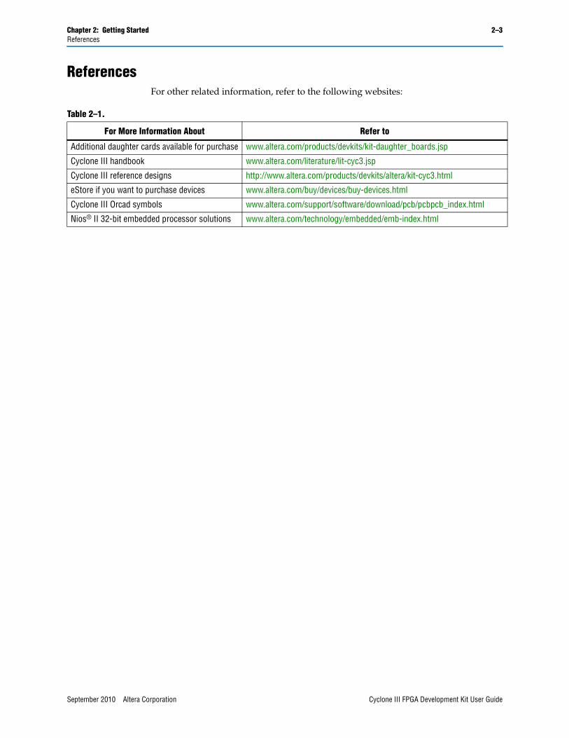
ReferencesFor other related information, refer to the following websites:
Table 2–1.
For More Information About Refer to
Additional daughter cards available for purchase www.altera.com/products/devkits/kit-daughter_boards.jsp
Cyclone III handbook www.altera.com/literature/lit-cyc3.jsp
Cyclone III reference designs http://www.altera.com/products/devkits/altera/kit-cyc3.html
eStore if you want to purchase devices www.altera.com/buy/devices/buy-devices.html
Cyclone III Orcad symbols www.altera.com/support/software/download/pcb/pcbpcb_index.html
Nios® II 32-bit embedded processor solutions www.altera.com/technology/embedded/emb-index.html
September 2010 Altera Corporation Cyclone III FPGA Development Kit User Guide

2–4 Chapter 2: Getting StartedReferences
Cyclone III FPGA Development Kit User Guide September 2010 Altera Corporation
September 2010 Altera Corporation
3. Software Installation
IntroductionThis section describes the following procedures:
■ “Installing the Cyclone III Development Kit”
■ “Installing the Quartus II Web Edition Software” on page 3–2
■ “Installing the USB-Blaster Driver” on page 3–3
1 Before starting the installation, verify that you have complied with the conditions described in “Software Requirements” on page 2–2.
Installing the Cyclone III Development KitThe license-free Cyclone III Development Kit installer includes all the documentation and design examples for the kit.
To install the Cyclone III Development Kit, follow these steps:
1. Download the Cyclone III Development Kit installer from the Cyclone III FPGA Development Kit page of the Altera website. Alternatively, you can request a development kit DVD from the Development Kits, Daughter Cards & Programming Hardware page of the Altera website.
2. Follow the on-screen instructions to complete the installation process.
When the installation is complete, the Cyclone III Development Kit installation program creates the directory structure shown in Figure 3–1, where <path> is the Cyclone III Development Kit installation directory.
Figure 3–1. Cyclone III Development Kit Installed Directory Structure
cycloneIII_3c120_dev
documents
examples
board_design_files
The default Windows installation directory is C:\altera\<version#>\kits.
factory_recovery
demos
<path>
Cyclone III FPGA Development Kit User Guide
3–2 Chapter 3: Software InstallationInstalling the Quartus II Web Edition Software
Table 3–1 lists the file directory names and a description of their contents.
Installing the Quartus II Web Edition SoftwareThe Quartus II Web Edition software provides the necessary tools for developing hardware and software for Altera FPGAs. Included in the Quartus II Web Edition software are the Quartus II software, the Nios II EDS, and the MegaCore® IP Library. The Quartus II software (including SOPC Builder) and the Nios II EDS are the primary FPGA development tools for creating the reference designs in this kit.
To install the Quartus II Web Edition software, follow these steps:
1. Download the Quartus II Web Edition software from the Quartus II Web Edition Software page of the Altera website. Alternatively, you can request a DVD from the Altera IP and Software DVD Request Form page of the Altera website.
2. Follow the on-screen instructions to complete the installation process.
f If you have difficulty installing the Quartus II software, refer to Quartus II Installation & Licensing for Windows and Linux Workstations.
The Quartus II Web Edition software includes the following items:
■ Quartus II software—The Quartus II software, including the SOPC Builder system development tool, provides a comprehensive environment for system-on-a-programmable-chip (SOPC) design. The Quartus II software integrates into nearly any design environment and provides interfaces to industry-standard EDA tools.
f To compare the Quartus II subscription and web editions, refer to Altera Quartus II Software—Subscription Edition vs. Web Edition. The kit also works with the subscription edition.
Table 3–1. Installed Directory Contents
Directory Name Description of Contents
board_design_files Contains schematic, layout, assembly, and bill of material board design files. Use these files as a starting point for a new prototype board design.
demos Contains demonstration applications that may change from release to release.
documents Contains the development kit documentation.
examples Contains the sample design files for the Cyclone III Development Kit.
factory_recovery Contains the original data programmed onto the board before shipment. Use this data to put the board into the original condition.
Cyclone III FPGA Development Kit User Guide September 2010 Altera Corporation
Chapter 3: Software Installation 3–3Installing the USB-Blaster Driver
■ MegaCore IP Library—A library that contains Altera IP MegaCore functions. You can evaluate MegaCore functions with the OpenCore Plus feature to perform the following tasks:
■ Simulate behavior of a MegaCore function in your system
■ Verify functionality of your design, and quickly and easily evaluate its size and speed
■ Generate time-limited device programming files for designs that include MegaCore functions
■ Program a device and verify your design in hardware
■ The OpenCore Plus hardware evaluation feature is an evaluation tool for prototyping only. You must purchase a license to use a MegaCore function in production.
f For more information about OpenCore Plus, refer to AN 320: OpenCore Plus Evaluation of Megafunctions.
■ Nios® II Embedded Design Suite (EDS)—A full-featured tool set that allow you to develop embedded software for the Nios II processor which you can include in your Altera FPGA designs.
Licensing ConsiderationsThe Quartus II Web Edition software is license-free and supports Cyclone III devices without any additional licensing requirement. This kit also works with the Quartus II Subscription Edition software, after you obtain the proper license file. To purchase a subscription, contact your Altera sales representative.
Installing the USB-Blaster DriverThe Cyclone III development board includes integrated USB-Blaster™ circuitry for FPGA programming. However, for the host computer and development board to communicate, you must install the USB-Blaster driver on the host computer.
f To download the USB-Blaster driver, go to the Altera support site at www.altera.com/support/software/drivers/dri-index.html.To install it, go to www.altera.com/support/software/drivers/usb-blaster/dri-usb-blaster-xp.html.
September 2010 Altera Corporation Cyclone III FPGA Development Kit User Guide

3–4 Chapter 3: Software InstallationInstalling the USB-Blaster Driver
Cyclone III FPGA Development Kit User Guide September 2010 Altera Corporation
September 2010 Altera Corporation
4. Development Board Setup
IntroductionThe instructions in this chapter explain how to install the development board and configure the FPGA.
RequirementsBefore starting the installation, verify that you have complied with the conditions described in “Hardware Requirements” on page 2–2 and have completed the following requirements:
■ Quartus II software installed on the host computer
■ USB-Blaster driver software installed on the host computer.
1 The Cyclone III development board includes integrated USB-Blaster circuitry for FPGA programming. Host computer and development board cannot communicate without the USB-Blaster driver software installed. For installation information, refer to “Installing the USB-Blaster Driver” on page 3–3.
Cyclone III FPGA Development Kit User Guide
4–2 Chapter 4: Development Board SetupPowering Up the Board
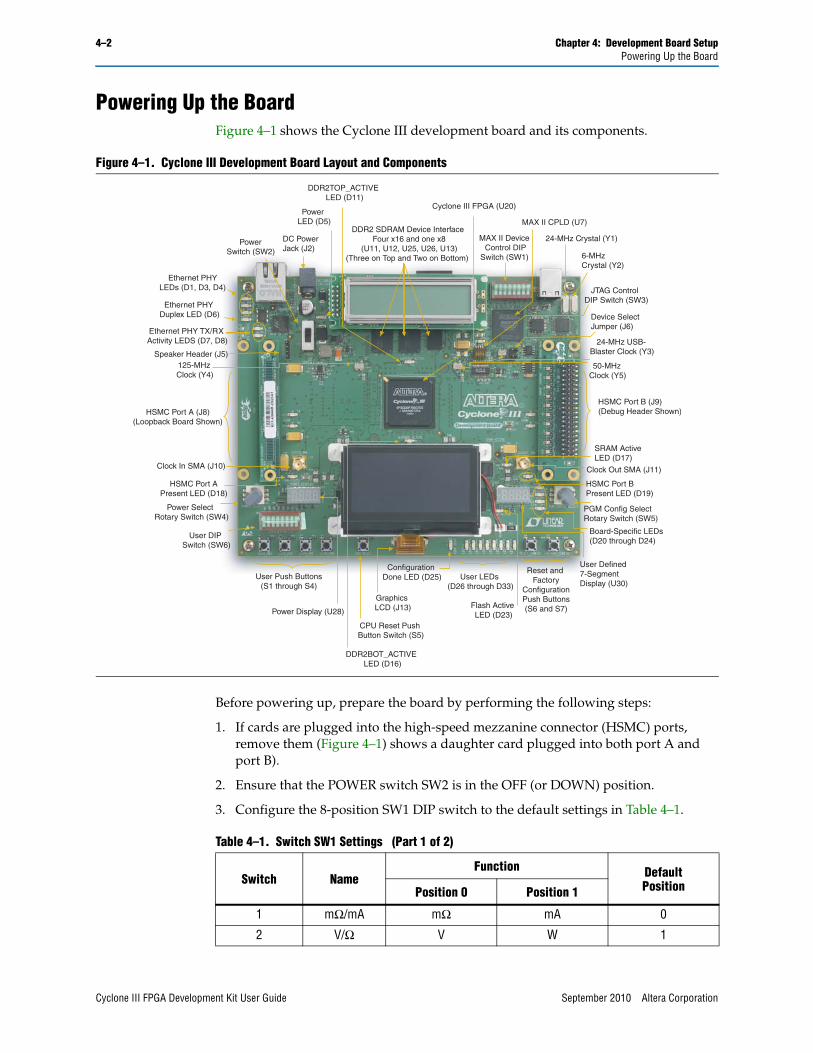
Powering Up the BoardFigure 4–1 shows the Cyclone III development board and its components.
Before powering up, prepare the board by performing the following steps:
1. If cards are plugged into the high-speed mezzanine connector (HSMC) ports, remove them (Figure 4–1) shows a daughter card plugged into both port A and port B).
2. Ensure that the POWER switch SW2 is in the OFF (or DOWN) position.
3. Configure the 8-position SW1 DIP switch to the default settings in Table 4–1.
Figure 4–1. Cyclone III Development Board Layout and Components
Speaker Header (J5)
DC PowerJack (J2)
Ethernet PHYLEDs (D1, D3, D4)
Ethernet PHY Duplex LED (D6)
PowerSwitch (SW2)
Power LED (D5)
Ethernet PHY TX/RX Activity LEDS (D7, D8)
MAX II CPLD (U7) DDR2 SDRAM Device Interface
Four x16 and one x8 (U11, U12, U25, U26, U13)
(Three on Top and Two on Bottom)
DDR2TOP_ACTIVE LED (D11)
Cyclone III FPGA (U20)
MAX II Device Control DIP
Switch (SW1)
24-MHz Crystal (Y1)
6-MHzCrystal (Y2)
Clock Out SMA (J11)
HSMC Port BPresent LED (D19)
PGM Config SelectRotary Switch (SW5)
User Push Buttons(S1 through S4)
User DIP Switch (SW6)
CPU Reset Push Button Switch (S5)
Power Select Rotary Switch (SW4)
User Defined7-SegmentDisplay (U30)
Board-Specific LEDs(D20 through D24)
SRAM ActiveLED (D17)
HSMC Port APresent LED (D18)
Clock In SMA (J10)
Power Display (U28)Flash Active LED (D23)
Configuration Done LED (D25) User LEDs
(D26 through D33)
Reset and Factory
Configuration Push Buttons (S6 and S7)
DDR2BOT_ACTIVE LED (D16)
50-MHz Clock (Y5)
125-MHz Clock (Y4)
24-MHz USB- Blaster Clock (Y3)
JTAG Control DIP Switch (SW3)
Graphics LCD (J13)
HSMC Port B (J9)(Debug Header Shown)HSMC Port A (J8)
(Loopback Board Shown)
Device SelectJumper (J6)
Table 4–1. Switch SW1 Settings (Part 1 of 2)
Switch NameFunction Default
PositionPosition 0 Position 1
1 mΩ/mA mΩ mA 0
2 V/Ω V W 1
Cyclone III FPGA Development Kit User Guide September 2010 Altera Corporation
Chapter 4: Development Board Setup 4–3Powering Up the Board
4. Ensure that the 4-position SW3 mini-DIP switches and the two jumpers are set to the default positions shown in Table 4–2.
5. Verify that the PGM CONFIG SELECT rotary switch SW5 is set to 0.
At power up, the development board uses a preloaded configuration to demonstrate that the board is operating correctly.
Power up the development board by performing the following steps:
1. Connect the 16-V DC adapter to the development board and to a power source.
w Use only the supplied 16-V power supply. Power regulation circuitry on the board could be damaged by supplies greater than 16 V.
2. Slide the POWER switch to ON. The nearby blue POWER light-emitting diode (LED) lights up.
3. Confirm that user LEDs 0-7 flash in a scrolling, side-to-side pattern. For customized configurations, the pattern depends on the application.
f For information about custom configurations, refer to “Programming the Flash Device” on page A–4.
3 RSV0 MAX_RESERVE0 X
4 RSV1 MAX_RESERVE1 X
5 MAX0 PFL Disable PFL Enable 1
6 MAX1 MAX_DIP1 X
7 MAX2 MAX_DIP2 X
8 MAX3 MAX_DIP3 X
Note to Table 4–1:
(1) X = don’t care
Table 4–2. Initial Switch and Jumper Settings
DEV_SEL-J6 JTAG_SEL-J7 SW3.1 SW3.2 SW3.3 SW3.4
ON ON ON OFF OFF OFF
Table 4–1. Switch SW1 Settings (Part 2 of 2)
Switch NameFunction Default
PositionPosition 0 Position 1
September 2010 Altera Corporation Cyclone III FPGA Development Kit User Guide
4–4 Chapter 4: Development Board SetupConfiguring the FPGA
Configuring the FPGABefore configuring the FPGA, ensure that the Quartus II software and the USB-Blaster driver software are installed on the host computer and the development board is powered on.
f For USB-Blaster driver installation information, refer to “Installing the USB-Blaster Driver” on page 3–3.
To configure the Cyclone III FPGA, perform the following steps:
1. Verify that the 4-position SW3 mini-DIP switches and the two jumpers are set to the default positions shown in Table 4–2.
2. Connect the USB cable to the development board USB port.
3. Cycle the POWER switch OFF then ON.
4. Start the Quartus II software.
5. On the Tools menu, click Programmer. The Quartus II Programmer appears.
6. Click Add File and select <path>\...\examples\cycloneIII_3c120_dev_my_first_fpga\cycloneIII_3c120_dev_my_first_fpga.sof.
7. Turn on Program/Configure to select the added file.
8. Click Start to download the selected file to the FPGA. The FPGA is configured when the progress bar reaches 100%.
9. Confirm that user LEDs 0-3 flash in a slow binary counting pattern.
Cyclone III FPGA Development Kit User Guide September 2010 Altera Corporation
September 2010 Altera Corporation
5. Board Update Portal
IntroductionThe Cyclone III FPGA Development Kit ships with the Board Update Portal design example stored in the factory portion of the flash memory on the board. The design consists of a Nios II embedded processor, an Ethernet MAC, and an HTML web server.
When you power up the board with the PGM CONFIG SELECT rotary switch (SW5) in position 0, the Cyclone III FPGA configures with the Board Update Portal design example. The design can obtain an IP address from any DHCP server and serve a web page from the flash on your board to any host computer on the same network. The web page allows you to upload new FPGA designs to the FPGA design 1 and design 6 (HW1 and SW1) portion of flash memory, and provides links to useful information on the Altera website, including links to kit-specific and design resources.
1 After successfully updating the FPGA design 1 and design 6 (HW1 and SW1)flash memory, you can load the user design from flash memory into the FPGA. To do so, set the PGM CONFIG SELECT rotary switch (SW5) to position 1 and power cycle the board.
The source code for the Board Update Portal design resides in the <install dir>\kits\cycloneIII_3c120_dev\examples directory. If the Board Update Portal is corrupted or deleted from the flash memory, refer to “Restoring the Factory Design to the Flash Device” on page A–6 to restore the board with its original factory contents.
Connecting to the Board Update Portal Web PageThis section provides instructions to connect to the Board Update Portal web page.
1 Before you proceed, ensure that you have the following:
■ A PC with a connection to a working Ethernet port on a DHCP enabled network.
■ A separate working Ethernet port connected to the same network for the board.
■ The Ethernet and power cables that are included in the kit.
To connect to the Board Update Portal web page, perform the following steps:
1. With the board powered down, set the PGM CONFIG SELECT rotary switch (SW5) to position 0.
2. Attach the Ethernet cable from the board to your LAN.
3. Power up the board. The board connects to the LAN’s gateway router, and obtains an IP address. The LCD on the board displays the IP address.
4. Launch a web browser on a PC that is connected to the same network, and enter the IP address from the LCD into the browser address bar. The Board Update Portal web page appears in the browser.
Cyclone III FPGA Development Kit User Guide
5–2 Chapter 5: Board Update PortalUsing the Board Update Portal to Update User Designs
5. Click Cyclone III FPGA Development Kit on the Board Update Portal web page to access the kit’s home page. Visit this page occasionally for documentation updates and additional new designs.
f You can also navigate directly to the Cyclone III FPGA Development Kit page of the Altera website to determine if you have the latest kit software.
Using the Board Update Portal to Update User DesignsThe Board Update Portal allows you to write new designs to the FPGA design 1 and design 6 (HW1 and SW1)portion of flash memory. Designs must be in the Nios II Flash Programmer File (.flash) format.
1 Design files available from the Cyclone III FPGA Development Kit page of the Altera website include .flash files. You can also create .flash files from your own custom design. Refer to “Creating a Flash File” on page A–1 for information about preparing your own design for upload.
To upload a design over the network into the FPGA design 1 and design 6 (HW1 and SW1) of flash memory on your board, perform the following steps:
1. Perform the steps in “Connecting to the Board Update Portal Web Page” to access the Board Update Portal web page.
2. In the Hardware File Name field specify the .flash file that you either downloaded from the Altera website or created on your own. If there is a software component to the design, specify it in the same manner using the Software File Name field, otherwise leave the Software File Name field blank.
3. Click Upload. The file takes about 20 seconds to upload.
4. To configure the FPGA with the new design after the flash memory upload process completes, set the PGM CONFIG SELECT rotary switch (SW5) to the 1 position and power cycle the board, or press the RESET_CONFIG push-button (S6).
1 As long as you do not overwrite the factory image in the flash memory device, you can continue to use the Board Update Portal to write new designs to the FPGA design 1 and design 6 (HW1 and SW1)portion of flash memory. If you overwrite the factory image, you can restore it by following the instructions in “Restoring the Factory Design to the Flash Device” on page A–6.
Cyclone III FPGA Development Kit User Guide September 2010 Altera Corporation
September 2010 Altera Corporation
6. Board Test System
IntroductionThe kit includes a design example and application called the Board Test System to test the functionality of the Cyclone III FPGA development board. The application provides an easy-to-use interface to alter functional settings and observe the results. You can use the application to test board components, modify functional parameters, observe performance, and measure power usage. The application is also useful as a reference for designing systems. To install the application, follow the steps in “Installing the Cyclone III Development Kit” on page 3–1.
The application provides access to the following Cyclone III FPGA development board features:
■ General purpose I/O (GPIO)
■ SRAM
■ Flash memory
■ DDR2 memory
■ Graphic LCD
The application allows you to exercise most of the board components. While using the application, you reconfigure the FPGA several times with test designs specific to the functionality you are testing.
Cyclone III FPGA Development Kit User Guide
6–2 Chapter 6: Board Test SystemPreparing the Board
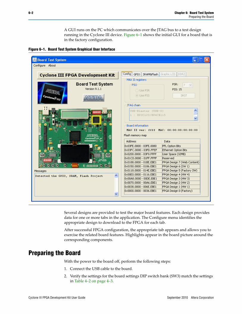
A GUI runs on the PC which communicates over the JTAG bus to a test design running in the Cyclone III device. Figure 6–1 shows the initial GUI for a board that is in the factory configuration.
Several designs are provided to test the major board features. Each design provides data for one or more tabs in the application. The Configure menu identifies the appropriate design to download to the FPGA for each tab.
After successful FPGA configuration, the appropriate tab appears and allows you to exercise the related board features. Highlights appear in the board picture around the corresponding components.
Preparing the BoardWith the power to the board off, perform the following steps:
1. Connect the USB cable to the board.
2. Verify the settings for the board settings DIP switch bank (SW3) match the settings in Table 4–2 on page 4–3.
Figure 6–1. Board Test System Graphical User Interface
Cyclone III FPGA Development Kit User Guide September 2010 Altera Corporation
Chapter 6: Board Test System 6–3Running the Board Test System
3. Set the PGM CONFIG SELECT rotary switch (SW5) to position 1.
4. Turn the power to the board on. The board loads the design stored in the user hardware 1 portion of flash memory into the FPGA. If your board is still in the factory configuration or if you have downloaded a newer version of the Board Test System to flash memory through the Board Update Portal, the design that loads tests accessing the GPIO, SRAM, and flash memory.
c To ensure operating stability, keep the USB cable connected and the board powered on when running the demonstration application. The application cannot run correctly unless the USB cable is attached and the board is on.
Running the Board Test SystemTo run the application, navigate to the <install dir>\kits\cycloneIII_3c120_dev\examples\board_test_system directory and run the BoardTestSystem.exe application.
1 On Windows, click Start > All Programs > Altera > Cyclone III FPGA Development Kit <version> > Board Test System to run the application.
A GUI appears, displaying the application tab that corresponds to the design running in the FPGA. The Cyclone III FPGA development board’s flash memory ships preconfigured with the design that corresponds to the Config, GPIO, SRAM&Flash tabs.
1 If you power up your board with the PGM CONFIG SELECT rotary switch (SW5) in a position other than position 1, or if you load your own design into the FPGA with the Quartus II Programmer, you receive a message prompting you to configure your board with a valid Board Test System design. Refer to “The Configure Menu” for information about configuring your board.
September 2010 Altera Corporation Cyclone III FPGA Development Kit User Guide
6–4 Chapter 6: Board Test SystemUsing the Board Test System
Using the Board Test SystemThis section describes each control in the Board Test System application.
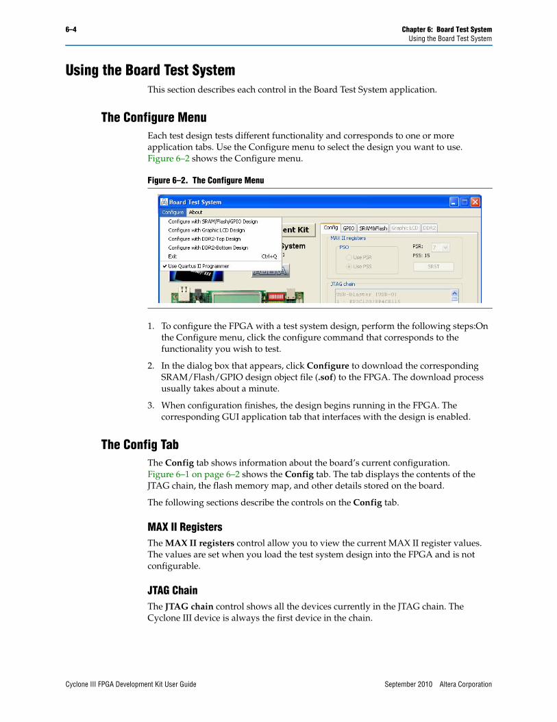
The Configure MenuEach test design tests different functionality and corresponds to one or more application tabs. Use the Configure menu to select the design you want to use. Figure 6–2 shows the Configure menu.
1. To configure the FPGA with a test system design, perform the following steps:On the Configure menu, click the configure command that corresponds to the functionality you wish to test.
2. In the dialog box that appears, click Configure to download the corresponding SRAM/Flash/GPIO design object file (.sof) to the FPGA. The download process usually takes about a minute.
3. When configuration finishes, the design begins running in the FPGA. The corresponding GUI application tab that interfaces with the design is enabled.
The Config TabThe Config tab shows information about the board’s current configuration. Figure 6–1 on page 6–2 shows the Config tab. The tab displays the contents of the JTAG chain, the flash memory map, and other details stored on the board.
The following sections describe the controls on the Config tab.
MAX II RegistersThe MAX II registers control allow you to view the current MAX II register values. The values are set when you load the test system design into the FPGA and is not configurable.
JTAG ChainThe JTAG chain control shows all the devices currently in the JTAG chain. The Cyclone III device is always the first device in the chain.
Figure 6–2. The Configure Menu
Cyclone III FPGA Development Kit User Guide September 2010 Altera Corporation
Chapter 6: Board Test System 6–5Using the Board Test System
1 Connecting a jumper shunt on J6 and an external USB-Blaster on J14 includes the MAX II device in the JTAG chain.
Board InformationThe Board information controls display static information about your board.
Flash Memory MapThe Flash memory map control shows the memory map of the flash memory device on your board.
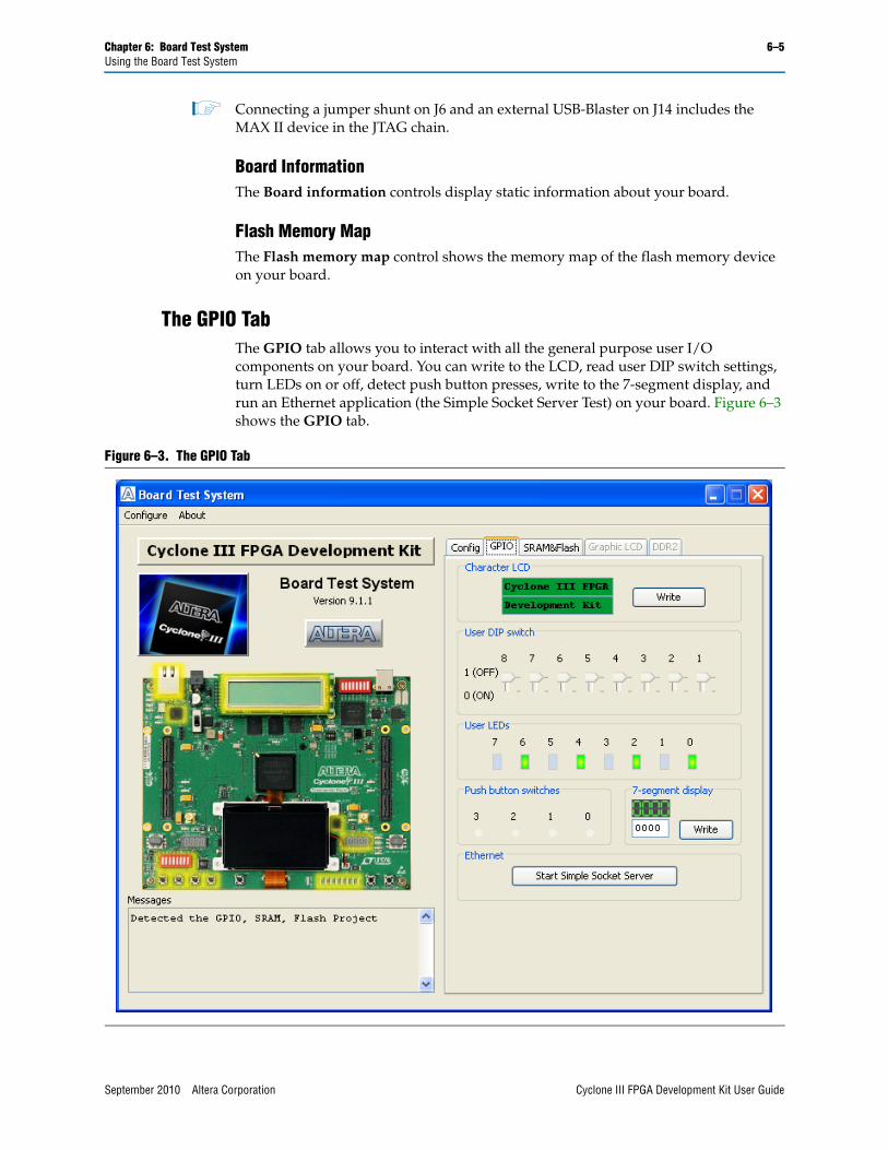
The GPIO TabThe GPIO tab allows you to interact with all the general purpose user I/O components on your board. You can write to the LCD, read user DIP switch settings, turn LEDs on or off, detect push button presses, write to the 7-segment display, and run an Ethernet application (the Simple Socket Server Test) on your board. Figure 6–3 shows the GPIO tab.
Figure 6–3. The GPIO Tab
September 2010 Altera Corporation Cyclone III FPGA Development Kit User Guide
6–6 Chapter 6: Board Test SystemUsing the Board Test System
The following sections describe the controls on the GPIO tab.
Character LCDThe Character LCD controls allow you to display text strings on the character LCD on your board. Type text in the text boxes and then click Write.
1 If you exceed the 16 character display limit on either line, a warning message appears.
User DIP SwitchesThe read-only User DIP switches control displays the current positions of the switches in the user DIP switch bank (SW6). Change the switches on the board to see the graphical display change accordingly.
User LEDsThe User LEDs control displays the current state of the user LEDs. Click the graphical representation of the LEDs to turn the board LEDs on and off.
Push Button SwitchesThe read-only Push button switches control displays the current state of the board user push buttons. Press a push button (S1-S4) on the board to see the graphical display change accordingly.
7-Segment DisplayThe 7-segment display control allow you to display hexadecimal numbers on the 7-segment display on your board. Type number in the text box and then click Write.
1 If you enter a hexadecimal value outside of the 0x0000 to 0xFFFF display limit, a warning message identifies the valid hexadecimal value range.
EthernetThe Ethernet control allows you to run an Ethernet application (the Simple Socket Server Test) on your board.
Click Start Simple Socket Server to load the application which allows you to interactively enter keyboard characters to select menu items. The application responds to the keypress and takes appropriate action.
Cyclone III FPGA Development Kit User Guide September 2010 Altera Corporation
Chapter 6: Board Test System 6–7Using the Board Test System
The SRAM&Flash TabThe SRAM&Flash tab allows you to read and write SRAM and flash memory on your board. Figure 6–4 shows the SRAM&Flash tab.
The following sections describe the controls on the SRAM&Flash tab.
SRAMThe SRAM control allows you to read and write the SRAM on your board. Type a starting address in the text box and click Read. Values starting at the specified address appear in the top row of the table. The SRAM addresses display in the format the Nios II processor within the FPGA uses, that is, each SRAM address is offset by 0x00000000. Thus, the first location in SRAM appears as 0x00000000 in the GUI. The base address of SRAM in this Nios II-based BTS design is 0x0D00.0000. The valid address range within the 2-MB SRAM is 0x0000.0000 through 0x001F.FFFF, as shown in the GUI.
1 If you enter an address outside of the 0x00000000 to 0x001FFF80 SRAM address space, a warning message identifies the valid SRAM address range.
Figure 6–4. The SRAM&Flash Tab
September 2010 Altera Corporation Cyclone III FPGA Development Kit User Guide
6–8 Chapter 6: Board Test SystemUsing the Board Test System
To update the SRAM contents, change values in the table and click Write. The application writes the new values to SRAM and then reads the values back to guarantee that the graphical display accurately reflects the memory contents.
FlashThe Flash control allows you to read and write the flash memory on your board. Type a starting address in the text box and click Read. Values starting at the specified address appear in the top row of the table. The flash memory addresses display in the format the Nios II processor within the FPGA uses, that is, each flash memory address is offset by 0x00000000. Thus, the first location in flash memory appears as 0x00000000 in the GUI. The base address of flash memory in this Nios II-based BTS design is 0x0800.0000. The valid address range within the 64-MB flash memory is 0x0000.0000 through 0x03FF.FFFF, as shown in the GUI.
1 If you enter an address outside of the 0x00000000 to 0x03FFFF80 flash memory address space, a warning message identifies the valid flash memory address range.
To update the flash memory contents, change values in the table and click Write. The application writes the new values to flash memory and then reads the values back to guarantee that the graphical display accurately reflects the memory contents.
1 To prevent overwriting the dedicated portions of flash memory, the application limits the writable flash memory address range from 0x07000000 to 0x0701FF80 (which corresponds to the unused flash memory address range of 0x02000000 - 0x0201FF80 shown in Figure 6–1 on page 6–2).
Cyclone III FPGA Development Kit User Guide September 2010 Altera Corporation
Chapter 6: Board Test System 6–9Using the Board Test System
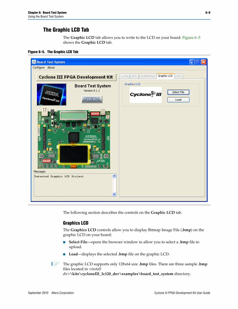
The Graphic LCD TabThe Graphic LCD tab allows you to write to the LCD on your board. Figure 6–3 shows the Graphic LCD tab.
The following section describes the controls on the Graphic LCD tab.
Graphics LCDThe Graphics LCD controls allow you to display Bitmap Image File (.bmp) on the graphic LCD on your board:
■ Select File—opens the browser window to allow you to select a .bmp file to upload.
■ Load—displays the selected .bmp file on the graphic LCD.
1 The graphic LCD supports only 128x64 size .bmp files. There are three sample .bmp files located in <install dir>\kits\cycloneIII_3c120_dev\examples\board_test_system directory.
Figure 6–5. The Graphic LCD Tab
September 2010 Altera Corporation Cyclone III FPGA Development Kit User Guide
6–10 Chapter 6: Board Test SystemUsing the Board Test System
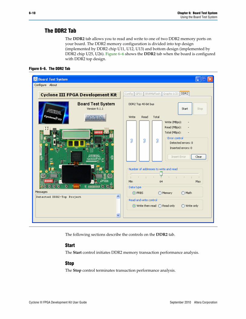
The DDR2 TabThe DDR2 tab allows you to read and write to one of two DDR2 memory ports on your board. The DDR2 memory configuration is divided into top design (implemented by DDR2 chip U11, U12, U13) and bottom design (implemented by DDR2 chip U25, U26). Figure 6–6 shows the DDR2 tab when the board is configured with DDR2 top design.
The following sections describe the controls on the DDR2 tab.
StartThe Start control initiates DDR2 memory transaction performance analysis.
StopThe Stop control terminates transaction performance analysis.
Figure 6–6. The DDR2 Tab
Cyclone III FPGA Development Kit User Guide September 2010 Altera Corporation
Chapter 6: Board Test System 6–11Using the Board Test System
Performance IndicatorsThese controls display current transaction performance analysis information collected since you last clicked Start:
■ Write, Read, and Total performance bars—show the percentage of maximum theoretical data rate that the requested transactions are able to achieve.
■ Write(MBps), Read(MBps), and Total(MBps)—show the number of bytes of data analyzed per second. For DDR2 top design, the data bus is 40-bits wide and the frequency is 300 MHz double data rate, equating to a theoretical maximum bandwidth of 1500 MBps. For DDR2 bottom design, the data bus is 32-bits wide and the frequency is 300 MHz double data rate, equating to a theoretical maximum bandwidth of 1200 MBps.
Error ControlThe Error control controls display data errors detected during analysis and allow you to insert errors:
■ Detected errors—displays the number of data errors detected in the hardware.
■ Inserted errors—displays the number of errors inserted into the transaction stream.
■ Insert Error—inserts a one-word error into the transaction stream each time you click the button. Insert Error is only enabled during transaction performance analysis.
■ Clear—resets the Detected errors and Inserted errors counters to zeros.
Number of Addresses to Write and ReadThe Number of addresses to write and read control determines the number of addresses to use in each iteration of reads and writes. Valid values range from 8 to 8,192.
Data TypeThe Data type control specifies the type of data contained in the transactions. The following data types are available for analysis:
■ PRBS—selects pseudo-random bit sequences.
■ Memory—selects a generic data pattern stored in the on-chip memory of the Cyclone III device.
■ Math—selects data generated from a simple math function within the FPGA fabric.
Read and Write ControlThe Read and write control specifies the type of transactions to analyze. The following transaction types are available for analysis:
■ Write then read—selects read and write transactions for analysis.
■ Read only—selects read transactions for analysis.
■ Write only—selects write transactions for analysis.
September 2010 Altera Corporation Cyclone III FPGA Development Kit User Guide

6–12 Chapter 6: Board Test SystemUsing the Board Test System
Cyclone III FPGA Development Kit User Guide September 2010 Altera Corporation
September 2010 Altera Corporation
7. Power Measurement
IntroductionOne of the main features of the Cyclone III FPGA device is its low power consumption. You can measure the power used by the 3C120 FPGA device on the Cyclone III development board for various conditions with a power design example provided with the kit.
With the power design example you can control the amount of logic utilized in the FPGA, the clock frequency, and the number of I/Os used, and measure the effect on power used by the Cyclone III device.
Power Design ExampleThe power design example uses a replicated module, stamp.v, that contains combinational logic, randomly filled ROMs, multiplier blocks, and shift registers that change with every clock cycle. The frequency and resource states indicated in Table 7–2 and Table 7–3 on page 7–2, respectively, represent the percent of the full design used. As compiled, the full example design uses the following FPGA resources:
■ Total logic elements: 111,673 / 119,088 (94%)
■ Total combinational functions: 12,293 / 119,088 (10%)
■ Dedicated logic registers: 104,192 / 119,088 (87%)
■ Total registers: 104,192
■ Total pins: 165 / 532 (31%)
■ Total virtual pins: 0
■ Total memory bits: 2,490,368 / 3,981,312 (63%)
■ Embedded multiplier 9-bit elements: 576 / 576 (100%)
■ Total phase-locked loops (PLLs): 1/4 (25%)
Table 7–1 describes the functionality of the four user push buttons that control the power design example. The on-board 50-MHz oscillator provides the input clock (i_clk, PIN_AH15).
Table 7–1. Four Input Button Functionality
User Push Button FPGA Pin Type Description
User_PB0 AD7 Reset Resets the demo to the beginning, i_nrst
User_PB1 AC12 Toggle Advances the design example to the next higher frequency, i_nfreq_next
User_PB2 AH3 Toggle Advances the design example to the next higher resource utilization, i_nperc_next
User_PB3 AA12 Toggle Enables the outputs to toggle, i_noutput_ena
Cyclone III FPGA Development Kit User Guide
7–2 Chapter 7: Power MeasurementPower Design Example
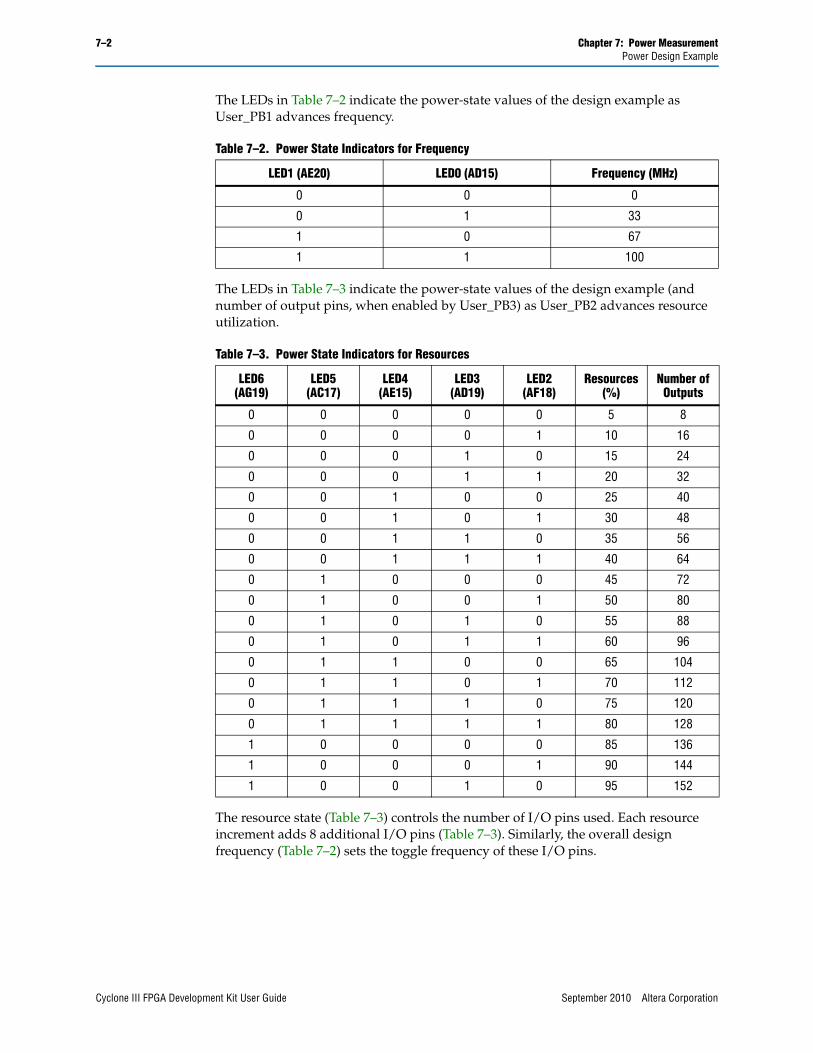
The LEDs in Table 7–2 indicate the power-state values of the design example as User_PB1 advances frequency.
The LEDs in Table 7–3 indicate the power-state values of the design example (and number of output pins, when enabled by User_PB3) as User_PB2 advances resource utilization.
The resource state (Table 7–3) controls the number of I/O pins used. Each resource increment adds 8 additional I/O pins (Table 7–3). Similarly, the overall design frequency (Table 7–2) sets the toggle frequency of these I/O pins.
Table 7–2. Power State Indicators for Frequency
LED1 (AE20) LED0 (AD15) Frequency (MHz)
0 0 0
0 1 33
1 0 67
1 1 100
Table 7–3. Power State Indicators for Resources
LED6(AG19)
LED5(AC17)
LED4(AE15)
LED3(AD19)
LED2(AF18)
Resources(%)
Number of Outputs
0 0 0 0 0 5 8
0 0 0 0 1 10 16
0 0 0 1 0 15 24
0 0 0 1 1 20 32
0 0 1 0 0 25 40
0 0 1 0 1 30 48
0 0 1 1 0 35 56
0 0 1 1 1 40 64
0 1 0 0 0 45 72
0 1 0 0 1 50 80
0 1 0 1 0 55 88
0 1 0 1 1 60 96
0 1 1 0 0 65 104
0 1 1 0 1 70 112
0 1 1 1 0 75 120
0 1 1 1 1 80 128
1 0 0 0 0 85 136
1 0 0 0 1 90 144
1 0 0 1 0 95 152
Cyclone III FPGA Development Kit User Guide September 2010 Altera Corporation
Chapter 7: Power Measurement 7–3Measuring Power
Measuring PowerYou can measure power by using the analog-to-digital (A/D) circuitry on the development board or by using a digital multi-meter (DMM) across on-board sense resistors. However, note that, depending on the DMM accuracy, the on-board A/D measurements tend to produce considerably more accurate results.
A/D MeasurementsThe POWER SELECT rotary switch SW4 sets the development board to measure and display FPGA core power or I/O output power (Table 7–4).
Measuring VCC_INT PowerTo measure FPGA core power at VCC_INT = 1.2 V for various power states, perform the following steps:
1. Ensure that the 8-position SW1 DIP switch is configured to the default settings shown in Table 4–1 on page 4–2.
2. Download the cycloneIII_3c120_dev_power_demo.sof file as described in “Configuring the FPGA” on page 4–4. You can find the power design example in<path>\...\examples\cycloneIII_3c120_dev_power_demo.
3. Set the POWER SELECT rotary switch SW4 to 0 to measure the internal VCC_INT power in watts.
4. Observe the power on the 4-digit hexadecimal power display. The on-board power measurements are performed at a high rate. For this reason, it appears that the display is dithering; however, what is actually taking place is the very fast momentary changes on the power rail.
5. Using the user input push buttons (Table 7–1 on page 7–1), advance through the power states in Table 7–2 and Table 7–3 on page 7–2. Notice how power increases as frequency and resources increase.
f For information about measuring power sources, refer to the Cyclone III 3C120 Development Board Reference Manual.
Measuring I/O PowerThis example uses FPGA I/O banks 1, 2, 5, and 6. Using the SW4 settings (Table 7–4), measure the power for I/O banks 1 and 2, then for I/O banks 5 and 6, by performing the following steps:
1. Ensure that the 8-position SW1 DIP switch is configured to the default settings shown in Table 4–1 on page 4–2.
Table 7–4. Switch SW4 Power Selection
Switch Position FPGA Power I/O Banks
0 Core: VCC_INT, 1.2 V —
5 I/O: 2.5 V 1 and 2
6 I/O: 2.5 V 5 and 6
September 2010 Altera Corporation Cyclone III FPGA Development Kit User Guide
7–4 Chapter 7: Power MeasurementMeasuring Power
2. Download the cycloneIII_dev_powerdemo.sof file as described in “Configuring the FPGA” on page 4–4. The power design example is in<path>\...\examples\cycloneIII_3c120_dev_powerdemo.
3. Set the POWER SELECT rotary switch SW4 to 5.
4. Observe the 4-digit hexadecimal display for the I/O output power in watts on banks 1 and 2.
5. Using the user input push buttons (Table 7–1 on page 7–1), advance through the power states in Table 7–2 and Table 7–3 on page 7–2. Notice how power increases as frequency and resources increase.
6. Press the User_PB3 button to enable the output pins on the HSMC connectors J8 and J9. LED7 (AF19), signal o_noutput_ena_state, lights to indicate that the outputs are enabled and toggling. Enabling the outputs further increases power for each resource utilization percentage used by the Cyclone III FPGA.
7. Press the User_PB3 button again to disable the outputs. LED7 turns off.
8. Set the POWER SELECT rotary switch SW4 to 6.
9. Repeat steps 4 through 7 to observe the I/O output power in watts on banks 5 and 6.
The sum of power results from the two sets of I/O banks provides the total FPGA I/O power.
f For specific information about on-board measurements and the POWER SELECT rotary switch, refer to the Cyclone III 3C120 Development Board Reference Manual.
Measuring Voltage with a DMMTo obtain power values by using a DMM, measure voltage across the sense resistors, R49, R48, and R51 on the board, then use the voltage measurements to calculate power.
1 For best results, use a DMM with six-digit for greater accuracy.
FPGA I/O power is distributed by banks (Table 7–5), for which the sense resistors are components R48 and R51. For the I/O power calculation, use the sum of voltage measurements across these resistors while outputs are enabled. For the FPGA core power calculation, measure the sense resistor voltage across R49.
Table 7–5. Sense Resistors
FPGA Power Voltage SenseResistor
ResistorValue
I/OBanks 1 and 2 2.5 V R48 0.009 Ω
Banks 5 and 6 2.5 V R51 0.009 Ω
Core: VCC_INT 1.2 V R49 0.009 Ω
Cyclone III FPGA Development Kit User Guide September 2010 Altera Corporation
Chapter 7: Power Measurement 7–5Changing the Design Example
Calculating PowerTo obtain the power P in watts, measure the voltage across the sense resistors, VSENSE, and calculate the nominal power as follows:
If
VSENSE = Voltage measured across the sense resistorISENSE = Current through the sense resistorVSUPPLY = FPGA supply voltageRSENSE = Sense resistor value in Table 7–5.
then
where
VSUPPLY is 1.2 V for the FPGA core and 2.5 V for FPGA I/O.
Voltage measurements on the DMM should increase as frequency and resource utilization increases according to Table 7–2 and Table 7–3 on page 7–2.
Changing the Design ExampleThe development kit includes source code for the Cyclone III power design example so you can use it as a starting point for your own measurements.
The design example uses 19 stamp.v modules, each with 8 outputs, for a total of 152 output pins. It assigns the pins selected as outputs to the HSMC connectors J8 and J9.
To change the number of outputs, modify the design example and assign the pins appropriately.
1 Power should track linearly with frequency and percentage resources. If you observe superlinear power measurements, some temperature issue may be the cause.
Equation 7–1.
VI VSUPPLY ISENSE×VSUPPLY VSENS×
RSENSE-----------------------------------------------== =
September 2010 Altera Corporation Cyclone III FPGA Development Kit User Guide

7–6 Chapter 7: Power MeasurementChanging the Design Example
Cyclone III FPGA Development Kit User Guide September 2010 Altera Corporation
September 2010 Altera Corporation
8. Design Tutorials
IntroductionThe example designs and tutorials included in the Cyclone III Development Kit help familiarize new users with development board features. My First FPGA Design Tutorial and My First Nios II Software Tutorial provide step-by-step guidance for the first-time user.
My First FPGA TutorialMy First FPGA Design Tutorial describes how to create a simple Altera FPGA design. The tutorial takes less than an hour to complete and provides an overview of the design flow using the Quartus II software to build a simple logic counter which drives LEDs to flash on the development board.
After installing the Cyclone III Development Kit, the My First FPGA Design Tutorial design and documentation can be found at <path>\...\documents\tutorials\hardware_tutorials\my_first_fpga_tutorial.pdf.
My First Nios II Software TutorialMy First Nios II Software Tutorial introduces the basic system development flow for the Nios II processor. This tutorial provides a good starting point if you are new to the Nios II processor or to the general concept of using an embedded processor in an FPGA. In this tutorial, you use a standard, existing Nios II hardware system and create a software program to run on it.
After installing the Cyclone III Development Kit, the My First Nios II Software Tutorial design and documentation can be found at <path>\...\documents\tutorials\software_tutorials\my_first_nios2_software_tutorial.pdf.
Cyclone III FPGA Development Kit User Guide

8–2 Chapter 8: Design TutorialsMy First Nios II Software Tutorial
Cyclone III FPGA Development Kit User Guide September 2010 Altera Corporation
September 2010 Altera Corporation
A. Programming the Flash Device
OverviewThere is a Common Flash Interface (CFI) type flash memory device on the Cyclone III development board. When you first receive the kit, this CFI flash device arrives programmed with a default factory configuration that was loaded from a Programmer Object File (.pof).
When you power up the board, the CFI flash device configures the FPGA with the default factory configuration using Passive Serial (PS) programming. If the configuration loads correctly, the user LEDs on the board flash sequentially from side to side.
As you develop your own project using the Altera tools, you may wish to program the flash device so that, upon power up, it loads the FPGA with your own design. Or you may wish to restore the default factory configuration to your board.
This appendix describes how to program the flash device. You can load an existing design from a .pof, but if your design exists only as an SRAM Object File (.sof), then first you must convert the .sof to a .pof. Programming the flash device also requires the use of the Altera parallel flash loader (PFL). Using this appendix, you can do the following:
■ Create a flash file by converting a .sof to .pof
■ Install the PFL
■ Use the Quartus II Programmer to write a .pof to the flash device
■ Restore the default factory configuration
Creating a Flash FileTo create a flash-programmable configuration .pof, perform the following steps:
1. On the File menu in the Quartus II software, click Convert Programming Files.
2. In the Convert Programming Files dialog box, select the parameter values as shown in the following table:
Table A–1.
Parameter Value
Programming file type Programmer Object File (.pof)
Configuration device CFI_512MB
Mode 1-bit Passive Serial
File name
<output_file.pof>
This is the default file name. Change this to the file name you wish to use for your application. Save the file in< path>\...\examples\cycloneIII_3c120_dev_pfl.
Memory Map File selected (default)
Cyclone III FPGA Development Kit User Guide
A–2 Appendix A: Programming the Flash DeviceCreating a Flash File
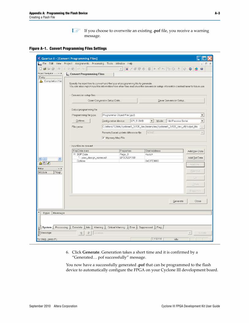
3. Click Options. In the Options dialog box, enter 0x3FE0000 and click OK. This sets the option bit base address for the development kit to the required default, 0x3FE0000. The option bit sector stores the start address for each page of memory and also stores the Page Valid bits. The Page Valid bits indicate whether each page is successfully programmed.
f For more information about option bits and Page Mode Implementation of memory, refer to Parallel Flash Loader Megafunction User Guide.
4. Choose the .sof file you want to convert by selecting the row labeled SOF Data in the Input files to convert area and click Add File.
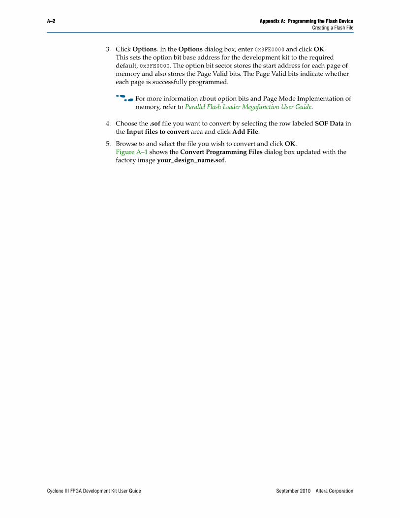
5. Browse to and select the file you wish to convert and click OK.Figure A–1 shows the Convert Programming Files dialog box updated with the factory image your_design_name.sof.
Cyclone III FPGA Development Kit User Guide September 2010 Altera Corporation
Appendix A: Programming the Flash Device A–3Creating a Flash File
1 If you choose to overwrite an existing .pof file, you receive a warning message.
6. Click Generate. Generation takes a short time and it is confirmed by a “Generated… pof successfully” message.
You now have a successfully generated .pof that can be programmed to the flash device to automatically configure the FPGA on your Cyclone III development board.
Figure A–1. Convert Programming Files Settings
September 2010 Altera Corporation Cyclone III FPGA Development Kit User Guide
A–4 Appendix A: Programming the Flash DeviceParallel Flash Loader Instantiation
Parallel Flash Loader InstantiationThe development kit includes a PFL megafunction design, cycloneIII_3c120_dev_pfl, in the directory <path>\...\examples. The Quartus II software uses the PFL to write programming files to the flash device, which then loads the FPGA on power up.
To write to a flash device, you must first program the PFL into the FPGA by using the Quartus II software as described in “Programming the Flash Device”, steps 1 through 8.
f For more information about the PFL megafunction, refer to Parallel Flash Loader Megafunction User Guide.
Programming the Flash DeviceTo program the flash device on the development board, you must first create a .pof flash file as described in “Creating a Flash File” on page A–1. The following procedure describes programming the PFL into the FPGA first, then uses the PFL to write the .pof flash file into the flash device.
To download a configuration bit stream into the flash device, perform the following steps:
1. Ensure that the POWER switch SW2 is in the OFF (or DOWN) position.
2. Verify the switch SW3 and jumper settings shown in Table 4–2 on page 4–3.
3. Connect the USB cable to the USB port on the board.
4. Cycle the POWER switch OFF then ON.
5. On the Tools menu in the Quartus II software, click Programmer.
6. Click Add File and select <path>\...\examples\cycloneIII_3C120_dev_pfl\cycloneIII_3C120_dev_pfl.sof.
7. Turn on the Program/Configure option for the added file.
Cyclone III FPGA Development Kit User Guide September 2010 Altera Corporation
Appendix A: Programming the Flash Device A–5Programming the Flash Device
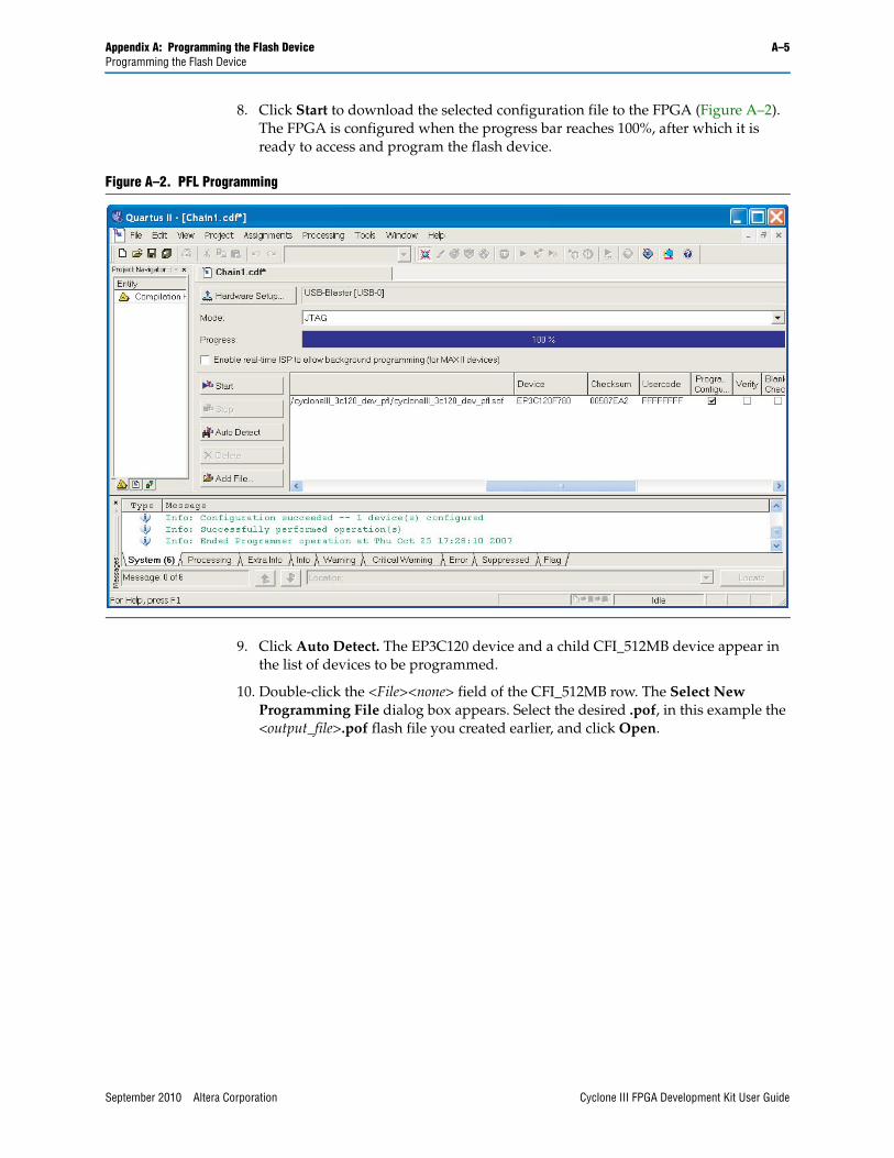
8. Click Start to download the selected configuration file to the FPGA (Figure A–2). The FPGA is configured when the progress bar reaches 100%, after which it is ready to access and program the flash device.
9. Click Auto Detect. The EP3C120 device and a child CFI_512MB device appear in the list of devices to be programmed.
10. Double-click the <File><none> field of the CFI_512MB row. The Select New Programming File dialog box appears. Select the desired .pof, in this example the <output_file>.pof flash file you created earlier, and click Open.
Figure A–2. PFL Programming
September 2010 Altera Corporation Cyclone III FPGA Development Kit User Guide
A–6 Appendix A: Programming the Flash DeviceRestoring the Factory Design to the Flash Device
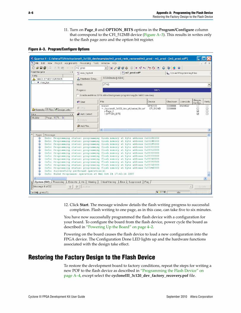
11. Turn on Page_0 and OPTION_BITS options in the Program/Configure column that correspond to the CFI_512MB device (Figure A–3). This results in writes only to the flash page zero and the option bit register.
12. Click Start. The message window details the flash writing progress to successful completion. Flash writing to one page, as in this case, can take five to six minutes.
You have now successfully programmed the flash device with a configuration for your board. To configure the board from the flash device, power cycle the board as described in “Powering Up the Board” on page 4–2.
Powering on the board causes the flash device to load a new configuration into the FPGA device. The Configuration Done LED lights up and the hardware functions associated with the design take effect.
Restoring the Factory Design to the Flash DeviceTo restore the development board to factory conditions, repeat the steps for writing a new POF to the flash device as described in “Programming the Flash Device” on page A–4, except select the cycloneIII_3c120_dev_factory_recovery.pof file.
Figure A–3. Program/Configure Options
Cyclone III FPGA Development Kit User Guide September 2010 Altera Corporation
September 2010 Altera Corporation
Additional Information
This chapter provides additional information about the document and Altera.
Document Revision HistoryThe following table shows the revision history for this document.
How to Contact AlteraTo locate the most up-to-date information about Altera products, refer to the following table.
Date Version Changes
September 2010 1.4■ Added Chapter 5, Board Update Portal and Chapter 6, Board Test System.
■ Converted document to new frame template and made textual and style changes.
July 2010 1.3
■ Updated Figure 3–1 on page 3–1.
■ Updated “Installing the Quartus II Web Edition Software” on page 3–2.
■ Updated Table 2–1 on page 2–3.
■ Updated Copyright information.
■ General formatting edits.
March 2009 1.2 Updated Table 4–2 on page 4–3.
August 2008 1.1
■ Updated “Introduction” section.
■ Updated directory structure and information about the directory contents in Figure 3–1 and Table 3–1, respectively.
■ Removed Figure 3-2 and Figure 4-2.
■ Corrected SW3.4 information in Table 4–2.
■ Updated “Power Design Example” section with new compilation numbers.
■ Updated “Measuring Power” section.
■ Converted document to new frame template and made textual and style changes.
October 2007 1.0 First publication
Contact (1) Contact Method Address
Technical support Website www.altera.com/support
Technical trainingWebsite www.altera.com/training
Email [email protected]
Product literature Website www.altera.com/literature
Non-technical support (General) Email [email protected]
(Software Licensing) Email [email protected]
Note to Table:
(1) You can also contact your local Altera sales office or sales representative.
Cyclone III FPGA Development Kit User Guide
Info–2 Additional InformationTypographic Conventions
Typographic ConventionsThe following table shows the typographic conventions this document uses.
Visual Cue Meaning
Bold Type with Initial Capital Letters
Indicate command names, dialog box titles, dialog box options, and other GUI labels. For example, Save As dialog box. For GUI elements, capitalization matches the GUI.
bold typeIndicates directory names, project names, disk drive names, file names, file name extensions, software utility names, and GUI labels. For example, \qdesigns directory, D: drive, and chiptrip.gdf file.
Italic Type with Initial Capital Letters Indicate document titles. For example, Stratix IV Design Guidelines.
italic typeIndicates variables. For example, n + 1.
Variable names are enclosed in angle brackets (< >). For example, <file name> and <project name>.pof file.
Initial Capital Letters Indicate keyboard keys and menu names. For example, the Delete key and the Options menu.
“Subheading Title” Quotation marks indicate references to sections within a document and titles of Quartus II Help topics. For example, “Typographic Conventions.”
Courier type
Indicates signal, port, register, bit, block, and primitive names. For example, data1, tdi, and input. The suffix n denotes an active-low signal. For example, resetn.
Indicates command line commands and anything that must be typed exactly as it appears. For example, c:\qdesigns\tutorial\chiptrip.gdf.
Also indicates sections of an actual file, such as a Report File, references to parts of files (for example, the AHDL keyword SUBDESIGN), and logic function names (for example, TRI).
r An angled arrow instructs you to press the Enter key.
1., 2., 3., anda., b., c., and so on
Numbered steps indicate a list of items when the sequence of the items is important, such as the steps listed in a procedure.
■ ■ ■ Bullets indicate a list of items when the sequence of the items is not important.
1 The hand points to information that requires special attention.
A question mark directs you to a software help system with related information.
f The feet direct you to another document or website with related information.
c A caution calls attention to a condition or possible situation that can damage or destroy the product or your work.
w A warning calls attention to a condition or possible situation that can cause you injury.
The envelope links to the Email Subscription Management Center page of the Altera website, where you can sign up to receive update notifications for Altera documents.
Cyclone III FPGA Development Kit User Guide September 2010 Altera Corporation