Cyclone II FPGA Starter Development Board Reference Manual · PDF fileAltera Corporation...
56
101 Innovation Drive San Jose, CA 95134 (408) 544-7000 http://www.altera.com Document Version 1.0 Document Date October 2006 Cyclone II FPGA Starter Development Board Reference Manual
-
Upload
truongduong -
Category
Documents
-
view
247 -
download
4
Transcript of Cyclone II FPGA Starter Development Board Reference Manual · PDF fileAltera Corporation...

101 Innovation DriveSan Jose, CA 95134(408) 544-7000http://www.altera.com
Document Version 1.0Document Date October 2006
Cyclone II FPGA Starter Development BoardReference Manual

Copyright © 2006 Altera Corporation. All rights reserved. Altera, The Programmable Solutions Company, the stylized Altera logo, specific device des-ignations, and all other words and logos that are identified as trademarks and/or service marks are, unless noted otherwise, the trademarks andservice marks of Altera Corporation in the U.S. and other countries. All other product or service names are the property of their respective holders. Al-tera products are protected under numerous U.S. and foreign patents and pending applications, maskwork rights, and copyrights. Altera warrantsperformance of its semiconductor products to current specifications in accordance with Altera's standard warranty, but reserves the right to makechanges to any products and services at any time without notice. Altera assumes no responsibility or liability arising out of the ap-plication or use of any information, product, or service described herein except as expressly agreed to in writing by AlteraCorporation. Altera customers are advised to obtain the latest version of device specifications before relying on any published in-formation and before placing orders for products or services.
Part Number MNL-CDK01004-1.0
ii Altera Corporation

Altera Corporation
Contents
About This Manual .................................................................................. v
Chapter 1. IntroductionOverview ................................................................................................................................................. 1–1
Hardware Features ........................................................................................................................... 1–2Software Features ............................................................................................................................. 1–2
Block Diagram ........................................................................................................................................ 1–2Configuring the Cyclone II FPGA ....................................................................................................... 1–3
JTAG Programming ......................................................................................................................... 1–3AS Programming .............................................................................................................................. 1–4Configuration Procedure ................................................................................................................. 1–4
Configuring the FPGA in JTAG Mode ..................................................................................... 1–4Configuring the EPCS4 Device in AS Mode ........................................................................... 1–5
Component Summary ........................................................................................................................... 1–6Component Features ............................................................................................................................. 1–7
Cyclone II EP2C20 FPGA ................................................................................................................ 1–7Serial Configuration Device and USB Blaster Circuit ................................................................. 1–8SRAM ................................................................................................................................................. 1–8SDRAM .............................................................................................................................................. 1–8Flash Memory ................................................................................................................................... 1–8SD Card Socket ................................................................................................................................. 1–8Push Button Switches ...................................................................................................................... 1–8Toggle Switches ................................................................................................................................ 1–8Clock Inputs ...................................................................................................................................... 1–9Audio CODEC .................................................................................................................................. 1–9VGA Output ...................................................................................................................................... 1–9Serial Ports ......................................................................................................................................... 1–9Dual 40-Pin Expansion Headers .................................................................................................... 1–9
Chapter 2. Development Board ComponentsComponent List ...................................................................................................................................... 2–1Cyclone II EP2C20 FPGA ...................................................................................................................... 2–1USB-Blaster Controller .......................................................................................................................... 2–2EPCS4 ...................................................................................................................................................... 2–2VGA DAC ............................................................................................................................................... 2–2
VGA Timing ...................................................................................................................................... 2–3VGA Circuit Pin List ........................................................................................................................ 2–4VGA Circuit Schematic .................................................................................................................... 2–4
Audio CODEC ....................................................................................................................................... 2–5Audio Circuit Schematic ................................................................................................................. 2–6Audio Circuit Pin List ...................................................................................................................... 2–7
iiiPreliminary

Contents Stratix Device Handbook, Volume 1
Memory ................................................................................................................................................... 2–7SDRAM Schematic and Pin List ..................................................................................................... 2–7SRAM Schematic and Pin List ........................................................................................................ 2–9Flash Schematic and Pin List ........................................................................................................ 2–11
Clock Circuit ......................................................................................................................................... 2–13Clock Circuit Schematic ................................................................................................................ 2–13Clock Input Pin List ....................................................................................................................... 2–14
Switches ................................................................................................................................................. 2–14Power ON/OFF Switch ................................................................................................................. 2–15RUN/PROG Switch ....................................................................................................................... 2–15Push Button Switches .................................................................................................................... 2–16
Push Button Switch Schematic ................................................................................................ 2–17Push Button Switch Pin List .................................................................................................... 2–17
Toggle Switches .............................................................................................................................. 2–17Toggle Switch Schematic ......................................................................................................... 2–18Toggle Switch Pin List .............................................................................................................. 2–19
Displays ................................................................................................................................................. 2–19LEDs ................................................................................................................................................. 2–19
LED Schematic ........................................................................................................................... 2–19LED Pin List ............................................................................................................................... 2–21
Seven-Segment Displays .............................................................................................................. 2–21Seven-Segment Display Schematic ......................................................................................... 2–22Seven-Segment Display Pin List ............................................................................................. 2–23
Connectors ............................................................................................................................................ 2–24USB-Blaster Port ............................................................................................................................. 2–25Expansion Headers ........................................................................................................................ 2–25
Expansion Header Schematics ................................................................................................ 2–26Expansion Header Pin List ...................................................................................................... 2–28
SD Card Connector ........................................................................................................................ 2–31RS-232 Serial Port ........................................................................................................................... 2–32
RS-232 Circuit Schematic ......................................................................................................... 2–33RS-232 Serial Circuit Pin List ................................................................................................... 2–34
PS/2 Port ......................................................................................................................................... 2–34PS/2 Circuit Schematic ............................................................................................................ 2–34PS/2 Serial Circuit Pin List ...................................................................................................... 2–34
VGA Video Port .............................................................................................................................. 2–35Audio Ports ..................................................................................................................................... 2–35SMA External Clock Connector ................................................................................................... 2–36Power Supply Connector .............................................................................................................. 2–36
iv Altera CorporationPreliminary

Altera Corporation October 2006
About This Manual
This reference manual describes the Altera® Cyclone® FPGA Starter Development Kit. For a description of how to use the development kit, refer to the Cyclone FPGA Starter Development Kit User Guide.
f The document revision history in Table 2–1 shows the current version of this document. To ensure that you have the most up-to-date information on this product, refer to the readme file on the provided CD_ROM for late-breaking information that is not available in this document.
How to Find Information
The following methods enable you to quickly find information in this Portable Document Format (PDF) type document:
■ Search the contents by using the Adobe® Acrobat® or Reader® Edit/Find command or click on the binoculars/Search toolbar icon.
■ The Bookmarks window serves as an additional table of contents. Click on a topic to jump to that section in the document.
■ Thumbnail icons in the Pages window provide miniature previews of each page and provide a link to the pages.
■ Within the text, hypertext links, highlighted in green, enable you to jump to related information.
How to Contact Altera
To get help regarding this product, use the following contact information:
■ Altera Corporation101 Innovation DriveSan Jose, California, 95134 USA www.altera.com
Table 2–1. Document Revision History
Date Description
October 2006 Initial publication of the Cyclone II FPGA Starter Development Board Reference Manual, version 1.0.
vCyclone II FPGA Starter Development Board

About This Manual
For the most up-to-date information about Altera products, go to the Altera world-wide web site at www.altera.com. For technical support on this product, go to www.altera.com/mysupport. For additional information about Altera products, consult the sources shown below.
Typographic Conventions
This document uses the typographic conventions shown below.
Information Type USA & Canada All Other Locations
Technical support www.altera.com/mysupport/ www.altera.com/mysupport/
(800) 800-EPLD (3753)(7:00 a.m. to 5:00 p.m. Pacific Time)
+1 408-544-87677:00 a.m. to 5:00 p.m. (GMT -8:00) Pacific Time
Product literature www.altera.com www.altera.com
Altera literature services [email protected] [email protected]
Non-technical customer service
(800) 767-3753 + 1 408-544-70007:00 a.m. to 5:00 p.m. (GMT -8:00) Pacific Time
FTP site ftp.altera.com ftp.altera.com
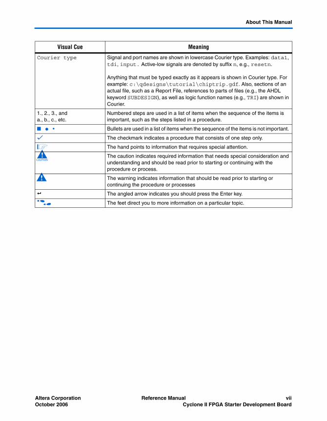
Visual Cue Meaning
Bold Type with Initial Capital Letters
Command names, dialog box titles, checkbox options, and dialog box options are shown in bold, initial capital letters. Example: Save As dialog box.
bold type External timing parameters, directory names, project names, disk drive names, filenames, filename extensions, and software utility names are shown in bold type. Examples: fMAX, \qdesigns directory, d: drive, chiptrip.gdf file.
Italic Type with Initial Capital Letters
Document titles are shown in italic type with initial capital letters. Example: AN 75: High-Speed Board Design.
Italic type Internal timing parameters and variables are shown in italic type. Examples: tPIA, n + 1.
Variable names are enclosed in angle brackets (< >) and shown in italic type. Example: <file name>, <project name>.pof file.
Initial Capital Letters Keyboard keys and menu names are shown with initial capital letters. Examples: Delete key, the Options menu.
“Subheading Title” References to sections within a document and titles of on-line help topics are shown in quotation marks. Example: “Typographic Conventions.”
vi Reference Manual Altera CorporationCyclone II FPGA Starter Development Board October 2006
About This Manual
Courier type Signal and port names are shown in lowercase Courier type. Examples: data1, tdi, input. Active-low signals are denoted by suffix n, e.g., resetn.
Anything that must be typed exactly as it appears is shown in Courier type. For example: c:\qdesigns\tutorial\chiptrip.gdf. Also, sections of an actual file, such as a Report File, references to parts of files (e.g., the AHDL keyword SUBDESIGN), as well as logic function names (e.g., TRI) are shown in Courier.
1., 2., 3., anda., b., c., etc.
Numbered steps are used in a list of items when the sequence of the items is important, such as the steps listed in a procedure.
■ ● • Bullets are used in a list of items when the sequence of the items is not important.
v The checkmark indicates a procedure that consists of one step only.
1 The hand points to information that requires special attention.
c The caution indicates required information that needs special consideration and understanding and should be read prior to starting or continuing with the procedure or process.
w The warning indicates information that should be read prior to starting or continuing the procedure or processes
r The angled arrow indicates you should press the Enter key.
f The feet direct you to more information on a particular topic.
Visual Cue Meaning
Altera Corporation Reference Manual viiOctober 2006 Cyclone II FPGA Starter Development Board

About This Manual
viii Reference Manual Altera CorporationCyclone II FPGA Starter Development Board October 2006
Altera Corporation October 2006
1. Introduction
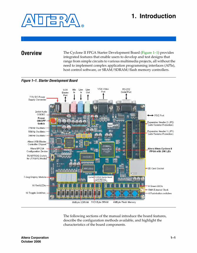
Overview The Cyclone II FPGA Starter Development Board (Figure 1–1) provides integrated features that enable users to develop and test designs that range from simple circuits to various multimedia projects, all without the need to implement complex application programming interfaces (APIs), host control software, or SRAM/SDRAM/flash memory controllers.
Figure 1–1. Starter Development Board
The following sections of the manual introduce the board features, describe the configuration methods available, and highlight the characteristics of the board components.
1–1

Introduction
Hardware Features
The development board has the following hardware features:
■ Altera Cyclone® II EP2C20 FPGA device■ Altera EPCS4 Serial Configuration device■ USB-Blaster controller chip set for programming and user API
control, supporting both JTAG and Active Serial (AS) programming modes
■ 512-KByte SRAM■ 8-MByte SDRAM■ 4-MByte Flash memory■ SD Flash Card socket■ 4 Push button switches■ 10 Toggle switches■ 10 Red user LEDs■ 8 Green user LEDs■ 50 MHz, 27 MHz, and 24 MHz oscillators for clock sources■ 24-bit CD-quality audio CODEC with line-in, line-out, and
microphone-in jacks■ VGA DAC (4-bit resistor network) with VGA-out connector■ RS-232 transceiver and 9-pin connector■ PS/2 mouse/keyboard connector■ Two 40-pin expansion headers with resistor protection■ 7.5V DC adapter or a USB cable (provided in the kit) for power
Software Features
Flexible control of the development board and Altera hardware and software tools provide an effective FPGA-based design environment. In addition to the hardware features, the development board provides software support for standard I/O interfaces and a control panel facility for accessing various components. The kit also provides software for a number of demonstrations that illustrate the advanced capabilities of the development board.
Use of the development board requires familiarity with the Altera Quartus II software. Tutorials for the Quartus II software and for the Cyclone II FPGA Starter Board are available on the Altera web site or on the included development kit CD-ROM in the Examples directory.
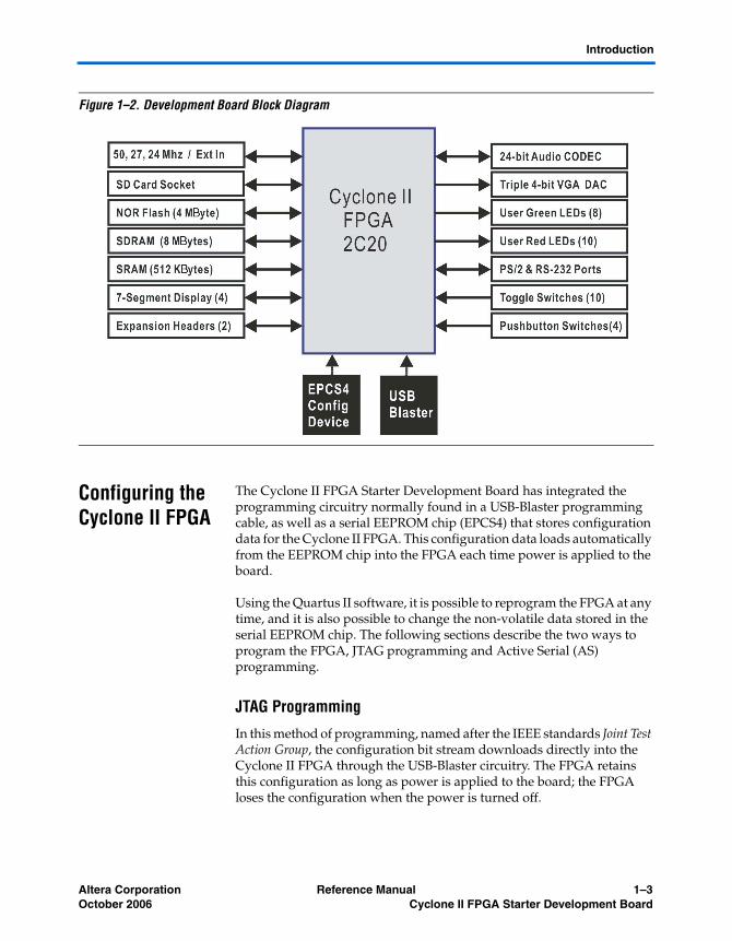
Block Diagram The block diagram of the development board (Figure 1–2) shows that for maximum user flexibility, all the blocks connect through the Cyclone II FPGA device. Thus, the user can implement any system design by configuring the FPGA.
1–2 Reference Manual Altera CorporationCyclone II FPGA Starter Development Board October 2006
Introduction
Figure 1–2. Development Board Block Diagram
Configuring the Cyclone II FPGA
The Cyclone II FPGA Starter Development Board has integrated the programming circuitry normally found in a USB-Blaster programming cable, as well as a serial EEPROM chip (EPCS4) that stores configuration data for the Cyclone II FPGA. This configuration data loads automatically from the EEPROM chip into the FPGA each time power is applied to the board.
Using the Quartus II software, it is possible to reprogram the FPGA at any time, and it is also possible to change the non-volatile data stored in the serial EEPROM chip. The following sections describe the two ways to program the FPGA, JTAG programming and Active Serial (AS) programming.
JTAG Programming
In this method of programming, named after the IEEE standards Joint Test Action Group, the configuration bit stream downloads directly into the Cyclone II FPGA through the USB-Blaster circuitry. The FPGA retains this configuration as long as power is applied to the board; the FPGA loses the configuration when the power is turned off.
Altera Corporation Reference Manual 1–3October 2006 Cyclone II FPGA Starter Development Board
Introduction
f For detailed information about the USB-Blaster circuitry, refer to the Cyclone II FPGA Starter Board schematic found in the BoardDesignFiles / Schematic directory in the kit installation directory.
AS Programming
In the Active Serial programming method, the configuration bit stream downloads into the Altera EPCS4 serial EEPROM chip. The EEPROM provides non-volatile storage of the bit stream, retaining the information even when power to the Cyclone II FPGA Starter board is turned off. When the board powers up, the configuration data in the EPCS4 device automatically loads into the Cyclone II FPGA.
Configuration Procedure
For both the JTAG and AS programming methods, the Cyclone II FPGA Starter board connects to a host computer via a USB cable. Because of this connection type, the host computer identifies the board as an Altera USB-Blaster device. The following sections describe the JTAG and AS programming steps.
Configuring the FPGA in JTAG Mode
Figure 1–3 illustrates the JTAG configuration setup. To download a configuration bit stream into the Cyclone II FPGA, perform the following steps:
1. Ensure that power is applied to the Cyclone II FPGA Starter board.
2. Connect the supplied USB cable to the USB-Blaster port on the board.
3. Configure the JTAG programming circuit on the board by setting the RUN/PROG switch (on the left side of the board) to the RUN position.
4. To program the FPGA, use the Quartus II Programmer module to select a configuration bit-stream file with the .sof filename extension.
1–4 Reference Manual Altera CorporationCyclone II FPGA Starter Development Board October 2006

Introduction
Figure 1–3. JTAG Configuration Setup
Configuring the EPCS4 Device in AS Mode
Figure 1–4 illustrates the AS configuration setup. To download a configuration bit stream into the EPCS4 serial EEPROM device, perform the following steps:
1. Ensure that power is applied to the Cyclone II FPGA Starter board.
2. Connect the supplied USB cable to the USB-Blaster port on the board.
3. Configure the JTAG programming circuit by setting the RUN/PROG switch (on the left side of the board) to the PROG position.
4. To program the EPCS4 device, use the Quartus II Programmer module to select a configuration bit-stream file with the .pof filename extension.
5. After the programming operation completes, set the RUN/PROG switch back to the RUN position.
6. Reset the board by turning the power switch off and then on again. This action causes the new configuration data in the EPCS4 device to load into the FPGA chip.
f Refer to the Serial Configuration Devices chapter in the Altera Configuration Device Handbook for more information about the EPCS4 device.
USB Blaster Circuit
MAX 3128
USB
FPGA
JTAG Config Port
EPCS Serial Configuration
Device
RUN/PROG
RUN”
Auto Power on Config
Altera Corporation Reference Manual 1–5October 2006 Cyclone II FPGA Starter Development Board

Introduction
Figure 1–4. AS Configuration Setup
Component Summary
Table 1–1 lists the components, their locations, and brief descriptions.
USB Blaster Circuit
MAX 3128
USB
FPGA
JTAG Config Port
EPCS Serial Configuration
Device
RUN/PROG
PROG”
Auto Power on Config
Table 1–1. Cyclone II FPGA Development Board Components & Interfaces (Part 1 of 2)
Board Designation Name Description
U2 Cyclone II FPGA EP2C20 device
User Interface
KEY0 – KEY3 Push-button switches Four momentary contact switches for user input to the FPGA
SW0 – SW9 Toggle switches Ten toggle switches for configuration of the FPGA
LEDG0 – LEDG7 Individual LEDs Eight green LEDs driven by the FPGA
LEDR0 – LEDR9 Individual LEDs Ten red LEDs driven by the FPGA
HEX0 – HEX3 Seven-segment LEDs Four seven-segment LEDs that display numeric output from the FPGA
Memory
U7 SRAM memory 512 KBytes of SRAM
U9 Flash memory 4 MBytes of nonvolatile memory for use by both the FPGA and the configuration controller. LED7 lights whenever the flash chip-enable asserts.
U6 DDR SDRAM memory 8 MBytes of DDR SDRAM.
Connections & Interfaces
PS2KB PS/2 connector PS/2 keyboard connector
1–6 Reference Manual Altera CorporationCyclone II FPGA Starter Development Board October 2006

Introduction
Component Features
This section summarizes characteristics of each board component. For detailed descriptions, refer to Chapter 2, Development Board Components.
Cyclone II EP2C20 FPGA
■ 18,752 LEs■ 52 M4K RAM blocks■ 240K total RAM bits■ 26 embedded multipliers■ 4 PLLs■ 315 user I/O pins
RS232 Serial connector RS-232 9-pin serial connector with 5 V-tolerant buffers. Supports all RS-232 signals.
JP1 Expansion header connector Expansion header 1 connecting to 40 I/O pins on the FPGA with resistor voltage protection
JP2 Expansion header connector Expansion header 2 connecting to 40 I/O pins on the FPGA with resistor voltage protection
MIC Microphone input Audio CODEC connectors
LINEIN Audio Line input
LINEOUT Audio line output
VGA VGA connector VGA video port
SD CARD SD card socket Secure Data card socket
BLASTER JTAG connector USB Blaster Port JTAG connection to the MAX® configuration controller
Configuration & Reset
U16 Serial configuration device Altera EPCS4 low-cost serial configuration device to configure the FPGA
SW11 Power ON/OFF switch Push-button switch to power up the board
Clock Circuitry
Y1 Oscillator 50 MHz clock signal driven to FPGA
Y2 Oscillator 27 MHz clock signal driven to FPGA
Y3 Oscillator 24 MHz clock signal driven to FPGA
EXT_CLOCK External clock input Connector to FPGA clock pin
Power Supply
DC7.5V DC power jack 7.5 V DC unregulated power source
Table 1–1. Cyclone II FPGA Development Board Components & Interfaces (Part 2 of 2)
Board Designation Name Description
Altera Corporation Reference Manual 1–7October 2006 Cyclone II FPGA Starter Development Board

Introduction
■ FineLine BGA 484-pin package
Serial Configuration Device and USB Blaster Circuit
■ Altera EPCS4 serial configuration device■ On-board USB-Blaster chip set for programming
and user API control■ Selectable JTAG and AS programming modes
SRAM
■ 512-KByte static RAM memory chip■ Organized as 256K x 16 bits■ Accessible as memory for the Nios II processor
and by the Control Panel GUI
SDRAM
■ 8-MByte single data rate synchronous dynamic RAM memory chip■ Organized as 1M x 16 bits x 4 banks■ Accessible as memory for the Nios II processor
and by the Control Panel GUI
Flash Memory
■ 4-MByte NOR flash memory■ 8-bit data bus■ Accessible as memory for the Nios II processor
and by the Control Panel GUI
SD Card Socket
■ Provides SPI mode for SD card access■ Accessible as memory for the Nios II processor
with the DE1 SD Card Driver
Push Button Switches
■ 4 push button switches■ Debounced by a Schmitt trigger circuit■ Normally HIGH; generates one active-LOW pulse
when the switch is pressed
Toggle Switches
■ 10 toggle switches for user inputs
1–8 Reference Manual Altera CorporationCyclone II FPGA Starter Development Board October 2006
Introduction
■ A switch produces logic 0 when in the DOWN(closest to the edge of the board) positionand logic 1 when in the UP position
Clock Inputs
■ 50-MHz oscillator ■ 27-MHz oscillator■ 24-MHz oscillator■ SMA external clock input
Audio CODEC
■ Wolfson WM8731 24-bit sigma-delta audio CODEC■ Line-level input, line-level output, and microphone input jacks■ Sampling frequency: 8 to 96 KHz■ Applications for MP3 players and recorders, PDAs,
smart phones, voice recorders
VGA Output
■ Uses a 4-bit resistor-network DAC ■ 15-pin high-density D-sub connector■ Supports up to 640x480 at 60-Hz refresh rate ■ Can be used with the Cyclone II FPGA to implement
a high-performance TV encoder
Serial Ports
■ One RS-232 port■ One PS/2 port■ DB-9 serial connector for the RS-232 port■ PS/2 connector for connecting a PS2 mouse
or keyboard to the board
Dual 40-Pin Expansion Headers
■ 72 Cyclone II I/O pins and 8 power and ground linesconnect to two, 40-pin expansion connectors
■ 40-Pin header designed to accept a standard 40-pinribbon cable used for IDE hard drives
■ Resistor protection provided
Altera Corporation Reference Manual 1–9October 2006 Cyclone II FPGA Starter Development Board
Introduction
1–10 Reference Manual Altera CorporationCyclone II FPGA Starter Development Board October 2006
Altera Corporation October 2006
2. Development BoardComponents
Component List The development board comprises the following major components:
■ Altera Cyclone II EP2C20 FPGA■ Altera USB-Blaster controller chip set■ Altera EPCS4 configuration device■ VGA DAC■ 24-bit Audio CODEC■ Memory
● 8 MByte SDRAM● 512 KByte SRAM● 4 MByte flash memory
■ Internal dual clock circuit■ Switches
● Power ON/OFF switch● RUN/PROG mode selector switch● 4 momentary push button switches● 10 sliding toggle switches
■ Displays● LEDs: 8 green, 10 red● 4 seven-segment displays
■ Connectors● USB-Blaster port● Two, 40-pin expansion headers● SD card connector● RS-232 serial port● PS/2 port● VGA video port● Audio microphone-in, line-in, line-out ports● SMA external clock connector● 7.5 V power supply connector
Cyclone II EP2C20 FPGA
The main device that defines the starter development board is an Altera Cyclone II EP2C20 FPGA in a 484-pin FineLine BGA® package. Table 2–1 lists the FPGA features.
Table 2–1. Cyclone II EP2C20 FPGA Features (Part 1 of 2)
LEs 18,752
M4K Memory Blocks 52
2–1

Development Board Components
f For Cyclone II-related documentation including pin out data for the EP2C20 device, refer to the Altera Cyclone II literature page at www.altera.com/literature/lit-cyc2.jsp.
USB-Blaster Controller
The Cyclone II FPGA Starter Development Board includes an integrated USB-Blaster controller. Accessed across a USB-Blaster cable connection by Altera USB-Blaster driver software on a host computer, the USB-Blaster controller enables direct programming of the FPGA.
f Refer to ((section on Configuring the FPGA)) and the Cyclone II FPGA Starter Development Kit User Guide for further details on configuring the FPGA.
EPCS4 The Cyclone II FPGA Starter Development Board includes a serial EPCS4 EEPROM chip that stores configuration data for the Cyclone II FPGA. The EPCS4 device automatically loads stored configuration data into the FPGA each time power is applied to the board.
Quartus II software on a host computer connected to the board across a USB-Blaster cable and controller can change the non-volatile data stored in the serial EEPROM chip. The EPCS4 device can store FPGA configuration data, or program data, or both.
f Refer to “Configuring the Cyclone II FPGA” on page 1–3 and the Cyclone II FPGA Starter Development Kit User Guide for further details on configuring the FPGA. Refer to the Serial Configuration Devices chapter in the Altera Configuration Device Handbook for more information about the EPCS4 device.
VGA DAC The development board includes a 4-bit VGA digital-to-analog converter (DAC) that can produce standard VGA output with a resolution of 640x480 pixels at 25 MHz. With the VGA DAC able to support a refresh rate up to 100 MHz, a user can implement a high-performance TV Encoder on the FPGA.
Total RAM Bits 240K
Embedded 18x18 Multiplier Blocks 26
PLLs 4
User I/O Pins 315
Table 2–1. Cyclone II EP2C20 FPGA Features (Part 2 of 2)
2–2 Reference Manual Altera CorporationCyclone II FPGA Starter Development Board October 2006

Development Board Components
The FPGA provides the synchronization signals directly to the VGA port, a16-pin D-SUB connector, VGA, located at the top edge of the board, while the DAC, using a resistor network, produces the red, green, and blue (RGB) analog data signals.
VGA Timing
Figure 2–1 illustrates the basic timing requirements for each horizontal line, or row, displayed on a VGA monitor. An active-LOW pulse of time duration a (Table 2–2) applied to the horizontal synchronization input, hsync, of the monitor marks the end of one row of data and the start of the next. After the hsync pulse, the RGB data inputs on the monitor must be off, driven to 0 volts, for a backporch time period b.
Figure 2–1. VGA Horizontal Timing
The display interval starts after the backporch time period b expires. For a time duration c, the RGB data inputs turn on and RGB data drives each pixel in turn across the row. After the display completes, the RGB data inputs must again turn off for a frontporch period d before the next hsync pulse restarts the process on the next row.
The vertical synchronization timing resembles the diagram in Figure 2–1, except a vsync pulse marks the end of one frame and the start of the next, and the data display refers to the set of rows in the frame.
Table 2–2 lists the VGA horizontal timing specifications.
Table 2–2. VGA Horizontal Timing Specifications
Configuration Resolution (HxV) a (μs) b (μs) c (μs) d (μs) Pixel clock (MHz)
VGA (60 Hz) 640 x 480 3.8 1.9 25.4 0.6 25 (640/c)
Altera Corporation Reference Manual 2–3October 2006 Cyclone II FPGA Starter Development Board
Development Board Components
Table 2–3 lists the VGA vertical timing specifications.
VGA Circuit Pin List
Table 2–4 lists the FPGA pins assigned to the VGA circuit.
VGA Circuit Schematic
Figure 2–2 shows the VGA circuit schematic.
Table 2–3. VGA Vertical Timing Specifications
Configuration Resolution (HxV) a (lines) b (lines) c (lines) d (lines)
VGA (60 Hz) 640 x 480 2 33 480 10
Table 2–4. VGA Circuit FPGA Pin Connections
Signal Name FPGA Pin Description
VGA_R[0] PIN_D9 VGA Red[0]
VGA_R[1] PIN_C9 VGA Red[1]
VGA_R[2] PIN_A7 VGA Red[2]
VGA_R[3] PIN_B7 VGA Red[3]
VGA_G[0] PIN_B8 VGA Green[0]
VGA_G[1] PIN_C10 VGA Green[1]
VGA_G[2] PIN_B9 VGA Green[2]
VGA_G[3] PIN_A8 VGA Green[3]
VGA_B[0] PIN_A9 VGA Blue[0]
VGA_B[1] PIN_D11 VGA Blue[1]
VGA_B[2] PIN_A10 VGA Blue[2]
VGA_B[3] PIN_B10 VGA Blue[3]
VGA_HS PIN_A11 VGA H_SYNC
VGA_VS PIN_B11 VGA V_SYNC
2–4 Reference Manual Altera CorporationCyclone II FPGA Starter Development Board October 2006
Development Board Components
Figure 2–2. VGA Circuit Schematic Diagram
Audio CODEC The development board provides a Wolfson WM8731high-quality, 24-bit, sigma-delta audio encoder/decoder (CODEC) for applications such as MP3 players and recorders, PDAs, smart phones, and voice recorders.
Altera Corporation Reference Manual 2–5October 2006 Cyclone II FPGA Starter Development Board

Development Board Components
This device features microphone-in, line-in, and line-out ports, with a sample rate adjustable from 8 kHz to 96 kHz. A serial I2C bus interface connected to FPGA pins controls the WM8731 CODEC.
f For information about the WM8731 CODEC, refer to the BoardDesignFiles\Datasheet folder in the kit installation directory or to the manufacturer's web site.
Audio Circuit Schematic
Figure 2–3 shows the audio circuit schematic.
Figure 2–3. Audio Circuit Schematic Diagram
2–6 Reference Manual Altera CorporationCyclone II FPGA Starter Development Board October 2006

Development Board Components
Audio Circuit Pin List
Table 2–5 lists the FPGA pins assigned to the audio circuit.
Memory The development board provides three types of memory:
■ An 8-MByte SDRAM■ A 512-KByte SRAM■ A 4-MByte flash memory
f For information on the memory devices, refer to the BoardDesignFiles\Datasheet folder in the kit installation directory.
SDRAM Schematic and Pin List
Figure 2–4 shows the SDRAM interface signals.
Table 2–5. Audio Circuit FPGA Pin Connections
Signal Name FPGA Pin Description
AUD_ADCLRCK PIN_A6 Audio CODEC ADC LR Clock
AUD_ADCDAT PIN_B6 Audio CODEC ADC Data
AUD_DACLRCK PIN_A5 Audio CODEC DAC LR Clock
AUD_DACDAT PIN_B5 Audio CODEC DAC Data
AUD_XCK PIN_B4 Audio CODEC Chip Clock
AUD_BCLK PIN_A4 Audio CODEC Bit-Stream Clock
I2C_SCLK PIN_A3 I2C Data
I2C_SDAT PIN_B3 I2C Clock
Altera Corporation Reference Manual 2–7October 2006 Cyclone II FPGA Starter Development Board

Development Board Components
Figure 2–4. SDRAM Interface Connections Diagram
Table 2–6 lists the FPGA pins assigned to the SDRAM.
Table 2–6. SDRAM FPGA Pin Connections (Part 1 of 2)
Signal Name FPGA Pin Description
DRAM_ADDR[0] PIN_W4 SDRAM Address[0]
DRAM_ADDR[1] PIN_W5 SDRAM Address[1]
DRAM_ADDR[2] PIN_Y3 SDRAM Address[2]
DRAM_ADDR[3] PIN_Y4 SDRAM Address[3]
DRAM_ADDR[4] PIN_R6 SDRAM Address[4]
DRAM_ADDR[5] PIN_R5 SDRAM Address[5]
DRAM_ADDR[6] PIN_P6 SDRAM Address[6]
2–8 Reference Manual Altera CorporationCyclone II FPGA Starter Development Board October 2006
Development Board Components
SRAM Schematic and Pin List
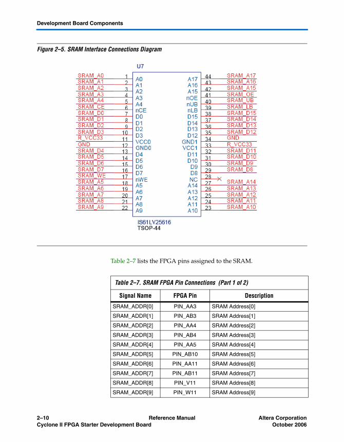
Figure 2–5 shows the SRAM interface signals.
DRAM_ADDR[7] PIN_P5 SDRAM Address[7]
DRAM_ADDR[8] PIN_P3 SDRAM Address[8]
DRAM_ADDR[9] PIN_N4 SDRAM Address[9]
DRAM_ADDR[10] PIN_W3 SDRAM Address[10]
DRAM_ADDR[11] PIN_N6 SDRAM Address[11]
DRAM_DQ[0] PIN_U1 SDRAM Data[0]
DRAM_DQ[1] PIN_U2 SDRAM Data[1]
DRAM_DQ[2] PIN_V1 SDRAM Data[2]
DRAM_DQ[3] PIN_V2 SDRAM Data[3]
DRAM_DQ[4] PIN_W1 SDRAM Data[4]
DRAM_DQ[5] PIN_W2 SDRAM Data[5]
DRAM_DQ[6] PIN_Y1 SDRAM Data[6]
DRAM_DQ[7] PIN_Y2 SDRAM Data[7]
DRAM_DQ[8] PIN_N1 SDRAM Data[8]
DRAM_DQ[9] PIN_N2 SDRAM Data[9]
DRAM_DQ[10] PIN_P1 SDRAM Data[10]
DRAM_DQ[11] PIN_P2 SDRAM Data[11]
DRAM_DQ[12] PIN_R1 SDRAM Data[12]
DRAM_DQ[13] PIN_R2 SDRAM Data[13]
DRAM_DQ[14] PIN_T1 SDRAM Data[14]
DRAM_DQ[15] PIN_T2 SDRAM Data[15]
DRAM_BA_0 PIN_U3 SDRAM Bank Address[0]
DRAM_BA_1 PIN_V4 SDRAM Bank Address[1]
DRAM_LDQM PIN_R7 SDRAM Low-byte Data Mask
DRAM_UDQM PIN_M5 SDRAM High-byte Data Mask
DRAM_RAS_N PIN_T5 SDRAM Row Address Strobe
DRAM_CAS_N PIN_T3 SDRAM Column Address Strobe
DRAM_CKE PIN_N3 SDRAM Clock Enable
DRAM_CLK PIN_U4 SDRAM Clock
DRAM_WE_N PIN_R8 SDRAM Write Enable
DRAM_CS_N PIN_T6 SDRAM Chip Select
Table 2–6. SDRAM FPGA Pin Connections (Part 2 of 2)
Signal Name FPGA Pin Description
Altera Corporation Reference Manual 2–9October 2006 Cyclone II FPGA Starter Development Board
Development Board Components
Figure 2–5. SRAM Interface Connections Diagram
Table 2–7 lists the FPGA pins assigned to the SRAM.
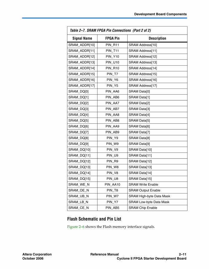
Table 2–7. SRAM FPGA Pin Connections (Part 1 of 2)
Signal Name FPGA Pin Description
SRAM_ADDR[0] PIN_AA3 SRAM Address[0]
SRAM_ADDR[1] PIN_AB3 SRAM Address[1]
SRAM_ADDR[2] PIN_AA4 SRAM Address[2]
SRAM_ADDR[3] PIN_AB4 SRAM Address[3]
SRAM_ADDR[4] PIN_AA5 SRAM Address[4]
SRAM_ADDR[5] PIN_AB10 SRAM Address[5]
SRAM_ADDR[6] PIN_AA11 SRAM Address[6]
SRAM_ADDR[7] PIN_AB11 SRAM Address[7]
SRAM_ADDR[8] PIN_V11 SRAM Address[8]
SRAM_ADDR[9] PIN_W11 SRAM Address[9]
2–10 Reference Manual Altera CorporationCyclone II FPGA Starter Development Board October 2006
Development Board Components
Flash Schematic and Pin List
Figure 2–6 shows the Flash memory interface signals.
SRAM_ADDR[10] PIN_R11 SRAM Address[10]
SRAM_ADDR[11] PIN_T11 SRAM Address[11]
SRAM_ADDR[12] PIN_Y10 SRAM Address[12]
SRAM_ADDR[13] PIN_U10 SRAM Address[13]
SRAM_ADDR[14] PIN_R10 SRAM Address[14]
SRAM_ADDR[15] PIN_T7 SRAM Address[15]
SRAM_ADDR[16] PIN_Y6 SRAM Address[16]
SRAM_ADDR[17] PIN_Y5 SRAM Address[17]
SRAM_DQ[0] PIN_AA6 SRAM Data[0]
SRAM_DQ[1] PIN_AB6 SRAM Data[1]
SRAM_DQ[2] PIN_AA7 SRAM Data[2]
SRAM_DQ[3] PIN_AB7 SRAM Data[3]
SRAM_DQ[4] PIN_AA8 SRAM Data[4]
SRAM_DQ[5] PIN_AB8 SRAM Data[5]
SRAM_DQ[6] PIN_AA9 SRAM Data[6]
SRAM_DQ[7] PIN_AB9 SRAM Data[7]
SRAM_DQ[8] PIN_Y9 SRAM Data[8]
SRAM_DQ[9] PIN_W9 SRAM Data[9]
SRAM_DQ[10] PIN_V9 SRAM Data[10]
SRAM_DQ[11] PIN_U9 SRAM Data[11]
SRAM_DQ[12] PIN_R9 SRAM Data[12]
SRAM_DQ[13] PIN_W8 SRAM Data[13]
SRAM_DQ[14] PIN_V8 SRAM Data[14]
SRAM_DQ[15] PIN_U8 SRAM Data[15]
SRAM_WE_N PIN_AA10 SRAM Write Enable
SRAM_OE_N PIN_T8 SRAM Output Enable
SRAM_UB_N PIN_W7 SRAM High-byte Data Mask
SRAM_LB_N PIN_Y7 SRAM Low-byte Data Mask
SRAM_CE_N PIN_AB5 SRAM Chip Enable
Table 2–7. SRAM FPGA Pin Connections (Part 2 of 2)
Signal Name FPGA Pin Description
Altera Corporation Reference Manual 2–11October 2006 Cyclone II FPGA Starter Development Board

Development Board Components
Figure 2–6. Flash Memory Interface Connections Diagram
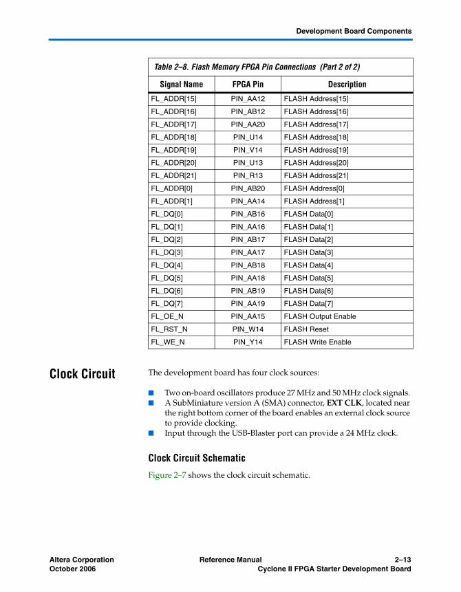
Table 2–8 lists the FPGA pins assigned to the flash memory.
Table 2–8. Flash Memory FPGA Pin Connections (Part 1 of 2)
Signal Name FPGA Pin Description
FL_ADDR[0] PIN_AB20 FLASH Address[0]
FL_ADDR[1] PIN_AA14 FLASH Address[1]
FL_ADDR[2] PIN_Y16 FLASH Address[2]
FL_ADDR[3] PIN_R15 FLASH Address[3]
FL_ADDR[4] PIN_T15 FLASH Address[4]
FL_ADDR[5] PIN_U15 FLASH Address[5]
FL_ADDR[6] PIN_V15 FLASH Address[6]
FL_ADDR[7] PIN_W15 FLASH Address[7]
FL_ADDR[8] PIN_R14 FLASH Address[8]
FL_ADDR[9] PIN_Y13 FLASH Address[9]
FL_ADDR[10] PIN_R12 FLASH Address[10]
FL_ADDR[11] PIN_T12 FLASH Address[11]
FL_ADDR[12] PIN_AB14 FLASH Address[12]
FL_ADDR[13] PIN_AA13 FLASH Address[13]
FL_ADDR[14] PIN_AB13 FLASH Address[14]
2–12 Reference Manual Altera CorporationCyclone II FPGA Starter Development Board October 2006
Development Board Components
Clock Circuit The development board has four clock sources:
■ Two on-board oscillators produce 27 MHz and 50 MHz clock signals. ■ A SubMiniature version A (SMA) connector, EXT CLK, located near
the right bottom corner of the board enables an external clock source to provide clocking.
■ Input through the USB-Blaster port can provide a 24 MHz clock.
Clock Circuit Schematic
Figure 2–7 shows the clock circuit schematic.
FL_ADDR[15] PIN_AA12 FLASH Address[15]
FL_ADDR[16] PIN_AB12 FLASH Address[16]
FL_ADDR[17] PIN_AA20 FLASH Address[17]
FL_ADDR[18] PIN_U14 FLASH Address[18]
FL_ADDR[19] PIN_V14 FLASH Address[19]
FL_ADDR[20] PIN_U13 FLASH Address[20]
FL_ADDR[21] PIN_R13 FLASH Address[21]
FL_ADDR[0] PIN_AB20 FLASH Address[0]
FL_ADDR[1] PIN_AA14 FLASH Address[1]
FL_DQ[0] PIN_AB16 FLASH Data[0]
FL_DQ[1] PIN_AA16 FLASH Data[1]
FL_DQ[2] PIN_AB17 FLASH Data[2]
FL_DQ[3] PIN_AA17 FLASH Data[3]
FL_DQ[4] PIN_AB18 FLASH Data[4]
FL_DQ[5] PIN_AA18 FLASH Data[5]
FL_DQ[6] PIN_AB19 FLASH Data[6]
FL_DQ[7] PIN_AA19 FLASH Data[7]
FL_OE_N PIN_AA15 FLASH Output Enable
FL_RST_N PIN_W14 FLASH Reset
FL_WE_N PIN_Y14 FLASH Write Enable
Table 2–8. Flash Memory FPGA Pin Connections (Part 2 of 2)
Signal Name FPGA Pin Description
Altera Corporation Reference Manual 2–13October 2006 Cyclone II FPGA Starter Development Board
Development Board Components
Figure 2–7. Clocking Circuit Schematic Diagram
Clock Input Pin List
Table 2–9 lists the FPGA pins assigned to the display segments.
Switches The development board provides the following user switches:
■ Power ON/OFF switch■ RUN/PROG switch■ 4 push button switches■ 10 Toggle switches
Table 2–9. Clock Circuit FPGA Pin Connections
Signal Name FPGA Pin Description
CLOCK_27 PIN_D12 27 MHz clock input
CLOCK_50 PIN_L1 50 MHz clock input
CLOCK_24 PIN_B12 24 MHz clock input from USB Blaster
EXT_CLOCK PIN_M21 External (SMA) clock input
2–14 Reference Manual Altera CorporationCyclone II FPGA Starter Development Board October 2006

Development Board Components
Power ON/OFF Switch
The Cyclone II FPGA Starter board receives its power from either the USB port directly or the included 7.5V power adapter. The Power On/Off switch gates the power from both of these sources to the rest of the board.
RUN/PROG Switch
The RUN/PROG switch directs the JTAG signals from the USB-Blaster circuit to the FPGA directly when in the RUN position (Figure 2–8) or to the EPCS4 Serial EEPROM configuration device when in the PROG position (Figure 2–9).
Figure 2–8. RUN/PROG Switch in RUN Position
Figure 2–9. RUN/PROG Switch in PROG Position
With the RUN/PROG switch in the RUN position, the FPGA configures from the EPCS4 device on power up.
USB Blaster Circuit
MAX 3128
USB
FPGA
JTAG Config Port
EPCS Serial Configuration
Device
RUN/PROG
RUN”
Auto Power on Config
USB Blaster Circuit
MAX 3128
USB
FPGA
JTAG Config Port
EPCS Serial Configuration
Device
RUN/PROG
PROG”
Auto Power on Config
Altera Corporation Reference Manual 2–15October 2006 Cyclone II FPGA Starter Development Board
Development Board Components
Additionally, with the switch in the RUN position, the Quartus II Programmer can program the FPGA directly through the USB Blaster circuit. With the switch in the PROG position, the Quartus II Programmer can program the EPCS4 device.
Push Button Switches
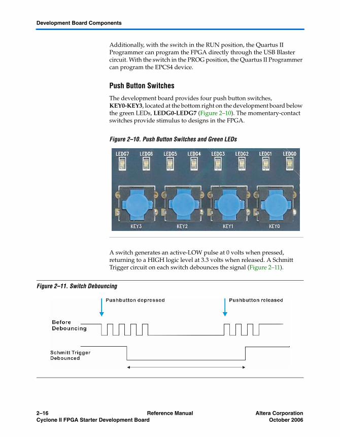
The development board provides four push button switches, KEY0-KEY3, located at the bottom right on the development board below the green LEDs, LEDG0-LEDG7 (Figure 2–10). The momentary-contact switches provide stimulus to designs in the FPGA.
Figure 2–10. Push Button Switches and Green LEDs
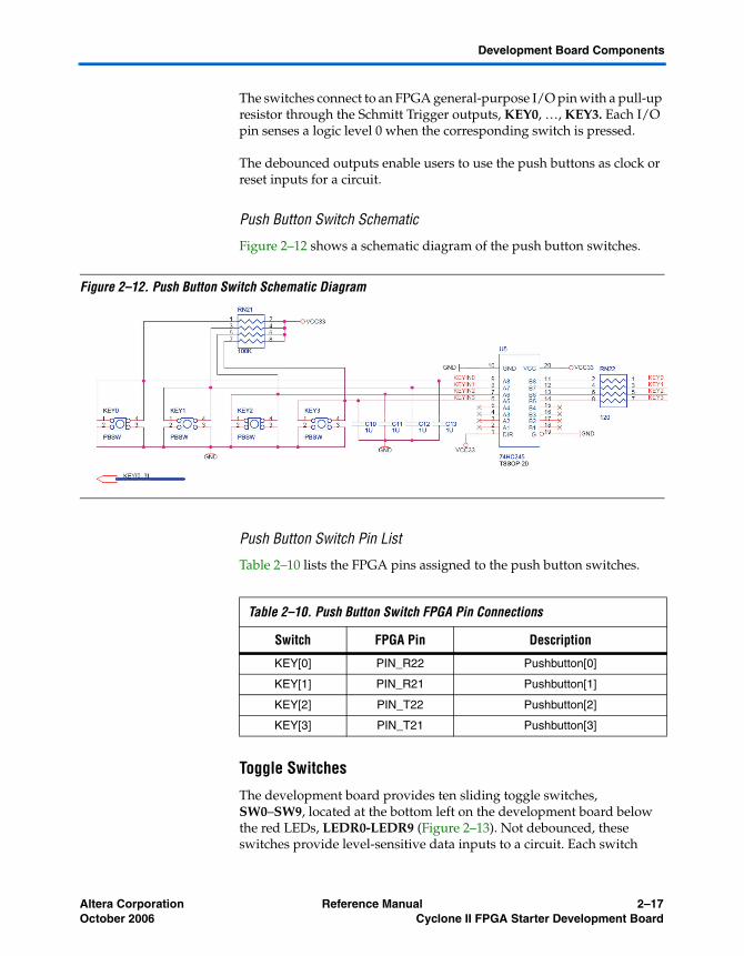
A switch generates an active-LOW pulse at 0 volts when pressed, returning to a HIGH logic level at 3.3 volts when released. A Schmitt Trigger circuit on each switch debounces the signal (Figure 2–11).
Figure 2–11. Switch Debouncing
2–16 Reference Manual Altera CorporationCyclone II FPGA Starter Development Board October 2006
Development Board Components
The switches connect to an FPGA general-purpose I/O pin with a pull-up resistor through the Schmitt Trigger outputs, KEY0, …, KEY3. Each I/O pin senses a logic level 0 when the corresponding switch is pressed.
The debounced outputs enable users to use the push buttons as clock or reset inputs for a circuit.
Push Button Switch Schematic
Figure 2–12 shows a schematic diagram of the push button switches.
Figure 2–12. Push Button Switch Schematic Diagram
Push Button Switch Pin List
Table 2–10 lists the FPGA pins assigned to the push button switches.
Toggle Switches
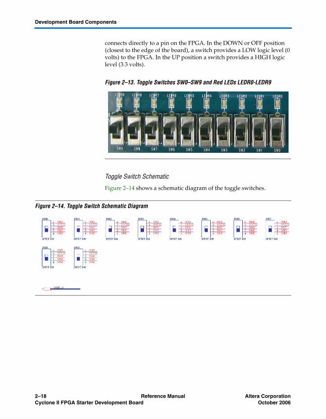
The development board provides ten sliding toggle switches, SW0–SW9, located at the bottom left on the development board below the red LEDs, LEDR0-LEDR9 (Figure 2–13). Not debounced, these switches provide level-sensitive data inputs to a circuit. Each switch
Table 2–10. Push Button Switch FPGA Pin Connections
Switch FPGA Pin Description
KEY[0] PIN_R22 Pushbutton[0]
KEY[1] PIN_R21 Pushbutton[1]
KEY[2] PIN_T22 Pushbutton[2]
KEY[3] PIN_T21 Pushbutton[3]
Altera Corporation Reference Manual 2–17October 2006 Cyclone II FPGA Starter Development Board
Development Board Components
connects directly to a pin on the FPGA. In the DOWN or OFF position (closest to the edge of the board), a switch provides a LOW logic level (0 volts) to the FPGA. In the UP position a switch provides a HIGH logic level (3.3 volts).
Figure 2–13. Toggle Switches SW0–SW9 and Red LEDs LEDR0-LEDR9
Toggle Switch Schematic
Figure 2–14 shows a schematic diagram of the toggle switches.
Figure 2–14. Toggle Switch Schematic Diagram
2–18 Reference Manual Altera CorporationCyclone II FPGA Starter Development Board October 2006

Development Board Components
Toggle Switch Pin List
Table 2–11 lists the FPGA pins assigned to the toggle switches.
Displays The development board provides the following displays:
■ LEDs■ Seven-segment displays
LEDs
The development board provides 18 user-controllable LEDs, 10 red LEDs, LEDR0–LEDR9, above the toggle switches (Figure 2–13) and 8 green LEDs, LEDG0–LEDG7, above the four push button switches (Figure 2–10). Each LED connects directly to an FPGA general purpose I/O pin. A HIGH logic level on a pin turns the LED on; a LOW logic level on a pin turns the LED off.
LED Schematic
Figure 2–15 shows a schematic diagram of the LEDs.
Table 2–11. Toggle Switch FPGA Pin Connections
Switch FPGA Pin Description
SW[0] PIN_L22 Toggle Switch[0]
SW[1] PIN_L21 Toggle Switch[1]
SW[2] PIN_M22 Toggle Switch[2]
SW[3] PIN_V12 Toggle Switch[3]
SW[4] PIN_W12 Toggle Switch[4]
SW[5] PIN_U12 Toggle Switch[5]
SW[6] PIN_U11 Toggle Switch[6]
SW[7] PIN_M2 Toggle Switch[7]
SW[8] PIN_M1 Toggle Switch[8]
SW[9] PIN_L2 Toggle Switch[9]
Altera Corporation Reference Manual 2–19October 2006 Cyclone II FPGA Starter Development Board

Development Board Components
Figure 2–15. LED Schematic Diagram
2–20 Reference Manual Altera CorporationCyclone II FPGA Starter Development Board October 2006
Development Board Components
LED Pin List
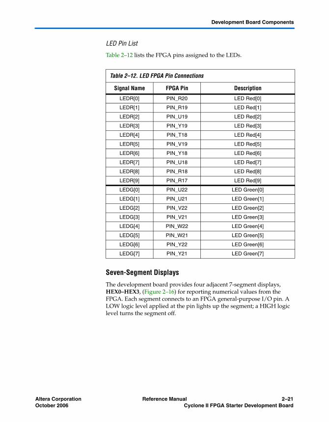
Table 2–12 lists the FPGA pins assigned to the LEDs.
Seven-Segment Displays
The development board provides four adjacent 7-segment displays, HEX0–HEX3, (Figure 2–16) for reporting numerical values from the FPGA. Each segment connects to an FPGA general-purpose I/O pin. A LOW logic level applied at the pin lights up the segment; a HIGH logic level turns the segment off.
Table 2–12. LED FPGA Pin Connections
Signal Name FPGA Pin Description
LEDR[0] PIN_R20 LED Red[0]
LEDR[1] PIN_R19 LED Red[1]
LEDR[2] PIN_U19 LED Red[2]
LEDR[3] PIN_Y19 LED Red[3]
LEDR[4] PIN_T18 LED Red[4]
LEDR[5] PIN_V19 LED Red[5]
LEDR[6] PIN_Y18 LED Red[6]
LEDR[7] PIN_U18 LED Red[7]
LEDR[8] PIN_R18 LED Red[8]
LEDR[9] PIN_R17 LED Red[9]
LEDG[0] PIN_U22 LED Green[0]
LEDG[1] PIN_U21 LED Green[1]
LEDG[2] PIN_V22 LED Green[2]
LEDG[3] PIN_V21 LED Green[3]
LEDG[4] PIN_W22 LED Green[4]
LEDG[5] PIN_W21 LED Green[5]
LEDG[6] PIN_Y22 LED Green[6]
LEDG[7] PIN_Y21 LED Green[7]
Altera Corporation Reference Manual 2–21October 2006 Cyclone II FPGA Starter Development Board

Development Board Components
Figure 2–16. Seven-Segment Displays
An index from 0 to 6 identifies each segment and its position (Figure 2–17). The development board does not connect or use the dot in the display.
Figure 2–17. Segment Index and Position
Seven-Segment Display Schematic
Figure 2–18 shows a schematic diagram of the LEDs.
2–22 Reference Manual Altera CorporationCyclone II FPGA Starter Development Board October 2006

Development Board Components
Figure 2–18. Seven-Segment Display Schematic Diagram
Seven-Segment Display Pin List
Table 2–13 lists the FPGA pins assigned to the display segments.
Table 2–13. Seven-Segment Display FPGA Pin Connections (Part 1 of 2)
Signal Name FPGA Pin Description
HEX0[0] PIN_J2 Seven-Segment segment 0[0]
HEX0[1] PIN_J1 Seven-Segment segment 0[1]
HEX0[2] PIN_H2 Seven-Segment segment 0[2]
HEX0[3] PIN_H1 Seven-Segment segment 0[3]
HEX0[4] PIN_F2 Seven-Segment segment 0[4]
HEX0[5] PIN_F1 Seven-Segment segment 0[5]
HEX0[6] PIN_E2 Seven-Segment segment 0[6]
HEX1[0] PIN_E1 Seven-Segment segment 1[0]
HEX1[1] PIN_H6 Seven-Segment segment 1[1]
Altera Corporation Reference Manual 2–23October 2006 Cyclone II FPGA Starter Development Board

Development Board Components
Connectors The development board provides the following connectors:
■ USB Type B connector port■ Expansion headers■ SD card connector■ RS-232 serial port■ PS/2 port■ VGA video port■ Audio microphone-in, line-in, line-out ports■ SMA external clock connector■ Power supply connector
HEX1[2] PIN_H5 Seven-Segment segment 1[2]
HEX1[3] PIN_H4 Seven-Segment segment 1[3]
HEX1[4] PIN_G3 Seven-Segment segment 1[4]
HEX1[5] PIN_D2 Seven-Segment segment 1[5]
HEX1[6] PIN_D1 Seven-Segment segment 1[6]
HEX2[0] PIN_G5 Seven-Segment segment 2[0]
HEX2[1] PIN_G6 Seven-Segment segment 2[1]
HEX2[2] PIN_C2 Seven-Segment segment 2[2]
HEX2[3] PIN_C1 Seven-Segment segment 2[3]
HEX2[4] PIN_E3 Seven-Segment segment 2[4]
HEX2[5] PIN_E4 Seven-Segment segment 2[5]
HEX2[6] PIN_D3 Seven-Segment segment 2[6]
HEX3[0] PIN_F4 Seven-Segment segment 3[0]
HEX3[1] PIN_D5 Seven-Segment segment 3[1]
HEX3[2] PIN_D6 Seven-Segment segment 3[2]
HEX3[3] PIN_J4 Seven-Segment segment 3[3]
HEX3[4] PIN_L8 Seven-Segment segment 3[4]
HEX3[5] PIN_F3 Seven-Segment segment 3[5]
HEX3[6] PIN_D4 Seven-Segment segment 3[6]
Table 2–13. Seven-Segment Display FPGA Pin Connections (Part 2 of 2)
Signal Name FPGA Pin Description
2–24 Reference Manual Altera CorporationCyclone II FPGA Starter Development Board October 2006

Development Board Components
USB-Blaster Port
The Cyclone II FPGA Starter Board includes USB-Blaster circuitry used for programming the FPGA or the EPCS4 device. A USB type B connector (Figure 2–19) provides the connection to this programming circuitry. Refer to“USB-Blaster Controller” on page 2–2 for more information about the USB Blaster circuitry.
Figure 2–19. USB Type B Connector
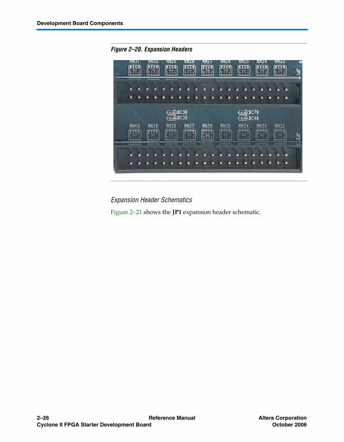
Expansion Headers
The development board provides two, 40-pin expansion headers, JP2, located on the right edge of the board, and JP1, located next to it (Figure 2–20). Each header connects directly to 36 pins on the FPGA, and also provides DC +5V (VCC5), DC +3.3V (VCC33), and two GND pins. Each pin on the expansion header connects to a resistor that provides protection from high and low voltages. The 40-pin header accepts a standard 40-pin ribbon cable used for IDE hard drives.
Altera Corporation Reference Manual 2–25October 2006 Cyclone II FPGA Starter Development Board
Development Board Components
Figure 2–20. Expansion Headers
Expansion Header Schematics
Figure 2–21 shows the JP1 expansion header schematic.
2–26 Reference Manual Altera CorporationCyclone II FPGA Starter Development Board October 2006

Development Board Components
Figure 2–21. Expansion Header JP1 Schematic Diagram
Figure 2–22 shows the JP2 expansion header schematic.
Altera Corporation Reference Manual 2–27October 2006 Cyclone II FPGA Starter Development Board

Development Board Components
Figure 2–22. Expansion Header JP2 Schematic Diagram
As examples, the figures show the protection circuitry for 4 of the pins on each header, but all 72 data pins include this circuitry. For complete information, refer to the schematic found in BoardDesignFiles\Schematic in the kit installation directory.
Expansion Header Pin List
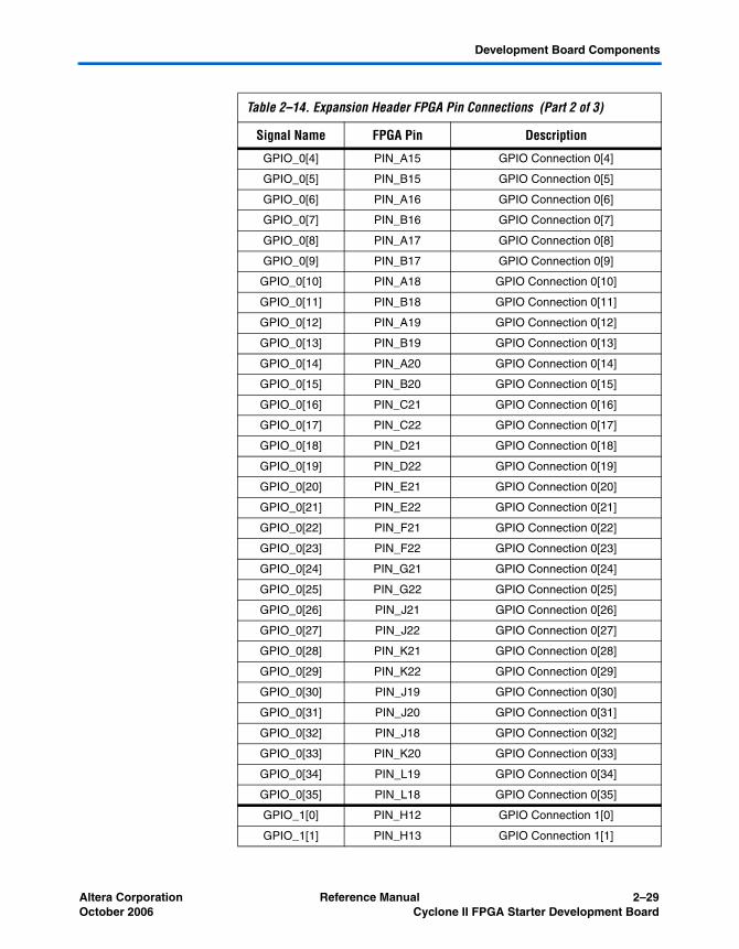
Table 2–14 lists the FPGA pins assigned to the expansion headers.
Table 2–14. Expansion Header FPGA Pin Connections (Part 1 of 3)
Signal Name FPGA Pin Description
GPIO_0[0] PIN_A13 GPIO Connection 0[0]
GPIO_0[1] PIN_B13 GPIO Connection 0[1]
GPIO_0[2] PIN_A14 GPIO Connection 0[2]
GPIO_0[3] PIN_B14 GPIO Connection 0[3]
2–28 Reference Manual Altera CorporationCyclone II FPGA Starter Development Board October 2006
Development Board Components
GPIO_0[4] PIN_A15 GPIO Connection 0[4]
GPIO_0[5] PIN_B15 GPIO Connection 0[5]
GPIO_0[6] PIN_A16 GPIO Connection 0[6]
GPIO_0[7] PIN_B16 GPIO Connection 0[7]
GPIO_0[8] PIN_A17 GPIO Connection 0[8]
GPIO_0[9] PIN_B17 GPIO Connection 0[9]
GPIO_0[10] PIN_A18 GPIO Connection 0[10]
GPIO_0[11] PIN_B18 GPIO Connection 0[11]
GPIO_0[12] PIN_A19 GPIO Connection 0[12]
GPIO_0[13] PIN_B19 GPIO Connection 0[13]
GPIO_0[14] PIN_A20 GPIO Connection 0[14]
GPIO_0[15] PIN_B20 GPIO Connection 0[15]
GPIO_0[16] PIN_C21 GPIO Connection 0[16]
GPIO_0[17] PIN_C22 GPIO Connection 0[17]
GPIO_0[18] PIN_D21 GPIO Connection 0[18]
GPIO_0[19] PIN_D22 GPIO Connection 0[19]
GPIO_0[20] PIN_E21 GPIO Connection 0[20]
GPIO_0[21] PIN_E22 GPIO Connection 0[21]
GPIO_0[22] PIN_F21 GPIO Connection 0[22]
GPIO_0[23] PIN_F22 GPIO Connection 0[23]
GPIO_0[24] PIN_G21 GPIO Connection 0[24]
GPIO_0[25] PIN_G22 GPIO Connection 0[25]
GPIO_0[26] PIN_J21 GPIO Connection 0[26]
GPIO_0[27] PIN_J22 GPIO Connection 0[27]
GPIO_0[28] PIN_K21 GPIO Connection 0[28]
GPIO_0[29] PIN_K22 GPIO Connection 0[29]
GPIO_0[30] PIN_J19 GPIO Connection 0[30]
GPIO_0[31] PIN_J20 GPIO Connection 0[31]
GPIO_0[32] PIN_J18 GPIO Connection 0[32]
GPIO_0[33] PIN_K20 GPIO Connection 0[33]
GPIO_0[34] PIN_L19 GPIO Connection 0[34]
GPIO_0[35] PIN_L18 GPIO Connection 0[35]
GPIO_1[0] PIN_H12 GPIO Connection 1[0]
GPIO_1[1] PIN_H13 GPIO Connection 1[1]
Table 2–14. Expansion Header FPGA Pin Connections (Part 2 of 3)
Signal Name FPGA Pin Description
Altera Corporation Reference Manual 2–29October 2006 Cyclone II FPGA Starter Development Board
Development Board Components
GPIO_1[2] PIN_H14 GPIO Connection 1[2]
GPIO_1[3] PIN_G15 GPIO Connection 1[3]
GPIO_1[4] PIN_E14 GPIO Connection 1[4]
GPIO_1[5] PIN_E15 GPIO Connection 1[5]
GPIO_1[6] PIN_F15 GPIO Connection 1[6]
GPIO_1[7] PIN_G16 GPIO Connection 1[7]
GPIO_1[8] PIN_F12 GPIO Connection 1[8]
GPIO_1[9] PIN_F13 GPIO Connection 1[9]
GPIO_1[10] PIN_C14 GPIO Connection 1[10]
GPIO_1[11] PIN_D14 GPIO Connection 1[11]
GPIO_1[12] PIN_D15 GPIO Connection 1[12]
GPIO_1[13] PIN_D16 GPIO Connection 1[13]
GPIO_1[14] PIN_C17 GPIO Connection 1[14]
GPIO_1[15] PIN_C18 GPIO Connection 1[15]
GPIO_1[16] PIN_C19 GPIO Connection 1[16]
GPIO_1[17] PIN_C20 GPIO Connection 1[17]
GPIO_1[18] PIN_D19 GPIO Connection 1[18]
GPIO_1[19] PIN_D20 GPIO Connection 1[19]
GPIO_1[20] PIN_E20 GPIO Connection 1[20]
GPIO_1[21] PIN_F20 GPIO Connection 1[21]
GPIO_1[22] PIN_E19 GPIO Connection 1[22]
GPIO_1[23] PIN_E18 GPIO Connection 1[23]
GPIO_1[24] PIN_G20 GPIO Connection 1[24]
GPIO_1[25] PIN_G18 GPIO Connection 1[25]
GPIO_1[26] PIN_G17 GPIO Connection 1[26]
GPIO_1[27] PIN_H17 GPIO Connection 1[27]
GPIO_1[28] PIN_J15 GPIO Connection 1[28]
GPIO_1[29] PIN_H18 GPIO Connection 1[29]
GPIO_1[30] PIN_N22 GPIO Connection 1[30]
GPIO_1[31] PIN_N21 GPIO Connection 1[31]
GPIO_1[32] PIN_P15 GPIO Connection 1[32]
GPIO_1[33] PIN_N15 GPIO Connection 1[33]
GPIO_1[34] PIN_P17 GPIO Connection 1[34]
GPIO_1[35] PIN_P18 GPIO Connection 1[35]
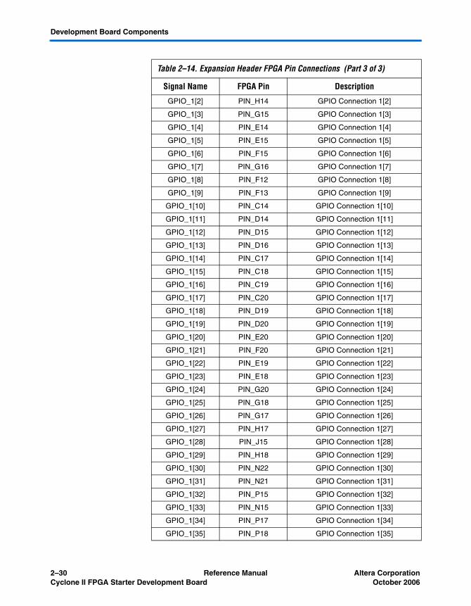
Table 2–14. Expansion Header FPGA Pin Connections (Part 3 of 3)
Signal Name FPGA Pin Description
2–30 Reference Manual Altera CorporationCyclone II FPGA Starter Development Board October 2006
Development Board Components
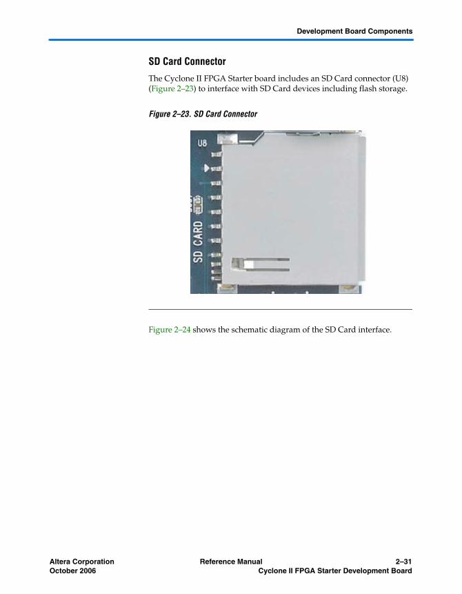
SD Card Connector
The Cyclone II FPGA Starter board includes an SD Card connector (U8) (Figure 2–23) to interface with SD Card devices including flash storage.
Figure 2–23. SD Card Connector
Figure 2–24 shows the schematic diagram of the SD Card interface.
Altera Corporation Reference Manual 2–31October 2006 Cyclone II FPGA Starter Development Board

Development Board Components
Figure 2–24. SD Card Interface Schematic
Table 2–15 lists the SD Card signal connections to FPGA pins.
RS-232 Serial Port
The development board uses a MAX232 transceiver chip and a 9-pin D-SUB connector (Figure 2–25) for RS-232 communications.
f For detailed information on how to use the transceiver, refer to the BoardDesignFiles\Datasheet folder in the kit installation directory or connect to the manufacturer’s web site.
Table 2–15. SD Card FPGA Connections
Signal Name FPGA Pin Description
SD_DAT W20 Data to/from SD Card
SD_DAT3 U20 SD Card Chip Select
SD_CMD Y20 Command line for SD Card
SD_CLK V20 SD Card Clock
2–32 Reference Manual Altera CorporationCyclone II FPGA Starter Development Board October 2006

Development Board Components
Figure 2–25. RS-232 Serial Connector
RS-232 Circuit Schematic
Figure 2–26 shows the RS-232 serial circuit schematic.
Figure 2–26. RS-232 Serial Circuit Schematic Diagram
Altera Corporation Reference Manual 2–33October 2006 Cyclone II FPGA Starter Development Board

Development Board Components
RS-232 Serial Circuit Pin List
Table 2–16 lists the FPGA pins assigned to the RS-232 serial circuit.
PS/2 Port
The development board includes a standard PS/2 interface and a connector for a PS/2 keyboard or mouse.
PS/2 Circuit Schematic
Figure 2–27 shows the PS/2 serial circuit schematic.
Figure 2–27. PS/2 Serial Circuit Schematic Diagram
PS/2 Serial Circuit Pin List
Table 2–17 lists the FPGA pins assigned to the PS/2 serial circuit.
Table 2–16. RS-232 Serial Circuit FPGA Pin Connections
Signal Name FPGA Pin Description
UART_RXD PIN_F14 UART Receiver
UART_TXD PIN_G12 UART Transmitter
Table 2–17. PS/2 Serial Circuit FPGA Pin Connections
Signal Name FPGA Pin Description
PS2_CLK PIN_H15 PS/2 Clock
PS2_DAT PIN_J14 PS/2 Data
2–34 Reference Manual Altera CorporationCyclone II FPGA Starter Development Board October 2006

Development Board Components
VGA Video Port
The Cyclone II FPGA Starter board includes a video connector (Figure 2–28) that connects to an on-board 4-bit video DAC. The connector is a standard DB15 15-pin analog VGA connector. Refer to “VGA DAC” on page 2–2 for a description of the circuitry attached to this connector.
Figure 2–28. VGA Connector
Audio Ports
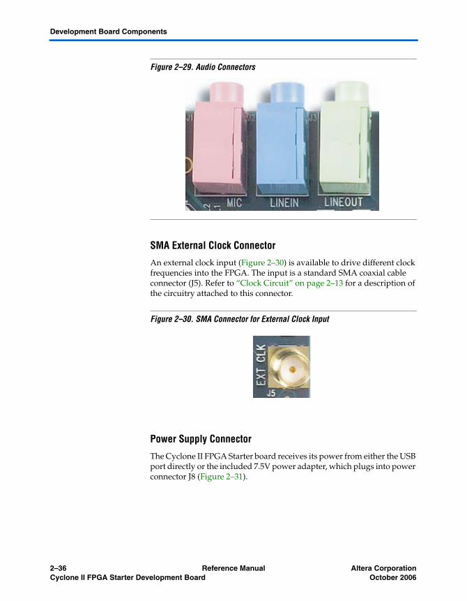
The audio circuit provides the following ports (Figure 2–29):
■ Microphone-in, MIC■ Line-in, LINEIN■ Line-out, LINEOUT
These are standard analog audio connectors. Refer to “Audio CODEC” on page 2–5 for a description of the circuitry attached to these connectors.
Altera Corporation Reference Manual 2–35October 2006 Cyclone II FPGA Starter Development Board
Development Board Components
Figure 2–29. Audio Connectors
SMA External Clock Connector
An external clock input (Figure 2–30) is available to drive different clock frequencies into the FPGA. The input is a standard SMA coaxial cable connector (J5). Refer to “Clock Circuit” on page 2–13 for a description of the circuitry attached to this connector.
Figure 2–30. SMA Connector for External Clock Input
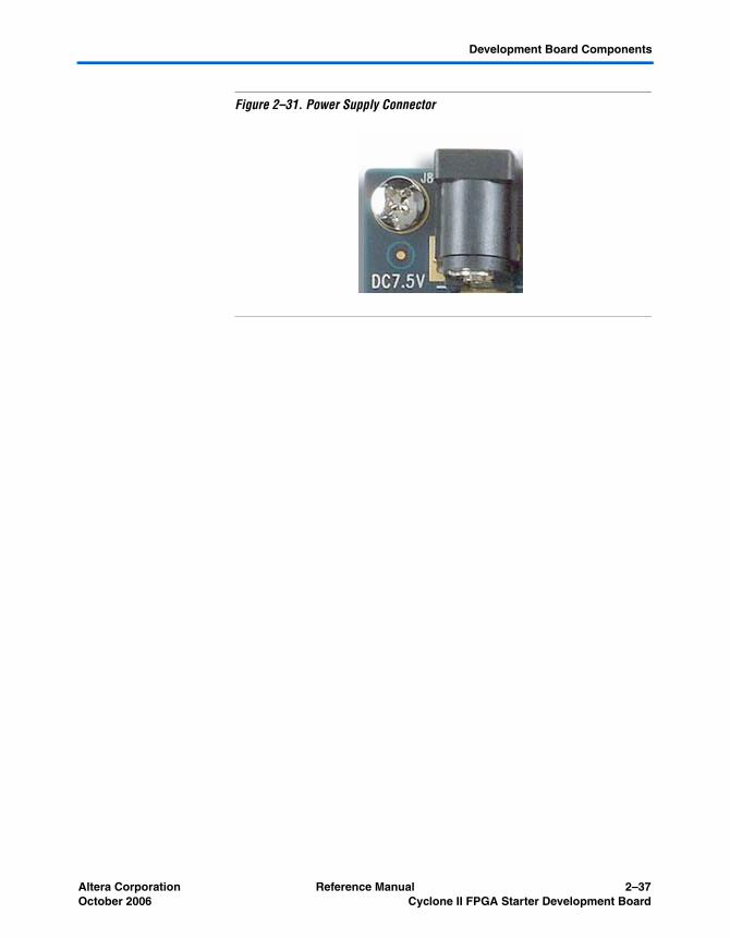
Power Supply Connector
The Cyclone II FPGA Starter board receives its power from either the USB port directly or the included 7.5V power adapter, which plugs into power connector J8 (Figure 2–31).
2–36 Reference Manual Altera CorporationCyclone II FPGA Starter Development Board October 2006
Development Board Components
Figure 2–31. Power Supply Connector
Altera Corporation Reference Manual 2–37October 2006 Cyclone II FPGA Starter Development Board

Development Board Components
2–38 Reference Manual Altera CorporationCyclone II FPGA Starter Development Board October 2006