พายุหมุนเขตร้อน (Tropical Cyclone): กรณีภาคใต้ · พายุหมุนเขตร้อน (Tropical Cyclone): กรณีภาคใต้

101 Innovation DriveSan Jose, CA 95134(408) 544-7000www.altera.com
Cyclone II EP2C35PCI Development Board
Reference Manual
Development Board Version: 1.0.0Document Version: 1.0.0Document Date: May 2005

Copyright © 2005 Altera Corporation. All rights reserved. Altera, The Programmable Solutions Company, the stylized Altera logo, specific device des-ignations, and all other words and logos that are identified as trademarks and/or service marks are, unless noted otherwise, the trademarks andservice marks of Altera Corporation in the U.S. and other countries. All other product or service names are the property of their respective holders. Al-tera products are protected under numerous U.S. and foreign patents and pending applications, maskwork rights, and copyrights. Altera warrantsperformance of its semiconductor products to current specifications in accordance with Altera's standard warranty, but reserves the right to makechanges to any products and services at any time without notice. Altera assumes no responsibility or liability arising out of the ap-plication or use of any information, product, or service described herein except as expressly agreed to in writing by AlteraCorporation. Altera customers are advised to obtain the latest version of device specifications before relying on any published in-formation and before placing orders for products or services.
Development Board Version 1.0.0 Altera CorporationCyclone II EP2C35 PCI Development Board Reference Manual Preliminary May 2005
Part Number MNL-CII021805-1.0
Altera Corporation May 2005
Contents
About This Manual How to Contact Altera .............................................................................................................................. vTypographic Conventions ........................................................................................................................ v
Chapter 1. IntroductionGeneral Description ............................................................................................................................... 1–1
Components ...................................................................................................................................... 1–1Block Diagram .................................................................................................................................. 1–3
Handling the Board ............................................................................................................................... 1–4
Chapter 2. Board Components & InterfacesBoard Overview ..................................................................................................................................... 2–1Component Operation .......................................................................................................................... 2–4
Cyclone II Device .............................................................................................................................. 2–4PCI & PCI-X Bus Support & Compatibility .................................................................................. 2–4Memory .............................................................................................................................................. 2–5Clocks & Clock Distribution ........................................................................................................... 2–6Power ................................................................................................................................................. 2–7LEDs ................................................................................................................................................... 2–9Board DIP Switch Settings ............................................................................................................ 2–11Push-Button Switches .................................................................................................................... 2–13
Interface Operation .............................................................................................................................. 2–14Altera Daughter Card (PROTO1) Interface ................................................................................ 2–1410/100 Ethernet .............................................................................................................................. 2–14RS-232 Serial Interface ................................................................................................................... 2–15AS Interface ..................................................................................................................................... 2–15JTAG ................................................................................................................................................. 2–15SignalTap II Logic Analyzer ......................................................................................................... 2–15Mictor Probe .................................................................................................................................... 2–15
Chapter 3. Using the BoardIntroduction ............................................................................................................................................ 3–1Apply Power to the Board .................................................................................................................... 3–1Configure the Cyclone II Device ......................................................................................................... 3–2
Serial Flash Configuration .............................................................................................................. 3–2JTAG Configuration ......................................................................................................................... 3–3
Program the Serial Flash Memory ....................................................................................................... 3–3Active Serial Programming ............................................................................................................. 3–5In-System Programming via the JTAG & the SFL Solution (User-Programmable EPCS64 Device Only) ................................................................................ 3–7
Configure the Board for Bench-Top Operation ................................................................................. 3–8
iPreliminary

Contents Cyclone II EP2C35 PCI Development Board Reference Manual
Chapter 4. Pin-Outs & Signal SpecificationsIntroduction ............................................................................................................................................ 4–1PCI & PCI-X Bus Interfaces .................................................................................................................. 4–1Memory ................................................................................................................................................... 4–5
DDR2 SDRAM Memory .................................................................................................................. 4–5I/O & Serial I/O .................................................................................................................................... 4–8
10/100 Ethernet ................................................................................................................................ 4–8RS-232 Serial Interface ................................................................................................................... 4–11
Configuration ....................................................................................................................................... 4–11JTAG Header ................................................................................................................................... 4–11AS Interface Header ....................................................................................................................... 4–12EPCS64 Serial Flash Interface ....................................................................................................... 4–12
Control & User Settings ...................................................................................................................... 4–13User LEDs ........................................................................................................................................ 4–13DIP Switch Bank Board & User Settings ..................................................................................... 4–13Push-Button Switches .................................................................................................................... 4–14
Altera Daughter Card & Mictor Probe ............................................................................................. 4–15
ii Altera CorporationPreliminary May 2005
Altera Corporation May 2005
About This Manual
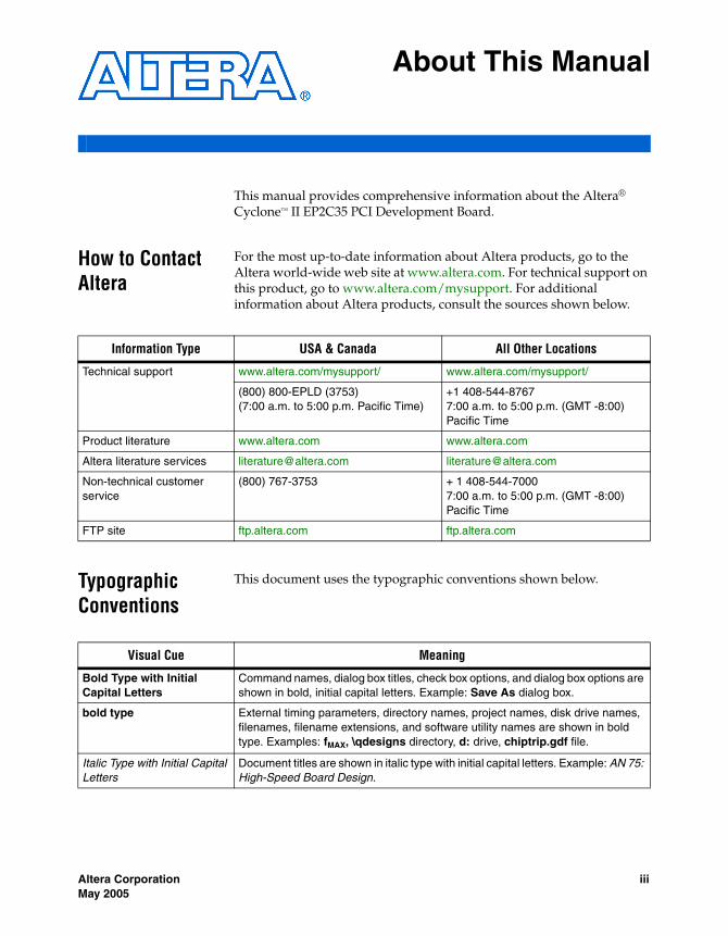
This manual provides comprehensive information about the Altera® Cyclone™ II EP2C35 PCI Development Board.
How to Contact Altera
For the most up-to-date information about Altera products, go to the Altera world-wide web site at www.altera.com. For technical support on this product, go to www.altera.com/mysupport. For additional information about Altera products, consult the sources shown below.
Typographic Conventions
This document uses the typographic conventions shown below.
Information Type USA & Canada All Other Locations
Technical support www.altera.com/mysupport/ www.altera.com/mysupport/
(800) 800-EPLD (3753)(7:00 a.m. to 5:00 p.m. Pacific Time)
+1 408-544-87677:00 a.m. to 5:00 p.m. (GMT -8:00) Pacific Time
Product literature www.altera.com www.altera.com
Altera literature services [email protected] [email protected]
Non-technical customer service
(800) 767-3753 + 1 408-544-70007:00 a.m. to 5:00 p.m. (GMT -8:00) Pacific Time
FTP site ftp.altera.com ftp.altera.com
Visual Cue Meaning
Bold Type with Initial Capital Letters
Command names, dialog box titles, check box options, and dialog box options are shown in bold, initial capital letters. Example: Save As dialog box.
bold type External timing parameters, directory names, project names, disk drive names, filenames, filename extensions, and software utility names are shown in bold type. Examples: fMAX, \qdesigns directory, d: drive, chiptrip.gdf file.
Italic Type with Initial Capital Letters
Document titles are shown in italic type with initial capital letters. Example: AN 75: High-Speed Board Design.
iiiPreliminary
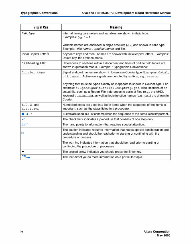
Typographic Conventions Cyclone II EP2C35 PCI Development Board Reference Manual
Italic type Internal timing parameters and variables are shown in italic type. Examples: tPIA, n + 1.
Variable names are enclosed in angle brackets (< >) and shown in italic type. Example: <file name>, <project name>.pof file.
Initial Capital Letters Keyboard keys and menu names are shown with initial capital letters. Examples: Delete key, the Options menu.
“Subheading Title” References to sections within a document and titles of on-line help topics are shown in quotation marks. Example: “Typographic Conventions.”
Courier type Signal and port names are shown in lowercase Courier type. Examples: data1, tdi, input. Active-low signals are denoted by suffix n, e.g., resetn.
Anything that must be typed exactly as it appears is shown in Courier type. For example: c:\qdesigns\tutorial\chiptrip.gdf. Also, sections of an actual file, such as a Report File, references to parts of files (e.g., the AHDL keyword SUBDESIGN), as well as logic function names (e.g., TRI) are shown in Courier.
1., 2., 3., anda., b., c., etc.
Numbered steps are used in a list of items when the sequence of the items is important, such as the steps listed in a procedure.
■ ● • Bullets are used in a list of items when the sequence of the items is not important.
v The checkmark indicates a procedure that consists of one step only.
1 The hand points to information that requires special attention.
cThe caution indicates required information that needs special consideration and understanding and should be read prior to starting or continuing with the procedure or process.
The warning indicates information that should be read prior to starting or continuing the procedure or processes
r The angled arrow indicates you should press the Enter key.
f The feet direct you to more information on a particular topic.
Visual Cue Meaning
iv Altera CorporationPreliminary May 2005
May 2005
1. Introduction
Altera Corporation Core Version a.b.c variable 1–1
General Description
The Cyclone™ II EP2C35 PCI Development Board provides a hardware platform for developing and prototyping high-speed PCI and PCI-X bus interfaces, double data rate 2 (DDR2) SDRAM, and the 10/100 Ethernet interface.
Based on Cyclone II FPGAs and using Altera® MegaCore® functions or Altera Megafunction Partners Program (AMPPSM) megafunctions, the Cyclone II EP2C35 PCI Development Board allows users to quickly solve design problems that typically require time-consuming, custom solutions.
The board supports the EP2C35F672 Cyclone II device, which is optimized for high-bandwidth DSP functions. The board also supports the PCI Local Bus Specification, Revision 3.0 and PCI-X, Revision 2.0 mode 1.
Altera provides a DDR2 SDRAM reference design for use as either a design starting point or an experimental platform. The reference design is designed and tested by Altera engineers and distributed with the PCI Development Kit, Cyclone II Edition (ordering code: PCI-DEVKIT-2C35).
f For more information on the DDR2 SDRAM reference design, refer to AN 390: PCI-to-DDR2 SDRAM Reference Design.
Components
The board provides the following components:
■ Short-form universal PCI (3.3 or 5.0 V) card ● 32 or 64-bit PCI bus operating at 33 or 66 MHz ● 32 or 64-bit PCI-X bus operating at 66 or 100 MHz
■ Memory ● Two 32-MByte DDR2 SDRAM devices ● EPCS64 devices
■ FPGA device configuration ● Switch-selectable on power-up, choose one of two serial
configuration devices (EPCS64 devices). One device contains the pre-loaded factory default design, and the other device is for user-programming. Configuration data is downloaded via the USB-Blaster™ download cable.
■ Flexible clocking options ● Socketed 100-MHz high-speed clock oscillator ● SMA connector clock input
Preliminary

General Description
■ Switches and indicators ● Two user-definable push-button switches ● Five-position, user-definable dual in-line package (DIP) switch
bank ● Eight user-definable LEDs ● Power and configuration status LEDs● Serial port TX/RX activity LEDs● Ethernet LEDs (integrated in RJ45 connector)● Configuration done and status LEDs● Configuration source (local/user) toggle switch
■ Flexible power options ● PCI connector ● External power supply via laptop power supply cable
■ Expansion & Debugging Interfaces● Joint Test Action Group (JTAG) interface connector ● 32-bit Mictor probe connector ● Altera Daughter Card (PROTO1) ● 10/100 Ethernet (RJ-45 connector) ● Serial RS-232 (DB-9 connector)
1–2 Core Version a.b.c variable Altera CorporationCyclone II EP2C35 PCI Development Board Reference Manual May 2005

Introduction
Block Diagram
Figure 1–1 shows the board’s block diagram.
Figure 1–1. PCI Development Board, Cyclone II Edition Block Diagram
EP2C35F672Cyclone II
Device
PCI Bus Switches
64-MByte DDR2 SDRAM Memory
Altera DaughterCard (PROTO1)
Mictor ProbeDebug Connector
10/100 Ethernet
RS-232
JTAG Connector
High-Speed Clock Oscillator
Pushbutton Switches
DIP Switch Settings
User DIP switches
Jumpers
User LEDs
Status LEDs
PowerRegulators
External PowerConnector
Power LEDs
+3.3 V
+1.8 V+1.2 V
PCI, PCI-XConnector
Active Serial Configuration
PCI EdgeConnector
+3.3V
ToggleSwitch
EPCS64 Safe Flash Serial Programmer
EPCS64 User Flash Serial Programmer
SMA Clock Connector
+16 V DC INPUT
Altera Corporation Core Version a.b.c variable 1–3May 2005 Cyclone II EP2C35 PCI Development Board Reference Manual

Handling the Board
Handling the Board
When handling the board, it is important to observe the following precaution:
Static discharge precaution—Without proper anti-static handling the board can be damaged. Therefore, take anti-static precautions while handling the board.
1–4 Core Version a.b.c variable Altera CorporationCyclone II EP2C35 PCI Development Board Reference Manual May 2005

Altera Corporation May 2005
2. Board Components &Interfaces
Board Overview This chapter provides operational and connectivity detail for the board’s major components and interfaces.
f For pin-outs and signal specifications, refer to Chapter 4, Pin-Outs & Signal Specifications.
Figure 2–1 shows a top view of the Cyclone™ II EP2C35 PCI Development Board.
Figure 2–1. Cyclone II EP2C35 PCI Development Board Major Components & Interfaces
User Push-Button Switches
(S1, S5)
UserReset(S3)
ReconfigurePush-Button Switch (S2)
User LEDs(D1 through D8)
Power Switch (SW1)
Altera DaughterCard Interface
(J1, J6, J7)Configuration Status LED
(D10 Botton Red)
Configuration Done LED
(D10 Top Green)
Mictor ProbeConnector (J4)
PCI Level Converters(U13 through U17)
(U20 through U24 on back)
Active Serial Interface
Connector (J11)
User-ProgrammableEPCS64 Device (U7)
Safe (Factory-Programmed)EPCS64 Device (U19 on back)
DDR2 SDRAM (U6, U10)
EPCS64 Device Select Switch (J3)
User (Down) & Safe (Up)
JTAG Connector (J8)
RS-232 (J12)
RS-232 Tx LED(D18) RS-232 Rx LED (D17)
Cyclone II Device (U9)
PCI Connector (J13)
10/100 EthernetMAC/PHY (U3)
User DIP Switch Bank (S4)
SMA Clock (J5)
Ground Test Point (TP1)
Power Indicators (D13 through D15)
VREF Test Point (TP4)
Power Supply Input
10/100 EthernetConnector (RJ1)
Core Version 4.0.0 2–1Preliminary

Board Overview
Table 2–1 lists the board’s major components and interfaces.
Table 2–1. Cyclone II EP2C35 PCI Development Board Components & Interfaces (Part 1 of 2)
Type Component/Interface
Board Reference Description
FPGA Cyclone II device U9 The EP2C35F672 device is installed on the board for the PCI Development Kit, Cyclone II Edition. Note (1)
PCI, PCI-X PCI connector J13 Universal PCI and PCI-X bus interfaces. Refer to Table 2–2 on page 2–4.
PCI level converters U13 through U17, U20 through U24
Level converters for 5.0-V PCI compatibility. Refer to “PCI Level Converters” on page 2–4.
Memory DDR2 SDRAM U6, U10 167 MHz, 32-MByte DDR2 SDRAM
Configuration User and local-serial FLASH memory
U7, U19 Switch-selectable, factory-programmed (safe) EPCS64 or user-programmable EPCS64 for Cyclone II device configuration.
JTAG connector J8 JTAG test and control as well as USB-Blaster configuration interface.
Active serial (AS) connector
J11 AS configuration interface for EPCS64 device programming (may not be installed).
Configuration status LED
D10 (bottom)(red)
Indicates reconfiguration in progress or configuration error.
Configuration done LED
D10 (top) (green)
Indicates Cyclone II configuration is complete.
Clock High-speed clock oscillator
Installed at J9
100-MHz high-speed reference clock.
SMA clock J5 Clock input.
Ethernet clock OSC1 25-MHz Ethernet clock
Control User reset push-button switch
S3 User-defined hardware reset.
Reconfigure push-button switch
S2 Reconfigure Cyclone II device.
PCI ModeDIP switch
S4, position 1
Enables PCI-X extensions. See Table 2–3 on page 2–5.
PCI XSPDDIP switch
S4, position 2
If enabled, selects PCI-X operating speed (i.e., 66 or 133 MHz). See Table 2–5 on page 2–5.
PCI SPD DIP switch
S4, position 3
Selects PCI bus operating speed (66 or 33 MHz). See Table 2–4 on page 2–5.
User settings User push-button switches
S1, S5 User configurable.
User DIP switch bank S4,positions 4-8
User configurable, 5 switches.
2–2 Core Version 4.0.0 Altera CorporationCyclone II EP2C35 PCI Development Board Reference Manual May 2005

Board Components & Interfaces
User indicator User LEDs D1 through D8
User configurable.
Power Power connector J2 External power supply connector.
Power indicators
+5.0-V power OK LED
D15 5.0-V power supply indicator.
+3.3-V power OK LED
D13 3.3-V power supply indicator.
+1.8-V power OK LED
D14 1.8-V power supply indicator.
+1.2-V power OK LED
D16 1.2-V power supply indicator.
Test points VREF TP4 VREF test point near VTT/VREF regulator.
Ground TP1 Ground test point near power connector.
TP2 Ground test point near PWR SWITCH.
TP3 Ground test point near MICTOR.
TP5 Ground test point near oscillator socket.
TP6 Ground test point near DDR2 SDRAM.
TP7 Ground test point near QDRII SRAM.
Expansion interface
Altera® daughter card (PROTO1)
J1, J6, J7 Interface to Altera daughter card (PROTO1).
I/O 10/100 Ethernet U3, RJ1, OSC1
10/100 Ethernet MAC/PHY, RJ-45 connector, 25-MHz oscillator.
Serial I/O RS-232 U12, J12 RS-232 serial interface level shifter, DB9 connector.
RS-232 Tx LED D18 RS-232 transmitter active indicator.
RS-232 Rx LED D17 RS-232 receiver active indicator.
Debug Mictor probe J4 Mictor probe interface for Agilent logic analyzers.
Note to Table 2–1:(1) The Cyclone II EP2C35 PCI Development Board was designed to use either the EP2C35F672, EP2C50F672, or
EP2C70F672 device. However, the board ships with—and was only tested with—the EP2C35F672 device.
Table 2–1. Cyclone II EP2C35 PCI Development Board Components & Interfaces (Part 2 of 2)
Type Component/Interface
Board Reference Description
Altera Corporation Core Version 4.0.0 2–3May 2005 Cyclone II EP2C35 PCI Development Board Reference Manual
Component Operation
Component Operation
This section describes the board’s operation, providing detailed component descriptions.
Cyclone II Device
The Cyclone II device (U9) is connected to all of the board’s components through appropriate on-chip interfaces and board circuitry. The device supports PCI and PCI-X bus interfaces, the DDR2 SDRAM, as well as the 10/100 Ethernet. Users can program the Cyclone II device to implement custom designs.
f For more information on Cyclone II devices, refer to the Cyclone II Device Family Data Sheet section of the Cyclone II Device Handbook.
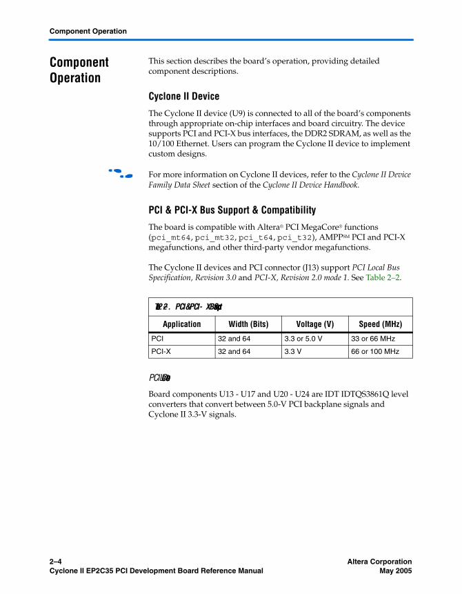
PCI & PCI-X Bus Support & Compatibility
The board is compatible with Altera® PCI MegaCore® functions (pci_mt64, pci_mt32, pci_t64, pci_t32), AMPPSM PCI and PCI-X megafunctions, and other third-party vendor megafunctions.
The Cyclone II devices and PCI connector (J13) support PCI Local Bus Specification, Revision 3.0 and PCI-X, Revision 2.0 mode 1. See Table 2–2.
PCI Level Converters
Board components U13 - U17 and U20 - U24 are IDT IDTQS3861Q level converters that convert between 5.0-V PCI backplane signals and Cyclone II 3.3-V signals.
Table 2–2. PCI & PCI-X Bus Support
Application Width (Bits) Voltage (V) Speed (MHz)
PCI 32 and 64 3.3 or 5.0 V 33 or 66 MHz
PCI-X 32 and 64 3.3 V 66 or 100 MHz
2–4 Core Version 4.0.0 Altera CorporationCyclone II EP2C35 PCI Development Board Reference Manual May 2005

Board Components & Interfaces
PCI Operating Mode, Speed & DIP Switch Settings
Tables 2–3, 2–4, and 2–5 list the board’s PCI operating mode and speed, and the corresponding DIP switch (S4) bank setting.
Memory
The board has the following memory components:
■ Two 32-MByte DDR2 SDRAM devices■ Two EPCS64 serial configuration (flash) devices
DDR2 SDRAM Memory
The board was tested with the Altera 167-MHz, DDR2 SDRAM Controller MegaCore function version 3.2.0. Two 16M × 16 DDR2 SDRAM devices are connected to banks 3 and 4 of the Cyclone II device as a single 16M × 32 memory block.
EPCS64 Serial Configuration (Flash) Devices
The board has two EPCS64Sl16N serial configuration devices (U7 and U19) that upon power-up programs the Cyclone II device. The board contains one EPCS64Sl16N device that is user-programmable, and one preloaded, factory-programmed EPCS64Sl16N device.
Table 2–3. PCI Operating Mode Setting
DIP Switch Position 1 (PCI Mode) PCI Operating Mode
Off PCI-X at the speed shown in Table 2–5.
On PCI at the speed shown in Table 2–4.
Table 2–4. PCI Operating Speed Setting
DIP Switch Position 3 (PCI SPD) PCI Operating Speed (MHz)
Off 66 MHz
On 33 MHz
Table 2–5. PCI-X Operating Speed Setting
DIP Switch Position 2 (PCI XSPD) PCI-X Operating Speed (MHz)
Off 133 or 100 MHz
On 66 MHz
Altera Corporation Core Version 4.0.0 2–5May 2005 Cyclone II EP2C35 PCI Development Board Reference Manual

Component Operation
f For more information on serial configuration devices, refer to the Serial Configuration Devices (EPCS1, EPCS4, EPCS16 & EPCS64) Data Sheet chapter in volume 2 of the Configuration Handbook.
Clocks & Clock Distribution
The board has two clock sources driven directly to the Cyclone II device. Using the PLLs integrated within the Cyclone II device, the designer has significant flexibility to achieve the appropriate clock configuration. Table 2–6 shows the board’s clock sources.
f Refer to the PLLs in Cyclone II Devices chapter in the Cyclone II Device Handbook for more information.
SMA Clock Input Requirements
The SMA clock input, CLK_SMA, can be provided by an external signal source through the J5 connector. Use a 50-Ω signal source and cable with an LVTTL-type signal (square-wave, with a voltage swing from 0.0 to +3.3 V). The maximum CLK_SMA input frequency is 464 MHz; the maximum board frequency with the SMA clock is 500 MHz.
Table 2–6. Cyclone II EP2C35 PCI Development Board Clock Sources
Signal Name Source Destination Primary PLL (1)
LPCIX_CLK PCI connector (J13.B16) through level shifter (U13.13 and U13.11) and resistor (R29)
Cyclone II device (U9.P26) PLL2
OSCA_CLK1 Socketed 100-MHz oscillator (J4.5) through resistor (R61)
Cyclone II device (U9.N1) PLL1
OSCA_CLK6 Socketed 100-MHz oscillator (J4.5) through resistor (R62)
Cyclone II device (U9.P25) PLL2
CLK_SMA SMA clock input connector (J5.1) Cyclone II device (U9.N2) PLL1
CLK_FROM_PROTO1 Altera daughter card (PROTO1) (J7.13)
Cyclone II device (U9.P2) PLL1
DDR2_SYNC_CLK Cyclone II device (U9.B7) Cyclone II device (U9.AF14) PLL4
CLK_25MHZ On-board 25-MHz 10/100 Ethernet oscillator (OSC1.4)
Ethernet MAC/PHY device (U3.127) N/A
Note:(1) A global clock input can directly feed Cyclone II PLLs. Table 2–6 shows the direct connections and does not show
the connection via global clock networks.
2–6 Core Version 4.0.0 Altera CorporationCyclone II EP2C35 PCI Development Board Reference Manual May 2005

Board Components & Interfaces
Cyclone II Output Clocks
Table 2–7 lists the Cyclone II output clocks and their destinations.
Power
This section describes the on-board switching regulators. The board can be powered from one of the following sources:
■ PCI connector J13 supplies +3.3 V and +5.0 V■ Power connector J2 supplies +16 V from external power source
(40 W) that is regulated to 3.3 V
+3.3-V Regulator
The board contains a switching regulator (U2) that takes in the external power source of +9 V to +20 V and regulates down to +3.3 V. All power associated with various required voltage levels are regulated either from the PCI 3.3-V power source or from a 3.3-V power source generated from the power connector (stand-alone operation only). Only one power source is required at a time.
+1.8-V Regulator
A switching regulator (U4) generates +1.8 V for the Cyclone II device I/O and DDR2 SDRAM voltages from +3.3 V.
+1.2-V Regulator
A switching regulator (U1) generates +1.2 V for the Cyclone II internal core voltage from +3.3 V.
Table 2–7. Cyclone II Output Clocks
Signal Name Source Cyclone II Device PLL Destination
DDR2_CK_P0 U9.A22 - DDR2 SDRAM memory (U10.J8)
DDR2_CK_N0 U9.A23 - DDR2 SDRAM memory (U10.K8)
DDR2_CK_P1 U9.A9 - DDR2 SDRAM memory (U6.J8)
DDR2_CK_N1 U9.A8 - DDR2 SDRAM memory (U6.K8)
PLL_TO_PROTO1 U9.V21 PLL4 Altera daughter card (PROTO1)
Altera Corporation Core Version 4.0.0 2–7May 2005 Cyclone II EP2C35 PCI Development Board Reference Manual

Component Operation
External Power Jack
Board header J2 is a power receptacle from a standard laptop power supply. Table 2–8 shows that the external power switch (SW1) enables the external power supply.
1 If both the external power and the PCI power are supplied at the same time, the board draws power from the external power supply for all power rails except the 5.0-V power rail. Therefore, when the PCI 3.3-V circuit transistors detect external power supply voltage, they disable the power from the PCI connector. The external power switch does not control the power from the PCI connector.
Test Points
Table 2–9 shows the board’s power supply test points.
Table 2–8. External Power Supply Enable
External Power Switch (SW1)Position (PWR SWITCH) Description
Off Disable external power supply
On Enable external power supply
Table 2–9. Board’s Power Supply Test Points
Signal Name
Reference Designator Description
VREF TP4 0.9-V VREF for DDR2 SDRAM
Ground TP5 Ground test point near oscillator socket.
TP1 Ground test point near power connector.
TP2 Ground test point near PWR SWITCH.
TP3 Ground test point near MICTOR.
TP6 Ground test point near DDR2 SDRAM.
2–8 Core Version 4.0.0 Altera CorporationCyclone II EP2C35 PCI Development Board Reference Manual May 2005

Board Components & Interfaces
LEDs
This section describes the board’s LED resources.
Power LEDs
There are four power indication LEDs on the board, see Table 2–10.
Status LEDs
Table 2–11 shows the board’s status LEDs.
Table 2–10. Board Power LEDs
Board Reference
Reference Designator Color Description
5.0 V (1) D15 Green 5.0-V power is on.
3.3 V D13 Green 3.3-V power is on.
1.8 V D14 Green 1.8-V power is on.
1.2 V D16 Green 1.2-V power is on.
Note:(1) The power indication LED for +5.0 V requires that the board be plugged into a
PCI slot.
Table 2–11. Board Status LEDs
Board Reference Reference Designator Color Description
CONF_DONE D10.Anode (Top) Green Indicates that the Cyclone II device has been successfully configured.
CONF_STATUSn D10.Cathode(Bottom)
Red Indicates that the Cyclone II device received an error during device configuration.
TX D18 Green Serial cable (RS-232) is transmitting data.
RX D17 Green Serial cable (RS-232) is receiving data.
Altera Corporation Core Version 4.0.0 2–9May 2005 Cyclone II EP2C35 PCI Development Board Reference Manual

Component Operation
Ethernet LEDs
Table 2–12 shows the Ethernet LEDs.
User LEDs
Table 2–13 lists the user LEDs, which are identified as components D1-D8. For information on connecting the user LED signals with the Cyclone II pins, refer to “User LEDs” on page 4–13.
Table 2–12. Ethernet LEDs
Board Reference Reference Designator Color Description
Ethernet RJ45 RJ1 Green Indicates Ethernet link
Ethernet RJ45 RJ1 Yellow Indicates Ethernet link activity
Table 2–13. User LEDs
Number Reference Designator Color Description
0 D8 Green User defined
1 D7 Green User defined
2 D6 Green User defined
3 D5 Green User defined
4 D4 Green User defined
5 D3 Green User defined
6 D2 Green User defined
7 D1 Green User defined
2–10 Core Version 4.0.0 Altera CorporationCyclone II EP2C35 PCI Development Board Reference Manual May 2005

Board Components & Interfaces
Board DIP Switch Settings
Table 2–14 describes the board DIP switch bank (S4) settings.
Table 2–14. Board DIP Switch Settings
Board Reference
Board DIP Switch Settings
Factory Default Setting
Description
PCI XSPD Switch S4 Position 2 On Selects PCI-X bus operating speed. Refer to Table 2–5.
PCI MODE Switch S4 Position 1 On Toggles between PCI and PCI-X operating modes. Refer to Table 2–3.
PCI SPD Switch S4 Position 3 Off Selects PCI bus operating speed. Refer to Table 2–4.
User SW0 Switch S4 Position 4 Off User defined. These DIP switches are directly connected to the Cyclone II device. These switches are momentary-contact, push-button switches that provide stimulus to designs in the Cyclone II device. Each switch is connected to a Cyclone II general purpose I/O pin with a pull-up resistor. When a switch is pressed, the Cyclone II device pin will detect a logic 0; when the switch is not pressed, the Cyclone II device pin will detect a logic 1. The push-button switches are tied high with a pull-up resistor.
User SW1 Switch S4 Position 5 Off
User SW2 Switch S4 Position 6 Off
User SW3 Switch S4 Position 7 Off
User SW4 Switch S4 Position 8 Off
Altera Corporation Core Version 4.0.0 2–11May 2005 Cyclone II EP2C35 PCI Development Board Reference Manual
Component Operation
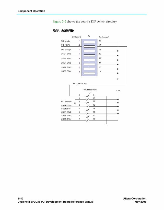
Figure 2–2 shows the board’s DIP switch circuitry.
Figure 2–2. Board User DIP Switch Settings
1
2
3
4
5
6
7
8 9
10
11
12
13
14
15
16
S4 On (closed)Off (open)
PCI Mode
PCI M66EN
USER SW0
USER SW1
USER SW2
USER SW3
USER SW4
3.3V
9
7
6
5
4
3
2
1
8
10
11
12
13
14
15
16
PCI M66EN
USER SW0
USER SW1
USER SW2
USER SW3
USER SW4
PCIX 66SEL133
10K Ω resistors
PCI XSPD
2–12 Core Version 4.0.0 Altera CorporationCyclone II EP2C35 PCI Development Board Reference Manual May 2005

Board Components & Interfaces
Push-Button Switches
Table 2–15 describes the board’s push-button switches.
Figure 2–3 shows the board’s push-button switch circuitry.
Figure 2–3. Board Push-Button Switches
Table 2–15. Push-Button Switches
Board Reference
Reference Designator Description
RECONFIG S2 Causes Cyclone II device to reload configuration
RESET S3 User-defined hardware reset.
PB0 S1 User-defined. These switches are momentary-contact, push-button switches that provide stimulus to designs in the Cyclone II device. Each switch is connected to a Cyclone II general purpose I/O pin with a pull-up resistor. When a switch is pressed, the Cyclone II device pin will detect a logic 0; when the switch is not pressed, the Cyclone II device pin will detect a logic 1. The push-button switches are tied high with a pull-up resistor.
PB1 S5
3.3 V
1
1
1
1
2
2
2
2
S2
S3
S5
S1
RECONFIG
RESETn
USER PB1n
USER PB0n
R35
10K Ω resistors
R40 R33 R34
Altera Corporation Core Version 4.0.0 2–13May 2005 Cyclone II EP2C35 PCI Development Board Reference Manual

Interface Operation
Interface Operation
This section describes the board’s expansion and debugging interface operation.
The board includes the following interfaces:
■ Altera daughter card (PROTO1) ■ 10/100 Ethernet■ RS-232 serial ■ AS interface■ JTAG■ SignalTap® II logic analyzer via the JTAG debug interface■ Mictor probe
Altera Daughter Card (PROTO1) Interface
Board connectors J1, J6, and J7 allow the board to accept optional boards with an Altera daughter card (PROTO1) interface. These connectors can also be used for general purpose debugging, or an expansion interface with 41 pins of LVTTL signals, which are shared with the Mictor probe connector (J4).
Table 2–16 shows the maximum allowed current draw for the Altera daughter card (PROTO1) interface.
f For more information about the following:
■ The Altera daughter card interface and to guarantee a longer life for the card, refer to either the Stratix II or Cyclone II Editions of the Nios Development Board Reference Manuals.
■ Available Altera daughter cards that can be used with the PCI development board, Cyclone II edition, refer to www.altera.com/devkits.
10/100 Ethernet
Board reference U3 is an SMSC LAN91C111 10/100 Ethernet MAC/PHY, and board reference RJ1 is an RJ-45 connector with integrated magnetics and activity LEDs.
Table 2–16. Maximum Allowed Current Draw for Altera Daughter Card
Voltage (V) Maximum Current (A)
3.3 2A
2–14 Core Version 4.0.0 Altera CorporationCyclone II EP2C35 PCI Development Board Reference Manual May 2005

Board Components & Interfaces
RS-232 Serial Interface
Board reference J12 is a DB-9 connector wired as an RS-232 serial DTE device. U12 shifts the RS-232 signals to LVTTL levels for connection to the Cyclone II device.
AS Interface
Board connector J11 provides active serial programming to the EPCS64 device using an Altera USB-Blaster™ cable.
JTAG
Board connector J8 provides access to the board’s JTAG port using a USB-Blaster cable.
SignalTap II Logic Analyzer
The JTAG debug interface can also be used for the Altera SignalTap II logic analyzer.
f For more information on the SignalTap II logic analyzer, refer to the Design Debugging Using the SignalTap II Embedded Logic Analyzer chapter in volume 3 of the Quartus II Handbook.
Mictor Probe
Board connector J4 is a Mictor header that provides probing capability for internal Cyclone II device signals. The Mictor probe is compatible with the Agilent Technologies E5346A Probe Adapter for use with Agilent Technologies Logic Analyzers. The PROTO1 connector signals are shared with the Mictor probe and Altera daughter card interfaces, and the signals on the Mictor header (J4) are shared with the Altera daughter card signals (J1, J6, and J7).
Use the SignalProbe™ incremental routing feature to route internal Cyclone II signals to the J4 connector. You do not need to recompile the Cyclone II device design to use the SignalProbe feature.
f For more information on the SignalProbe feature, refer to the Quick Design Debugging Using Signal Probe chapter in volume 3 of the Quartus II Handbook.
Altera Corporation Core Version 4.0.0 2–15May 2005 Cyclone II EP2C35 PCI Development Board Reference Manual

Interface Operation
2–16 Core Version 4.0.0 Altera CorporationCyclone II EP2C35 PCI Development Board Reference Manual May 2005

Altera Corporation May 2005
3. Using the Board
Introduction This chapter provides step-by-step instructions for using the board. You can configure the board with either the pre-loaded, factory-programmed (safe) design or with a new design. This chapter discusses both.
To configure the board, there are four main steps:
■ Apply power to the board ■ Configure the Cyclone™ II device using either:
● Serial flash configuration● JTAG configuration via either:
• The SRAM object file (.sof)• JTAG indirect configuration (.jic) files and the Cyclone II
device’s Serial FlashLoader (SFL) image■ Program the serial flash memory using either:
● The conventional active serial programming method● The SFL programming scheme for in-system programming via
the JTAG interface■ Configure the board for bench-top operation
Apply Power to the Board
Introduce power in one of the following ways:
■ Install the board in a universal PCI slot ■ Connect an external power supply to the external power connector
(J2)
1 No damage will occur if the external power supply is connected while the board is installed in the PCI slot. When both power sources are applied, the board is designed to operate from the PCI slot’s power supply.
To operate the board with an external power supply, perform the following steps:
1. Insert the connector of a 9 to 20-V laptop power supply into the J2 header.
2. Set the PWR SWITCH (SW1) to the On position. Refer to Table 2–8 on page 2–8.
Core Version 4.0.0 3–1Preliminary

Configure the Cyclone II Device
Configure the Cyclone II Device
The on-board Cyclone II device can be configured in one of two ways:
■ Serial flash configuration■ JTAG configuration
Serial Flash Configuration
Serial flash configuration of the Cyclone II device can be accomplished in two ways:
■ Configuration via user-programmable flash memory■ Configuration via factory-programmed design
Configuration via User-Programmable Flash Memory
The Cyclone II FPGAs use SRAM cells to store configuration data. Because SRAM memory is volatile, configuration data must be downloaded to the Cyclone FPGAs each time power is applied to the board.
The board has a non-volatile configuration scheme that automatically configures the Cyclone II device with either a user-programmable or factory-programmed default design. A switch (J3) is used to select either the user-programmable or the factory-programmed ECPS64 device. In referring to the switch position, the board’s bench-top operation perspective is used. Therefore, when the switch is in the Up position, it is switched away from the bench and in the same direction as the component side of the board; the Down position is in the opposite position.
Upon power-up, the configuration circuit (comprised of the selected EPCS64 device) configures the Cyclone II device. If the switch (J3) is set for user configuration (Down position), the circuit attempts to load the user design. If the load is not successful, the CONF_DONE LED (D10) does not illuminate and the Cyclone II device is not configured. If the load is successful, the CONF_DONE LED illuminates.
Configuration via Factory-Programmed Design
When the factory-programmed design is loaded into the Cyclone II device, the user LEDs blink and the CONF_DONE LED illuminates. To select the factory default design, set the switch (J3) to the Up position.
f For more information on either the user-programmable or factory-programmed design, refer to the PCI Development Kit, Cyclone II Edition Getting Started User Guide.
3–2 Core Version 4.0.0 Altera CorporationCyclone II EP2C35 PCI Development Board Reference Manual May 2005

Using the Board
JTAG Configuration
The Cyclone II device can be configured after power is applied to the board. The JTAG interface permits the Quartus® II software to load the Cyclone II device with a user design through the Altera® USB-Blaster™ download cable. The user design remains in the Cyclone II device until power is removed from the board.
To configure the Cyclone II device using the Quartus II software and the USB-Blaster cable, perform the following steps:
1. Attach the USB-Blaster cable to the J8 header.
2. Open the Quartus II SRAM Object File (.sof) that you want to load into the device. This step launches the Quartus II Programmer.
3. Select USB-Blaster as the hardware. For instructions, refer to Changing the Hardware Setup in Quartus II Help.
4. Set the mode to JTAG.
5. Click Start.
1 If the board is installed into a computer’s PCI slot when it is configured by the USB Blaster cable, the computer system could lock up. If this happens, reset the computer. Do not shut down the computer or the configuration will be lost. Restart the computer to re-enumerate the PCI bus.
Upon successful configuration, the CONF_DONE LED (D10) illuminates.
f For information on how to use the USB-Blaster cable, refer to the following:
■ USB-Blaster Download Cable User Guide■ Quartus II Help
Program the Serial Flash Memory
The serial flash memory can be programmed in one of two ways:
■ Active serial programming■ In-system programming via the JTAG and the SFL solution
1 The in-system programming method via the SFL solution is only for the user-programmable EPCS64 device. The factory-programmed EPCS64 device’s image is not to be replaced.
Altera Corporation Core Version 4.0.0 3–3May 2005 Cyclone II EP2C35 PCI Development Board Reference Manual

Program the Serial Flash Memory
Figure 3–1 illustrates both the conventional (AS programming) method of programming serial configuration devices as well as the in-system programming method using the SFL solution.
Figure 3–1. Conventional Vs In-System Programming Method
The SFL Provides an In-System Programming Solution via the JTAG Interface
JTAG Interface
JTAG Chain
FPGA
SFL Imageto bridge the
JTAG interfaceand ASMI
AS InterfaceASMIJTAG
Conventional Method of Programming Serial Configuration Devices via the AS Interface
FPGASerial
ConfigurationDeviceAS Interface
ByteBlaster II Download Cable, Microprocessor, etc
SerialConfiguration
Device
3–4 Core Version 4.0.0 Altera CorporationCyclone II EP2C35 PCI Development Board Reference Manual May 2005

Using the Board
Table 3–1 lists the advantages and disadvantages of both methods.
Active Serial Programming
This section provides active serial programming steps for both the user-programmable and preloaded, factory-programmed EPCS64 devices.
User-Programmable EPCS64 Device
This section provides the steps to program the user-programmable EPCS64 device’s serial flash memory via the active serial programming method.
To program the user-programmable EPCS64 device’s serial flash memory using the Quartus II software, follow these steps:
1. Write your custom programmer object file (.pof) into flash memory.
f For instructions on either writing a POF to flash memory or creating a POF, refer to Quartus II Help.
2. Choose Programmer (Tools menu). The Chain1.cdf window displays.
3. Scroll to Active Serial Programming in the Mode field.
4. To select the user-programmable EPCS64 device, set the switch (J3) to the Down position.
If the switch (J3) is in the Up position (factory-programmed), the factory-programmed design will be overwritten.
Table 3–1. Advantages & Disadvantages
Method Advantage Disadvantage
Conventional Simple and fast Requires separate programming interface to configure FPGAs and program serial configuration devices.
SFL solution Able to configure the FPGA and program serial configuration devices using the same JTAG interface
Slow because the SFL solution needs to configure the FPGA before programming serial configuration devices.
Altera Corporation Core Version 4.0.0 3–5May 2005 Cyclone II EP2C35 PCI Development Board Reference Manual

Program the Serial Flash Memory
5. Connect the USB-Blaster download cable to the active serial configuration connector, J11.
6. Choose Add File and browse to the POF file.
7. Click Open.
8. Click Start. The user-programmable EPCS64 device is programmed via the active serial header.
To load the program from the user-programmable EPCS64 device to the Cyclone II device, follow these steps:
1. Power-down the board by setting the SW1 switch in the Off position.
2. Perform a power-on reset by setting the SW1 switch in the On position. This will load the user-programmable flash memory data into the Cyclone II device.
Pre-Loaded, Factory-Programmed (Safe) EPCS64 Device
This section provides the steps to load the factory-created reference design into factory-programmed (safe) EPCS64 device’s serial flash memory via the active serial programming method.
To program the pre-loaded, factory-programmed (safe) EPCS64 device’s serial flash memory using the Quartus II software, follow these steps:
1. Choose Programmer (Tools menu). The Chain1.cdf window displays.
2. Scroll to Active Serial Programming in the Mode field.
3. To select the preloaded, factory-programmed EPCS64 device, set the switch (J3) to the Up position.
4. Connect the USB-Blaster download cable to the active serial configuration connector, J11.
5. Choose Add File and browse to the factory-programmed POF file.
6. Click Open.
7. Click Start. The factory-created reference design is loaded into the factory-configuration region of the EPCS64 device via the active serial header.
3–6 Core Version 4.0.0 Altera CorporationCyclone II EP2C35 PCI Development Board Reference Manual May 2005

Using the Board
To load the program from the factory-programmed EPCS64 device to the Cyclone II device, follow these steps:
1. Power-down the board by setting the SW1 switch in the Off position.
2. Perform a power-on reset by setting the SW1 switch in the On position. This will load the factory-created reference design into the Cyclone II device.
In-System Programming via the JTAG & the SFL Solution (User-Programmable EPCS64 Device Only)
Although serial configuration devices do not directly support the JTAG interface, Cyclone II devices have an IP image that can be used as a bridge between the JTAG interface and active serial interface of the serial configuration device. Therefore, JTAG in-system programming is possible for serial configuration devices.
To program the user-programmable EPCS64 device via the SFL solution, follow these steps:
1. Convert the SOF to a JIC file.
2. Use the Quartus II Programmer to program the JIC file into the EPCS64 device. For step-by-step instructions, refer to AN 370: Using the Serial FlashLoader with the Quartus II Software.
The Quartus II software automatically programs the SFL image into the Cyclone II device, erases the EPCS64 device data, and programs the JIC image into the EPCS64 device. This process overwrites the existing image in the Cyclone II device and replaces it with the SFL image.
3. Reconfigure the FPGA with the new configuration data. This can be done by either cycling the power to the board or pressing the Reconfigure switch (S2).
Altera Corporation Core Version 4.0.0 3–7May 2005 Cyclone II EP2C35 PCI Development Board Reference Manual

Configure the Board for Bench-Top Operation
Configure the Board for Bench-Top Operation
The development board is initially configured for installation in a conventional PCI slot. Five standoffs and five screws are included for bench-top operation.
To configure the board for bench-top operation, follow these steps:
1. Position the board face up with the PCI bracket on the left.
2. Insert a screw in the hole next to PWR SWITCH (SW1) and fasten a standoff to the screw.
3. Insert a screw in the hole next to RS-232 LEDs (D17 and D18) and fasten a standoff to the screw.
4. Insert a screw in between J6 and J7 and fasten a standoff to the screw.
5. Insert a screw in the hole next to external power jack (J2) and fasten a standoff to the screw.
6. Insert a screw in the lower right corner next to J11 and fasten a standoff to the screw.
To configure the board, perform the following steps:
1. Create a POF for your design.
2. Write the POF into flash memory.
3. Select the user-programmable EPCS64 device by setting the switch (J3) to the Down position.
4. Force the device to reconfigure by pressing the RECONFIG push-button (S2).
3–8 Core Version 4.0.0 Altera CorporationCyclone II EP2C35 PCI Development Board Reference Manual May 2005
Altera Corporation May 2005
4. Pin-Outs & SignalSpecifications
Introduction This chapter provides the following board pin-out and signal specifications:
■ PCI & PCI-X bus interfaces■ Memory■ I/O■ Configuration■ Control & user settings■ Altera® daughter card
PCI & PCI-X Bus Interfaces
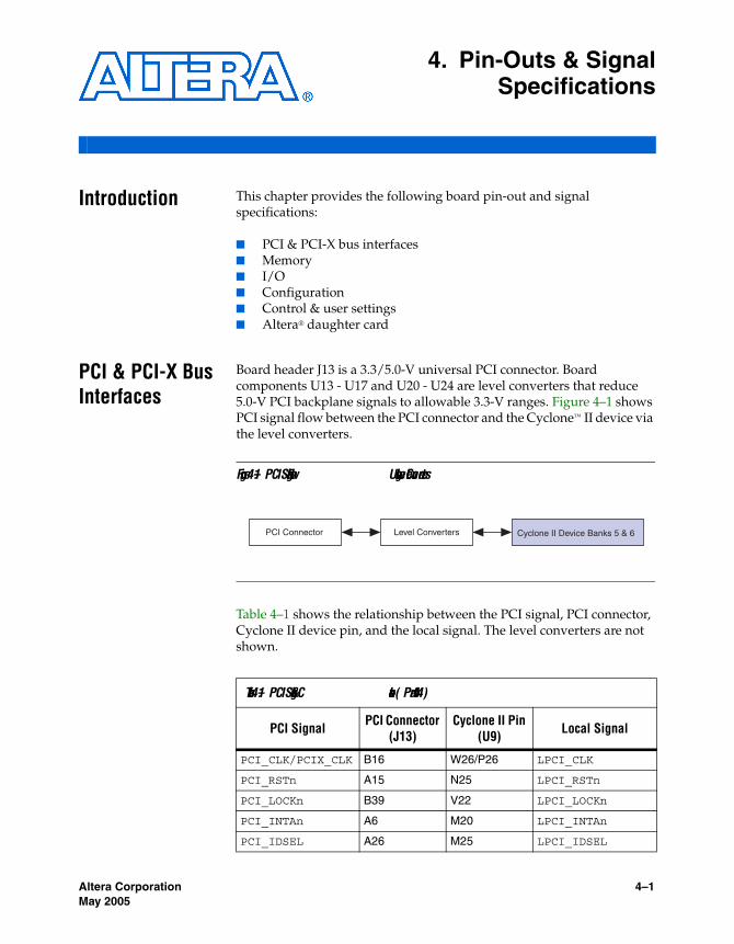
Board header J13 is a 3.3/5.0-V universal PCI connector. Board components U13 - U17 and U20 - U24 are level converters that reduce 5.0-V PCI backplane signals to allowable 3.3-V ranges. Figure 4–1 shows PCI signal flow between the PCI connector and the Cyclone™ II device via the level converters.
Figure 4–1. PCI Signal Flow Using Level Converters
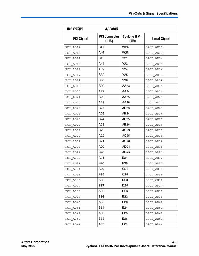
Table 4–1 shows the relationship between the PCI signal, PCI connector, Cyclone II device pin, and the local signal. The level converters are not shown.
Table 4–1. PCI Signals & Connections (Part 1 of 4)
PCI Signal PCI Connector (J13)
Cyclone II Pin (U9) Local Signal
PCI_CLK/PCIX_CLK B16 W26/P26 LPCI_CLK
PCI_RSTn A15 N25 LPCI_RSTn
PCI_LOCKn B39 V22 LPCI_LOCKn
PCI_INTAn A6 M20 LPCI_INTAn
PCI_IDSEL A26 M25 LPCI_IDSEL
PCI Connector Level Converters Cyclone II Device Banks 5 & 6
Core Version 4.0.0 4–1Preliminary

PCI & PCI-X Bus Interfaces
PCI_REQn B18 N20 LPCI_REQn
PCI_REQ64n A60 V26 LPCI_REQ64n
PCI_GNTn A17 M24 LPCI_GNTn
PCI_ACK64n B60 V25 LPCI_ACK64n
PCI_FRAMEn A34 N24 LPCI_FRAMEn
PCI_DEVSELn B37 R25 LPCI_DEVSELn
PCI_IRDYn B35 P23 LPCI_IRDYn
PCI_TRDYn A36 N23 LPCI_TRDYn
PCI_STOPn A38 P24 LPCI_STOPn
PCI_PAR A43 T20 LPCI_PAR
PCI_PAR64 A67 U26 LPCI_PAR64
PCI_PERRn B40 U24 LPCI_PERRn
PCI_SERRn B42 U23 LPCI_SERRn
PCI_CBEn0 A52 R20 LPCI_CBEn0
PCI_CBEn1 B44 T22 LPCI_CBEn1
PCI_CBEn2 B33 T24 LPCI_CBEn2
PCI_CBEn3 B26 T25 LPCI_CBEn3
PCI_CBEn4 B66 U20 LPCI_CBEn4
PCI_CBEn5 A65 U21 LPCI_CBEn5
PCI_CBEn6 B65 V24 LPCI_CBEn6
PCI_CBEn7 A64 V23 LPCI_CBEn7
PCI_AD0 A58 L20 LPCI_AD0
PCI_AD1 B58 L21 LPCI_AD1
PCI_AD2 A57 L24 LPCI_AD2
PCI_AD3 B56 L25 LPCI_AD3
PCI_AD4 A55 M19 LPCI_AD4
PCI_AD5 B55 M22 LPCI_AD5
PCI_AD6 A54 M23 LPCI_AD6
PCI_AD7 B53 R24 LPCI_AD7
PCI_AD8 B52 U22 LPCI_AD8
PCI_AD9 A49 U25 LPCI_AD9
PCI_AD10 B48 W21 LPCI_AD10
PCI_AD11 A47 W23 LPCI_AD11
Table 4–1. PCI Signals & Connections (Part 2 of 4)
PCI Signal PCI Connector (J13)
Cyclone II Pin (U9) Local Signal
4–2 Core Version 4.0.0 Altera CorporationCyclone II EP2C35 PCI Development Board Reference Manual May 2005
Pin-Outs & Signal Specifications
PCI_AD12 B47 W24 LPCI_AD12
PCI_AD13 A46 W25 LPCI_AD13
PCI_AD14 B45 Y21 LPCI_AD14
PCI_AD15 A44 Y23 LPCI_AD15
PCI_AD16 A32 Y24 LPCI_AD16
PCI_AD17 B32 Y25 LPCI_AD17
PCI_AD18 B30 Y26 LPCI_AD18
PCI_AD19 B30 AA23 LPCI_AD19
PCI_AD20 A29 AA24 LPCI_AD20
PCI_AD21 B29 AA25 LPCI_AD21
PCI_AD22 A28 AA26 LPCI_AD22
PCI_AD23 B27 AB23 LPCI_AD23
PCI_AD24 A25 AB24 LPCI_AD24
PCI_AD25 B24 AB25 LPCI_AD25
PCI_AD26 A23 AB26 LPCI_AD26
PCI_AD27 B23 AC23 LPCI_AD27
PCI_AD28 A22 AC25 LPCI_AD28
PCI_AD29 B21 AC26 LPCI_AD29
PCI_AD30 A20 AD24 LPCI_AD30
PCI_AD31 B20 AD25 LPCI_AD31
PCI_AD32 A91 B24 LPCI_AD32
PCI_AD33 B90 B25 LPCI_AD33
PCI_AD34 A89 C24 LPCI_AD34
PCI_AD35 B89 C25 LPCI_AD35
PCI_AD36 A88 D23 LPCI_AD36
PCI_AD37 B87 D25 LPCI_AD37
PCI_AD38 A86 D26 LPCI_AD38
PCI_AD39 B86 E22 LPCI_AD39
PCI_AD40 A85 E23 LPCI_AD40
PCI_AD41 B84 E24 LPCI_AD41
PCI_AD42 A83 E25 LPCI_AD42
PCI_AD43 B83 E26 LPCI_AD43
PCI_AD44 A82 F23 LPCI_AD44
Table 4–1. PCI Signals & Connections (Part 3 of 4)
PCI Signal PCI Connector (J13)
Cyclone II Pin (U9) Local Signal
Altera Corporation Core Version 4.0.0 4–3May 2005 Cyclone II EP2C35 PCI Development Board Reference Manual

PCI & PCI-X Bus Interfaces
Table 4–2 shows the PCI system configuration signals.
PCI_AD45 B81 F25 LPCI_AD45
PCI_AD46 A80 F26 LPCI_AD46
PCI_AD47 B80 G21 LPCI_AD47
PCI_AD48 A79 G22 LPCI_AD48
PCI_AD49 B78 G23 LPCI_AD49
PCI_AD50 A77 G26 LPCI_AD50
PCI_AD51 B77 H23 LPCI_AD51
PCI_AD52 A76 H25 LPCI_AD52
PCI_AD53 B75 H26 LPCI_AD53
PCI_AD54 A74 J20 LPCI_AD54
PCI_AD55 B74 J21 LPCI_AD55
PCI_AD56 A73 J23 LPCI_AD56
PCI_AD57 B72 J24 LPCI_AD57
PCI_AD58 A71 J25 LPCI_AD58
PCI_AD59 B71 J26 LPCI_AD59
PCI_AD60 A70 K22 LPCI_AD60
PCI_AD61 B69 K23 LPCI_AD61
PCI_AD62 A68 K25 LPCI_AD62
PCI_AD63 B68 K26 LPCI_AD63
Table 4–1. PCI Signals & Connections (Part 4 of 4)
PCI Signal PCI Connector (J13)
Cyclone II Pin (U9) Local Signal
Table 4–2. PCI System Configuration Signals
Board ReferenceBoard Settings DIP
Switch Bank Positions (S4)
PCI Signal PCI Connector (J13) Attribute
PCI SPD Switch S4, position 3 PCI_M66EN B49 Ground
PCI Mode Switch S4, position 1 PCI_XCAP B38 Ground
PCI XSPD Switch S4, position 2 10-K Ω resistor to ground
4–4 Core Version 4.0.0 Altera CorporationCyclone II EP2C35 PCI Development Board Reference Manual May 2005

Pin-Outs & Signal Specifications
Memory This section describes the DDR2 memory pin-outs and signal specifications.
DDR2 SDRAM Memory
The DDR2 SDRAM memory devices installed at U6 and U10 use SSTL-1.8 Class II signaling and termination. A reference voltage of 0.9 V is supplied to banks 3 and 4 for SSTL-1.8 receiver biasing. On-board resistors provide terminations in both ‘fly-by’ and non ‘fly-by’ orientations. Figure 4–2 shows the DDR2 SDRAM memory termination connections for the data, data strobe, and data mask pins. The on-board DDR2 SDRAM memory devices share their pins on the Cyclone II device for address and control nets, whereas the data nets are independent.
Figure 4–2. DDR2 SDRAM Memory Termination Connections
Table 4–3 shows the DDR2 SDRAM memory and termination signal connections.
Cyclone II Banks 3 & 4
256-Mb DDR2 SDRAM Device 1
Non Fly-By Termination Resistors
256-Mb DDR2 SDRAM Device 2
Fly-By Termination Resistors
Fly-By Termination Resistors
Table 4–3. DDR2 SDRAM Memory & Terminator Signal Connections (Part 1 of 3)
DDR2 SDRAM Signal
DDR2 SDRAM Device 1 (U6)
DDR2 SDRAM Device 2 (U10)
Non Fly-By Terminator
Fly-By Terminator
Cyclone II Pin (U9)
DDR2_CLKEN0 K2 K2 N/A RN11.2 D21
DDR2_CSn0 L8 L8 N/A RN11.6 C23
DDR2_RASn K7 K7 N/A RN9.1 D7
DDR2_CASn L7 L7 N/A RN13.4 F9
DDR2_WEn K3 K3 N/A RN9.2 C7
DDR2_ODT K9 K9 N/A RN13.3 G9
DDR2_A0 M8 M8 N/A RN13.2 A19
Altera Corporation Core Version 4.0.0 4–5May 2005 Cyclone II EP2C35 PCI Development Board Reference Manual

Memory
DDR2_A1 M3 M3 N/A RN13.6 A20
DDR2_A2 M7 M7 N/A RN11.4 A21
DDR2_A3 N2 N2 N/A RN13.8 B19
DDR2_A4 N8 N8 N/A RN11.1 B21
DDR2_A5 N3 N3 N/A RN11.7 B22
DDR2_A6 N7 N7 N/A RN13.1 C19
DDR2_A7 P2 P2 N/A RN13.7 D18
DDR2_A8 P8 P8 N/A R25 D19
DDR2_A9 P3 P3 N/A RN13.5 D20
DDR2_A10 M2 M2 N/A RN9.3 A4
DDR2_A11 P7 P7 N/A RN9.5 A5
DDR2_A12 R2 R2 N/A RN9.7 B4
DDR2_A13 R8 R8 N/A RN9.6 B5
DDR2_A14 R3 R3 N/A RN9.8 B6
DDR2_A15 R7 R7 N/A RN9.4 C4
DDR2_BA0 L2 L2 N/A RN11.8 C22
DDR2_BA1 L3 L3 N/A RN11.5 C21
DDR2_BA2 L1 L1 N/A R21 C11
DDR2_DQS0 - F7 RN14.3 RN17.1 C17
DDR2_DQS1 - B7 RN10.8 RN16.5 B14
DDR2_DQS2 F7 - RN7.8 RN3.4 B8
DDR2_DQS3 B7 - RN6.7 RN2.4 C12
DDR2_DM0 - F3 RN14.5 RN17.3 C16
DDR2_DM1 - B3 RN12.6 RN16.4 G12
DDR2_DM2 F3 - RN7.3 RN3.7 D6
DDR2_DM3 B3 - RN6.2 RN2.3 B9
DDR2_DQ0 - G8 RN14.4 RN15.8 A18
DDR2_DQ1 - G2 RN14.8 RN17.6 G16
DDR2_DQ2 - H7 RN14.6 RN15.7 F16
DDR2_DQ3 - H3 RN12.8 RN17.2 F15
DDR2_DQ4 - H1 RN14.7 RN17.5 G15
DDR2_DQ5 - H9 RN14.1 RN15.5 B17
DDR2_DQ6 - F1 RN14.2 RN17.4 A17
Table 4–3. DDR2 SDRAM Memory & Terminator Signal Connections (Part 2 of 3)
DDR2 SDRAM Signal
DDR2 SDRAM Device 1 (U6)
DDR2 SDRAM Device 2 (U10)
Non Fly-By Terminator
Fly-By Terminator
Cyclone II Pin (U9)
4–6 Core Version 4.0.0 Altera CorporationCyclone II EP2C35 PCI Development Board Reference Manual May 2005

Pin-Outs & Signal Specifications
DDR2_DQ7 - F9 RN12.7 RN15.6 E15
DDR2_DQ8 - C8 RN12.3 RN16.6 B16
DDR2_DQ9 - C2 RN12.2 RN16.1 B15
DDR2_DQ10 - D7 RN12.4 RN16.3 C15
DDR2_DQ11 - D3 RN10.6 RN16.2 G13
DDR2_DQ12 - D1 RN12.1 RN17.7 G14
DDR2_DQ13 - D9 RN10.7 RN16.7 F14
DDR2_DQ14 - B1 RN12.5 RN17.8 D14
DDR2_DQ15 - B9 RN10.5 RN16.8 B11
DDR2_DQ16 G8 - RN10.4 RN3.6 F11
DDR2_DQ17 G2 - RN10.2 RN4.3 C9
DDR2_DQ18 H7 - RN10.3 RN3.8 D9
DDR2_DQ19 H3 - RN7.4 RN4.1 G10
DDR2_DQ20 H1 - RN7.5 RN4.4 F10
DDR2_DQ21 H9 - RN10.1 RN3.5 C8
DDR2_DQ22 F1 - RN7.6 RN4.2 D8
DDR2_DQ23 F9 - RN7.7 RN3.3 A7
DDR2_DQ24 C8 - RN7.2 RN2.7 F12
DDR2_DQ25 C2 - RN6.8 RN2.5 D12
DDR2_DQ26 D7 - RN7.1 RN3.1 E12
DDR2_DQ27 D3 - RN6.1 RN3.2 G11
DDR2_DQ28 D1 - RN6.5 RN2.2 A10
DDR2_DQ29 D9 - RN6.4 RN2.8 B10
DDR2_DQ30 B1 - RN6.6 RN2.1 D10
DDR2_DQ31 B9 - RN6.3 RN2.6 C10
Table 4–3. DDR2 SDRAM Memory & Terminator Signal Connections (Part 3 of 3)
DDR2 SDRAM Signal
DDR2 SDRAM Device 1 (U6)
DDR2 SDRAM Device 2 (U10)
Non Fly-By Terminator
Fly-By Terminator
Cyclone II Pin (U9)
Altera Corporation Core Version 4.0.0 4–7May 2005 Cyclone II EP2C35 PCI Development Board Reference Manual

I/O & Serial I/O
Table 4–4 shows the DDR2 SDRAM memory clock signal connections.
I/O & Serial I/O This section describes signal specifications for the following interfaces:
■ 10/100 Ethernet■ RS-232 serial interface
10/100 Ethernet
Table 4–5 shows the 10/100 Ethernet interface signal connections.
Table 4–4. DDR2 SDRAM Memory Clock Signal Connections
Clock SignalDDR2 SDRAM
Memory Device 1 (U6)
DDR2 SDRAM Memory
Device 1 (U10)
Cyclone II Pin (U9)
DDR2_CK_N0 – K8 A23
DDR2_CK_P0 – J8 A22
DDR2_CK_N1 K8 – A8
DDR2_CK_P1 J8 – A9
DDR2_SYNC_CLK_IN – – AF14
DDR2_SYNC_CLK_OUT – – B7
Table 4–5. 10/100 Ethernet Interface Signal Connections (Part 1 of 3)
Ethernet Signal Connector Pin (RJ1) MAC/PHY Pin (U3) Cyclone II
Pin (U9)
LAN_TXDp RJ1.1 U3.14 –
LAN_TXDn RJ1.3 U3.15 –
LAN_RXDp RJ1.4 U3.17 (through resistor R49) –
LAN_RXDn RJ1.6 U3.18 (through resistor R53) –
LAN_LEDA_n RJ1.10 U3.22 –
LAN_LEDB_n RJ1.12 U3.23 –
LAN_BEn0 – U3.94 U5
LAN_BEn1 – U3.95 U6
LAN_BEn2 – U3.96 U7
LAN_BEn3 – U3.97 V1
LAN_AEN – U3.41 V4
LAN_A1 – U3.78 V7
4–8 Core Version 4.0.0 Altera CorporationCyclone II EP2C35 PCI Development Board Reference Manual May 2005

Pin-Outs & Signal Specifications
LAN_A2 – U3.79 W1
LAN_A3 – U3.80 W3
LAN_A4 – U3.81 W6
LAN_A5 – U3.82 Y1
LAN_A6 – U3.83 Y3
LAN_A7 – U3.84 Y4
LAN_A8 – U3.85 Y5
LAN_A9 – U3.86 P3
LAN_A10 – U3.87 P4
LAN_A11 – U3.88 R3
LAN_A12 – U3.89 B2
LAN_A13 – U3.90 J7
LAN_A14 – U3.91 J8
LAN_A15 – U3.92 L6
LAN_D0 – U3.107 AA1
LAN_D1 – U3.106 AA2
LAN_D2 – U3.105 AA3
LAN_D3 – U3.104 AA4
LAN_D4 – U3.102 AA5
LAN_D5 – U3.101 AB1
LAN_D6 – U3.100 AB2
LAN_D7 – U3.99 AB3
LAN_D8 – U3.76 AB4
LAN_D9 – U3.75 AC1
LAN_D10 – U3.74 AC2
LAN_D11 – U3.73 AC3
LAN_D12 – U3.71 AD2
LAN_D13 – U3.70 AD3
LAN_D14 – U3.69 AE2
LAN_D15 – U3.68 AE3
LAN_D16 – U3.66 P6
LAN_D17 – U3.65 P7
LAN_D18 – U3.64 R2
Table 4–5. 10/100 Ethernet Interface Signal Connections (Part 2 of 3)
Ethernet Signal Connector Pin (RJ1) MAC/PHY Pin (U3) Cyclone II
Pin (U9)
Altera Corporation Core Version 4.0.0 4–9May 2005 Cyclone II EP2C35 PCI Development Board Reference Manual

I/O & Serial I/O
LAN_D19 – U3.63 R4
LAN_D20 – U3.61 R5
LAN_D21 – U3.60 R6
LAN_D22 – U3.59 R7
LAN_D23 – U3.58 T2
LAN_D24 – U3.56 T3
LAN_D25 – U3.55 T4
LAN_D26 – U3.54 T6
LAN_D27 – U3.53 T7
LAN_D28 – U3.51 U1
LAN_D29 – U3.50 U2
LAN_D30 – U3.49 U3
LAN_D31 – U3.48 U4
LAN_RESET – U3.30 V2
LAN_ADSn – U3.37 W4
LAN_CLK – U3.42 AA7
LAN_IOCHRDY – U3.38 Y22
LAN_RDYRTNn – U3.46 T23
LAN_SRDYn – U3.43 N26
LAN_INRTQ0 – U3.29 V3
LAN_LDEVn – U3.45 P1
LAN_IORn – U3.31 V5
LAN_IOWn – U3.32 V6
LAN_DATACSn – U3.34 H24
LAN_CYCLEn – U3.35 J5
LAN_W_Rn – U3.36 F6
LAN_VLBUSn – U3.40 E5
LAN_LOOPBACK – U3.21 W2
Table 4–5. 10/100 Ethernet Interface Signal Connections (Part 3 of 3)
Ethernet Signal Connector Pin (RJ1) MAC/PHY Pin (U3) Cyclone II
Pin (U9)
4–10 Core Version 4.0.0 Altera CorporationCyclone II EP2C35 PCI Development Board Reference Manual May 2005
Pin-Outs & Signal Specifications
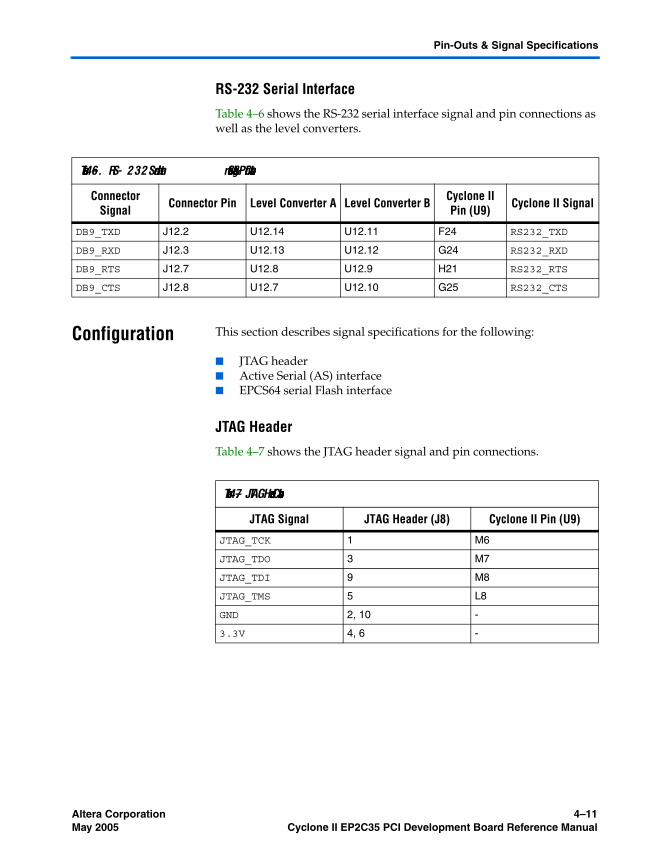
RS-232 Serial Interface
Table 4–6 shows the RS-232 serial interface signal and pin connections as well as the level converters.
Configuration This section describes signal specifications for the following:
■ JTAG header■ Active Serial (AS) interface■ EPCS64 serial Flash interface
JTAG Header
Table 4–7 shows the JTAG header signal and pin connections.
Table 4–6. RS-232 Serial Interface Signal & Pin Connections
Connector Signal Connector Pin Level Converter A Level Converter B Cyclone II
Pin (U9) Cyclone II Signal
DB9_TXD J12.2 U12.14 U12.11 F24 RS232_TXD
DB9_RXD J12.3 U12.13 U12.12 G24 RS232_RXD
DB9_RTS J12.7 U12.8 U12.9 H21 RS232_RTS
DB9_CTS J12.8 U12.7 U12.10 G25 RS232_CTS
Table 4–7. JTAG Header Connections
JTAG Signal JTAG Header (J8) Cyclone II Pin (U9)
JTAG_TCK 1 M6
JTAG_TDO 3 M7
JTAG_TDI 9 M8
JTAG_TMS 5 L8
GND 2, 10 -
3.3V 4, 6 -
Altera Corporation Core Version 4.0.0 4–11May 2005 Cyclone II EP2C35 PCI Development Board Reference Manual

Configuration
AS Interface Header
Table 4–8 shows the AS interface header connections.
EPCS64 Serial Flash Interface
Table 4–9 shows the EPCS64 serial flash interface signal and pin connections for both the user-programmable and preloaded, factory-programmed serial flash devices.
Table 4–8. AS Interface Header Connections
AS Signal AS Connector (J8)
CONF_DCLK 1
CONF_DONE 3
CONF_CONFIGn 5
CONF_DATA0 7
CONF_ASD0 9
CONF_CEn 6
CONF_CS0n 8
GND 2, 10
3.3V 4
Table 4–9. EPCS64 Serial Flash Interface Connections
EPCS64 Serial Flash Signal
User-Programmable EPCS64 Device
(U7)
Factory-Programmed
EPCS64 Device (U19)
Cyclone II Pin (U9)
CONF_DCLK 16 16 N6
CONF_DATA0 8 8 N3
CONF_ASD0 15 15 E3
CONF_CS0n – – D3
CONF_USER_CS0n 7 – G18
CONF_SAFE_CS0n – 7 G17
4–12 Core Version 4.0.0 Altera CorporationCyclone II EP2C35 PCI Development Board Reference Manual May 2005
Pin-Outs & Signal Specifications
Control & User Settings
This section describes pin-outs and signal specifications for:
■ User LEDs■ DIP switch bank board & user settings■ Push-button switches
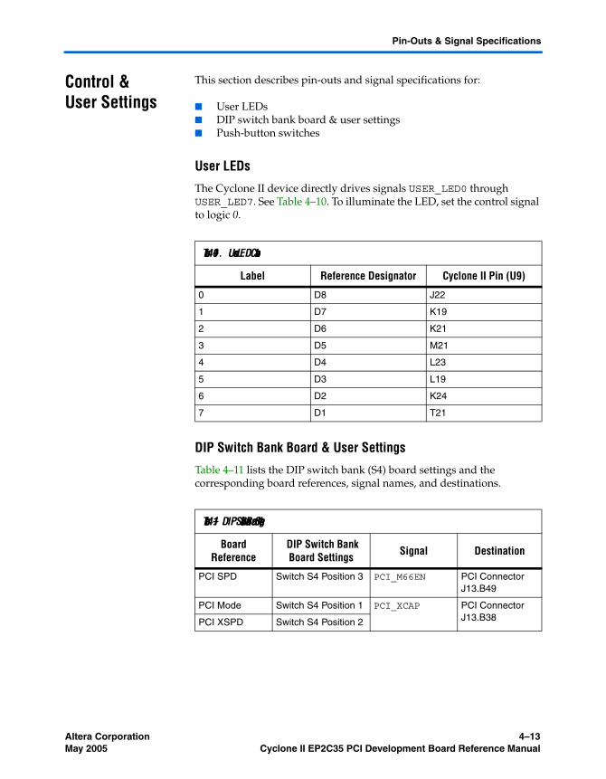
User LEDs
The Cyclone II device directly drives signals USER_LED0 through USER_LED7. See Table 4–10. To illuminate the LED, set the control signal to logic 0.
DIP Switch Bank Board & User Settings
Table 4–11 lists the DIP switch bank (S4) board settings and the corresponding board references, signal names, and destinations.
Table 4–10. User LED Connections
Label Reference Designator Cyclone II Pin (U9)
0 D8 J22
1 D7 K19
2 D6 K21
3 D5 M21
4 D4 L23
5 D3 L19
6 D2 K24
7 D1 T21
Table 4–11. DIP Switch Bank Board Settings
Board Reference
DIP Switch Bank Board Settings Signal Destination
PCI SPD Switch S4 Position 3 PCI_M66EN PCI Connector J13.B49
PCI Mode Switch S4 Position 1 PCI_XCAP PCI Connector J13.B38 PCI XSPD Switch S4 Position 2
Altera Corporation Core Version 4.0.0 4–13May 2005 Cyclone II EP2C35 PCI Development Board Reference Manual

Control & User Settings
Table 4–12 shows the user DIP switch bank (S4) signal names, board references, and pin connections.
Push-Button Switches
Table 4–13 shows the push-button switch signal names and pin connections.
Table 4–12. User DIP Switch Bank Settings
Board Reference User DIP Switch Signal Cyclone II Pin (U9)
0 Switch S4 Position 4 USER_SW0 AA12
1 Switch S4 Position 5 USER_SW1 AB8
2 Switch S4 Position 6 USER_SW2 AC6
3 Switch S4 Position 7 USER_SW3 AD12
4 Switch S4 Position 8 USER_SW4 AD8
Table 4–13. Push-Button Switch Signal Names & Pin Connections
Board Reference Pin Signal Cyclone II Pin (U9)
RESET S3.2 SYS_RESETn C5
RECONFIG S2.2 CONFIG_PBn R23 (through diode U18)
PB0 S1.2 USER_PB0n B12
PB1 S5.2 USER_PB1n D13
4–14 Core Version 4.0.0 Altera CorporationCyclone II EP2C35 PCI Development Board Reference Manual May 2005
Pin-Outs & Signal Specifications
Altera Daughter Card & Mictor Probe
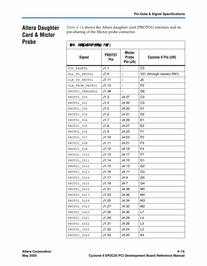
Table 4–14 shows the Altera daughter card (PROTO1) interface and its pin-sharing of the Mictor probe connector.
Table 4–14. Altera Daughter Card & Mictor Probe Pin Sharing (Part 1 of 2)
Signal PROTO1 Pin
Mictor Probe
Pin (J4)Cyclone II Pin (U9)
SYS_RESETn J1.1 – C5
PLL_TO_PROTO1 J7.9 – V21 (through resistor R87)
CLK_TO_PROTO1 J7.11 – J6
CLK_FROM_PROTO1 J7.13 – P2
PROTO1_CARDSELn J1.38 – G6
PROTO1_IO0 J1.3 J4.37 C2
PROTO1_IO1 J1.4 J4.35 C3
PROTO1_IO2 J1.5 J4.33 D1
PROTO1_IO3 J1.6 J4.31 D2
PROTO1_IO4 J1.7 J4.29 E1
PROTO1_IO5 J1.8 J4.27 E2
PROTO1_IO6 J1.9 J4.25 F1
PROTO1_IO7 J1.10 J4.23 F2
PROTO1_IO8 J1.11 J4.21 F3
PROTO1_IO9 J1.12 J4.19 F4
PROTO1_IO10 J1.13 J4.17 F7
PROTO1_IO11 J1.14 J4.15 G1
PROTO1_IO12 J1.15 J4.13 G2
PROTO1_IO13 J1.16 J4.11 G3
PROTO1_IO14 J1.17 J4.9 G5
PROTO1_IO15 J1.18 J4.7 G4
PROTO1_IO16 J1.21 J4.38 M5
PROTO1_IO17 J1.23 J4.36 M4
PROTO1_IO18 J1.25 J4.34 M3
PROTO1_IO19 J1.27 J4.32 M2
PROTO1_IO20 J1.28 J4.30 L7
PROTO1_IO21 J1.29 J4.28 L4
PROTO1_IO22 J1.31 J4.26 L3
PROTO1_IO23 J1.32 J4.24 L2
PROTO1_IO24 J1.33 J4.22 K4
Altera Corporation Core Version 4.0.0 4–15May 2005 Cyclone II EP2C35 PCI Development Board Reference Manual

Altera Daughter Card & Mictor Probe
PROTO1_IO25 J1.35 J4.20 K3
PROTO1_IO26 J1.36 J4.18 K2
PROTO1_IO27 J1.37 J4.16 K1
PROTO1_IO28 J1.39 J4.14 J4
PROTO1_IO29 J6.4 J4.12 J3
PROTO1_IO30 J6.5 J4.10 J2
PROTO1_IO31 J6.6 J4.8 J1
PROTO1_IO32 J6.7 J4.5 H4
PROTO1_IO33 J6.8 J4.6 H3
PROTO1_IO34 J6.9 – H2
PROTO1_IO35 J6.10 – H1
PROTO1_IO36 J6.11 – K8
PROTO1_IO37 J6.12 – K7
PROTO1_IO38 J6.13 – K6
PROTO1_IO39 J6.14 – K5
PROTO1_IO40 J6.3 – H6
Table 4–14. Altera Daughter Card & Mictor Probe Pin Sharing (Part 2 of 2)
Signal PROTO1 Pin
Mictor Probe
Pin (J4)Cyclone II Pin (U9)
4–16 Core Version 4.0.0 Altera CorporationCyclone II EP2C35 PCI Development Board Reference Manual May 2005