Current Sources for Fiber Optic Lasers - Linear...
24
Application Note 90 AN90-1 April 2002 Current Sources for Fiber Optic Lasers A Compendium of Pleasant Current Events Jim Williams, Linear Technology Corporation INTRODUCTION A large group of fiber optic lasers are powered by DC current. Laser drive is supplied by a current source with modulation added further along the signal path. The current source, although conceptually simple, constitutes an extraordinarily tricky design problem. There are a number of practical requirements for a fiber optic current source and failure to consider them can cause laser and/ or optical component destruction. Design Criteria for Fiber Optic Laser Current Sources Figure 1 shows a conceptual laser current source. Inputs include a current output programming port, an output current clamp and an enable command. Laser current is the sole output. This block diagram is deceptively simple. In practice, a laser current source must meet a number of practical requirements, some quite subtle. The key to a successful design is a thorough understanding of indi- vidual system requirements. Various approaches suit different sets of freedoms and constraints, although all must address some basic concerns. Protection features must be included to prevent laser and optical component damage. The laser, an expensive and delicate device, must be protected under all conditions, including supply ramp up and down, improper control input commands, open or intermittent load connections and “hot plugging.” Detailed Discussion of Performance Issues It is useful to expand on the above cursory discussion to clarify design goals. As such, each previously called out issue is treated in greater detail below. Required Power Supply The available power supply should be defined. A single rail 5V supply is presently the most common and desirable. Supply tolerances, typically ± 5%, must be accounted for. System distribution voltage drops may result in surpris- ingly low rail voltages at the point of load. Occasionally, split rails are available, although this is relatively rare. Additionally, split rail operation can complicate laser pro- tection, particularly during supply sequencing. See “Laser Protection Features” below for additional comment. Output Current Capability Low power lasers operate on less than 250mA. Higher power types can require up to 2.5A. Output Voltage Compliance Current source output voltage compliance must be able to accomodate the laser’s forward junction drop and any additional drops in the drive path. Typically, voltage com- pliance of 2.5V is adequate. , LTC and LT are registered trademarks of Linear Technology Corporation. I OUT TO LASER TYPICALLY 0 TO 250mA OR 0 TO 2.5A ENABLE 1V TO 5V = OFF 0V = ON (THIS FUNCTION CAN BE BUILT INTO CIRCUIT BLOCK) I OUT CLAMP TYPICALLY 0V TO 2.5V I OUT PROGRAM TYPICALLY 0V TO 2.5V AN90 F01 Figure 1. Conceptual Laser Current Source is Deceptively Simple. Practical System Issues and Laser Vulnerability Necessitate Careful Design There are two basic sets of concerns for laser current sources: performance and protection. Performance is- sues include the current source’s magnitude and stability under all conditions, output connection restrictions, volt- age compliance, efficiency, programming interface and power requirements.
-
Upload
truongtuong -
Category
Documents
-
view
216 -
download
1
Transcript of Current Sources for Fiber Optic Lasers - Linear...

Application Note 90
AN90-1
April 2002
Current Sources for Fiber Optic LasersA Compendium of Pleasant Current Events
Jim Williams, Linear Technology Corporation
INTRODUCTION
A large group of fiber optic lasers are powered by DCcurrent. Laser drive is supplied by a current source withmodulation added further along the signal path. Thecurrent source, although conceptually simple, constitutesan extraordinarily tricky design problem. There are anumber of practical requirements for a fiber optic currentsource and failure to consider them can cause laser and/or optical component destruction.
Design Criteria for Fiber Optic Laser Current Sources
Figure 1 shows a conceptual laser current source. Inputsinclude a current output programming port, an outputcurrent clamp and an enable command. Laser current isthe sole output. This block diagram is deceptively simple.In practice, a laser current source must meet a number ofpractical requirements, some quite subtle. The key to asuccessful design is a thorough understanding of indi-vidual system requirements. Various approaches suitdifferent sets of freedoms and constraints, although allmust address some basic concerns.
Protection features must be included to prevent laser andoptical component damage. The laser, an expensive anddelicate device, must be protected under all conditions,including supply ramp up and down, improper controlinput commands, open or intermittent load connectionsand “hot plugging.”
Detailed Discussion of Performance Issues
It is useful to expand on the above cursory discussion toclarify design goals. As such, each previously called outissue is treated in greater detail below.
Required Power SupplyThe available power supply should be defined. A single rail5V supply is presently the most common and desirable.Supply tolerances, typically ±5%, must be accounted for.System distribution voltage drops may result in surpris-ingly low rail voltages at the point of load. Occasionally,split rails are available, although this is relatively rare.Additionally, split rail operation can complicate laser pro-tection, particularly during supply sequencing. See “LaserProtection Features” below for additional comment.
Output Current CapabilityLow power lasers operate on less than 250mA. Higherpower types can require up to 2.5A.
Output Voltage ComplianceCurrent source output voltage compliance must be able toaccomodate the laser’s forward junction drop and anyadditional drops in the drive path. Typically, voltage com-pliance of 2.5V is adequate.
, LTC and LT are registered trademarks of Linear Technology Corporation.
IOUT TO LASERTYPICALLY 0 TO 250mAOR 0 TO 2.5A
ENABLE1V TO 5V = OFF
0V = ON(THIS FUNCTION CAN BE
BUILT INTO CIRCUIT BLOCK)
IOUT CLAMPTYPICALLY 0V TO 2.5V
IOUT PROGRAMTYPICALLY 0V TO 2.5V
AN90 F01
Figure 1. Conceptual Laser Current Source isDeceptively Simple. Practical System Issues andLaser Vulnerability Necessitate Careful Design
There are two basic sets of concerns for laser currentsources: performance and protection. Performance is-sues include the current source’s magnitude and stabilityunder all conditions, output connection restrictions, volt-age compliance, efficiency, programming interface andpower requirements.

Application Note 90
AN90-2
EfficiencyHeat build up in fiber optic systems is often a concern dueto space limitations. Accordingly, current source effi-ciency can be an issue. At low current, linear regulation isoften adequate. Switching regulator based approachesmay be necessary at higher current.
Laser ConnectionIn some cases, the laser may float off ground; otherapplications require grounded anode or cathode opera-tion. Grounding the anode seemingly mandates a negativesupply but single rail operation can be retained if switchingregulator techniques are employed.
Output Current ProgrammingOutput current is set by a programming port voltage. Thevoltage may be derived from a potentiometer, DAC orfiltered PWM. Typically, a range of 0V to 2.5V correspondsto 0A to 250mA or 0A to 2.5A. Set point accuracy is usuallywithin 0.5%, although better tolerances are readily achiev-able. Output current stability, discussed below, is consid-erably tighter.
StabilityThe current source should be well regulated against line,load and temperature changes. Line and load inducedvariations should be held well within 0.05%, with typicaltemperature drifts of 0.01%. Judicious component choicecan considerably improve these figures.
NoiseCurrent source noise, which can modulate laser output,must be minimized. Typically, noise bandwidth to 100MHzis of interest. A linearly regulated current source hasinherently low noise and usually presents no problems.Switching regulator based current sources require specialtechniques to maintain low noise.
Transient ResponseThe current source does not need fast transient responsebut it cannot overshoot the programmed current underany circumstances. Such overshoots can damage thelaser or associated optical components.
Detailed Discussion of Laser Protection Issues
OvershootAs noted above, outputs overshooting the nominal pro-grammed current can be destructive. Any possible combi-nation of improper control input or power supply turn on/off characteristics must be accounted for. Also, any spu-rious laser current under any condition is impermissible.Note that portions of the current source circuitry may haveundesired and unpredictable responses during supplyramp up/down, complicating design.
EnableAn enable line allows shutting the current source outputoff. The enable line can also be used to hold current outputoff during supply ramp up, preventing undesired outputs.This can be tricky because the enable signal circuitry maybe powered by the same supply that runs the laser. Theenable signal must reliably operate independent of powersupply turn-on profile. Optionally, the enable function canbe self-contained within the current source, eliminatingthe necessity to generate this signal.
Output Current ClampThe output current clamp sets maximum output current,overriding the output current programming command.This voltage controlled input can be set by a potentiom-eter, DAC or filtered PWM.
Open Laser ProtectionAn unprotected current source’s output rises to maximumvoltage if the load is disconnected. This circumstance canlead to “hot plugging” the laser, a potentially destructiveevent. Intermittent laser connections can produce similarundesirable results. The current source output shouldlatch off if the load disconnects. Recycling power clearsthe latch but only if the load has been established.
The preceding discussion dictates considerable care whendesigning laser current sources. The delicate, expensiveload, combined with the uncertainties noted, should pro-mote an aura of thoughtful caution.1 The following circuitexamples (hopefully) maintain this outlook while simulta-neously presenting practical, usable circuits. A variety ofapproaches are shown, in keeping with the broad area of
Note 1. “For Fools Rush in Where Angels Fear to Tread.” An essay oncriticism, A. Pope. 1711.

Application Note 90
AN90-3
application. The designs can be directly utilized or serve asstarting points for specific cases.
Basic Current Source
Figure 2, a basic laser current source, supplies up to250mA via Q1. This circuit requires both laser terminals tofloat. The amplifier controls laser current by maintainingthe 1Ω shunt voltage at a potential dictated by the pro-gramming input. Local compensation at the amplifierstabilizes the loop and the 0.1µF capacitor filters inputcommands, assuring the loop never slew limits. Thisprecaution prevents overshoot due to programming inputdynamics. The enable input turns off the current source bysimultaneously grounding Q1’s base and starving theamplifier’s “+” input while biasing the “–” input high. Thiscombination also insures the amplifier smoothly ramps tothe desired output current when enable switches low. Theenable input must be addressed by an external “watch-dog” which switches after the power supply has beenverified to be within operating limits. Because the externalcircuitry may operate from the same supply as the currentsource, the enable threshold is set at 1V. The 1V thresholdassures the enable input will dominate the current sourceoutput at low supply voltages during power turn on. Thisprevents spurious outputs due to unpredictable amplifierbehavior below minimum supply voltage.
High Efficiency Basic Current Source
The preceding circuit uses Q1’s linear regulation to closethe feedback loop. This approach offers simplicity at theexpense of efficiency. Q1’s power dissipation can ap-
proach 1W under some conditions. Many applicationspermit this but some situations require heating minimiza-tion. Figure 3 minimizes heating by replacing Q1 with astep-down switching regulator. The switched mode powerdelivery eliminates almost all of the transistor’s heat.
The figure shows similarities to Figure 2’s linear approach,except for the LTC1504 switching regulator’s addition. Itis useful to liken the switching regulator’s input (VCC),feedback (FB) and output (VSW) to the transistor’s collec-tor, base and emitter. This analogy reveals the two circuitsto have very similar operating characteristics, with theswitched mode version enhancing efficiency. TheLTC1504’s output LC filter introduces phase shift, neces-sitating attention to loop compensation. The amplifier’slocal rolloff is similar to Figure 2, although phase leadingAC feedback elements (0.01µF and 0.033µF capacitors)are required for good loop damping. In all other respects,including enable and programming input considerations,this circuit’s operation is identical to Figure 2.
Grounded Cathode Current Source
Figure 4 allows the laser’s cathode to be grounded, as issometimes required, by sensing anode current. It utilizesA1, a device with 500mA output capability and program-mable output current limit. A1 senses output currentacross the 1Ω shunt, with limiting controlled by thecircuit’s current programming input. A1 is set up as aunity-gain follower with respect to the laser, allowing itspositive input to serve as a laser voltage clamp input. Atlaser voltages below the VCLAMP input, A1 appears as acurrent source, controlled by the current programming
INPUT0V TO 2.5V =
0mA TO 250mA
–
+LT1006
5V
Q1FZT-849
Q22N3904
1000pF
100k
330Ω
3k
1Ω1%
10k ENABLEOFF = 1V TO 5VON = 0V
AN90 F02
10K*
80.6K*
10k*
0.1µF
= 1N4148
= LASER
* = 1% METAL FILM RESISTOR
Figure 2. Basic Current Source Requires Off-Ground Operation of Laser Terminals. Amplifier Controls Currentby Comparing 0.1Ω Shunt to Input. Biasing Enable Until Supply is Verified Prevents Spurious Outputs

Application Note 90
AN90-4
INPUT0V TO 2.5V =
0mA TO 250mA
–
+LT1006
5V
2N3904
AN90 F03
80.6k*10k*
10k
10k
= 1N4148
= LASER
* = 1% METAL FILM RESISTORL1 = 47µH, SUMIDA CD54-470
0.02µF
0.01µF
10k*
71k
100µF
L1SHDN VCC
22µF
LTC1504A
IMAX
5V
GND
FB VSW
10k
0.1µF
+
+
0.033µF
ENABLEOFF = 1V TO 5V
ON = 0V
1Ω1%
10k
VCLAMP0VIN TO 2.5VIN =
0VOUT TO 2.5VOUT
–
+
A1LT1970
OUT
VSINK
VSRC
SENSE–
5V
–5V1N5817
1N4148
EN
GND
SENSE+1Ω
100Ω
AN90 F04
10k
1µF
INPUT0VIN TO 2VIN =
0mA TO 250mA OUT
10k
1µF
= LASER
NPN = 2N3904PNP = FZT-749
5V
10k10k
10k
ENABLE0 = ON
1V TO 5V = OFF
1N4001
Figure 3. Switching Regulator Replaces Figure 2’s Q1, Providing HigherEfficiency. Feedback Control and Enable Input Considerations are as Before
Figure 4. LT1970 Power Ampifier/Current Source Permits Grounding Laser Cathode, Although Requiring Split Rails.Appropriate Modifications would Allow Grounded Anode Operation. Enable Input Must be Biased Until Supplies are Verified

Application Note 90
AN90-5
input’s setting. At laser voltages equaling or above theVCLAMP input, A1 is a voltage source, controlled by VCLAMP’svalue. This permits the VCLAMP input to limit maximumvoltage across the laser terminals.
The enable function operates similarly to previous de-scriptions and the 1µF capacitors restrict output move-ment to safe, well damped speeds. The diode shunting thelaser prevents reverse bias during power supply sequenc-ing. The 1N5817 protects against uncontrolled positiveoutputs if the negative supply drops out or sequences tooslowly. This circuit’s simplicity and laser connection ver-satility (appropriate modifications permit grounded anodeoperation) are attractive but A1’s negative supply require-ment may be detrimental. The negative supply compli-cates the external “watchdog” circuitry required for theenable input. In the worst case, it simply may not beavailable in the host system.
Single Supply, Grounded Cathode Current Source
Figure 5 preserves Figure 4’s grounded cathode operationwhile operating from a single supply. This circuit is remi-niscent of Figure 2, with a notable exception. Here, differ-ential amplifier A2 senses across a shunt in the laseranode, permitting cathode grounding. A2’s gain-scaledoutput feeds back to A1 for loop closure. Loop compensa-tion and enable input considerations are related to previ-ous examples and, as before, Q1 could be replaced with aswitching regulator.
Fully Protected, Self-Enabled, Grounded CathodeCurrent Source
All of Figure 5’s elements are repeated in Figure 6; noadditional comment on them is necessary. However, threenew features appear, allowing this circuit to operate in afully protected and self-contained fashion. The circuitmonitors its power supply and “self-enables” when thesupply is within limits, eliminating the “enable” port andthe external “watchdog” previously required. A settablecurrent clamp and open laser protection prevent laserdamage.
The self-enable is designed around an LT1431 shuntregulator. It has the highly desirable property of maintain-ing a predictable open collector output when operatingbelow its minimum supply voltage. At initial turn on,supply voltage is very low (e.g., 1V), the LT1431’s outputdoes not switch and current flows to Q3’s base. Q3 turnson, preventing Q1’s base from receiving bias. Additionally,the circuit’s current programming input is pulled downand A1’s “–” input is driven. This arrangement ensuresthat the laser cannot receive current until Q3 turns off.Also, when Q3 does go off, A1’s output will cleanly rampup to the desired programmed current. The resistor valuesat the LT1431’s “REF” input dictate the device will go lowwhen VSUPPLY passes through 4V. This potential ensuresproper circuit operation. Supply start-up waveforms ap-pear in Figure 7. Trace A, the nominal 5V rail, ramps for3ms before arriving at 5V. During this interval, the LT1431
AN90 F05
INPUT0V TO 2.5V =
0mA TO 250mA
ENABLE1V TO 5V = OFF0V = ON
10k
0.02µF
= LASER
= 1N5712
* = 1% METAL FILM RESISTOR
Q22N3904
–
+A1
LT1006
–
+A2LT1789RG
RG
22.2k*A = 10
10k
5V
Q1FZT-849
0.02µF
330Ω
1Ω1%
= 1N4148
10k
Figure 5. Differentially Sensed Shunt Voltage Allows Grounded Cathode Laser Drivewith Single Supply. Loop and Enable Input Considerations Derive from Previous Figures

Application Note 90
AN90-6
(trace B) follows the ramp, biasing Q3 on. A1’s output(trace C) is uncontrolled during this period, Q1’s emitter(trace D), however, is cut off due to Q3’s conduction andcannot pass the disturbance. As a result, the laser con-ducts no current (trace E) during this time. When thesupply (trace A) ramps beyond 4V (just before the photo’s4th vertical division), the LT1431 switches low (trace B),Q3 switches off and the circuit “self-enables.” A1’s output(trace C) ramps up, with Q1’s emitter (trace D) and lasercurrent (trace E) slaved to its movement. This actionprevents any undesired current in the laser during supplyturn on, regardless of unpredictable circuit behavior at lowsupply voltages.
Supply turn on is not the only time laser current must becontrolled. Response to programming input changes mustbe similarly well behaved. Figure 8 shows laser currentresponse (trace B) to a programming input step (trace A).Damping is clean, with no hint of overshoot.
The circuit also includes open laser protection. If thecurrent source operates into an open load (no laser), it will
produce maximum voltage at the laser output terminals.This circumstance can lead to “hot plugging” the laser, apotentially destructive event. Intermittent laser connec-tions can produce similar undesirable results. The LTC1696overvoltage protection controller guards against openlaser operation. This device’s output latches high when itsfeedback input (FB) exceeds 0.88V. Here, the FB pin isbiased so that laser output voltage exceeding 2.5V forcesthe LTC1696 high, triggering the SCR to shunt currentaway from the laser. The 470Ω resistor supplies SCRholding current and the diodes insure no current flows inthe output.
Figure 9 details events with a properly connected laser atsupply turn on. Trace A is the supply, trace B the laservoltage, trace C the LTC1696 output and trace D the lasercurrent. The waveforms show laser voltage (trace B) risingto about 2V at supply turn on (trace A). Under these normalconditions, the LTC1696 output (trace C) stays low andlaser current (trace D) rises to the programmed value.
AN90 F06
INPUT0V TO 2.5V =
0mA TO 250mA
10k
0.02µF
2.5k
= LASER
= 1N5712
* = 1% METAL FILM RESISTOR
Q32N3904
COLL REF
–
+A1
1/2 LT1013
–
+A3LT1789RG
RG
22.2k*A = 10
5V
10k
5V
Q1FZT-849
0.02µF
330Ω
1Ω1%
1N4001
= 1N4148
10k
5V5V
LT1431
LTC1696FB1
+V R
GND OUT
GND
2.4k*
470Ω
1M
1.5k*
2.5V
Q22N3906
+
–A2
1/2 LT1013100Ω
50k
LT10042.5V
CLAMPADJUST
CURRENTCLAMP
4.7k
5V
1000pF
187k*
100k*
2N5060
MBR0520
560Ω
OPEN LASER PROTECTION
SELF-ENABLE
470Ω5V
0.1µF
Figure 6. Figure 5’s Circuit, Augmented with “Self-Enable,” Monitors Power Supply,Operates when VSUPPLY = 4V. Current and Open Laser Clamps Protect Laser

Application Note 90
AN90-7
Figure 10 shows what happens when the circuit is turnedon into an open laser connection. Trace assignments areidentical to the previous photo. At supply turn on (trace A),the laser voltage (trace B) transitions beyond the 2.5Vopen laser threshold. The LTC1696 output (trace C) goeshigh, the SCR latches and no current flows in the shuntedlaser line (trace D). Once this occurs, power must berecycled to reset the LTC1696-SCR latch. If the laser hasnot been properly connected, the circuit will repeat itsprotective action. Open laser protection is not restricted toturn on. It will also act if laser connection is lost at any timeduring normal circuit operation.
A final protection feature in Figure 6 is a current clamp. Itprevents uncontrolled programming inputs from beingtransmitted by clamping them to a settable level. A2, Q2and associated components form the clamp. Normally,A2’s “+” input is above the circuit’s programming input(Q2’s emitter voltage), A2’s output is high and Q2 is off. Ifthe programming input exceeds A2’s “+” input level, A2swings low, Q2 comes on and the amplifier feedbackcontrols Q2’s emitter to the “clamp adjust” wiper poten-tial. This clamps A1’s input to the “clamp adjust” setting,preventing laser current overdrive. Clamp action need not
Figure 7. Figure 6’s Waveforms During Power SupplyApplication (Trace A). Traces B and C are LT1431 and A1Outputs, Respectively. Q1’s Emitter (Trace D) Provides PowerGain. Feedback Sets Laser Current (Trace E). Self-EnableCircuit Prevents Spurious A1 Outputs (Trace C) During SupplyRamp Up from Corrupting Laser Current (Trace E)
1ms/DIV AN90 F07
A = 5V/DIV
B = 5V/DIV
C = 2V/DIV
D = 2V/DIV
E = 50mA/DIV
Figure 8. Figure 6’s Output (Trace B) Respondingto Trace A’s Input Step. Trace B’s Laser CurrentHas Controlled Damping, No Overshoot
1ms/DIV AN90 F08
A = 1V/DIV
B = 20mA/DIV
Figure 9. Figure 6’s Open Laser Protection Does Not ActDuring Normal Turn On. Trace A is Supply, Trace B LaserVoltage, Trace C LTC1696 Output and Trace D Laser Current.LTC1696 Overvoltage Threshold is Not Exceeded, SCR isUnbiased (Trace C) and Laser Conducts Current (Trace D)
500µs/DIV AN90 F09
A = 5V/DIV
B = 2V/DIV
C = 5V/DIV
D = 100mA/DIV
Figure 10. Open Laser Protection Circuit Responding to OpenLaser Turn On. Trace Assignments Identical to Previous Figure.Laser Line (Trace B) Excursion Beyond Overvoltage ThresholdCauses LTC1696 Output (Trace C), Biasing SCR to Clamp OpenLaser Line. No Current Flows in Laser Line, Trace D (Note 100xIncrease in Measurement Sensitivity vs Figure 9)
500µs/DIV AN90 F10
A = 5V/DIV
D = 1mA/DIV
B = 2V/DIV
C = 5V/DIV

Application Note 90
AN90-8
be particularly fast to be effective, because of A1’s 10k-0.02µF input filter. Figure 11’s traces show clamp re-sponse to programming input overdrive. When theprogramming input (trace A) exceeds the clamp’s presetlevel, Q2’s emitter (trace B) does the same, causing A2’soutput (trace C) to swing down. A2 feedback controls Q2’semitter to the clamp level, arresting the voltage applied tothe 10k-0.02µF filter. The filter band limits the abruptclamp operation, resulting in a smooth corner at A1’spositive input (trace D). A1’s clamped input dictates asimilarly shaped and clamped laser current (trace E). Theclamp remains active until the programming input fallsbelow the “clamp adjust” setting.
forms detail dynamic response. Trace A’s input steparrives in filtered form at A1’s positive input (trace B). Theloop produces trace C’s faithfully profiled laser currentoutput.
As shown, the circuit has the externally controlled enablefunction, although Figure 6’s “self-enable” feature may beused. Similarly, Figure 6’s current clamp and open laserprotection may be employed in this circuit.
This circuit’s switched mode energy delivery provideshigh efficiency at high power but output noise may be anissue. Residual harmonic content related to switchingregulator operation appears in the laser current. Theresultant low level modulation of laser output may betroublesome in some applications. Figure 14 shows about800µAP-P switching regulator related noise in the 2A lasercurrent output.2 This disturbance is composed of funda-mental ripple and switching transition related harmonic.This 0.05% noise is below most optical system require-ments, although the following circuit achieves substan-tially lower noise figures.
0.001% Noise, 2A, Grounded Cathode Current Source
The previous circuit’s 0.05% noise content suits manyoptical system applications. More stringent requirementswill benefit from Figure 15’s extremely low noise content.This grounded cathode, 2A circuit has only 20µAP-P noise,about 0.001%. Special switching regulator techniques areused to attain this performance. Substantial noise reduc-tion is achieved by limiting edge switching speed in theregulator’s power stage.3 Voltage and current rise times inswitches Q1 and Q2 are controlled by the LT1683 pulsewidth modulator. The LT1683’s output stage operates Q1and Q2 in local loops which sense and control their edgetimes. Transistor voltage information is fed back via the4.7pF capacitors; current status is derived from the 0.033Ωshunt and also fed back. This arrangement permits thePWM control chip to fix transistor switching times, re-gardless of power supply or load changes. The transitionrates are set by resistors (RVSL and RCSL) associated with
Figure 11. Figure 6’s Current Clamp Reacting to ProgrammingInput Overdrive. Waveforms Include Programming Input(Trace A), Q2 Emitter (Trace B), A2 Output (Trace C), A1 + Input(Trace D) and Laser Current (Trace E). When Programming InputExceeds Clamp Threshold, A2 Swings Abruptly (Trace C),Causing Q2’s Emitter (Trace B) to Clamp. A1’s +Input (Trace D)Remains at Clamp Level, Maintaining Safe Laser Current(Trace E)
500µs/DIV AN90 F11
A = 2V/DIV
B = 1V/DIV
C = 5V/DIV
D = 1V/DIV
E = 100mA/DIV
2.5A, Grounded Cathode Current Source
Figure 12, derived from Figures 3 and 6, provides up to2.5A to a grounded cathode laser. A1 is the controlamplifier, output current is efficiently delivered by theLT1506 switching regulator and A2 senses laser currentvia a 0.1Ω shunt. Loop operation is similar to the descrip-tions given for Figures 3 and 6 with DC feedback to A1coming from A2. Frequency compensation differs fromthe previous figures. Stable loop operation is achieved bylocal roll off at A1, augmented by two lead networksassociated with L1. Midband lead is provided by feedingback a lightly filtered (1k-0.47µF) version of LT1506 VSWoutput activity. High frequency lead, arriving via the 330Ω-0.05µF pair, optimizes edge response. Figure 13’s wave-
Note 2: Noise contains no regularly occurring or coherent compo-nents. As such, switching regulator output “noise” is a misnomer.Unfortunately, undesired switching related components in theregulated output are almost always referred to as “noise.” Accordingly,although technically incorrect, this publication treats all undesiredoutput signals as “noise.” See Reference 7.Note 3: See Reference 7 for details on this technique.

Application Note 90
AN90-9
ENABLE
AN90 F12
INPUT0V TO 2.5V =
0A TO 2.5A
FOR OPTIONALCURRENT CLAMP
SEE FIGURE 6
10k
0.33µF
1000pF
= LASER
= 1N5712, UNLESS NOTED
* = 1% METAL FILM RESISTORL1 = COILTRONICS UP2C-150
2N3904
+
–A1
LT1006
–
+A2LT1789RG
RG
22.2k*A = 10
10k
3k
330Ω
0.1Ω1%
= 1N4148
10k
BOOST
5V
LTC1506300µF
VCFB
VIN VSW
0.68µF 0.47µF0.12µF
330Ω
0.05µF
2k
+MBR330
L1 15µH
1k
10k
FROM OPTIONALOPEN LASER PROTECTION
CIRCUITRY OUTPUT.SEE FIGURE 6
FOR OPTIONALSELF-ENABLESEE FIGURE 6
Figure 12. Switched Mode Version of Figure 6 Has 2.5A Output.Feedback Loop Compensation Accomodates Switching RegulatorDelay. Clamp, Protection and Self-Enable Circuits are Optional
Figure 13. 2.5A Current Source Waveforms for an InputStep (Trace A). A1’s Input Filter (Trace B) Smooths Step,Resulting in Trace C’s Similarly Shaped Laser Current
10ms/DIV AN90 F13
A = 5V/DIV
B = 0.5V/DIV
C = 0.5A/DIV
Figure 14. High Power Current Source Noise IncludesSwitching Regulator Fundamental Ripple and HarmonicContent. 800µAP-P Noise is About 0.05% of 2A DC Output
500ns/DIV AN90 F14
A = 1mA/DIVAC COUPLED
ON 2A DCLEVEL

Application Note 90
AN90-10
ENABLE
AN90 F15
VIN0V TO 2V0A TO 2A
FOR OPTIONALCURRENT CLAMP
SEE FIGURE 6
49.9k*
0.02µF
49.9k*
= LASER
= MBR330, UNLESS NOTED
= 1% METAL FILM RESISTOR= COILTRONICS UP-2B= COILTRONICS VP3-0780
*L1, L2
T1
= 1N4148
= SANYO OS-CON
= 2N3904
= IRLZ34
10k
33µF
5V
10k
+
+
33µF
68µF
+
330µF+
330µF+
10k
1N5712
FROM OPTIONALOPEN LASER
PROTECTION OUTPUT.SEE FIGURE 6
FOR OPTIONALSELF-ENABLESEE FIGURE 6
10k*
+
–A1
LT1006
10k0.01µF
SS GND NFBSHDN
CS
Q3
0.033Ω
1000pF
0.01µF
330Ω
0.02µF
1200pF
PGND
GATE B
GATE A
CAP A
CT
CAP B
VC
T1
1
12
2
11
4
9
5
8
330ΩQ1
Q2
1000pF
330Ω1000pF
4.7pF
4.7pF
L122µH
L222µH
0.1Ω1%
CAP+V+
LT1054
GNDVOUT
5V
10µF+
3Ω≈ 8VAT THIS
POINT
VIN GCL+
SYNC
LT1683
V5
RT
RVSL
RCSL
FB
14k
15k
10k
3.9k
1k
Figure 15. 0.001% Noise, 2A Laser Current Source Has Grounded CathodeOutput. Clamp, Protection and Self-Enable Circuits May be Added

Application Note 90
AN90-11
Figure 16. Figure 15’s Output Noise Measures ≈20µAP-P, About 0.001%. Coherent,Identifiable Components Include Fundamental Ripple Residue and Switching Artifacts
2µs/DIV AN90 F14
A = 20µA/DIVAC COUPLED
ON 2A DCLEVEL
Note 4: Reliable wideband current noise measurement at these levelsrequires special techniques. See Appedix B, “Verifying SwitchingRegulator Related Noise” and Appendix C, “Notes on Current Probesand Noise Measurement,” for details.
ripple residue and switching artifacts are visible againstthe measurement noise floor.4
0.0025% Noise, 250mA,Grounded Anode Current Source
This circuit, similar to the previous one, uses edge timecontrol to achieve an exceptionally low noise output. It isintended for lower power lasers requiring grounded anodeoperation. The LT1533, a version of the previous circuit’sLT1683, has internal power switches. These switchesdrive T1. T1’s rectified and filtered secondary produces anegative output, biasing the laser. The laser’s anode isgrounded and its current path to T1’s secondary com-pleted via the 1Ω shunt. This configuration makes T1’scenter tap voltage positive and proportional to laser cur-rent. This voltage is compared by A1 to the currentprogramming input. A1 biases Q2, closing a loop aroundthe LT1533. Loop compensation is provided by localbandwidth limiting at A1 and Q2’s collector damping andfeedback capacitors.
This circuit’s 2.5µAP-P noise qualifies it for the mostdemanding applications. Figure 18 shows residual switch-ing related noise approaching the measurement noisefloor.
The enable function operates as previously described.Additionally, this circuit is compatible with Figure 6’s“self-enable” and laser protection accessory circuits.Changes necessitated by the grounded anode operationappear on the schematic.
the LT1683 controller. In practice, these resistor valuesare set by adjusting them to minimize output noise. Theremainder of the circuit forms a grounded cathode lasercurrent source.
Q1 and Q2 drive T1, whose rectified output is filtered by LCsections. Because T1’s secondary floats, the laser cath-ode and the 0.1Ω shunt may be declared at circuit ground.The shunt is returned to T1’s secondary center tap,completing a laser current flow path. This arrangementproduces a negative voltage corresponding to laser cur-rent at the shunt’s ungrounded end. This potential isresistively summed at A1 with the positive voltage currentprogramming input information. A1’s output feedbackcontrols the LT1683’s pulse width drives to Q1 and Q2 viaQ3, closing a loop to set laser current. Loop compensationis set by band limiting at A1 and Q3’s collector, aided bya single lead network arriving from the L1-L2 junction.
Some circuit details merit attention. The LT1683’s supplyinput pins are fed from an LT1054 based voltage multi-plier. This boosted voltage provides enough gate drive toensure Q1-Q2 saturation. Damper networks across T1’srectifiers minimize diode switching related events in theoutput current. Finally, this circuit is compatible with the“self-enable” and laser protection features previouslydescribed. Appropriate connection points appear in thefigure.
The speed controlled switching times result in a spectacu-lar decrease in noise. Figure 16 shows just 20µAP-P noise,about 0.001% of the 2A DC laser current. Fundamental

Application Note 90
AN90-12
Figure 18. Figure 17’s 2.5µAP-P Switching RelatedNoise is Detectable in Measurement Noise Floor
2µs/DIV AN90 F14
A = 5µA/DIVAC COUPLED
ON 100mADC LEVEL
INPUT0V TO 2.5V =
0mA TO 250mA
ENABLE
AN90 F17
= LASER
= BAT85
= 1% METAL FILM RESISTOR= COILTRONICS CTX300-2= COILCRAFT DT1608C-333B= COILCRAFT B07T= COILTRONICS CTX02-13834
*L1L2L3T1
= 1N4148
FOR OPTIONALSELF-ENABLESEE FIGURE 6
10k
FROM OPTIONALOPEN LASER
PROTECTION.SEE FIGURE 6
–
+A1
LT1006
1kQ22N3904
1000pF
0.033µF
+
–A2
LT1006
10k
T1
10
12
7
9
3
25
5V
4
0.01µF
22k
16k820pF
0.01µF
COL A
LT1533
COL B
CT
VC SHDN
RT
RVSL
FB
RCSL
PGND
L322nH
14k
10k
14k
10k*
1k
5V
3.9k
33µF 33µF+
L1300µH
L233µH
+
1Ω1%
35.7k*
100k*
OPTIONAL OPENLASER PROTECTION.
SEE FIGURE 6 FORREMAINDER OF CIRCUITRY.
DELETE 2N5060
1N5712
TO LTC1696FB PIN.
SEE FIGURE 6
TO LT1533SHUTDOWN PIN
Q12N3904
10k
10k* 80.6k*
FOR OPTIONALCURRENT CLAMP SEE FIGURE 6
0.1µF
Figure 17. 0.0025% Noise, Grounded Anode Laser Current Source is 250mA Version of Figure 15

Application Note 90
AN90-13
Low Noise, Fully Floating Output Current Source
Figure 19 retains the preceding example’s low noise butalso has a fully floating output. Either laser terminal maybe grounded without effecting circuit operation. Thisfeature is realized by feedback controlling transformerprimary current and relying on interwinding coupling tomaintain regulation.5 This coupling varies slightly withoperating point, limiting output current regulation toabout 1%.
INPUT0V TO 1.5V =0mA TO 150mA
OPTIONAL CURRENTCLAMP CIRCUIT.SEE FIGURE 6
ENABLE
FOR OPTIONAL SELF-ENABLE CIRCUIT, SEE FIGURE 6. CHANGE 1.5k RESISTOR AT LT1431 TO 475Ω 1%
OPEN LASER PROTECTION
AN90 F19 = LASER
= 1% METAL FILM RESISTOR= COILTRONICS CTX300-2= COILCRAFT DT1608C-333B= COILCRAFT B07T= COILTRONICS CTX02-13834
*L1L2L3T1
= 1N4148
T1
10
12
7
9
3
25
4
15k15k
COL A
LT1533
COL B
CSL
PGND
VSL
DUTYFB
820pF
1000pF
RTCT
LTC1696FB1
R
OUT GND
+V
10k
3.3V
10k
10k
33µF 33µF+ +
L1300µH
L233µH
+
–A1
LT1006
Q22N3904
16k
L322nH20k
0.2µF
0.1Ω1%
10k
–+A2
LT1789RG
RG 9.5k*A = 22
0.1µF
10k
Q1FZT-849
3.3V
7.15k*
8.76k*
100µF+
Figure 19. Switched Mode, Low Noise Current Source Has Floating Output, Permitting Grounding Laser Anode orCathode. Open Laser Protection is Included; Circuit is Compatible with Current Clamp and Self-Enable Options
The schematic shows the LT1533 low noise switchingregulator driving T1. The LT1533, while retaining itscontrolled edge time characteristics, is forced to run at50% duty cycle by grounding its “duty” pin. Current flowsthrough Q1 and the 0.1Ω shunt into T1’s primary. TheLT1533 open collector power outputs alternately chopprimary current to ground. Primary current magnitude,and hence the 0.1Ω shunt voltage, is set by Q1’s bias. Q1’sbias, in turn, is set by A1’s output, which represents the
Note 5: We have engaged this stunt before to serve a variety ofpurposes. See References 2, 3 and 4.

Application Note 90
AN90-14
difference between the output current programming inputand A2’s amplified version of the shunt voltage. This loopenforces a shunt voltage proportionate to current pro-gramming input value. In this way, the current program-ming input sets T1 primary current, determining T2secondary current through the laser. Current program-ming input scaling is calibrated by differential amplifierA2’s gain setting resistor.
The primary side feedback’s lack of global feedback man-dates current regulation compromise. Figure 20’s plot oflaser current vs programming input voltage shows 1%conformance over nearly the entire range. The error below10mA, due to nonideal transformer behavior, is normallyinsignificant because it is below typical laser thresholdcurrent. Line regulation, also degraded by the sensingscheme, still maintains about 0.05%/V. Similarly, loadregulation, over a 1V to 1.8V compliance voltage, istypically 2%.
This circuit’s floating output complicates inclusion of thelaser protection and “self-enable” features described inFigure 6’s text but they are accommodated. Open laserprotection, shown in Figure 20, is accomplished by bias-ing the LTC1696 from T1’s center tap. If the laser opens,the loop forces a marked rise at T1’s center tap, latchingthe LTC1696’s output high. This skews A1’s inputs, send-ing its output low and shutting off Q1. All T1 drive ceases.
INPUT PROGRAMMING VOLTAGE0.1 0.3 0.5 0.7 0.9 1.1 1.3 1.5
LASE
R CU
RREN
T IN
MIL
LIAM
PERE
S
AN90 F20
1501401301201101009080706050403020100
TYPICAL LASERTHRESHOLDCURRENT
Figure 20. Laser Current vs Input Programming Voltage for Floating Current Source.Conformance is within 1% over Nearly Entire Range. Error Below 10mA, Due toNonideal Transformer Behavior, is Below Typical Laser Threshold Current
Because the LTC1696 output latches, power must berecycled to reset the circuit. If the laser has not beenconnected, the latch will act again, protecting the laserfrom “hot plugging” or intermittent connections. The“self-enable” and current clamp options may be added inaccordance with the notations on the schematic.
Anode-at-Supply Current Source
Figure 21’s current source is useful where the laser anodeis committed to the power supply. A1, sensing Q1’semitter, closes a loop which forces constant current in thelaser. Local compensation at A1 and input band limitingstabilize the loop.
This circuit also includes an inherent “self-enable” feature.The LT1635 operates at supply voltages down to 1.2V.Above 1.2V the LT1635’s comparator configured section(C1) holds off circuit output until supply voltage reaches2V. Below 1.2V supply, Q1’s base biasing prevents un-wanted outputs. Figure 22 details operation during supplyturn on. At supply ramp up (trace A), output current(trace D) is disabled. When the supply reaches 2V, C1(trace B) goes low, permitting A1’s output (trace C) to rise.This biases Q1 and laser current flows (trace D). TheLT1635 operates on supply voltages as low as 1.2V. Belowthis level, spurious outputs are prevented by junctionstacking and band limiting at Q1’s base. Q1’s base compo-

Application Note 90
AN90-15
INPUT0V TO 1.5V =
0mA TO 150mA
FOR OPTIONALCURRENT CLAMP
SEE FIGURE 6
–
+A1
1/2 LT1635
3.3V
Q12N2222
0.2µF
3.3V
10k
100Ω
BAT85
CURRENTSOURCE
2k
1Ω1%
2N3904
NC
3k
+
FBC1
1/2 LT1635
AN90 F21
10K*
90.9k*
0.1µF
10µF
= 1N4148, UNLESS NOTED
= LASER
* = 1% METAL FILM RESISTOR
+
16.5k*
8.87k*
18k
3.3V
2kTO OPTIONALOPEN LASERPROTECTION ATLTC1696 FB PIN.SEE FIGURE 6
200mVSELF-ENABLE
1N5711
Figure 22. Output Current (Trace D) is Held Off UntilSupply (Trace A) Ramps Past 2V. Self-EnableComparator (Trace B) Operates Above 1.2V; Q1 Base(Trace C) Biasing Prevents Output Below 1.2V
10ms/DIV AN90 F22
A = 2V/DIV
B = 1V/DIV
C = 0.5V/DIV
D = 50mA/DIV
Figure 21. Circuit Has Laser Anode Committed to Supply, Inherent Self-EnabledOperation. LT1635 Functions at 1.2V, Although Self-Enable Feature Holds Off OutputUntil Power Supply Exceeds 2V. Current Clamp and Open Laser Protection are Optional
nents also prevent unwanted outputs when the supplyrises rapidly. Such rapid rise could cause uncontrolled A1outputs before the amplifier and its feedback loop areestablished. Figure 23 shows circuit events during a rapidsupply rise. Trace A shows the supply’s quick ascent.
Figure 23. Rapidly Rising Supply (Trace A) Produces NoCurrent Output (Trace D) Despite A1’s Transient UncontrolledOutput (Trace C). C1 (Trace B) Reacts Properly but A1’sInactive Loop Cannot Respond. Q1’s Base Line ComponentsPreclude Spurious Current Output (Trace D)
50µs/DIV AN90 F23
A = 2V/DIV
B = 2V/DIV
C = 1V/DIV
D = 10mA/DIV
Trace B, C1’s output, responds briefly but goes low sometime after the supply moves past 2V. A1 (trace C) producesan uncontrolled output for about 100µs. The RC combina-tion in Q1’s base line filters this response to insignificantlevels and no laser current (trace D) flows.

Application Note 90
AN90-16
REFERENCES
1. Hewlett-Packard Company, “Model 6181C CurrentSource Operating and Service Manual,” 1975.
2. Williams, J., “Designing Linear Circuits for 5V SingleSupply Operation,” “Floating Output Current LoopTransmitter,” Linear Technology Corporation, Appli-cation Note 11, September 1985, p. 10.
3. Williams, J., “A Fourth Generation of LCD BacklightTechnology,” “Floating Lamp Circuits,” Linear Tech-nology Corporation, Application Note 65, November1995, pp. 40–42.
4. Linear Technology Corporation, “LT1182/LT1183/LT1184/LT1184F CCFL/LCD Contrast Switching Regu-lators,” Data Sheet, 1995.
5. Grafham, D. R., “Using Low Current SCRs,” GeneralElectric Co, AN-200.19, January 1967.
6. General Electric Co., “SCR Manual,” 1967.
7. Williams, J., “A Monolithic Switching Regulator with100µV Output Noise,” Linear Technology Corpora-tion, Application Note 70, October 1997.
8. Pope, A., “An Essay on Criticism,” 1711.
Figure 24. Output Current (Trace C) Responds Cleanlyto Filtered Version (Trace B) of Trace A’s Input Step
5ms/DIV AN90 F24
A = 1V/DIV
B = 1V/DIV
C = 50mA/DIV
Note: This application note was derived from a manuscript originallyprepared for publication in EDN magazine.
The slew retarded input and loop compensation yield cleandynamic response with no overshoot. Figure 24, trace A,is an input step. This step, filtered at A1’s input (trace B),is represented as a well controlled laser current output intrace C.
Current clamping and open laser protection options areannotated in the schematic. Additionally, higher outputcurrent is possible at increased supply voltages, althoughQ1’s dissipation limits must be respected.

Application Note 90
AN90-17
APPENDIX A
SIMULATING THE LASER LOAD
Fiber optic lasers are a delicate, unforgiving and expensiveload. This is a poisonous brew when breadboarding withhigh likelihood of catastrophe. A much wiser alternative isto simulate the laser load using either diodes or electronicequivalents. Lasers look like junctions with typical forwardvoltages ranging from 1.2V to 2.5V. The simplest way tosimulate a laser is to stack appropriate numbers of diodesin series. Figure A1 lists typical junction voltages atvarious currents for two popular diode types. The MR750is suitable for currents in the ampere range, while the1N4148 serves well at lower currents. Typically, stackingtwo to three diodes allows simulating the laser in a givencurrent range. Diode voltage tolerances and variations dueto temperature and current changes limit accuracy, al-though results are generally satisfactory.
–
+
LT10042.5V
9V
9V9V
1k
10Ω
10k
LT1077
0.001µF
0.01µF
100k
1M
“JUNCTIONDROP” = 0 To 2.5V
Q2D45VH10(HEATSINK)
1N5400
AN90 FA02
OUT+
3A MAX
Q1VN2222L
OUT –
= FERRITE BEAD, FERRONICS #21-110J
100k
100k
Electronic Laser Load Simulator
Figure A2 is a laser load simulator powered by a 9V battery.It eliminates diode load junction voltage drop uncertainty.Additionally, any desired “junction drop” voltage may beconveniently set with the indicated potentiometer. Elec-tronic feedback enforces establishment and maintenanceof calibrated junction drop equivalents.
The potentiometer sets a voltage at A1’s negative input. A1responds by biasing Q1. Q1’s drain voltage controls Q2’sbase and, hence, Q2’s emitter potential. Q2’s emitter is fedback to A1, closing a loop around the amplifier. This forcesthe voltage across Q2 to equal the potentiometer’s outputvoltage under all conditions. The capacitors at A1 and Q1stabilize the loop and Q2’s base resistor and ferrite beadsuppress parasitic oscillation. The 1N5400 prevents Q1-Q2 reverse biasing if the load terminals are reversed.
Figure A2. Floating, Battery-Powered Laser Simulator Sets Desired “Junction Drop”Across Output Terminals. Amplifier Feedback Controls Q2’s VCE to Potentiometer Voltage
Figure A1. Characteristics of Diodes Suitable for Simulating Lasers.Appropriate Series Connections Approximate Laser Forward Voltage
MR750 (25°C)TYPICAL JUNCTION CURRENT TYPICAL JUNCTION VOLTAGE
0.5A 0.68V
1.0A 0.76V
1.5A 0.84V
2.0A 0.90V
2.5A 0.95V
1N4148 (25°C)TYPICAL JUNCTION CURRENT TYPICAL JUNCTION VOLTAGE
0.1A 0.83V
0.2A 0.96V
0.3A 1.08V

Application Note 90
AN90-18
APPENDIX B
VERIFYING SWITCHING REGULATOR RELATED NOISE
Measuring the switching regulator related current noiselevels discussed in the text requires care. The microampamplitudes and wide bandwidth of interest (100MHz)mandates strict attention to measurement technique. Intheory, simply measuring voltage drop across a shuntresistor permits current to be determined. In practice, theresultant small voltages and required high frequencyfidelity pose problems. Coaxial probing techniques areapplicable but probe grounding requirements becomesevere. The slightest incidence of multiple ground paths(“ground loops”) will corrupt the measurement, renderingobserved “results” meaningless. Differentially configuredcoaxial probes offer some relief from ground loop baseddifficulties but there is an inherently better approach.1
Current transformers offer an attractive way to measurenoise while eliminating probe grounding concerns. Twotypes of current probes are available: split core and closedcore. The split core “clip on” types are convenient to usebut have relatively low gain and a higher noise floor thanclosed core types.2 The closed core transformer’s gainand noise floor advantages are particularly attractive forwideband, low current measurement.
Figure B1’s test setup allows investigation of the closedcore transformer’s capabilities. The transformer specifiedhas flat gain over a wide bandwidth, a well shieldedenclosure and a coaxial 50Ω output connection. Its 5mV/mA output feeds a low noise x100, 50Ω input amplifier.The amplifier’s terminated output is monitored by anoscilloscope with a high sensitivity plug-in. A 1V pulsedriving a known resistor value (“R”) provides a simple wayto source calibrated current into the transformer.
If R = 10k, resultant pulsed current is 100µA. Figure B2’soscilloscope photo shows test setup response. The wave-form is crisp, essentially noise free and agrees withpredicted amplitude. More sensitive measurement in-volves determining the test setup’s noise floor. Figure B3,taken with no current flowing in the transformer, indicatesa noise limit of about 10µAP-P. Most of this noise is due tothe x100 amplifier.
The preceding exercise determines the test setup’s gainand noise performance. This information provides theconfidence necessary to make a meaningful low levelcurrent measurement. Figure B4, taken with Figure B1’sR = 100k, sources only 10µA to the transformer. This is
AN90 FB01
TYPE 547 OSCILLOSCOPE
TYPE 1A5
TEKTRONIXCLOSED CORE
CURRENT PROBE#CT-1
LOW NOISEAMPLIFIER
50ΩTERMINATOR5mV/mA
0.5V/mA
HP-461AAMPLIFIER
X100
1VPULSEINPUT
R
R = 10k = 100µAR = 100k = 10µA
Figure B1. Noise Measurement Instrumentation Includes Resistors, ClosedCore Current Probe, Low Noise Wideband Amplifier and Oscilloscope
Note 1: This is not to denigrate low level voltage probing methods.Their practice is well refined and directly applicable in appropriatecircumstances. See Appendix C in Reference 7 for tutorial.
Note 2: See Appendix C, “Notes on Current Probes and NoiseMeasurement,” for a detailed comparison.
Application Note 90
AN90-19
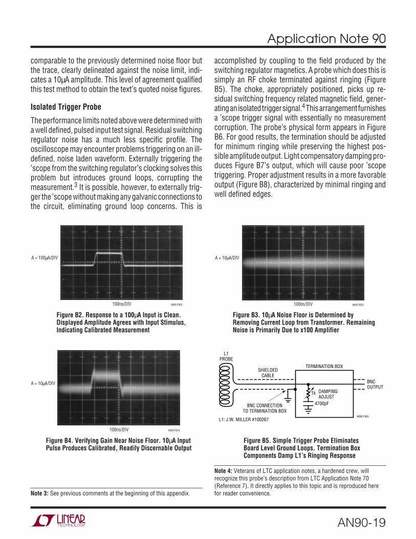
comparable to the previously determined noise floor butthe trace, clearly delineated against the noise limit, indi-cates a 10µA amplitude. This level of agreement qualifiedthis test method to obtain the text’s quoted noise figures.
Isolated Trigger Probe
The performance limits noted above were determined witha well defined, pulsed input test signal. Residual switchingregulator noise has a much less specific profile. Theoscilloscope may encounter problems triggering on an ill-defined, noise laden waveform. Externally triggering the’scope from the switching regulator’s clocking solves thisproblem but introduces ground loops, corrupting themeasurement.3 It is possible, however, to externally trig-ger the ’scope without making any galvanic connections tothe circuit, eliminating ground loop concerns. This is
accomplished by coupling to the field produced by theswitching regulator magnetics. A probe which does this issimply an RF choke terminated against ringing (FigureB5). The choke, appropriately positioned, picks up re-sidual switching frequency related magnetic field, gener-ating an isolated trigger signal.4 This arrangement furnishesa ’scope trigger signal with essentially no measurementcorruption. The probe’s physical form appears in FigureB6. For good results, the termination should be adjustedfor minimum ringing while preserving the highest pos-sible amplitude output. Light compensatory damping pro-duces Figure B7’s output, which will cause poor ’scopetriggering. Proper adjustment results in a more favorableoutput (Figure B8), characterized by minimal ringing andwell defined edges.
Figure B2. Response to a 100µA Input is Clean.Displayed Amplitude Agrees with Input Stimulus,Indicating Calibrated Measurement
100ns/DIV AN90 FB02
A = 100µA/DIV
1k
4700pF
L1: J.W. MILLER #100267AN90 FB05
TERMINATION BOXSHIELDED
CABLE
L1PROBE
BNC CONNECTIONTO TERMINATION BOX
DAMPINGADJUST
BNCOUTPUT
Figure B3. 10µA Noise Floor is Determined byRemoving Current Loop from Transformer. RemainingNoise is Primarily Due to x100 Amplifier
100ns/DIV AN90 FB03
A = 10µA/DIV
Figure B4. Verifying Gain Near Noise Floor. 10µA InputPulse Produces Calibrated, Readily Discernable Output
100ns/DIV AN90 FB04
A = 10µA/DIV
Figure B5. Simple Trigger Probe EliminatesBoard Level Ground Loops. Termination BoxComponents Damp L1’s Ringing Response
Note 4: Veterans of LTC application notes, a hardened crew, willrecognize this probe’s description from LTC Application Note 70(Reference 7). It directly applies to this topic and is reproduced herefor reader convenience.Note 3: See previous comments at the beginning of this appendix.

Application Note 90
AN90-20
Trigger Probe Amplifier
The field around the switching magnetics is small and maynot be adequate to reliably trigger some oscilloscopes. Insuch cases, Figure B9’s trigger probe amplifier is useful.It uses an adaptive triggering scheme to compensate forvariations in probe output amplitude. A stable 5V triggeroutput is maintained over a 50:1 probe output range. A1,operating at a gain of 100, provides wideband AC gain. Theoutput of this stage biases a 2-way peak detector (Q1through Q4). The maximum peak is stored in Q2’s emittercapacitor, while the minimum excursion is retained in Q4’semitter capacitor. The DC value of the midpoint of A1’s
output signal appears at the junction of the 500pF capaci-tor and the 3MΩ units. This point always sits midwaybetween the signal’s excursions, regardless of absoluteamplitude. This signal-adaptive voltage is buffered by A2to set the trigger voltage at the LT1394’s positive input.The LT1394’s negative input is biased directly from A1’soutput. The LT1394’s output, the circuit’s trigger output,is unaffected by >50:1 signal amplitude variations. Anx100 analog output is available at A1.
Figure B10 shows the circuit’s digital output (trace B)responding to the amplified probe signal at A1 (trace A).
Figure B6. The Trigger Probe and Termination Box. ClipLead Facilitates Positioning Probe, is Electrically Neutral

Application Note 90
AN90-21
5V
–
+A1
LT1227
–
+A2
LT1006
5V
5V
5V
DIGITALTRIGGEROUT BNCTO ’SCOPE
AN90 FB09
500pF
0.1µF
1k
470Ω
470Ω
750Ω
10Ω
13
2 4
1413
15
56
1210
11
2k
TRIGGER PROBEAND TERMINATION BOX
(SEE FIGURE B5 FOR DETAILS)
10µF
2k
2k+0.1µF
0.1µF
0.005µF
0.005µF
100µF+
Q1, Q2, Q3, Q4 = CA3096 ARRAY: TIE SUBSTRATE (PIN 16) TO GROUND= 1N4148
–
+
LT1394
Q1 Q2
Q3 Q4
3M
50Ω
3M
ANALOG BNC OUTPUT
Figure B7. Misadjusted Termination Causes InadequateDamping. Unstable Oscilloscope Triggering May Result
10µs/DIV AN90 FB07
10mV/DIV
Figure B8. Properly Adjusted TerminationMinimizes Ringing with Small Amplitude Penalty
10µs/DIV AN90 FB08
10mV/DIV
Figure B9. Trigger Probe Amplifier Has Analog and Digital Outputs. AdaptiveThreshold Maintains Digital Output over 50:1 Probe Signal Variations
Figure B10. Trigger Probe Amplifier Analog(Trace A) and Digital (Trace B) Outputs
10µs/DIV (UNCALIB) AN90 FB10
A = 1V/DIVAC COUPLED
B = 5V/DIV

Application Note 90
AN90-22
APPENDIX C
NOTES ON CURRENT PROBES ANDNOISE MEASUREMENT
Appendix B explained current probes advantages in switch-ing regulator related current noise measurement. Theirminimally invasive nature eases connection parasitics,enhancing measurement fidelity. Different combinationsof current probes and amplifiers provide varying degreesof performance and convenience. Figure C1 summarizescharacteristics for two probes and applicable amplifiers.In general, the noise floor uncertainties of the convenientsplit core types are compromised by their construction.The closed core probes are less noisy and some typeshave inherently higher gain, a distinct advantage. A labo-ratory based comparison is revealing.
Figure C2 shows the CT-1 (closed core)-HP461A combi-nation responding to a 100µA pulsed input. The waveformis clearly outlined, with pulse top and bottom trace thick-ening deriving from the noise floor.1 Figure C3, taken withthe same input, is degraded. The split core P6022-Pre-amble 1855 combination used has much greater noise.The decreased performance is almost entirely due to thesplit core probe’s construction.
In closing, it is worthwhile noting that Hall element stabi-lized current probes (e.g., Tektronix AM503, P6042) arenot suitable for low level measurement. The Hall devicebased flux nulling loop extends probe response to DC butintroduces ≈300µA of noise.
Note 1: Diehard curmudgeons still using high quality analogoscillscopes routinely discern noise presence due to trace thickening.Those stuck with modern instruments routinely view thick, noisytraces.
NOISECURRENT FLOOR
PROBE AMPLIFIER (100 MHz BW) COMMENTS
Tektronix Preamble 100µA Split Core is Convenient to Use but Sensitivity is Low,P6022 1855 Resulting in Relatively High Overall Noise Floor
(1mV/mA) (1MΩ)
Tektronix Hewlett-Packard 15µA Probe’s Higher Gain Accounts for Most Noise Floor Reduction—CT-1 461A 50Ω Input Amplifier Provides Some Additional Benefit.
(5mV/mA) (50Ω) Closed Core Probe Requires Breaking Conductor to Make Measurement
Figure C1. Recommended Instrumentation for Current NoiseMeasurement. Split Core “Current Probe” is Convenient;Closed Core Provides Higher Gain and Lower Noise

Application Note 90
AN90-23
Figure C2. CT-1/HP-461A Combination ClearlyDisplays a 100µA Pulse Train. Noise Floor CausesSlight Pulse Top and Bottom Trace Thickening
500ns/DIV
A = 100µA/DIV
Figure C3. P6022/Preamble 1855 Presentationof Previous Figure’s Waveform Has DegradedSignal-to-Noise Performance. Split Core“Current Probe” Convenience NecessitatesMeasurement Fidelity Compromise
500ns/DIV
A = 100µA/DIV
Information furnished by Linear Technology Corporation is believed to be accurate and reliable.However, no responsibility is assumed for its use. Linear Technology Corporation makes no represen-tation that the interconnection of its circuits as described herein will not infringe on existing patent rights.

Application Note 90
AN90-24Linear Technology Corporation1630 McCarthy Blvd., Milpitas, CA 95035-7417(408) 432-1900 FAX: (408) 434-0507 www.linear.com LINEAR TECHNOLOGY CORPORATION 2002
an90f LT/TP 0402 2K • PRINTED IN USA