CSET 4650 Field Programmable Logic Devices Dan Solarek Antifuse-Based FPGAs: Actel & QuickLogic.
38
CSET 4650 CSET 4650 Field Programmable Logic Devices Field Programmable Logic Devices Dan Solarek Dan Solarek Antifuse-Based Antifuse-Based FPGAs: FPGAs: Actel & QuickLogic Actel & QuickLogic
-
Upload
primrose-holt -
Category
Documents
-
view
233 -
download
6
Transcript of CSET 4650 Field Programmable Logic Devices Dan Solarek Antifuse-Based FPGAs: Actel & QuickLogic.
CSET 4650 CSET 4650 Field Programmable Logic DevicesField Programmable Logic Devices
Dan SolarekDan SolarekDan SolarekDan Solarek
Antifuse-Based FPGAs:Antifuse-Based FPGAs:Actel & QuickLogicActel & QuickLogic
2
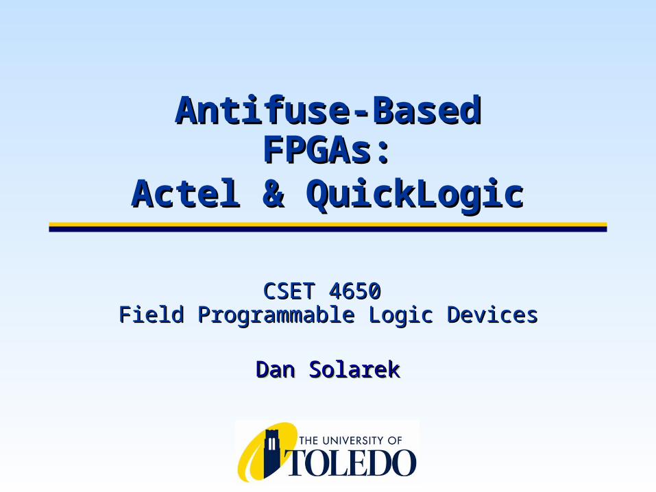
FPGA Design FlowFPGA Design Flow
HDL-based FPGA design flow, as shown at right, increases productivity by allowing you to work at higher levels of abstraction — the register-transfer level instead of the Boolean logic (gate) level.Central to HDL-based design and the increased size of FPGAs are two strategically important tools:
simulation for design verification andsynthesis for automatic implementation of the RTL design to the gate-level (FPGA place and route level).
3
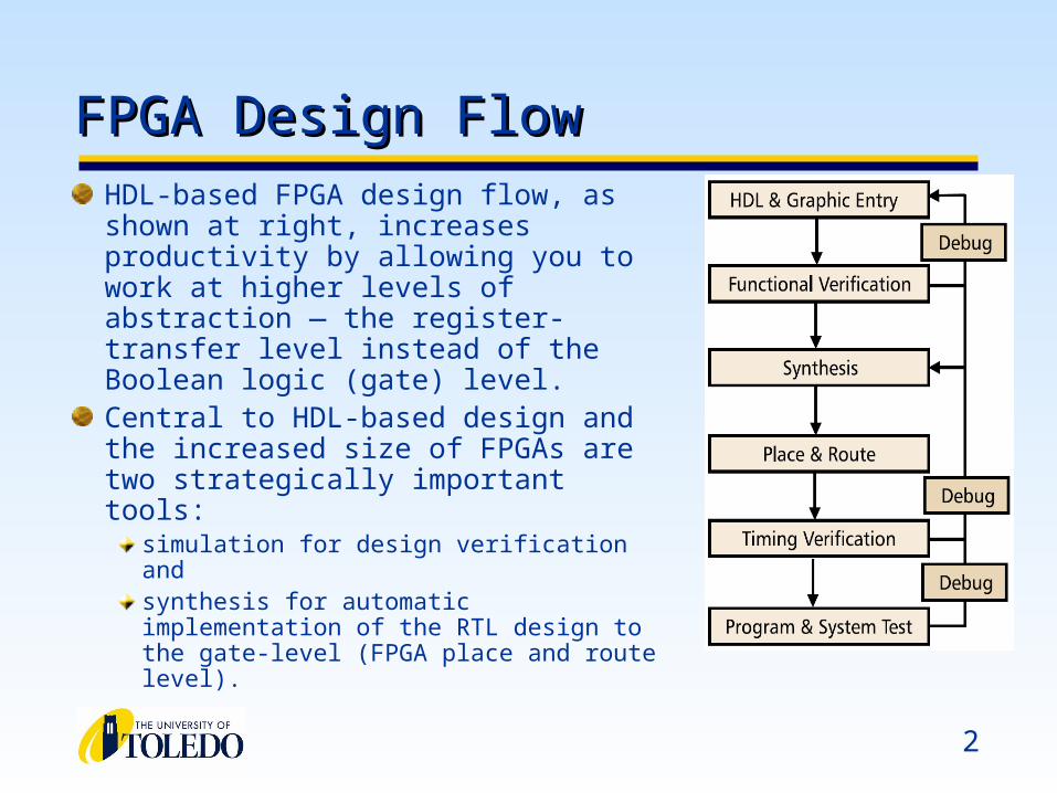
FPGA Design FlowFPGA Design Flow
This flowchart shows a variation This flowchart shows a variation of the FPGA design flowof the FPGA design flow
ISE software, as well as similar ISE software, as well as similar software from other vendors, software from other vendors, may offer several tools at each may offer several tools at each step – not all of which are step – not all of which are essential to use for each designessential to use for each design
Learn the generalized flow as a Learn the generalized flow as a guide to your design effortsguide to your design efforts
4
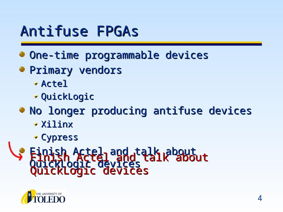
Antifuse FPGAsAntifuse FPGAs
One-time programmable devicesOne-time programmable devices
Primary vendorsPrimary vendorsActelActel
QuickLogicQuickLogic
No longer producing antifuse devicesNo longer producing antifuse devicesXilinxXilinx
CypressCypress
Finish Actel and talk about QuickLogic devicesFinish Actel and talk about QuickLogic devicesFinish Actel and talk about QuickLogic devicesFinish Actel and talk about QuickLogic devices
5
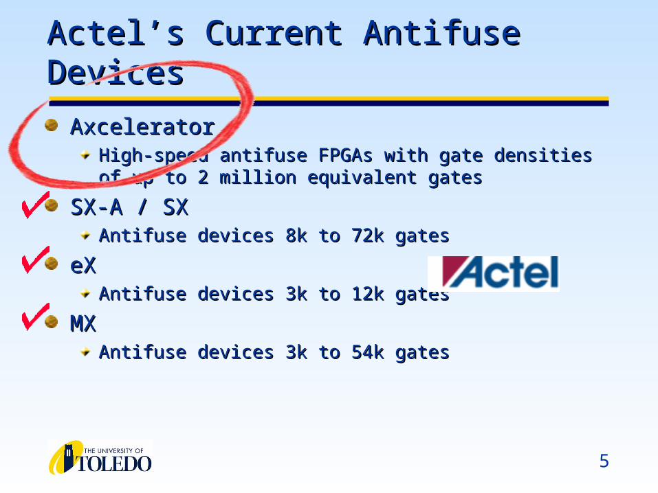
Actel’s Current Antifuse DevicesActel’s Current Antifuse Devices
Axcelerator Axcelerator High-speed antifuse FPGAs with gate densities of up to 2 million High-speed antifuse FPGAs with gate densities of up to 2 million equivalent gates equivalent gates
SX-A / SX SX-A / SX Antifuse devices 8k to 72k gates Antifuse devices 8k to 72k gates
eX eX Antifuse devices 3k to 12k gates Antifuse devices 3k to 12k gates
MX MX Antifuse devices 3k to 54k gatesAntifuse devices 3k to 54k gates
6
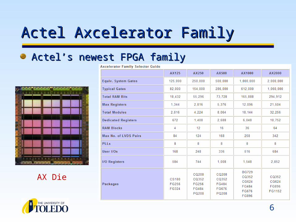
Actel Axcelerator FamilyActel Axcelerator Family
Actel’s newest FPGA familyActel’s newest FPGA family
AX Die
7
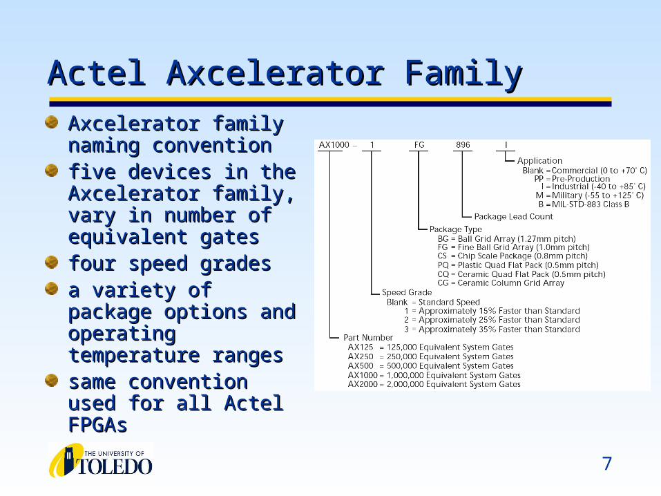
Actel Axcelerator FamilyActel Axcelerator Family
Axcelerator family Axcelerator family naming conventionnaming conventionfive devices in the five devices in the Axcelerator family, vary Axcelerator family, vary in number of equivalent in number of equivalent gatesgatesfour speed gradesfour speed gradesa variety of package a variety of package options and operating options and operating temperature rangestemperature rangessame convention used for same convention used for all Actel FPGAsall Actel FPGAs
8
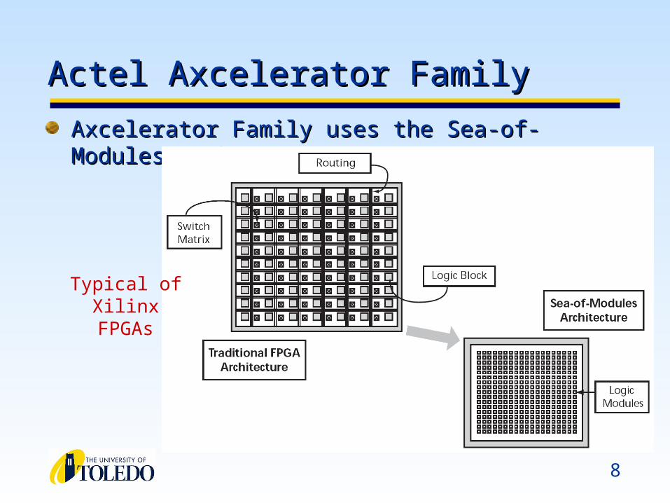
Actel Axcelerator FamilyActel Axcelerator Family
Axcelerator Family uses the Sea-of-Modules architectureAxcelerator Family uses the Sea-of-Modules architecture
Typical of Xilinx FPGAs
9
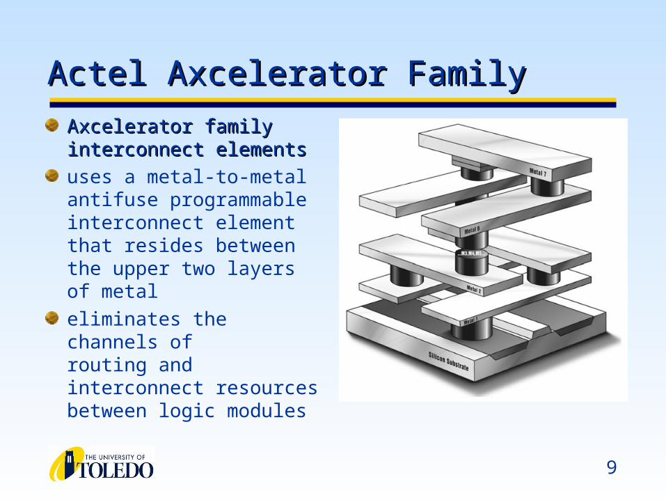
Actel Axcelerator FamilyActel Axcelerator Family
Axcelerator family Axcelerator family interconnect elementsinterconnect elements
uses a metal-to-metal antifuse programmable interconnect element that resides between the upper two layers of metal
eliminates the channels of routing and interconnect resources between logic modules
10
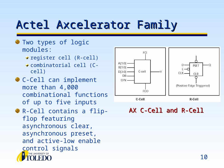
Actel Axcelerator FamilyActel Axcelerator Family
Two types of logic modules:register cell (R-cell)
combinatorial cell (C-cell)
C-Cell can implement more than 4,000 combinational functions of up to five inputs
R-Cell contains a flip-flop featuring asynchronous clear, asynchronous preset, and active-low enable control signals
AX C-Cell and R-CellAX C-Cell and R-Cell
11
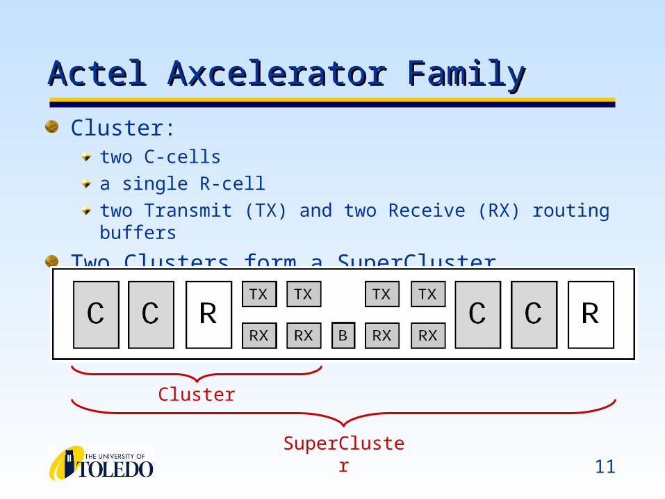
Actel Axcelerator FamilyActel Axcelerator Family
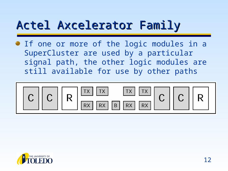
Cluster:two C-cells
a single R-cell
two Transmit (TX) and two Receive (RX) routing buffers
Two Clusters form a SuperCluster
Cluster
SuperCluster
12
Actel Axcelerator FamilyActel Axcelerator Family
If one or more of the logic modules in a SuperCluster are used by a particular signal path, the other logic modules are still available for use by other paths

13
Actel Axcelerator FamilyActel Axcelerator Family
The C–C–R pattern of the AX Cluster enables efficient implementation (minimum delay) of two-bit carry logic for improved arithmetic performance
14
Actel Axcelerator FamilyActel Axcelerator Family
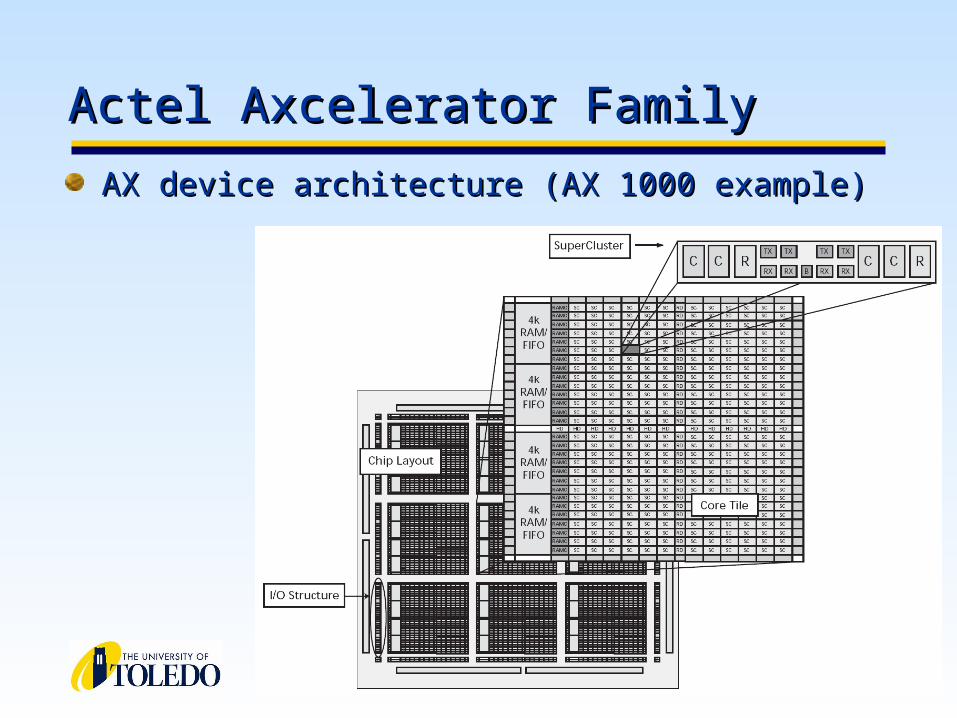
AX device architecture (AX 1000 example)AX device architecture (AX 1000 example)
15
Actel Axcelerator FamilyActel Axcelerator Family
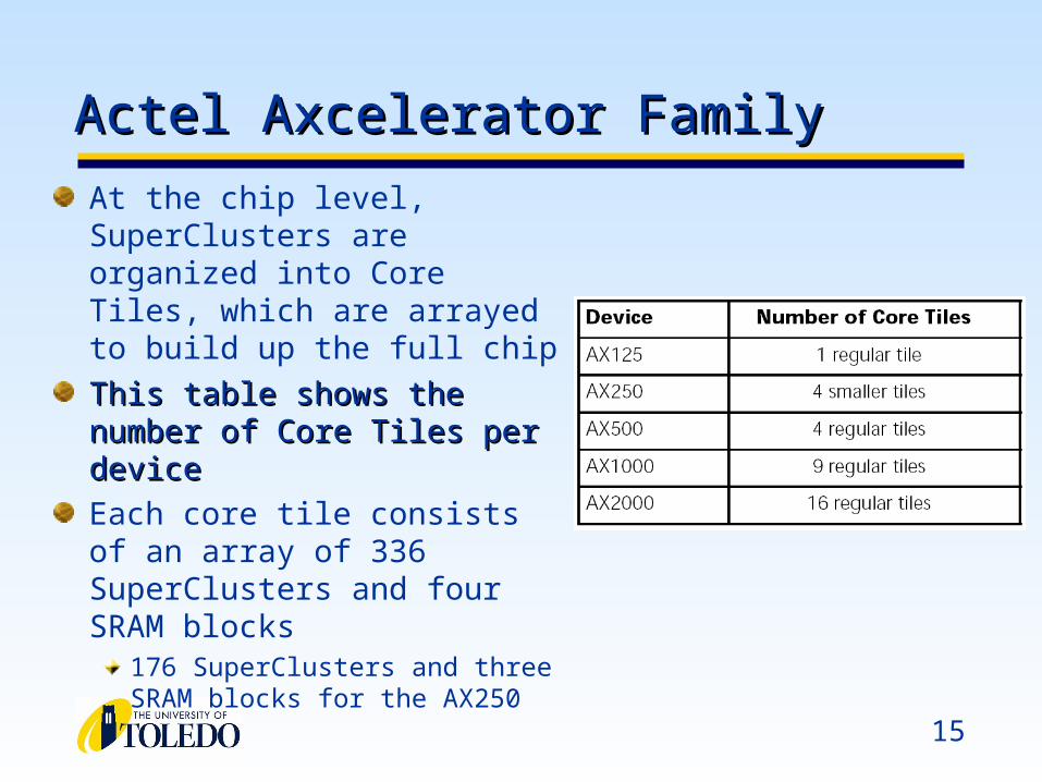
At the chip level, SuperClusters are organized into Core Tiles, which are arrayed to build up the full chip
This table shows the number of This table shows the number of Core Tiles per deviceCore Tiles per device
Each core tile consists of an array of 336 SuperClusters and four SRAM blocks
176 SuperClusters and three SRAM blocks for the AX250
16
Actel Axcelerator FamilyActel Axcelerator Family
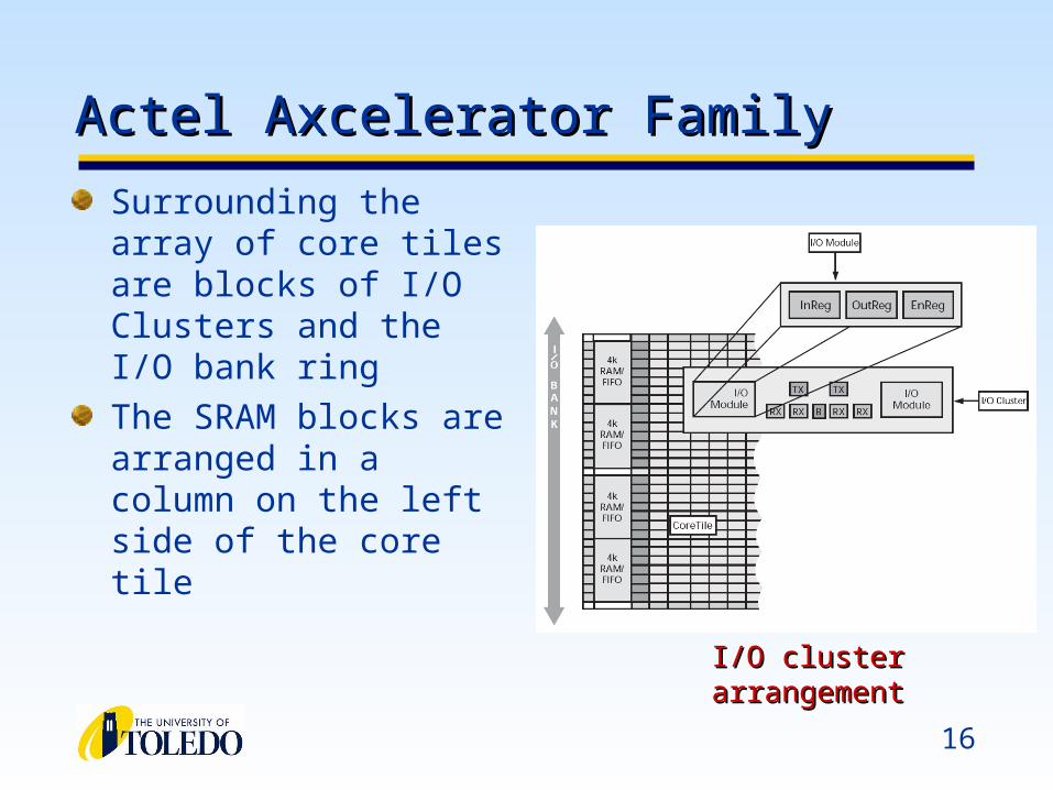
Surrounding the array of core tiles are blocks of I/O Clusters and the I/O bank ring
The SRAM blocks are arranged in a column on the left side of the core tile
I/O cluster arrangementI/O cluster arrangement
17
Actel Axcelerator FamilyActel Axcelerator Family
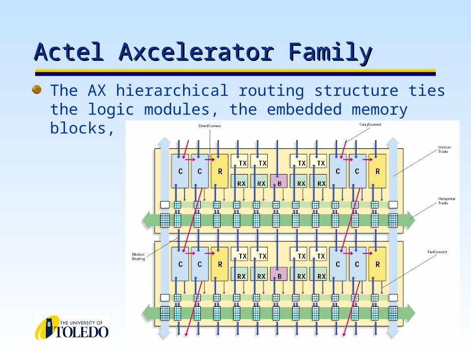
The AX hierarchical routing structure ties the logic modules, the embedded memory blocks, and the I/O modules together
18
Actel Axcelerator FamilyActel Axcelerator Family
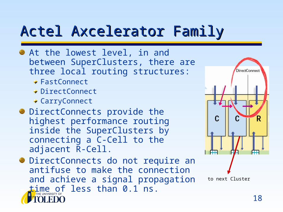
At the lowest level, in and between SuperClusters, there are three local routing structures:
FastConnect DirectConnectCarryConnect
DirectConnects provide the highest performance routing inside the SuperClusters by connecting a C-Cell to the adjacent R-Cell. DirectConnects do not require an antifuse to make the connection and achieve a signal propagation time of less than 0.1 ns. to next Cluster
19
Actel Axcelerator FamilyActel Axcelerator Family
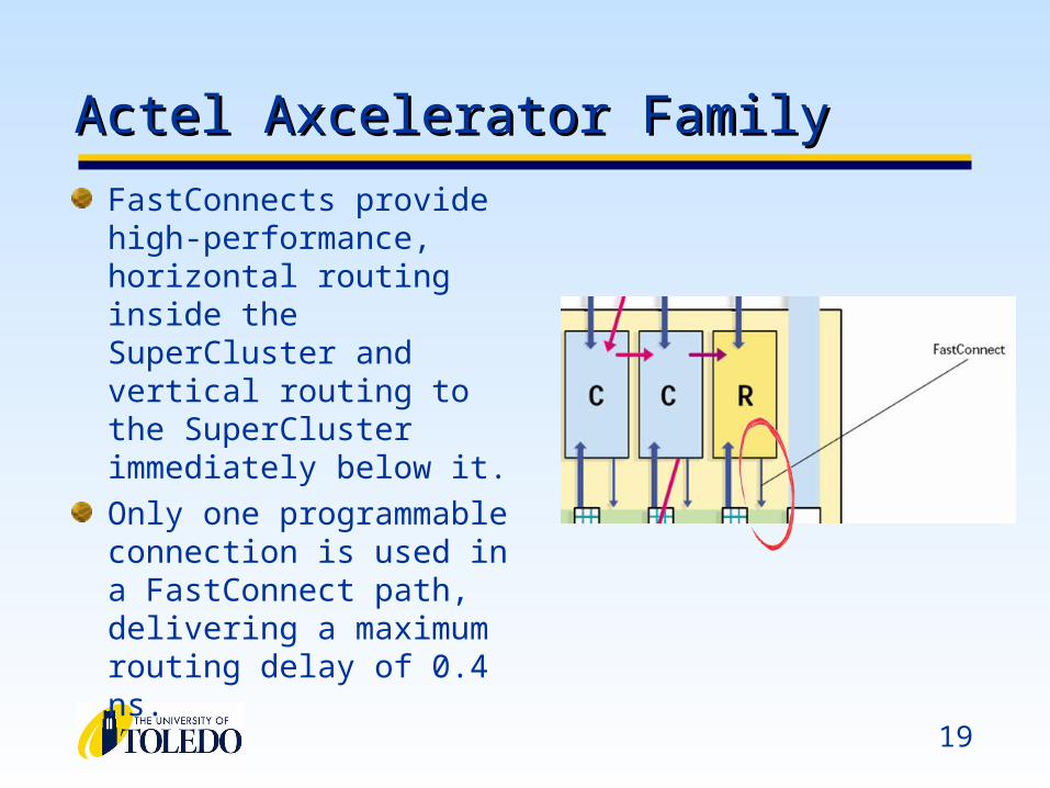
FastConnects provide high-performance, horizontal routing inside the SuperCluster and vertical routing to the SuperCluster immediately below it.
Only one programmable connection is used in a FastConnect path, delivering a maximum routing delay of 0.4 ns.
20
Actel Axcelerator FamilyActel Axcelerator Family
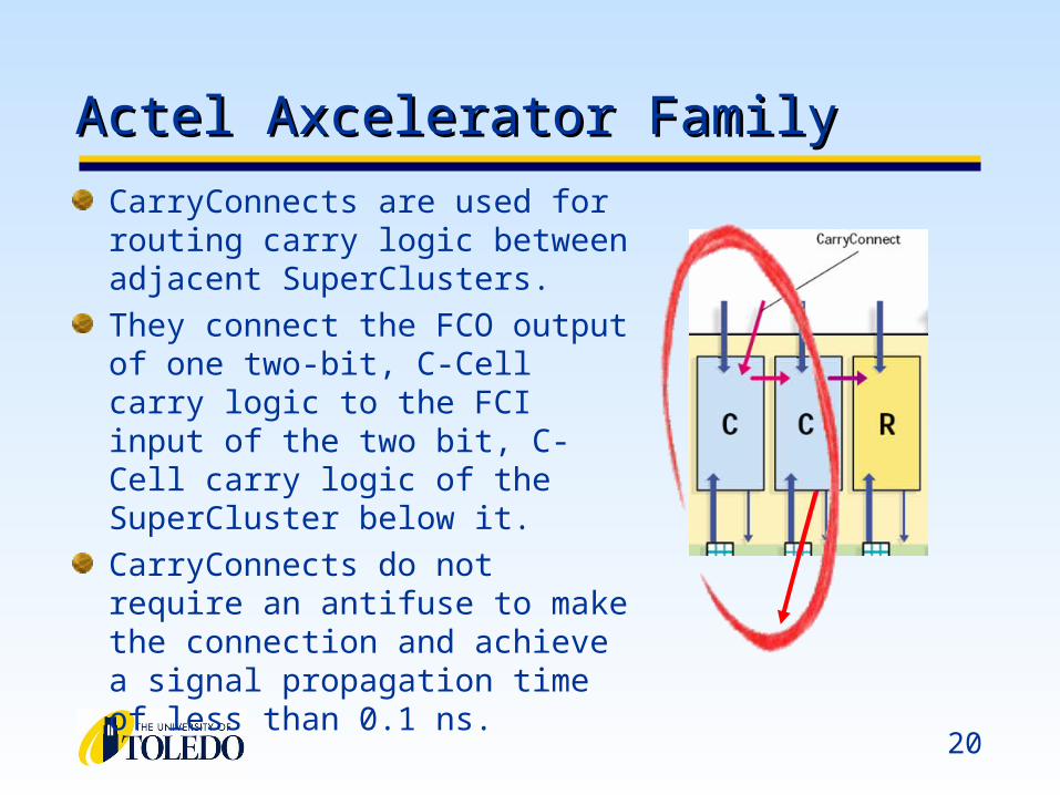
CarryConnects are used for routing carry logic between adjacent SuperClusters.
They connect the FCO output of one two-bit, C-Cell carry logic to the FCI input of the two bit, C-Cell carry logic of the SuperCluster below it.
CarryConnects do not require an antifuse to make the connection and achieve a signal propagation time of less than 0.1 ns.
21
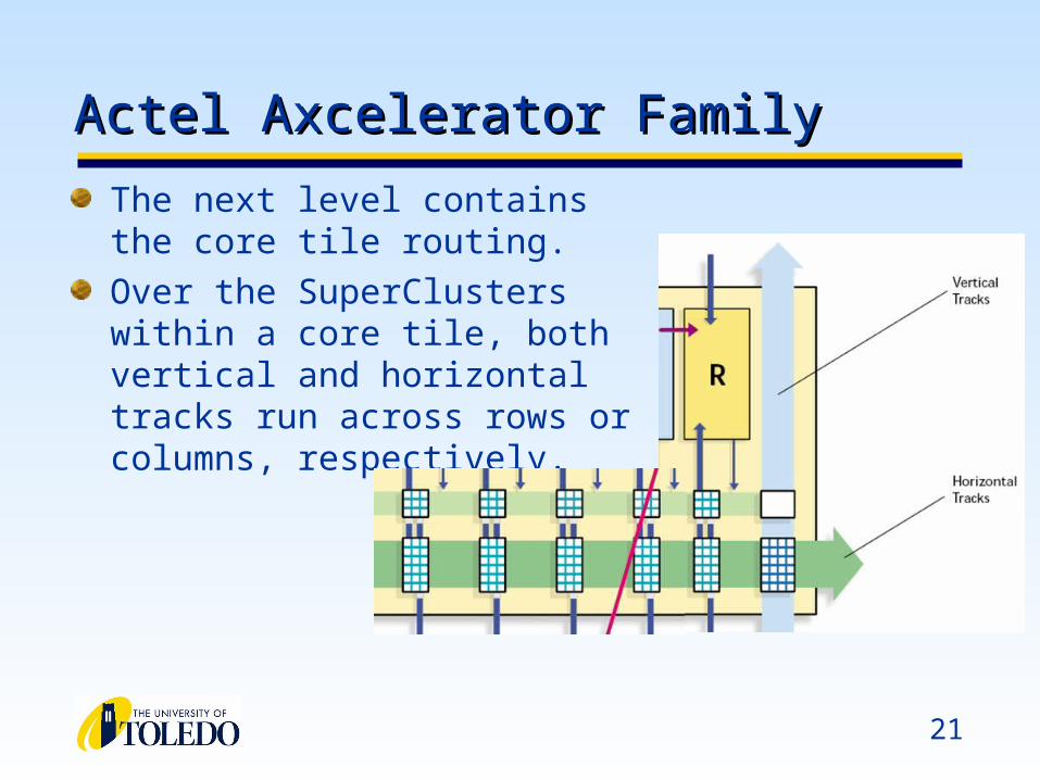
Actel Axcelerator FamilyActel Axcelerator Family
The next level contains the core tile routing.
Over the SuperClusters within a core tile, both vertical and horizontal tracks run across rows or columns, respectively.

22
Actel Axcelerator FamilyActel Axcelerator Family
At the chip level, vertical and horizontal tracks extend across the full length of the device, both north-to-south and east-to-west.
These tracks are composed of highway routing that extend the entire length of the device (segmented at core tile boundaries) as well as segmented routing of varying lengths.
23
QuickLogic DevicesQuickLogic Devices
24
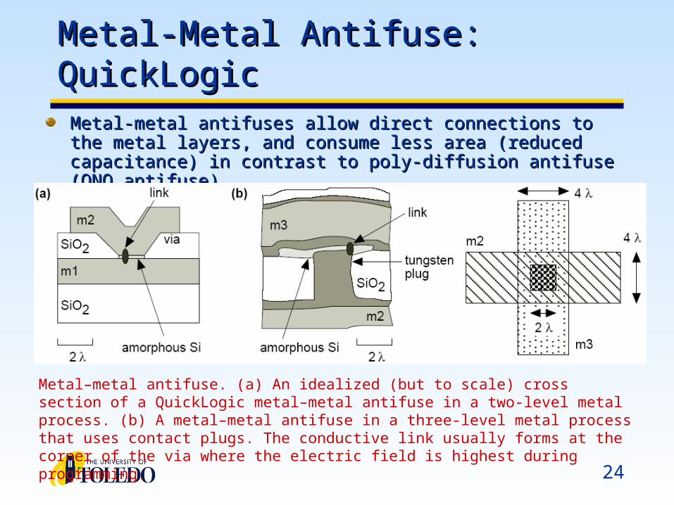
Metal-Metal Antifuse: QuickLogicMetal-Metal Antifuse: QuickLogicMetal-metal antifuses allow direct connections to the metal layers, and Metal-metal antifuses allow direct connections to the metal layers, and consume less area (reduced capacitance) in contrast to poly-diffusion consume less area (reduced capacitance) in contrast to poly-diffusion antifuse (ONO antifuse).antifuse (ONO antifuse).
Metal–metal antifuse. (a) An idealized (but to scale) cross section of a QuickLogic metal–metal antifuse in a two-level metal process. (b) A metal–metal antifuse in a three-level metal process that uses contact plugs. The conductive link usually forms at the corner of the via where the electric field is highest during programming.
25
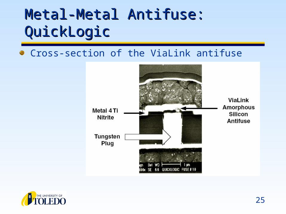
Metal-Metal Antifuse: QuickLogicMetal-Metal Antifuse: QuickLogic
Cross-section of the ViaLink antifuse
26
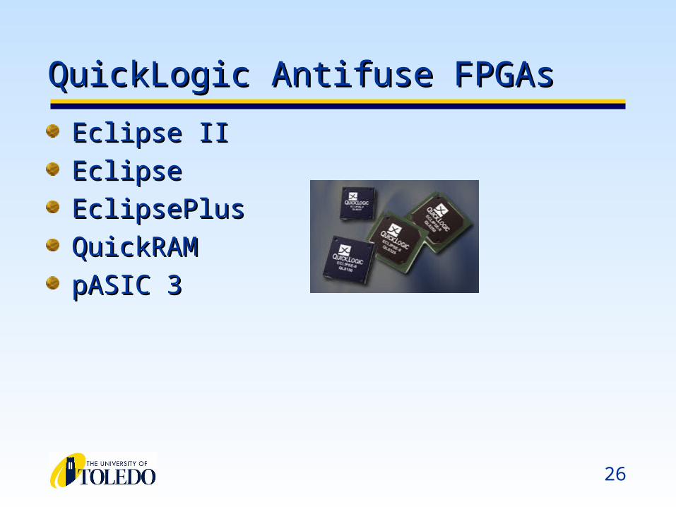
QuickLogic Antifuse FPGAsQuickLogic Antifuse FPGAs
Eclipse IIEclipse II
EclipseEclipse
EclipsePlusEclipsePlus
QuickRAMQuickRAM
pASIC 3pASIC 3
27
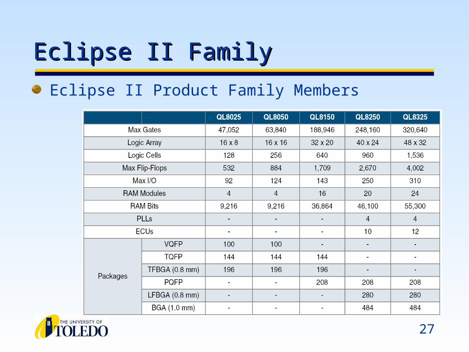
Eclipse II FamilyEclipse II Family
Eclipse II Product Family Members
28
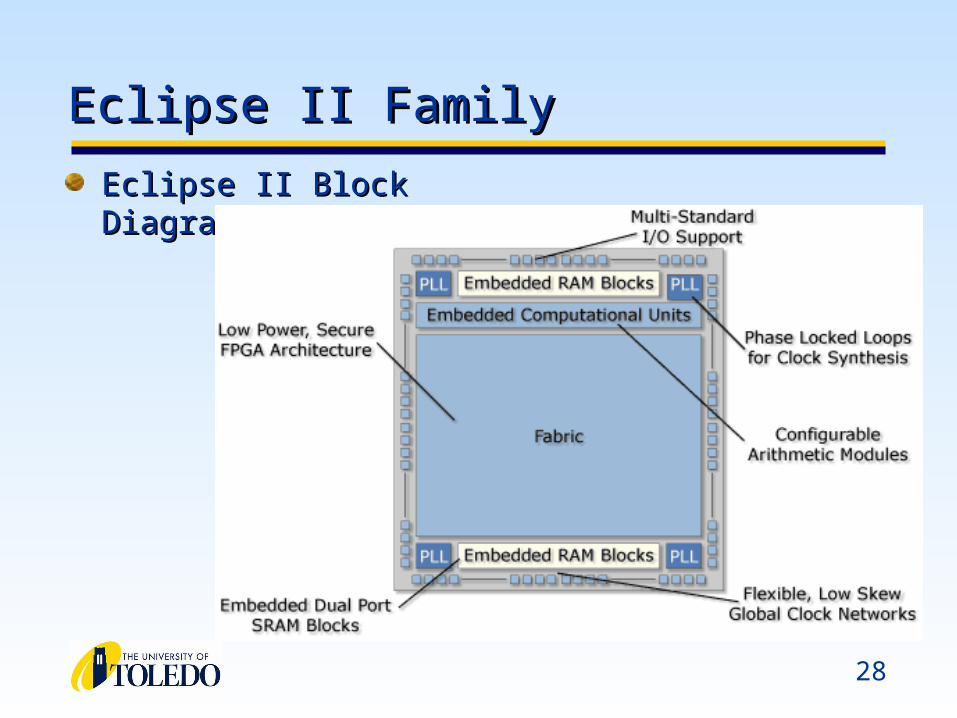
Eclipse II FamilyEclipse II Family
Eclipse II Block DiagramEclipse II Block Diagram
29
Eclipse II FamilyEclipse II Family
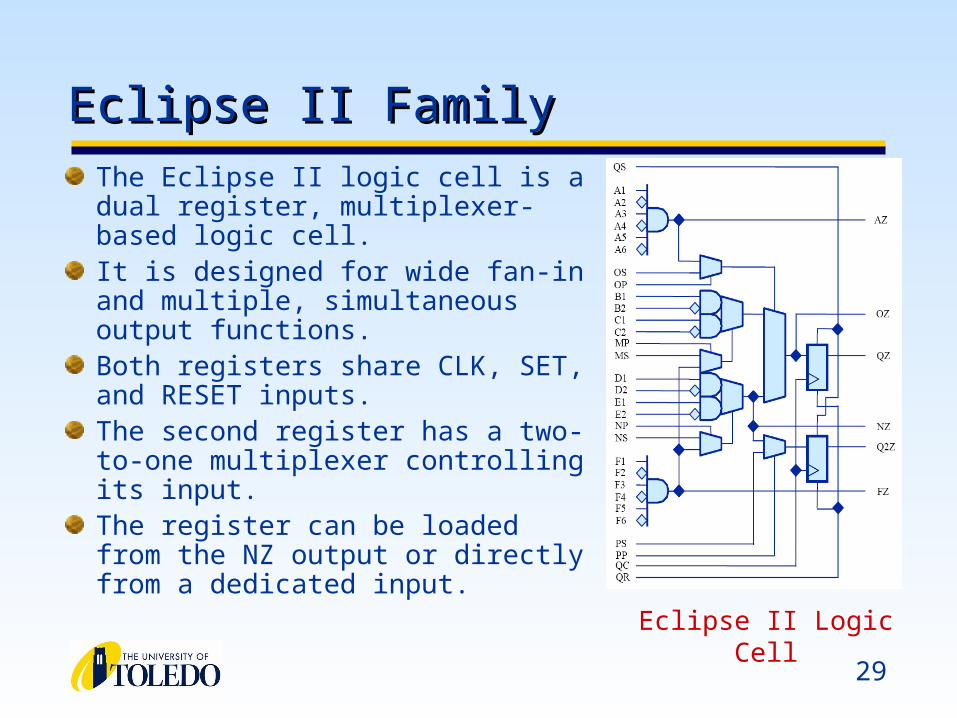
The Eclipse II logic cell is a dual register, multiplexer-based logic cell. It is designed for wide fan-in and multiple, simultaneous output functions. Both registers share CLK, SET, and RESET inputs. The second register has a two-to-one multiplexer controlling its input. The register can be loaded from the NZ output or directly from a dedicated input.
Eclipse II Logic Cell
30
Eclipse II FamilyEclipse II Family
The complete logic cell consists of two six-input AND gates, The complete logic cell consists of two six-input AND gates, four two-input AND gates, seven two-to-one multiplexers, four two-input AND gates, seven two-to-one multiplexers, and two D flip-flops with asynchronous SET and RESET and two D flip-flops with asynchronous SET and RESET controls. controls. The cell has a fan-in of 30 (including register control lines), The cell has a fan-in of 30 (including register control lines), fits a wide range of functions with up to 17 simultaneous fits a wide range of functions with up to 17 simultaneous inputs, and has six outputs (four combinational and two inputs, and has six outputs (four combinational and two registered). registered). The high logic capacity and fan-in of the logic cell The high logic capacity and fan-in of the logic cell accommodates many user functions with a single level of accommodates many user functions with a single level of logic delay while other architectures require two or more logic delay while other architectures require two or more levels of delay.levels of delay.
31
Eclipse II FamilyEclipse II Family
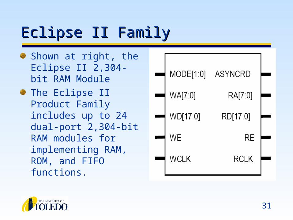
Shown at right, the Eclipse II 2,304-bit RAM Module
The Eclipse II Product Family includes up to 24 dual-port 2,304-bit RAM modules for implementing RAM, ROM, and FIFO functions.
32
Eclipse II FamilyEclipse II Family
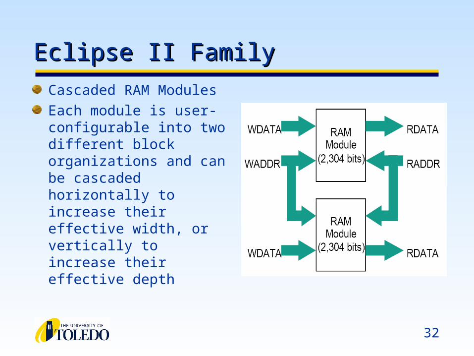
Cascaded RAM Modules
Each module is user-configurable into two different block organizations and can be cascaded horizontally to increase their effective width, or vertically to increase their effective depth
33
Eclipse II FamilyEclipse II Family
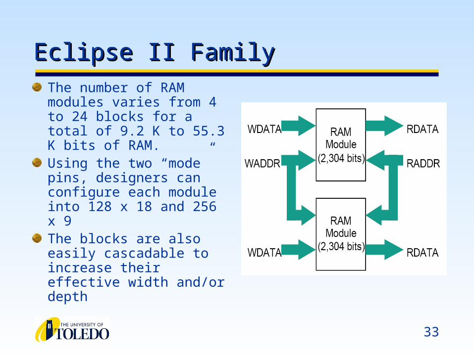
The number of RAM modules varies from 4 to 24 blocks for a total of 9.2 K to 55.3 K bits of RAM.Using the two “mode” pins, designers can configure each module into 128 x 18 and 256 x 9The blocks are also easily cascadable to increase their effective width and/or depth
34
Eclipse II FamilyEclipse II Family
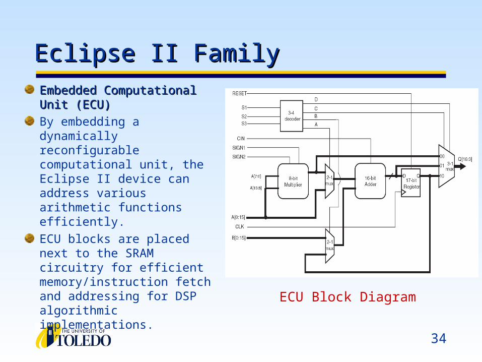
Embedded Computational Embedded Computational Unit (ECU)Unit (ECU)
By embedding a dynamically reconfigurable computational unit, the Eclipse II device can address various arithmetic functions efficiently.
ECU blocks are placed next to the SRAM circuitry for efficient memory/instruction fetch and addressing for DSP algorithmic implementations. ECU Block Diagram
35
Eclipse II FamilyEclipse II Family
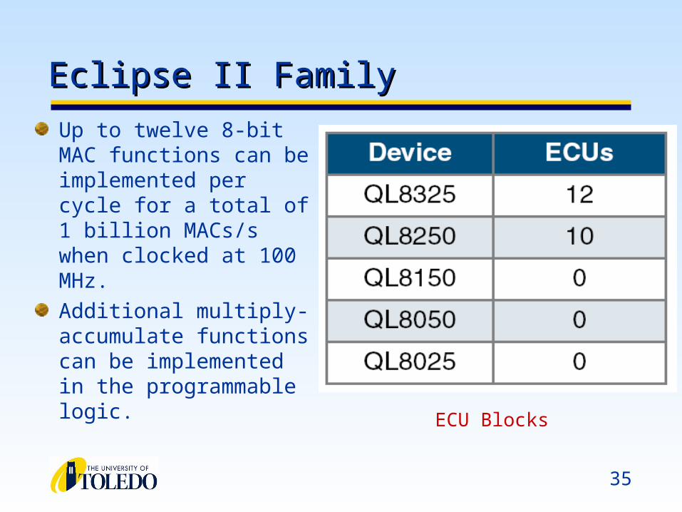
Up to twelve 8-bit MAC functions can be implemented per cycle for a total of 1 billion MACs/s when clocked at 100 MHz.
Additional multiply-accumulate functions can be implemented in the programmable logic.
ECU Blocks
36
Eclipse II FamilyEclipse II Family
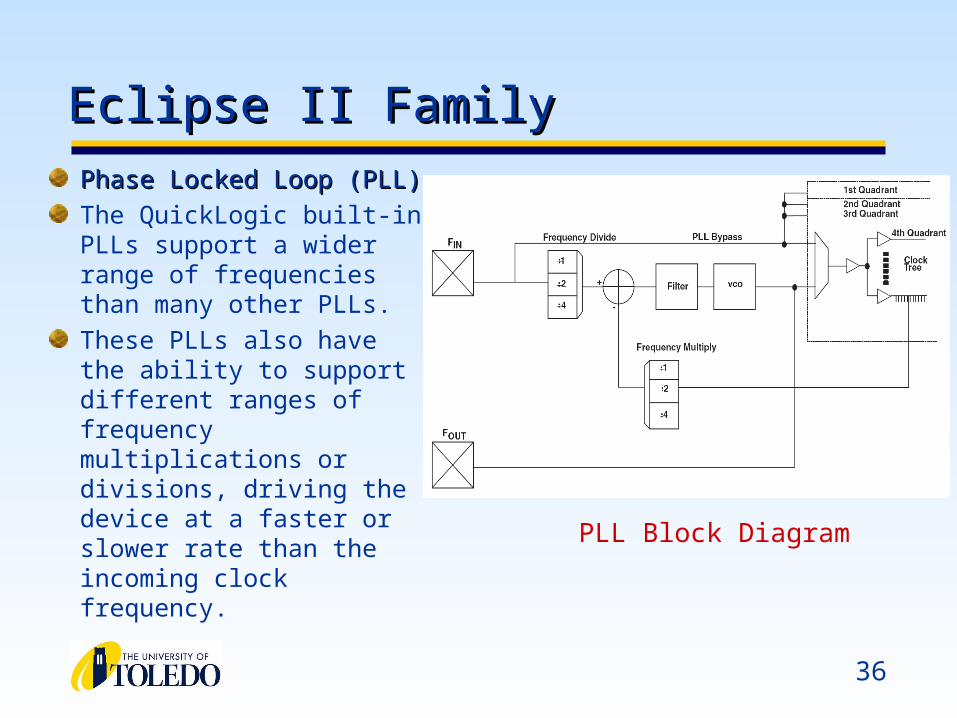
Phase Locked Loop (PLL)Phase Locked Loop (PLL)
The QuickLogic built-in PLLs support a wider range of frequencies than many other PLLs.
These PLLs also have the ability to support different ranges of frequency multiplications or divisions, driving the device at a faster or slower rate than the incoming clock frequency.
PLL Block Diagram
37
Eclipse II FamilyEclipse II Family
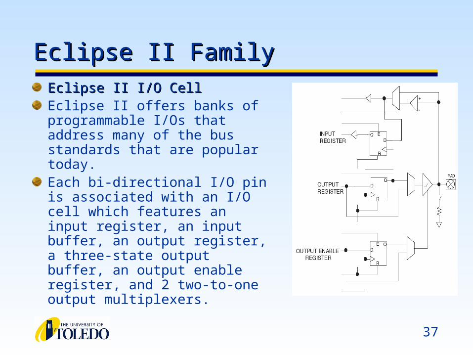
Eclipse II I/O CellEclipse II I/O CellEclipse II offers banks of programmable I/Os that address many of the bus standards that are popular today.Each bi-directional I/O pin is associated with an I/O cell which features an input register, an input buffer, an output register, a three-state output buffer, an output enable register, and 2 two-to-one output multiplexers.
38
AssignmentAssignment
Read over the datasheets for:Read over the datasheets for:EclipseEclipse
EclipsePlusEclipsePlus
QuickRAMQuickRAM
pASIC 3pASIC 3
Compare the architecture of these to the Eclipse II Compare the architecture of these to the Eclipse II familyfamily
Come to class on Monday prepared to discuss your Come to class on Monday prepared to discuss your findingsfindings