CPEN 315 - Digital System Design Chapter 7 – Registers and Register Transfers Part 1 –...
24
CPEN 315 - Digital System Design Chapter 7 – Registers and Register Transfers Part 1 – Registers, Microoperations and Implementations C. Gerousis © Logic and Computer Design Fundamentals, 4 rd Ed., Mano Prentice Hall Charles Kime & Thomas Kaminski © 2008 Pearson Education, Inc.
-
Upload
dorothy-harned -
Category
Documents
-
view
224 -
download
0
Transcript of CPEN 315 - Digital System Design Chapter 7 – Registers and Register Transfers Part 1 –...

CPEN 315 - Digital System Design
Chapter 7 – Registers and Register TransfersPart 1 – Registers, Microoperations and Implementations
C. Gerousis© Logic and Computer Design Fundamentals, 4rd Ed., Mano
Prentice Hall
Charles Kime & Thomas Kaminski
© 2008 Pearson Education, Inc.

Overview
Part 1 - Registers, Microoperations and Implementations– Registers and load enable– Register transfer operations– Microoperations - arithmetic, logic, and shift– Microoperations on a single register
Multiplexer-based transfers Shift registers
Part 2 - Counters, register cells, buses, & serial operations– Microoperations on single register (continued)– Counters– Register cell design– Multiplexer and bus-based transfers for multiple registers– Serial transfers and microoperations

Registers
Register – a collection of binary storage elements
In theory, a register is sequential logic which can be defined by a state table
More often think of a register as storing a vector of binary values
Frequently used to perform simple data storage and data movement and processing operations
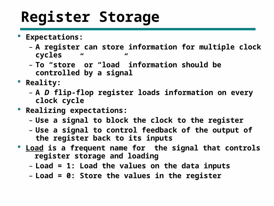
Register Storage Expectations:
– A register can store information for multiple clock cycles– To “store” or “load” information should be controlled by a
signal Reality:
– A D flip-flop register loads information on every clock cycle Realizing expectations:
– Use a signal to block the clock to the register– Use a signal to control feedback of the output of the register
back to its inputs Load is a frequent name for the signal that controls register
storage and loading– Load = 1: Load the values on the data inputs– Load = 0: Store the values in the register

A reliable way to selectively load a register:
– Run the clock continuously, and
– Selectively use a load control to change the register contents.
Example: 2-bit registerwith Load Control:
For Load = 0,loads register contents(hold current values)
For Load = 1,loads input values(load new values)
Hardware more complex,
but free of timing problems
Registers with Load-Controlled Feedback
CD Q
C
D Q
Clock
In0
In1
A1
A0
Y1
Y0
Load
2-to-1 Multiplexers
What is the purpose of the feedback?

Register Transfer Operations
Register Transfer Operations The movement and processing of data stored in
registers Three basic components:
– set of registers– operations– control of operations
Elementary Operations -- load, count, shift, add, bitwise "OR", etc.– Elementary operations called microoperations

Register Notation
Letters and numbers – denotes a register (ex. R2, PC, IR) Parentheses ( ) – denotes a range of register bits (ex. R1(1),
PC(7:0), AR(L)) Arrow () – denotes data transfer (ex. R1 R2, PC(L) R0) Comma – separates parallel operations Brackets [ ] – Specifies a memory address (ex. R0 M[AR],
R3 M[PC] )
15 8 7 0 15 0
PC(H) PC(L) R2

Readregister 1
Readregister 2
Writeregister
Writedata
Registers ALU
Zero
Readdata 1
Readdata 2
Signextend
16 32
Instruction[25–21]
Instruction[20–16]
Instruction[15–0]
ALUresult
Mux
Mux
Shiftleft 2
Instructionregister
PC 0
1
Mux
0
1
Mux
0
1
Mux
0
1A
B 0
1
2
3
ALUOut
Instruction[15–0]
Memorydata
register
Address
Writedata
Memory
MemData
4
Instruction[15–11]
Processor Datapath
IR
MDR
A
B
ALUOut
registerfile

Conditional Transfer
If (K1 =1) then (R2 R1) is shortened to
K1: (R2 R1) where K1 is a control
variable specifying a conditional executionof the microoperation.
R1 R2
K1
Clock
Loadn
Clock
K1Transfer Occurs Here
No Transfers Occur Here

Microoperations
In a digital system microoperations are of four types:– Transfer - move data from one set of registers to another
– Arithmetic - perform arithmetic on data in registers
– Logic - manipulate data or use bitwise logical operations
– Shift - shift data in registers
Arithmetic operations+ Addition– Subtraction* Multiplication/ Division
Logical operations Logical OR Logical AND Logical Exclusive OR Not

Example Microoperations
Add the content of R1 to the content of R2 and place the result in R1.
R1 R1 + R2 Multiply the content of R1 by the content of R6
and place the result in PC. PC R1 * R6 Exclusive OR the content of R1 with the
content of R2 and place the result in R1. R1 R1 R2
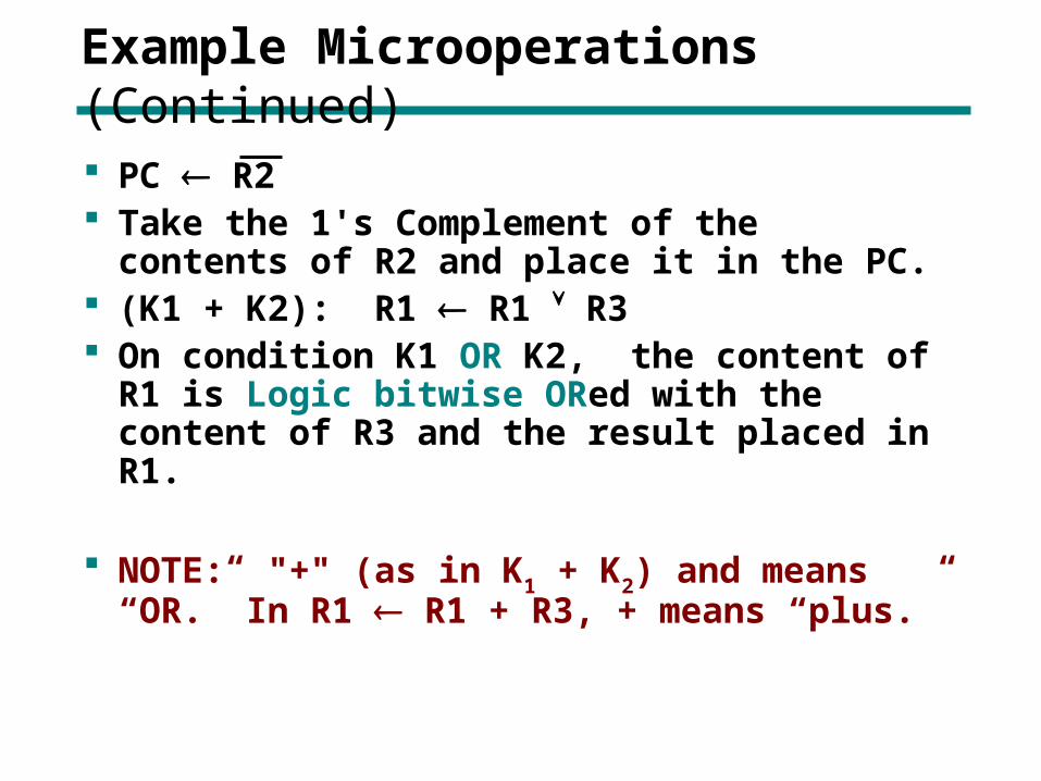
Example Microoperations (Continued)
PC R2 Take the 1's Complement of the contents of R2
and place it in the PC. (K1 + K2): R1 R1 R3 On condition K1 OR K2, the content of R1 is
Logic bitwise ORed with the content of R3 and the result placed in R1.
NOTE: "+" (as in K1 + K2) and means “OR.” In R1 R1 + R3, + means “plus.”
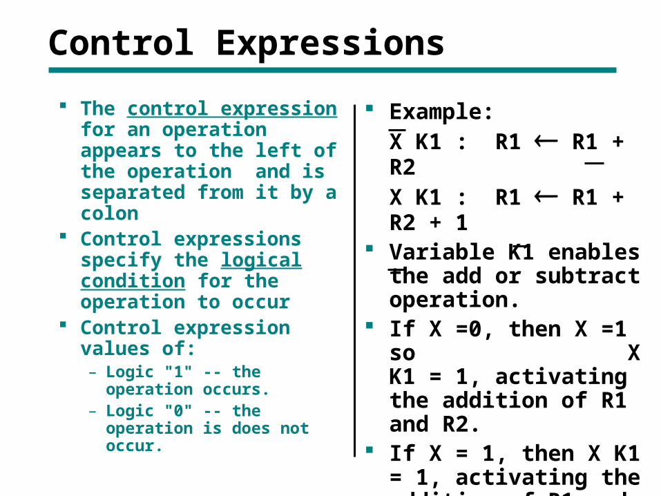
Control Expressions
The control expression for an operation appears to the left of the operation and is separated from it by a colon
Control expressions specify the logical condition for the operation to occur
Control expression values of:– Logic "1" -- the operation
occurs.– Logic "0" -- the operation is
does not occur.
Example:X K1 : R1 R1 + R2
X K1 : R1 R1 + R2 + 1 Variable K1 enables the
add or subtract operation. If X =0, then X =1 so
X K1 = 1, activating the addition of R1 and R2.
If X = 1, then X K1 = 1, activating the addition of R1 and the two's complement of R2 (subtract).
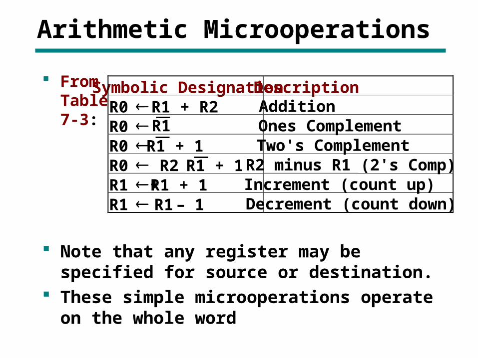
Arithmetic Microoperations
FromTable7-3:
Note that any register may be specified for source or destination.
These simple microoperations operate on the whole word
Symbolic Designation Description R0 R1 + R2 Addition R0 R1 Ones Complement R0 R1 + 1 Two's Complement R0 R2 + R1 + 1 R2 minus R1 (2's Comp) R1 R1 + 1 Increment (count up) R1 R1 – 1 Decrement (count down)

Logical Microoperations
Symbolic Designation
Description
R0 R1 Bitwise NOT
R0 R1 R2 Bitwise OR (sets bits)
R0 R1 R2 Bitwise AND (clears bits)
R0 R1 R2 Bitwise XOR (complements bits)
From Table 7-4:

Logical Microoperations (continued)
Let R1 = 10101010, and R2 = 11110000
Then after the operation, R0 becomes:
R0 Operation
01010101 R0 R1
11111010 R0 R1 R2
10100000 R0 R1 R2
01011010 R0 R1 R2
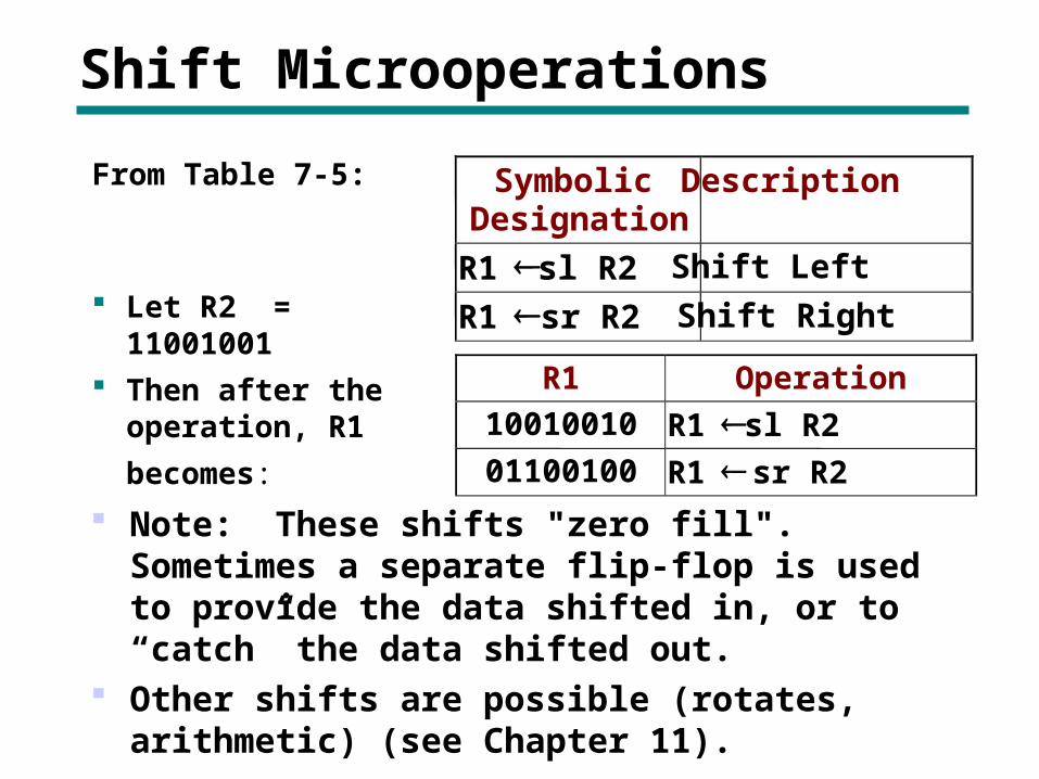
Shift Microoperations
From Table 7-5:
Let R2 = 11001001 Then after the
operation, R1
becomes:
Symbolic Designation
Description
R1 sl R2 Shift Left
R1 sr R2 Shift Right
R1 Operation
10010010 R1 sl R2
01100100 R1 sr R2 Note: These shifts "zero fill". Sometimes a separate
flip-flop is used to provide the data shifted in, or to “catch” the data shifted out.
Other shifts are possible (rotates, arithmetic) (see Chapter 11).

Register Transfer Structures
Multiplexer-Based Transfers - Multiple inputs are selected by a multiplexer dedicated to the register
Bus-Based Transfers - Multiple inputs are selected by a shared multiplexer driving a bus that feeds inputs to multiple registers
Other Transfer Structures - Use multiple multiplexers, multiple buses, and combinations of all the above

Multiplexer-Based Transfers
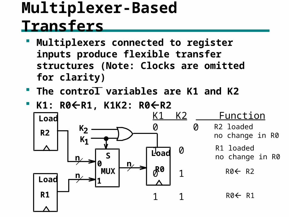
Multiplexer-Based Transfers
Multiplexers connected to register inputs produce flexible transfer structures (Note: Clocks are omitted for clarity)
The control variables are K1 and K2 K1: R0R1, K1K2: R0R2
Load
R0n
MUX
S
K2
0
1
Load
Load
n
n
K1R2
R1
K1 K2 Function0 0 1 0
0 1
1 1
R2 loadedno change in R0
R1 loadedno change in R0
R0 R2
R0 R1

Shift Registers move data laterally within the register toward its MSB or LSB position
Data input, In, is called a serial input or the shift right input.
Data output, Out, is often called the serial output. The vector (A, B, C, Out) is called the parallel output.
data_
Shift Registers
A B C

Serial Shift Registers – Timing Diagram
Q0 Q1 Q2 = Q3

DQ
DQ
A B
CP
SHIFT
IN
DA DB
By adding a mux between each shift register stage, data can be shifted or loaded
If SHIFT is low, A and B are replaced by the data on DA and DB lines, else data shifts right on each clock.
Parallel Load Shift Registers
Next Time... Part 2 - Counters, register cells, buses, & serial
operations– Microoperations on single register (continued)– Counters– Register cell design– Multiplexer and bus-based transfers for multiple
registers– Serial transfers and microoperations