©Copyright by Michael E. Jacob
81
Transcript of ©Copyright by Michael E. Jacob


AN ABSTRACT OF THE THESIS OF
Michael E. Jacob for the degree of
Master of Science in Electrical and Computer Engineering
presented on May 28, 2009.
Title: Ultra Low Capacitance RFIC Probe
Abstract approved:
____________________________________________________
Leonard Forbes
In Radio Frequency Integrated Circuits (RFIC) or high frequency digital
ICs, there is a demand to probe the internal nodes for testing. The ultra low
capacitance RFIC probe presented in his work is a flexible tool for these
applications. The probe utilizes the coupling between a tungsten needle and the
inner conductor of a coaxial cable, forming a capacitor. The ultra low capacitance
of the probe enables low probe loading on the circuit under test. With capacitive
coupling, the probe output is the derivative of the input signal.
Through the use of probe calibration and Fourier transforms, the probed
signal can be recovered. Probe calibration develops a transfer function enabling
recovery of time domain signals. By utilizing a simple mechanical design, input
impedance is maximized and parasitic components are minimized.

©Copyright by Michael E. Jacob
May 28, 2009
All Rights Reserved

Ultra Low Capacitance RFIC Probe
by Michael E. Jacob
A THESIS
submitted to
Oregon State University
in partial fulfillment of the requirements for the
degree of
Master of Science
Presented May 28, 2009 Commencement June 2009

Master of Science thesis of Michael E. Jacob presented on May 28, 2009.
APPROVED:
__________________________________________________________________
Major Professor, representing Electrical and Computer Engineering
__________________________________________________________________
Director of the School of Electrical Engineering and Computer Science
__________________________________________________________________
Dean of the Graduate School
I understand that my thesis will become part of the permanent collection of Oregon State University libraries. My signature below authorizes release of my thesis to any reader upon request.
__________________________________________________________________
Michael E. Jacob, Author

ACKNOWLEDGEMENTS
Academic
I would like to thank my major professor, Leonard Forbes, for his
consistent guidance and encouragement on this work. His input made this work
possible. Drake Miller provided a wide variety of help from reviewing
publications to help with probe calibration and measurements. Also indispensible
is Professor Andreas Weisshaar of the microwave group and his graduate students,
Vikas Shilimkar, Steven Gaskill and Erik Vernon. Their lab equipment and advice
facilitated testing of the probe. Brenton Gibson’s CAD expertise transferred a
design into a set of mechanical drawings. Ramin Zanbaghi performed a peer
review of this thesis. All of my Oregon State University EECS professors
provided various aspects of knowledge enabling my research. Kartikeya
Mayaram’s RF class required learning Agilent ADS which was extensively used
throughout this research. Special thanks go to Keith Riehl of Quater Research for
research funding and construction of many probes for testing.
Personal
Much love to my partner, Martha Truninger for her love, support and
encouragement for my entire 6 year academic adventure. Many thanks go to my
parents, James & Virginia Cooper, and my sister, Kathleen Jacob. Their constant
support has made academic life much more enjoyable.

TABLE OF CONTENTS Page 1 INTRODUCTION ............................................................................................ 2
1.1 Thesis Outline ............................................................................................ 5 2 PRIOR ART...................................................................................................... 6
2.1 Introduction ............................................................................................... 6 2.2 Comparisons of Probes .............................................................................. 7
3 RFIC PROBE DESIGN .................................................................................. 15 3.1 Introduction ............................................................................................. 15 3.2 Design Goal ............................................................................................. 15 3.3 Probe Tip Design ..................................................................................... 15 3.4 Capacitor Design ..................................................................................... 16 3.5 Preliminary Probe Calculations ............................................................... 18 3.6 Probe Modeling ....................................................................................... 20 3.7 RF Connector .......................................................................................... 23
4 RFIC PROBE CHARACTERIZATION ........................................................ 25 4.1 Introduction ............................................................................................. 25 4.2 S parameter Analysis ............................................................................... 25 4.3 Transfer Function .................................................................................... 27
5 HIGH FREQUENCY TEST CIRCUITS........................................................ 31 5.1 Introduction ............................................................................................. 31 5.2 Colpitts Oscillator .................................................................................... 31 5.3 Cross coupled oscillator .......................................................................... 32 5.4 22nm Inverter .......................................................................................... 35 5.5 Summary ................................................................................................. 36
6 MEASUREMENTS AND SIGNAL RECOVERY ........................................ 37 6.1 Introduction ............................................................................................. 37 6.2 Test Circuit Signal Recovery................................................................... 37 6.3 Colpitts Oscillator .................................................................................... 38 6.4 Cross Coupled Oscillator ......................................................................... 40 6.5 22nm Inverter .......................................................................................... 42 6.6 Measured Pulse Generator Signal. .......................................................... 44
7 CONCLUSION............................................................................................... 46 BIBLIOGRAPHY .................................................................................................. 47

LIST OF APPENDICES Appendix Page
A – Coaxial Specifications ..................................................................................... 51 B – Probe Design ................................................................................................... 53 C – Test Substrate .................................................................................................. 60 D – HSpice, 2D Circuit Simulation ....................................................................... 61 E – Matlab, Probe Hand Calculations .................................................................... 66 F – Matlab, HSpice to FFT .................................................................................... 68

LIST OF FIGURES Figure Page
1 Voltage vs. Time for a 1 GHz Input Signal and Ideal Probe Output. ....... 4
2 Block Diagram of the Ultra Low Capacitance RFIC Probe. ..................... 5
3 Circuit Diagram of 10X Voltage Probe. ................................................... 7
4 Passive Oscilloscope Probe. ...................................................................... 8
5 Active Oscilloscope Probe. ....................................................................... 8
6 Active Oscilloscope Probe. ....................................................................... 9
7 High Voltage Probe. .................................................................................. 9
8 Active Shield Probe with Micro-Positioner [4]. ...................................... 10
9 GSG Type RF Probe. ............................................................................... 11
10 High Impedance Probe. ........................................................................... 12
11 Photo of High Impedance Probe. ............................................................ 12
12 Capacitive Coupling. ............................................................................... 13
13 Laser Voltage Probe (LVP). .................................................................... 14
14 Deriving the Capacitance Between Dissimilar Conductor Sizes. ........... 17
15 Test Schematic to Optimize Needle Length and Coupling. .................... 18
16 Probe Input Impedance vs. Frequency. ................................................... 19
17 EMDS Drawing of RFIC Probe. ............................................................. 21
18 Three Circuits Representing the RFIC Probe.......................................... 22
19 Comparison of the Transfer Function. .................................................... 23
20 Completed Probe Assembly. ................................................................... 24
21 RFIC Probe Input and Output Signals. ................................................... 25
22 VNA Setup for Probe Characterization................................................... 26
23 Analyzing the RFIC Probe on a Probe Station........................................ 26
24 Transfer Function Example. .................................................................... 27
25 H1(s) Transfer Functions of EMDS and Actual RFIC Probes. ............... 29
26 Comparisons Between H1(s) and H2(s) Response. ................................ 29
27 Shifted H1(s) and H2(s) Comparison. ..................................................... 30
28 5.8GHz Colpitts Oscillator. ..................................................................... 31
29 5.8GHz Cross Coupled Oscillator. .......................................................... 34

LIST OF FIGURES (Continued) Figure Page
30 Inverter Modeled From 22nm CMOS Process........................................ 35
31 Colpitts Oscillator Output. ...................................................................... 38
32 Probed and Un-probed Circuits are Compared. ...................................... 39
33 Colpitts V1 Failure. ................................................................................. 39
34 Cross Coupled Oscillator Output. ........................................................... 41
35 Probed and Un-probed Circuits are Compared. ...................................... 41
36 H1(s) Representation of 22nm Inverter Running at 10GHz. .................. 43
37 H2(s) Representation of 22nm Inverter Running at 10GHz. .................. 43
38 Output of the Second Inverter. ................................................................ 44
39 Sampled Probe Output ............................................................................ 45
40 Pulse Generator Waveform and the Recovered Signal ........................... 45

LIST OF TABLES
Table Page
1 Voltage Probe Variety ........................................................................... 6
2 Node Impedances of Test Circuits ....................................................... 36
3 Colpitts Oscillator Spectral Analysis ................................................... 40
4 Cross Coupled Oscillator Spectral Analysis ........................................ 42

ULTRA LOW CAPACITANCE RFIC PROBE
2
1 INTRODUCTION
The requirements of this project are a voltage probe that has a frequency
response to 40GHz and will minimally load a circuit on a CMOS substrate. The
probed voltage is to be displayed on a high frequency oscilloscope.
In commonly used measurement techniques the general characteristics of
an electrical probe have been to measure a voltage signal in the time domain. The
desirable characteristics of such a probe are that the probe should not influence or
load the response of the circuit under test. It should provide an accurate although
perhaps attenuated representation of the probed signal over a range of frequencies.
These characteristics require that a voltage signal probe have a high resistance and
low capacitance.
Technology is driving ever higher frequencies of circuit operation using
smaller device sizes. With high frequencies and large on chip impedances, probing
internal nodes is a challenge. Typical probe devices have a much lower
impedance that the device under test. To measure these nodes a voltage signal
probe must have a high resistance and ultra low capacitance.
Conventional voltage probes use a resistor / capacitive divider to minimize
probe input capacitance on the load [1]. This works well at low frequencies, but
internal resistors and capacitors of a conventional probe have parasitic impedances
that distort frequency response at GHz frequencies. Additionally, low impedance
of a probe with a several pico-Farad input capacitance can load a high impedance
node, causing circuit failure.
At frequencies in the GHz range, parasitic inductances and capacitances of
an electronic component dominates the effect of the device. Because of the
parasitics, even the smallest of surface mount devices (SMD) components have a
resonance frequency in the medium GHz range [2]. Component selection is
critical to performance at GHz frequencies. All devices have a parasitic

3 component. A method to de-embed the non-idealistic performance of a voltage
probe constructed from non-idealistic components is presented.
For a voltage probe to be effective at GHz frequencies, a combination of
characteristics is appropriate. First, the input capacitance needs to be much less
that the few pico-Farad value of a standard probe. Second, parasitic impedances
caused by physical size of the probe components should be minimized. Lastly, a
correction component needs to be added to the probe to restore a flat frequency
response.
Abandoning the resistor divider portion of a probe, the ability to measure a
DC voltage is lost. But this eliminates parasitics associated with these
components. By designing an ultra low value capacitor as part of a probe tip,
parasitic components associated with a capacitor can be minimized as well as the
loading effects of a probe with a larger value capacitor.
Current through a capacitor is expressed as the derivative of the input
signal (1). The output current is viewed as a voltage across a terminating resistor
(Fig. 1). Using a capacitive input probe, part of the correction component will need
to be an integrator.
Current through a capacitor Vi Ct
δδ
= (1)

4
Fig. 1 Voltage vs. Time for a 1 GHz Input Signal and Ideal Probe Output.
The probe output is the derivative of the input signal. Using the probe output, the rise-time and frequency can be determined. Rise time is expressed by the width of the output pulse and frequency expressed by the reciprocal of the time between like polarity pulses.
Probing internal nodes in integrated circuits is often required in trouble
shooting designs. Tungsten probe needles can be sharpened to nanoscale
dimensions to allow probing sub-micron circuits. Passivation on integrated circuits
can be removed by a focused ion beam (FIB). The tungsten probe can be placed
on an internal node or a deposited pad built up by a FIB. These internal nodes can
only drive small capacitive loads of the order of several 10’s of a femto-Farad (fF).
The RFIC probe is designed for such applications. The tungsten needle and the
center conductor of a coaxial cable are designed as a capacitor. This provides the
means to create an ultra low value capacitor. By utilizing a simple design, input
impedance is maximized and parasitic components are minimized (Fig. 2).
0.2 0.4 0.6 0.8 1.0 1.2 1.40.0 1.6
-0.4
-0.2
0.0
0.2
0.4
-0.6
0.6
time, nsec
Vin
, V
Vou
t*10
Vin Vout*10

5
Fig. 2 Block Diagram of the Ultra Low Capacitance RFIC Probe.
The mutual capacitance between the whisker and the coaxial center conductor is designed to be 30fF.
1.1 Thesis Outline
This thesis is divided into 8 sections. The first section contains the
required pretext pages. Chapter one is the introduction. Chapter two (Prior Art) is
a comparison of prior art and high frequency performance. Chapter three (RFIC
Probe Design) discusses the design procedure. Construction details and circuit
analysis are performed. Chapter four (RFIC Probe Characterization) develops a
transfer function of the manufactured probe. Chapter 5 (High Frequency Test
Circuits) designs two sensitive oscillator circuits and a 22 nm inverter for probe
testing. Chapter six (Measurements and Signal Recovery) explains the method to
use simulated circuits combined with the extracted parameters from the
manufactured RFIC probe to derive the correct input signal. Additional
measurements are taken on a real circuit and the input signal is recovered as well.
Chapter seven is the conclusion. The appendix contains design specifications and
programming scripts.

6
2 PRIOR ART
2.1 Introduction
Voltage measurement probes fall into several categories. Low impedance
(50 Ohm) probes generally have good high frequency performance. High
impedance probes generally have poorer high frequency performance but have the
advantage of not significantly loading the device under test. Non contact probes
typically use either proximity or optical means to collect data. Table 1 shows the
variety of voltage probes and their limitations.
Table 1 Voltage Probe Variety
Probe Type Frequency Response Limitations Passive [3] Up to 500MHz 11pF input cap loads high
frequencies on DUT Active / Low Capacitance [3]
Up to 6GHz 500fF input cap loads high frequencies on DUT
High voltage probes [4] Up to 250MHz 11pF input cap loads high frequencies on DUT
Driven Shield [4] Up to 1GHz 50 Ohm input resistance and 1pF cap loads DUT
RF Probe [5] Up to 240GHz 50 Ohm input resistance loads high impedance DUT
RF Probe [6] Up to 40GHz 50 Ohm input resistance loads high impedance DUT
Hi Impedance [6] Up to 26GHz 1.25 M Ohm and 50fF is similar to the RFIC probe.
Non Contact Capacitive Coupled [7], [8], [9]
Up to 30GHz Sensing array and DUT must be designed for alignment.
Laser Voltage Probe (LVP) [10]
Up to 10GHz Unknown amount of capacitive loading. Complex system
Mixer Probe [11] 20GHz 50 Ohm input resistance loads high impedance DUT
Electro Optic [12] Not applicable Signal is injected, not measured

7 2.2 Comparisons of Probes
Passive voltage probes are the most common type of oscilloscope probe
(Fig. 3). Varieties include 1X, 10X and 100X type probes. The X refers to the
voltage reduction of the probe with 10X being the most common [1]. Standard
10X probes utilize voltage division using both resistive and capacitive means. A
low pF variable capacitor is in series with the capacitance of the measuring
instrument. Probe input capacitances are 2-15pF with the 10X models and about
3pF with the 100X models [1]. The impedance of a probe is expressed by (2).
Parallel Impedance (2)
Using the Tektronix probe in Fig. 4, where R is equal to 10Meg Ohms and
C is equal to 11pF gives an impedance of 144 Ohms at 100MHz. Even at medium
MHz frequencies this low of impedance will overload internal IC nodes.
Fig. 3 Circuit Diagram of 10X Voltage Probe.
The input signal is reduced 10X by the resistor divider. Because the measurement device has finite input capacitance, a capacitor divider is also needed with Cprobe having one ninth the value of Cin. The zero caused by Cprobe is adjusted to cancel the pole caused by Cin.

8
Fig. 4 Passive Oscilloscope Probe.
This probe has a frequency response of 500 MHz [3]. Input impedance is 10M Ohms with a loading capacitance of 11pF.
Active probes [13], [3] (Fig. 5 and Fig. 6) generally have a field effect
transistor (FET) input configured in a source follower type circuit. The FET is
positioned close to the probe tip to minimize probe capacitance. The source
follower circuit amplifies signal current while maintaining bandwidth close to the
cutoff frequency of the transistors.
Fig. 5 Active Oscilloscope Probe.
This probe uses a source (emitter) follower circuit [14]. Follower type circuits supply current gain without voltage gain. Due to the absence of voltage gain, the circuit has maximum bandwidth because of the Miller effect.

9
Fig. 6 Active Oscilloscope Probe.
This probe has a frequency response of 6GHz [3]. Input impedance is 20k Ohm with a loading capacitance of ~500fF.
High voltage probes (Fig. 7) utilize both resistive and capacitive dividers in
their design [15], [16]. High input capacitance is particularly problematic in these
designs. Of interest to this work, by eliminating the large high voltage resistors,
the high frequency performance of the probe improves at the expense of DC
usefulness.
Fig. 7 High Voltage Probe.
This probe has a frequency response of 1GHz and voltages to 5KV [4].
10
To reduce input capacitance, and the respective circuit loading, a technique
of driving the shield with a buffered input signal (Fig. 8) is sometimes used.
Reducing the potential difference between the shield and the center conductor of
the input coax, minimizes associated capacitance. The buffering amplifier is
placed close to the probe tip in a positive feedback configuration. To prevent
oscillation, the amplifier supplying signal to the shield must be much faster than
the frequency of interest. Thus, the shield amplifier limits frequency response to
this type of probe.
Fig. 8 Active Shield Probe with Micro-Positioner [4].
Frequency response is 1GHz. Input impedance is 50 Ohms with a loading capacitance of less than 1pF. The input signal is placed on the shield in a positive feedback configuration, reducing input capacitance.
11
RF probes (Fig. 9) are designed for a 50 Ohm impedance interface [5]. The
probe tip is configured as a 50 Ohm coplanar waveguide [17] enabling impedance
matching. To use these probes, a 50 Ohm buffer stage with a impedance matching
probe landing zone is designed at the chip level. 50 Ohm matching is continued
from probe contacts through the probe and cable to the test instrument.
Reflections caused by impedance mismatch are minimized by this design. This
probe type is used as a reference in testing the ultra low impedance RFIC probe.
Fig. 9 GSG Type RF Probe.
The probe tip is manufactured as a 50 Ohm transmission line (coplanar waveguide) to facilitate matching probe tip to specially spaced output pads [5].

12
This research began by request of sponsors to improve the performance of
the Picoprobe Model 35 (Fig. 10 and Fig. 11). This probe is designed to measure
high frequency signals at high impedance nodes. This probe uses only a single
contact and does not require a ground contact. The return path is accomplished by
stray capacitance. The assumption is that this capacitance is much lower
impedance than the probe itself.
Fig. 10 High Impedance Probe.
Frequency response is 26GHz [6]. Input impedance is 1.25 M Ohms with a loading capacitance of 50fF.
Fig. 11 Photo of High Impedance Probe.
Reverse engineering a high impedance probe. This probe utilizes a RC network similar to Fig. 3, with an amplifier built into the probe. The amplifier does not compensate for the parasitic effects of the SMD components.

13
Fig. 12 illustrates a non-contact capacitive coupled probe [9] . This type of
probe requires mechanical alignment between the sensing array and the device
under test. Because of the alignment requirements, its suitability may be best in
high volume production testing.
Fig. 12 Capacitive Coupling.
With non contact probing [7], [8], [18], there is a capacitive coupling that may be hard to quantify. The DUT will need to be physically designed to work with the sensing array.
Fig. 13 illustrates scanning probe microscopy (SPM) techniques [19], [20],
[21] and [22]. The SPM probe operates by sensing electrostatic force. Induced
mechanical deflection of a micro-fabricated probe as it responds to the localized
circuit-probe Coulomb force caused by a potential difference.

14
.
Fig. 13 Laser Voltage Probe (LVP). A novel optical probing technology for flip-chip packaged micro-process [10].
Other high frequency probes [23], [24] have discrete components for the
divider that gives the corner frequency of ~15GHz. Mixer type probes are built on
a semiconductor substrate. [11] A local oscillator and mixer are used to down-
convert the signal of interest to a lower frequency that is measured by standard test
equipment. Disadvantages of this are the complexity of the circuit, trouble
achieving a wide bandwidth with tuned components and the scaled frequencies to
be measured. Electro-Optic [12] probes offer another avenue of probing. This
technique uses a focused laser to bias or switch internal nodes of a MOS circuit.
Instead of measuring a signal, this type of probe injects a signal into the DUT.
Other electro-optic probes that detect the down-converted energy by mixing the
microwave signal from an RFIC with laser energy from the probe. [25], [26].

15
3 RFIC PROBE DESIGN
3.1 Introduction
Resistors, capacitors, and inductors all have parasitic components that will
create a resonance at a particular frequency [25]. Even the smallest size 0402
surface mount device (SMD) resistor will have sufficient capacitive and inductive
parasitics to create a resonance in the medium GHz frequencies. For this reason, it
is decided to eliminate resistors in the design and utilize a capacitive coupled
probe.
The heart of the probe is the ultra low value capacitor. It is designed as
the capacitance between a tungsten needle and the center conductor of a micro-
coaxial cable.
3.2 Design Goal
The goal in designing the RFIC probe is to minimize the parasitic
components and the corresponding adverse frequency response. An effort is made
to push major resonance components to or above the frequency of interest. Also,
the quality factor (Q) of the probe is set as low as possible to soften the
resonances, This will improve the linearity of the probe. Knowing that the probe
response will not be linear, an algorithm will be used to fix or de-embed the probe
response. Mechanically, the probe design will be to make the probe as thin and
streamline as possible. This will enable better viewing of the circuit under test in a
probe station microscope.
3.3 Probe Tip Design
To meet the requirements for RFIC probing, the probe tip needs to be
designed small enough to probe sub-micron circuits and durable to withstand
repeated use. Tungsten needles are commonly used for this application. An
industry standard 16 micron needle with a sharpened tip is selected for this
purpose.
16
The tungsten needle can be modeled as a coaxial line with the shield being
the ambient metal surroundings of a probe station. Using the coaxial capacitor and
inductance per unit length formulas (3) and (4), the characteristic impedance (Zo)
of the needle is derived using (5), where a is the inner conductor radius and b is the
shield radius [27].
Coaxial conductors 2
lnC
ba
πε= (3)
Coaxial conductors ln2
bLa
μπ
= (4)
Characteristic impedance ln
2
baZo μ
ε π= (5)
Wavelength cf
λ = (6)
With the a needle radius (a) being 8 microns and the surroundings (b) at
several centimeters, the air coax formed by the needle is 470 ohms (Fig. 15). The
several centimeter radius is not a critical dimension for a stable 470 Ohm
transmission line. With a 470 Ohm transmission line connected to a capacitor,
reflections will occur at all frequencies except where the transmission line
impedance is matched to the capacitive reactance of the coupling capacitor. In an
effort to minimize reflections, the length of the needle is selected (6) to be shorter
than a quarter wavelength (λ/4) up to the maximum measured frequency. The
quarter wavelength of 40GHz is 2mm. This measurement is selected for the
needle length.
3.4 Capacitor Design
Circuit loading depends on the coupling capacitance. The coupling
capacitance is balanced to a value that will minimally load the device under test

17 (DUT) but still capture enough signal for measurement at the GHz frequency
range of interest.
A workable input impedance of 500 Ohms is desired at 10GHz. Assuming
a negligible resistance, capacitance can be calculated (7) as 30fF. The capacitor is
configured as a gap between parallel wires consisting of the tungsten needle and
center conductor (Fig. 14). To calculate the capacitance of wires with different
diameters, a series combination of a coaxial capacitor (C1) and a capacitor
consisting of parallel conductors (C2) is required [27]. Equations (3) and (8) are
combined by (9). In the parallel wire capacitance per unit length formula, (8) s
represents the center to center spacing and b represents the inner coaxial radius.
Desired capacitance 1CZω
= (7)
Parallel conductors 2
lnC
sb
πε= (8)
Series combination 1 2
1 2
C CC
C C=
+ (9)
Fig. 14 Deriving the Capacitance Between Dissimilar Conductor Sizes.

18 The smaller cylinder represents the tungsten needle. For the purposes of the calculation it is surrounded by an imaginary cylinder of the same size as the coaxial inner conductor [28].
3.5 Preliminary Probe Calculations
Putting the needle and coupling capacitances of the previous section
together, an initial circuit is put together. Semi-rigid coax UT-47-M17 by Micro-
Coax is selected due to its cut off frequency in excess of 130GHz [29].
Fig. 15 Test Schematic to Optimize Needle Length and Coupling.
Input impedance is solved both by hand and by Agilent Advanced Design System (ADS) circuit analysis.
To solve this circuit, velocity of propagation (Vp), electrical length (θ) and
beta (β) is solved for the Micro-Coax (10), (11) and (12). These values plus the 50
Ohm ZL termination impedance is used to calculate Z_last (13). Z_mid is the sum
of Z_last plus the impedance of derived desired capacitance (C) (7). Lastly Z_in is
calculated by using the same methodology as solving for Z_last but using Z_mid
in place of ZL termination impedance.
Velocity of propagation pcV
rε= (10)
Electrical length *
360 pV lf
θ = ° (11)
Beta 2 fVpπβ = (12)
Vout
Z_in Z_mid Z_last
CCC=30 fF
TLINAir_coax
F=quarter_freqE=90 degreesZ=470 Ohm
TLINmicro_coax
F=1 GHzE=36Z=50 Ohm
TermTerm2
Z=50 OhmNum=2

19
Input impedance tan( )tan( )
L
L
Z jZo lZin Zo
Zo jZ lββ
+=
+ (13)
Transfer Function ( ) L
L IN
ZH s
Z Z=
+ (14)
Initial hand calculations are confirmed with Synopsys HSpice (Appendix
D). Agilent Advanced Design System (ADS) is later selected as the simulation
tool due to its extended RF capacity and ability to import S parameter
(Touchstone) device models. Using Matlab, the hand calculations and ADS circuit
analysis are plotted and are in agreement (Fig. 16). Both analyses reveal the input
impedance of the idealized circuit of Fig. 15. Following the same hand analysis, a
complete set of Z parameters could be derived for the RFIC probe. At frequencies
below 1GHz the linear function of an ideal capacitor can be observed. The dip in
impedance near 20 GHz is created by a resonance between the coupling capacitor
and the needle. The peak near 40 GHz is from the destructive superposition of
reflections created at a needle length of one quarter wavelength. The complete
Matlab code is presented in Appendix E.
Fig. 16 Probe Input Impedance vs. Frequency.
Hand calculations performed in Matlab match the ADS test schematic simulation.
10-1
100
101
102
101
102
103
104
105
Probe Input Impedance vs Frequency
Frequency (GHz)
Impe
danc
e (O
hms)
ADS
Matlab

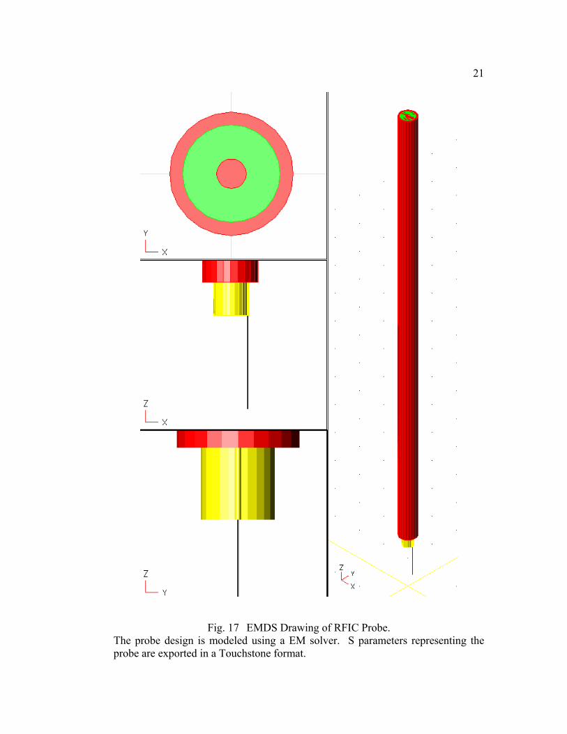
20 3.6 Probe Modeling
The preliminary calculations in the last section do not consider mutual
inductive effects or fringe capacitance of the capacitive coupler. Neither does it
consider the parasitic skin effect resistance of the tungsten needle. The probe is
drawn in Agilent Electromagnetic Design System (EMDS) and simulated over a
40 GHz range. As with a network analyzer the simulator exports S parameters in a
Touchstone format. The Touchstone file representing the modeled RFIC probe is
imported into ADS. Simulations can be performed using the file as if it is a sub-
circuit.
21
Fig. 17 EMDS Drawing of RFIC Probe. The probe design is modeled using a EM solver. S parameters representing the probe are exported in a Touchstone format.
22
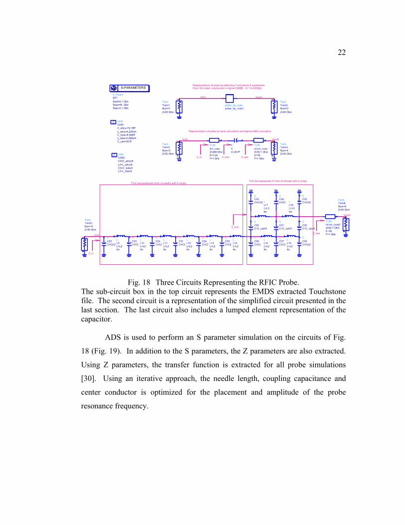
Fig. 18 Three Circuits Representing the RFIC Probe.
The sub-circuit box in the top circuit represents the EMDS extracted Touchstone file. The second circuit is a representation of the simplified circuit presented in the last section. The last circuit also includes a lumped element representation of the capacitor.
ADS is used to perform an S parameter simulation on the circuits of Fig.
18 (Fig. 19). In addition to the S parameters, the Z parameters are also extracted.
Using Z parameters, the transfer function is extracted for all probe simulations
[30]. Using an iterative approach, the needle length, coupling capacitance and
center conductor is optimized for the placement and amplitude of the probe
resonance frequency.
Vin3
Vin2
This box represents 2mm of needle with 6 lumps
Vout3
Z_last
Z_in
Representation of probe by hand calculation and Agilent ADS simulation.
Representation of probe by extracting Touchstone S parametersFrom 3D model constructed in Agilent EMDS (0.1 to 50GHz)
Vin1 Vout1
Vout2
Z_in Z_mid Z_last
This box represents 0.7mm of whisker with 2 lumps
Z_mid
VARVAR1
C_cplr=30 fFL_tube=0.588nHC_tube=9.268fFL_whis=4.225nH
C_whis=19.19fF
EqnVar
C
CC=30 fF
TermTerm6
Z=50 OhmNum=6
TermTerm5
Z=50 OhmNum=5
VARVAR2
L3=L_tube/2C3=C_tube/2L2=L_whis/8
C2=C_whis/8
EqnVar
S_ParamSP1
Step=0.1 GHzStop=40. GHzStart=0.1 GHz
S-PARAMETERS
TLINmicro_coax2
F=1 GHzE=36Z=50.1 Ohm
probe_tip_coaxprobe_tip_coax1
21
TermTerm3
Z=50 OhmNum=3
TermTerm4
Z=50 OhmNum=4
TermTerm2
Z=50 Ohm
Num=2
TermTerm1
Z=50 Ohm
Num=1
TLIN
Air_coax
F=1 GHzE=3.24Z=469 Ohm
TLIN
micro_coax
F=1 GHzE=36Z=50.1 Ohm
C
C26C=C2
C
C30C=C_cplr/4
CC33C=C3/2
CC35C=C3/2
CC34C=C3
C
C31C=C_cplr/2
C
C20C=C2/2
LL9
R=L=L2
LL10
R=L=L2
C
C21C=C2
LL11
R=L=L2
C
C22C=C2
LL12
R=L=L2
C
C23C=C2
C
C24C=C2
LL13
R=L=L2
C
C25C=C2
LL14
R=L=L2
C
C27C=C2
LL15
R=L=L2
LL16
R=L=L2
C
C28C=C2/2
C
C32C=C_cplr/4
LL18
R=
L=L3
LL17
R=
L=L3

23
Fig. 19 Comparison of the Transfer Function.
The comparison represents all models presented in Fig. 18. To minimize reflections below 10GHz, terminal 1 impedance is matched to the needle impedance on all probes.
3.7 RF Connector
The upper frequency limit of a RF connector is dependent on several
aspects [31]. High mechanical precision is required for a smooth transition from
connector to the cable. This lowers voltage reflections at high frequencies caused
by discontinuities. A medium with a low dielectric constant will cause lower
dispersion. Ideally the connector will have air as the dielectric medium. Lastly,
connector size is inversely proportional to its frequency response
A 2.92 mm connector is selected as the frequency response of this
connector is in excess of 40GHz [32]. This is the same connector type used by the
RF probes that will be used to characterize the RFIC probe. Additionally, 2.92mm
connectors are thread compatible with less expensive SubMiniature version A
(SMA) jacks for lower frequency applications.
Eqndelta_z1=Z(1,1)*Z(2,2)-Z(1,2)*Z(2,1)
EqnH1s1=Z(2,1)*PortZ(2)/(Z(1,1)*PortZ(2)+delta_z1)
1E9 1E101E8 4E10
-40
-20
0
-60
10
freq, Hz
dB
(H1
s1)
dB
(H1
s2)
dB
(H1
s3)
H1s1 H1s2 H1s3

24
Fig. 20 Completed Probe Assembly.
Shaft length: 30 mm (1 ¼ “) Needle length: 2 mm (1/16”) Needle diameter 16 microns (~1 mil)

25
4 RFIC PROBE CHARACTERIZATION
4.1 Introduction
Fig. 21 shows a square wave input signal and the RFIC probes
representation of that signal. Note the delay in signal propagation and the
differentiating action caused by the capacitive coupling. Also apparent is
reflections caused by impedance mismatch the circuit under test and the RFIC
probe. Clearly, further analysis will need to be done to recover the original square
wave.
Fig. 21 RFIC Probe Input and Output Signals.
4.2 S parameter Analysis
Using two 50 Ohm GSG Cascade Microwave probes, a 50 Ohm GSG
coupler on a Cascade test substrate a 40GHz vector network analyzer (VNA) is
calibrated (Appendix C). The microwave probe connected to port 2 is replaced
with the RFIC probe (Fig. 22).
An assumption is made that the second GSG microwave probe has a
negligible effect on the VNA calibration. Six frequency sweeps are made from
0.1GHz to 40GHz in 50MHz steps (Fig. 23). The results are averaged and S
parameters are saved in a Touchstone format.
0.2 0.4 0.6 0.8 1.0 1.2 1.40.0 1.6
-0.4
-0.2
0.0
0.2
0.4
-0.6
0.6
time, nsec
Vin
, V
Vou
t*10
Vin Vout*10

26
Fig. 22 VNA Setup for Probe Characterization.
The RFIC probe is analyzed from 0.1GHz to 40GHz and its S parameters are saved in a Touchstone file for later analysis with ADS.
Fig. 23 Analyzing the RFIC Probe on a Probe Station.
The probe on the left is a 50 Ohm Cascade GSG RF probe. It lands on a Cascade test substrate and the probe on the right is RFIC probe.
HP 8722CNetwork Analyzer
50 Ohm GSG CouplerOn Calibration Substrate
S1P_Eqnprobe2
P_ACPORT2
Z=50 OhmNum=2
P_ACPORT1
Z=50 OhmNum=1
S1P_EqnMicrowave_Probe

27 4.3 Transfer Function
A transfer function is defined as the output of a device vs. frequency
divided by the device input vs. frequency. Ideally, a probe would have a flat
transfer function. If the probe does not have a flat transfer function, the transfer
function itself can be used to mathematically flatten the probe response.
Two transfer function varieties are defined depending on what is to be
achieved. H1(s) (15) will allow Vin (The probe input) to be viewed given the
probe output Vout (Fig. 24). However, probing sensitive internal nodes on ICs
will adversely load the circuit. Using H1(s), (15) the signal at Vin is viewed. This
signal includes loading effects the probe has on the circuit.. Using H2(s), (16) the
signal at Vs is viewed. This is an advantage, as the node loading of the probe is
accounted for in the transfer function. By adding the output impedance of the
DUT to the probe transfer function, whatever loading the probe has on the circuit
will be de-embedded. Vin is viewed as if the probe is not loading that node.
Transfer function 1 ( )1( )( )
Vout sH sVin s
=
(15)
Transfer function 2 ( )2( )( )
Vout sH sVs s
= (16)
Fig. 24 Transfer Function Example.
Vin Vout
Vs P_nToneTerm1
Z=50 OhmNum=1
21
Ref TermTerm2
Z=50 OhmNum=2

28
The S parameters are converted to Z parameters then H1(s) is extracted
using (17) and (18) [30]. In the second case, we want to include the source
impedance in the transfer function (Fig. 24). Dividing the probe frequency
domain output signal by the frequency domain source signal reveals the transfer
function, H2(s) using S parameters (19) [33].
Delta Z (1,1) * (2, 2) (1, 2) * (2,1)Z Z Z Z ZΔ = − (17)
Transfer function 1 (2,1) *
1( )(1,1) *
L
L
Z ZH s
Z Z Z=
+ Δ (18)
Transfer function 2 (2,1)2( )2
SH s = (19)
Fig. 25 compares the transfer function of the 3D electromagnetic
simulation of the RFIC probe and manufactured probe 2. Fig. 27 compares the
transfer functions of manufactured probe 2. H1(s) relates Vout back to Vin and
H2(s) relates Vout back to Vs.
With identical terminations at both terminals, a enhanced comparison of
transfer functions would be to add 6dB to H2(s) (Fig. 27). High frequency
response is greater on H1(s). The RFIC probe will load a node with a capacitance.
With a high impedance node, this will create a low pass filter. H2(s) having a
lower high-frequency response will recreate the loaded signal at that node.
Chapter 5 will explore this further.

29
Fig. 25 H1(s) Transfer Functions of EMDS and Actual RFIC Probes.
The input impedance is set at 50 Ohms. Note low frequency ripples caused by impedance mismatch between the source and the needle.
Fig. 26 Comparisons Between H1(s) and H2(s) Response.
The amplitude difference between the transfer functions relates the amplitude between the source voltage, Vs and probe input voltage, Vin.
Eqn H1s_Probe2=Z(2,1)*PortZ(2)/(Z(1,1)*PortZ(2)+delta_z)
Eqn delta_z=Z(1,1)*Z(2,2)-Z(1,2)*Z(2,1)
Eqn H1s_EMDS=Z(4,3)*PortZ(4)/(Z(3,3)*PortZ(4)+delta_EMDS)
Eqn delta_EMDS=Z(3,3)*Z(4,4)-Z(3,4)*Z(4,3)
1E9 1E101E8 4E10
-50
-40
-30
-20
-10
-60
0
freq, Hz
dB(H
1s_E
MD
S)
dB(H
1s_
Pro
be2)
Eqn H2s_Probe2=S(2,1)/2
Eqn delta_z=Z(1,1)*Z(2,2)-Z(1,2)*Z(2,1)
Eqn H1s_Probe2=Z(2,1)*PortZ(2)/(Z(1,1)*PortZ(2)+delta_z)
1E9 1E101E8 4E10
-50
-40
-30
-20
-10
-60
0
freq, Hz
dB(H
1s_P
robe
2)dB
(H2s
_Pro
be2)
H1s EMDS H1s Probe2
H1s Probe2 H2s Probe2

30
Fig. 27 Shifted H1(s) and H2(s) Comparison.
In addition to the amplitude difference, H1(s) has a greater high frequency response.
1E9 1E101E8 4E10
-50
-40
-30
-20
-10
-60
0
freq, Hz
dB(H
1s_P
robe
2)dB
(H2s
_Pro
be2)
+6
H1s H2s+6dB

31
5 HIGH FREQUENCY TEST CIRCUITS
5.1 Introduction
To test the RFIC probe, several test circuits are designed [34]. These
circuits are designed to have a high frequency signal at a sensitive high impedance
node. Two oscillators are designed using a 0.18um CMOS BSIM3 model. A
Colpitts and a cross coupled oscillator are designed and modeled at 5.8GHz, which
is the middle of the 5.7GHz band [35]. Both oscillators are designed for a loop
gain of 2 using 0.8mA of current [34].
5.2 Colpitts Oscillator
A sensitive low power Colpitts oscillator is designed. The target frequency
of oscillation is 5.8GHz. Letting L=1nH and assuming a MOSFET parasitic
capacitance of 200fF, the equivalent series capacitance of C1 and C2 (Fig. 5) is
determined to be 0.583pF by (20). With a target N of 6, C1 and C2 is determined
to be 0.7pF and 3.5pF respectably by (21).
Fig. 28 5.8GHz Colpitts Oscillator. The oscillator is shown with probe and load resister. The load resistor is used to determine node resistance v1 and Vout using a voltage divider equation.
Using R1 as a resistor divider:The output resistance of node v1 is 3500 OhmsThe output resistance of node Vout is 950 Ohms
Vout Probe_out
V1 V1
Vout
RR1
MOSFET_NMOSMOSFET3
MOSFET_NMOSMOSFET2
TranTran2
StopTime=30.0 nsecStartTime=20 nsec
TRANSIENT
S_ParamSP1
Span=0.8 GHzCenter=5.7 GHz
S-PARAMETERSHarmonicBalanceHB1
FM_Noise=yesOrder[1]=12Freq[1]=5.7 GHz
HARMONIC BALANCE
S2PSNP3File="probe2A.s2p"
21
RefTermTerm2
Z=50 OhmNum=2
MOSFET_NMOSMOSFET1 I_DC
SRC1Idc=0.8 mA t
CC1C=0.7 pF
CC2C=3.5 pF
V_DCSRC2Vdc=3.0 V
V_DCSRC7Vdc=1.0 V
VARVAR1W1=50um
EqnVar
OscPortoscport1
ItStepSRC6
Rise=0.1 nsecDelay=0.1 nsecI_High=0 mAI_Low=-10 mA
LL1
R=0.4625L=1.03 nH
TermTerm1
Z=500 kOhmNum=1

32
Frequency 1
2f
LCequivπ= (20)
Transformer ratio 1 21
C CNC+
= (21)
Series Q _ LSeries QRω
= (22)
Series Parallel 2(1 )Rp Rs Q= + (23)
Impedance Matching 2
RpRsN
= (24)
Loop Gain 2
2
*_ *
1 *
Rpgm NLoop Gain NRpgm N
=+
(25)
Series Q of the inductor with 0.46 Ohms of parasitic resistance is
determined to be 79.2 by (22). A series parallel transformation determines
Rp=2900 by (23). To use the gain calculation of a source follower, Rp must be
moved to the source. This is done using the transformer formula by (24). Loop
gain is given by the voltage gain of a source follower multiplied by N. By
substituting the representation of Rs (24) into the source follower equation gives
(25). By extracting gm from ADS, The loop gain is set at 2 with a width of 50um.
5.3 Cross coupled oscillator
A sensitive low power cross-coupled oscillator is designed (Fig. 29). With
a width of 50um and a current of 0.8mA, Cdb is extracted as 0.500pF. With a
target frequency of 5.8GHz, L is determined to be 1.5nH using (26). Series Q of
the inductor with 5.7 Ohms of parasitic resistance is determined to be 9.57 by (27).
A series parallel transformation determines Rp=556 by (28). This gives a parallel
tank circuit on the drain of M1 consisting of L1, Cdb and Rp of 556. Transistor
M2 also has an equivalent tank. For a loop gain of 2, the resistance looking down
into M1, M2 should be one half Rp and is given by (29). With ADS, gm is
extracted and R is determined to be 267 Ohms using an iterative process.

33
For both Colpitts and cross-coupled oscillators, the node impedance is
determined by adding an external resistor at V1 and noting the voltage drop across
the respective node. This is repeated for Vout. Using the voltage divider equation
V1 is solved by (30). Solving for R2 gives the node impedance by (31).
Frequency 12
fLCπ
= (26)
Series Q _ LSeries QRω
= (27)
Series to Parallel 2(1 )Rp Rs Q= + (28)
Node Impedance 2Rgm
= (29)
Voltage Divider 111 2
RV VR R
=+
(30)
Divider Rearranged * 12 11
V RR RV
= − (31)

34
Fig. 29 5.8GHz Cross Coupled Oscillator. The oscillator is shown with probe and resistor to determine node resistance. Parasitic drain capacitance is used as the tank capacitance.
Probe_outVoutVoutV1
Using R1 as a resistor divider:The output resistance of node V1 is 340 OhmsThe output resistance of node Vout is 340 Ohms
TermTerm2
Z=50 OhmNum=2
S2PSNP3File="probe2A.s2p"
21
Ref
HarmonicBalanceHB1
FM_Noise=yesNLNoiseDec=2Freq[1]=5.8 GHz
HARMONIC BALANCE
TranTran2
StopTime=30.0 nsecStartTime=20 nsec
TRANSIENT
S_ParamSP1
Span=1 GHzCenter=5.8 GHz
S-PARAMETERS
RR1R=340 Ohm
LL1
R=5.7L=1.58 nH
LL2
R=5.7L=1.58 nH
MOSFET_NMOSMOSFET1
Width=50 umLength=0.36 um
I_DCSRC4Idc=0.8 mA
V_DCSRC3Vdc=1.5 V
VARVAR1W1=50um
EqnVar
OscPortoscport1
TermTerm1
Z=100 kOhmNum=1
ItStepJump_start
Rise=1 nsecDelay=2.0 nsecI_High=0 mAI_Low=-2 mA
MM9_PMOSMOSFET4
Width=50Length=0.36 umModel=PMOS_18
MM9_PMOSMOSFET3
Width=50 umLength=0.36 umModel=PMOS_18
MOSFET_NMOSMOSFET2
Width=50 umLength=0.36 um

35 5.4 22nm Inverter
Square waves are inherently more complex than sine waves because they
are represented as the sum of an infinite number of sine waves in the frequency
domain. Therefore the probe algorithm should be tested using a square wave. A
sensitive low current 22nm inverter is designed based on a BSIM4 CMOS model.
The input is a 10GHz signal with 20ps rise and fall times. The width of the PMOS
and NMOS transistors are selected to be the same strength. Vout is the loaded
output of the first inverter. As for the Colpitts and cross-coupled oscillators, the
node impedance is determined by adding an external resistor at Vout and noting
the voltage drop across the node. Using the voltage divider equation, Vout is
solved by (30). Solving for R2 gives the node impedance by (31). Vout node
impedance is verified by (32). Vout_not is checked during probing to ensure the
second inverter is functional.
Vout impedance (32)
Fig. 30 Inverter Modeled From 22nm CMOS Process. Vout is probed while Vout_not is checked to ensure the signal propagates to the second inverter.
Vout Probe_outVin
Vdd
Vout Vout Vout_not
VARohm130
P_w id=5.2 umN_w id=1.49 um
EqnVar
S2PSNP3File="probe2A.s2p"
21
Ref
TranTran2
StopTime=10.0 nsecStartTime=0 nsec
TRANSIENT
Vf_PulseSRC2
Fall=20 psecRise=20 psecWidth=30 psecFreq=10 GHzVpeak=1.2 V
BSIM4_NMOSm3
Width=N_w idLength=22nmModel=22nm_nmos
BSIM4_NMOSm2
Width=N_w idLength=22nmModel=22nm_nmos
BSIM4_PMOSm4
Width=P_w idLength=22nmModel=22nm_pmos
BSIM4_PMOSm1
Width=P_w idLength=22nmModel=22nm_pmos
V_DCSRC1Vdc=1.2 V
RR3R=50 Ohm

36 5.5 Summary
The circuits in this section are designed with sensitive nodes. In the
Colpitts oscillator, V1 has a high impedance. In the cross coupled oscillator, loop
gain is selected at 2, a minimum design value. The 22nm inverter uses the shortest
channel MOSFET model currently available [36]. Table 2 displays the
impedances of the nodes that will be probed.
Table 2 Node Impedances of Test Circuits
Impedance of Node (Ω)
Node Colpitts
Oscillator Cross Coupled
Oscillator 22nm
Inverter V1 3500 340
Vout 950 340 130

37
6 MEASUREMENTS AND SIGNAL RECOVERY
6.1 Introduction
In this chapter, the internal nodes will be probed on the Colpitts and Cross-
Coupled oscillators [34]. The 22nm inverter will also be probed. The
manufactured RFIC probe is used to measure a 200ps rise time step. Using the
derived transfer function and Fourier transforms, the input signal will be recreated.
6.2 Test Circuit Signal Recovery
When H(s) was derived, the source impedance was matched to the DUT
output impedance. All collected signals are sampled in time. The sampled time
domain probe output signal is represented as y(n). Next a fast Fourier transform
(FFT) on the sampled time domain probe signal is performed (33), bringing it into
the frequency domain Y(k). X(k) represents the output signal in the frequency
domain (34) [37]. The time domain signal x(n) can be recovered using an inverse
fast Fourier transform (IFFT) (35).
Frequency Domain Conversion (33)
Frequency Domain Input Signal (34)
Time Domain Conversion (35)
Recall Fig. 24 from chapter 4.3. Depending on whether the source or
probe input is to be viewed depends on which transfer function is selected. Using
H1(s) allows viewing at the RFIC probe input. By selecting H2(s), the voltage
source is viewed. H2(s) will enable viewing the input as if the probe does not load
the node.
( ) ( ( ))Y k FFT y n=( )( )( )
Y kX kH k
=
( ) ( ( ))x n IFFT X k=

38 6.3 Colpitts Oscillator
Fig. 31 through Table 3 represents probing the Colpitts oscillator. H1(s) is
used to recreate Vout. Using the built in ADS functions; H1(s) is calculated from
the derived Z parameters. The FFT is represented as fs and the IFFT is
represented as ts (Fig. 31). H2(s) cannot predict the frequency shift and other
adverse affects that putting a load on an oscillator so it is not used. Both probed
and un-probed oscillators are compared for amplitude and apparent phase shift
caused by a frequency shift (Fig. 32). Fig. 33 demonstrates circuit failure by
loading a sensitive high impedance node too much. The input impedance of the
probe will change the frequency of the oscillator tank circuit. Table 3 shows the
frequency and power of the fundamental oscillation frequency to the 12 harmonic
using a harmonic balance analysis in ADS. The probe shifted the oscillation
frequency by 0.2%.
Fig. 31 Colpitts Oscillator Output.
Using H1(s) the output signal is faithfully recreated.
Vout recovered Vout

39
Fig. 32 Probed and Un-probed Circuits are Compared.
The probe loads the Colpitts oscillator output and causes a slight frequency change from the un-probed oscillator.
Fig. 33 Colpitts V1 Failure.
Probing the sensitive v1 node causes oscillator failure.
29.05 29.10 29.1529.00 29.20
-450
-400
-350
-500
-300
time, nsec
Un
pro
be
d_
Vo
ut,
mV
Vo
ut,
mV
22 24 26 2820 30
-2
0
2
-4
4
time, nsec
v1, m
VUnprobed Vout Vout

40
Table 3 Colpitts Oscillator Spectral Analysis
Both probed and un-probed oscillators are compared to the 12th harmonic. Harmonic Probed_Colpitts Unprobed_Colpitts Index Freq. (GHz) Spectrum Freq. (GHz) Spectrum 0 0.00 2.0 0.00 2.0 1 5.78 ‐10.1 5.79 ‐10.4 2 11.57 ‐40.7 11.58 ‐41.4 3 17.35 ‐58.0 17.37 ‐58.6 4 23.14 ‐65.5 23.16 ‐66.4 5 28.92 ‐74.3 28.95 ‐75.2 6 34.71 ‐79.0 34.75 ‐79.9 7 40.49 ‐83.6 40.54 ‐84.6 8 46.28 ‐90.0 46.33 ‐91.0 9 52.06 ‐89.9 52.12 ‐91.1 10 57.85 ‐102.7 57.91 ‐103.1 11 63.63 ‐95.7 63.70 ‐97.1 12 69.42 ‐114.1 69.49 ‐114.3
6.4 Cross Coupled Oscillator
Fig. 34 through Table 4 represent probing the Cross Coupled oscillator.
H1(s) is used to recreate Vout. Using the built in ADS functions, H1(s) is
calculated from the derived Z parameters. The FFT is represented as fs and the
IFFT is represented as ts (Fig. 34). H2(s) cannot predict the frequency shift and
other adverse affects that putting a load on an oscillator so it is not used. Both
probed and un-probed oscillators are compared for amplitude and apparent phase
shift caused by a frequency shift (Fig. 35). With a symmetric oscillator design as
is the cross coupled, node v1 will give a response similar to Vout. Node V1 plots
are not shown. The input impedance of the probe will change the frequency of the
oscillator tank circuit. Table 4 shows the frequency and power of the fundamental
oscillation frequency to the 12 harmonic using a harmonic balance analysis in
ADS. The probe shifted the oscillation frequency by 2.4%.

41
Fig. 34 Cross Coupled Oscillator Output.
Using H1(s) the output signal is faithfully recreated.
Fig. 35 Probed and Un-probed Circuits are Compared.
The probe loads the Colpitts oscillator output and causes a slight frequency change from the un-probed oscillator.
29.75 29.80 29.8529.70 29.90
1
2
3
0
4
time, nsec
Unp
robe
d_V
out,
VV
out,
V
Vout recovered Vout
Unprobed Vout Vout

42
Table 4 Cross Coupled Oscillator Spectral Analysis
Both probed and un-probed oscillators are compared to the 12th harmonic. Harmonic Probed_Cross‐Coupled Unprobed_Cross‐Coupled Index Freq. (GHz) Spectrum Freq. (GHz) Spectrum 0 0.00 12.7 0.00 12.8 1 5.67 13.4 5.81 14.1 2 11.34 ‐2.8 11.61 2.4 3 17.01 ‐10.4 17.42 ‐14.6 4 22.67 ‐27.3 23.22 ‐27.9 5 28.34 ‐24.5 29.03 ‐23.0 6 34.01 ‐27.1 34.83 ‐27.7 7 39.68 ‐39.0 40.64 ‐32.7 8 45.35 ‐30.9 46.44 ‐31.9 9 51.02 ‐43.6 52.25 ‐45.4 10 56.69 ‐43.3 58.05 ‐38.3 11 62.36 ‐57.5 63.86 ‐54.5 12 68.02 ‐53.6 69.66 ‐46.0
6.5 22nm Inverter
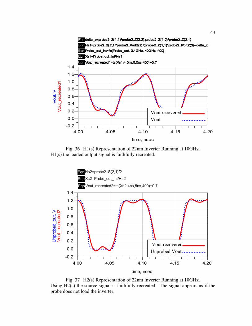
Fig. 36 through Fig. 38 represent probing a 22nm inverter running at
10GHz. Typically CMOS circuits are not forgiving to capacitive loads. Fig. 36
demonstrates using H1(s) to recreate Vout. Using the built in ADS functions,
H1(s) is calculated from the derived Z parameters. The FFT is represented as fs
and the IFFT is represented as ts. Fig. 37 demonstrates using H2(s) to derive Vout
without the probe loading. ADS calculates H2(s) directly from S(2,1). Fig. 38
checks the next inverter stage to ensure that the signal is propagating through to
that stage.
43
Fig. 36 H1(s) Representation of 22nm Inverter Running at 10GHz.
H1(s) the loaded output signal is faithfully recreated.
Fig. 37 H2(s) Representation of 22nm Inverter Running at 10GHz.
Using H2(s) the source signal is faithfully recreated. The signal appears as if the probe does not load the inverter.
4.05 4.10 4.154.00 4.20
0.0
0.2
0.4
0.6
0.8
1.0
1.2
-0.2
1.4
time, nsec
Vout_
recr
eate
d1
Vout, V
Eqn Hs2=probe2..S(2,1)/2
Eqn Xs2=Probe_out_int/Hs2
EqnVout_recreated2=ts(Xs2,4ns,5ns,400)+0.7
4.05 4.10 4.154.00 4.20
0.0
0.2
0.4
0.6
0.8
1.0
1.2
-0.2
1.4
time, nsec
Vou
t_re
crea
ted2
Unp
robe
d_ou
t, V
Vout recovered Vout
Vout recovered Unprobed Vout

44
Fig. 38 Output of the Second Inverter.
The output of the next stage is illustrated for both a probed and un-probed inverter.
6.6 Measured Pulse Generator Signal
In the last sections, the extracted parameters from a manufactured probe
are used on a simulated circuit. In this section, the manufactured probe is used on
a real circuit.
A step waveform from a 200ps rise time pulse generator is terminated into
50 Ohms. The probe output of a high speed pulse generator is sampled with a high
speed oscilloscope (Fig. 39). The pulse generator signal is also sampled and
displayed using a microwave probe along with the recovered input signal from the
RFIC probe (Fig. 40). As in the simulations, the RFIC probe transfer function is
determined and the step output of the high speed pulse generator is recovered
using the Matlab FFT and IFFT functions.
4.05 4.10 4.154.00 4.20
0.0
0.2
0.4
0.6
0.8
1.0
1.2
-0.2
1.4
time, nsec
Vou
t_no
t, V
Unp
robe
d_ou
t_no
t, V
Vout Unprobed Vout

45
Fig. 39 Sampled Probe Output
The probe signal is displayed using a 50 G samples per second oscilloscope
Fig. 40 Pulse Generator Waveform and the Recovered Signal
A 200ps risetime signal is displayed on a 50G sample/second oscilloscope using a microwave probe. The recovered signal from the RFIC probe is calculated and displayed concurrently.
0 0.2 0.4 0.6 0.8 1 1.2 1.4 1.6 1.8 2
x 10-9
-0.02
0
0.02
0.04
0.06
0.08
0.1
0.12
Time ( s )
Out
put ( V )
Sampled Probe Output
0 0.1 0.2 0.3 0.4 0.5 0.6 0.7 0.8 0.9 1
x 10-9
-0.2
0
0.2
0.4
0.6
0.8
1
1.2
1.4Waveforms from 200ps Pulse Generator
Time (s)
Vol
ts (V)
Probe Input
Recovered Input

46
7 CONCLUSION
The RFIC probe presented in this work demonstrates that high impedance
circuits operating at high frequency can be successfully probed. The probe has
an ultra low 30fF input capacitance to minimize circuit loading. 30fF is the lowest
input capacitance of available high impedance probes. Knowing the impedance of
the DUT, both Vin (loaded) and Vs (unloaded) waveforms can be recovered by
selecting the appropriate transfer function, S1(s) or S2(s).
The probe has a slim streamline design enabling better circuit viewing in a
probe station. Mechanically, the probe is easy to manufacture. Depending on the
application required, loading impedance and resonance frequency can be adjusted
by altering construction dimensions.
Future work may include adding resistance to the probe needle. This will
lower the probe Q. Resonance and anti-resonance points will be softened, leading
to a more consistent loading impedance above 15GHz. Characterizing the RFIC
probe to 40GHz limits the probe frequency response. Characterizing the probe to
a higher frequency will extend its frequency response. Moving the software
component of the RFIC probe into a sampling oscilloscope will enable almost real
time viewing of the recovered signal.

47
BIBLIOGRAPHY
[1] B. D. Beste and S. Griffiths. (2002, Oct.) Bill & Stan's Tektronix Resource
Site. [Online]. http://www.reprise.com/host/tektronix/reference/voltage_probes.asp
[2] Z. Yang, L. Wojewoda, L. Smith, H. Ishida, and M. Shimizu, "Inductance of Bypass Capacitors," in DesignCon 2005, Santa Clara, 2005, pp. 1-52.
[3] Tektronix. (2009, Feb.) Tektronix Enabling Innovation. [Online]. http://www.tek.com/products/accessories/oscilloscope_probes/
[4] American Probe & Technologies, Inc. (2005, Jan.) American Probe & Technologies, Inc. Home of the finest probing accessories. [Online]. http://www.americanprobe.com/triaxial-ph.htm
[5] Cascade Microtech, Inc. (2009, Feb.) Cascade Microtech, Inc. [Online]. http://www.cmicro.com/products/engineering-probes/rf-microwave
[6] GGB Industries Inc. Picoprobe. [Online]. http://www.ggb.com/index.html [7] W. S. Coates, R. J. Bosnyak, and I. E. Sutherland, "Method and apparatus for
probing an integrated circuit through capacitive coupling," Capacitively-coupled test probe Patent 6600325, Jul. 29, 2003.
[8] D. T. Crook and e. al, "Capacitively-coupled test probe," U.S. Patent 5274336, Dec. 28, 1993.
[9] G. E. Bridges, " Non-contact probing of integrated circuits and packages," Microwave Symposium Digest, 2004 IEEE MTT-S International, pp. 1805-1808, Jun. 2004.
[10] M. Tech. (2008, Dec.) Applied Chemical and Morphological Analysis Laboratory. [Online]. http://mcff.mtu.edu/acmal/veecodim3000.htm
[11] G. Majidi-Ahy and D. M. Bloom, "Millimeter-wave active probe system," U.S. Patent 5003253, Mar. 3, 1989.
[12] W. D. Edwards, J. G. Smith, and H. A. Kemhadjian, "SOME INVESTIGATIONS INTO OPTICAL PROBE TESTING OF INTEGRATED CIRCUITS.," Radio and Electronic Engineer, vol. 46, no. 1, p. 35, 1976.
[13] Agilent Technologies Inc. (2009) Manuals: Oscilliscope probes and accessories.
[14] D. M. Lauterbach, "Oscilloscope active probe," Test & Measurement World, Aug. 2001.

48
BIBLIOGRAPHY (Continued) [15] R. J. Adler. (2007) North Star High Voltage. [Online].
http://www.highvoltageprobes.com/index.html [16] S. M. Goldwater. (2009, Mar.) High Voltage Probe Frequency Response.
[Online]. http://www.repairfaq.org/sam/hvprobe.htm#shvmhf [17] J. L. Saunders and A. R. Loudermilk, "Methods for making contact device for
making connection to an electronic circuit device and methods of using the same," USA Patent 6343369 B1, Jan. 29, 2002.
[18] G. E. Bridges, "Non-contact probing of integrated circuits and packages," in Microwave Symposium , Fort Worth, TX, 2004, pp. 1805-1808.
[19] F Ho, A. S. Hou, B. A. Nechay,D. M. Bloom,"Ultrafast voltage-contrast scanning probe microscopy," Nanotechnology, pp. 385-389, 1996.
[20] Z. Weng, T. Kaminski, G. E. Bridges, and D. J. Thomson, "Resolution enhancement in probing of high-speed integrated circuits using dynamic electrostatic force-gradient microscopy," Journal of Vacuum Science and Technology A, pp. 948-953, 2004.
[21] C. J. Falkingham, I. H. Edwards, and G. E. Bridges, "Non-contact internal-MMIC measurement using scanning force probing," in Proceedings of the 1999 IEEE MTT-S International Microwave Symposium, Boston, MA, 2000, pp. 1619-1622.
[22] W. Mertin, "Contactless probing of high-frequency electrical signals with scanning probe microscopy," in EEE MTT-S International Microwave Symposium Digest, Seattle, WA, 2002, pp. 1493-1496.
[23] K. R. Gleason and K. E. Jones, "High-frequency active probe having replaceable contact needles ," U.S. Patent 5045781, Sep. 3, 1991.
[24] T. J. Zamborelli, "Wide bandwidth passive probe ," U.S. Patent 5172051, Dec. 15, 1992.
[25] K. Yang, G. David, and S. W. J. F. Robertson, "High-resolution electro-optic mapping of near-field distributions in integrated microwave circuits," in Microwave Symposium, Baltimore, MD, 1998, pp. 949-952.
[26] D.-J. Lee and J. F. Whitaker, "An optical-fiber-scale electro-optic probe for minimally invasive high-frequency field sensing," Optics Express, vol. 16, no. 26, pp. 21587-21597, Dec. 2008.
[27] A. Weisshaar, ECE 699 class notes. Corvallis, Oregon, Dept of EECS, Oregon State University, Fall 2007.

49
BIBLIOGRAPHY (Continued) [28] L. Forbes, D. A. Miller, and M. E. Jacob, "Low capacitance electrical probe for
nanoscale devices and circuits," Open Nanoscience Journal, vol. 2, no. 1, pp. 39-43, Aug. 2008.
[29] Micro-Coax, UT-47-M17 Data Sheet. 2003, Cut-off frequency is 136GHz. [30] J. W. Nilsson and S. A. Riedel, Electric Circuits, 6th ed. Upper Saddle River,
New Jersey, USA: Prentice-Hall, 2000. [31] Micro-Coax. (2003) Micro-Coax. [Online]. http://www.micro-
coax.com/pages/technicalinfo/applications/26.asp [32] P-N Designs Inc. (2006, Apr.) Microwaves101.com. [Online].
http://www.microwaves101.com/encyclopedia/connectorsprecision.cfm#24mm[33] B. Frank. (2007, Sep.) Queen's University. [Online].
http://bmf.ece.queensu.ca/mediawiki/index.php/Network_Parameters [34] K. Mayaram, ECE 621 class notes. Corvallis, Oregon: Dept of EECS, Oregon
State University, Winter 2008. [35] T. N. Cokienias, "New rules for unlicensed digital transmission systems,"
Compliance Engineering, no. Spring, 2002. [36] Nanoscale Integration and Modeling (NIMO) Group,. (2007, Oct.) Predictive
Technology Model (PTM). [Online]. http://www.eas.asu.edu/~ptm/latest.html [37] S. Haykin and B. V. Veen, Signals and Systems Second Edition, B. Zobrist, Ed.
Hoboken, United States of America: John Wiley & Sons Inc., 2003. [38] M. E. Jacob, D. A. Miller, and L. Forbes, "Ultra low capacitance high
frequency IC probe," Proceedings of SPIE, the International Society for Optical Engineering, vol. 7042, pp. 7042031-7042039, Aug. 2008.
[39] M. E. Jacob, D. A. Miller, and L. Forbes, "Ultra low capacitance, high frequency RFIC probe," in 2008 IEEE Workshop on Microelectronics and Electron Devices (WMED), Boise, 2008, pp. 32-33.

50
APPENDICES

51
Appendix A – Coaxial Specifications
206 Jones Blvd. Pottstown, PA 19464 USA Phone: 610-495-0110 : 800-223-2629 www.micro-coax.com
UT-47-M17 (M17/151-00001)
Semi-Rigid Coaxial Cable
MECHANICAL CHARACTERISTICS
Outer Conductor Diameter, inch (mm) 0.047+/-0.001 (1.194+/-0.0254) Dielectric Diameter, inch (mm) 0.037 (0.94) Center Conductor Diameter, inch (mm) 0.0113+/-0.0005 (0.287+/-0.0127) Maximum Length, feet (meters) 20 (6.1) Minimum Inside Bend Radius, inch (mm) 0.125 (3.175) Weight, pounds/100 ft. (kg/100 meters) 0.45 (0.67)
ELECTRICAL CHARACTERISTICS
Impedance, ohms 50+/-2.5 Frequency Range GHz DC-20 Velocity of Propagation % 70 Capacitance, pF/ft. (pF/meter) 32.2 (105.6) Typical Insertion Loss, dB/ft. (dB/meter) and Average Power Handling, Watts CW at 20 degrees Celsius and Sea level
Frequency Insertion Loss Power 0.5 GHz 1.0 GHz 5.0 GHz 10.0 GHz 20.0 GHz
0.28 (0.92) 0.40 (1.31) 0.90 (2.95) 1.30 (4.27) 1.90 (6.23)
45 32 13 9 6.5
Corona Extinction Voltage, VRMS @ 60 Hz 1000 Voltage Withstand, VRMS @ 60 Hz 2000
ENVIRONMENTAL CHARACTERISTICS
Outer Conductor Integrity Temperature, Deg Celsius 175 Maximum Operating Temperature, Deg Celsius 100
MATERIALS
Outer Conductor Copper Dielectric PTFE Center Conductor SPCW
CUTAWAY

52
206 Jones Blvd. Pottstown, PA 19464 USA Phone: 610-495-0110 : 800-223-2629 www.micro-coax.com
Attenuation (Theoretical) at 20°C
Cutoff Frequency

53
Appendix B – Probe Design

54

55
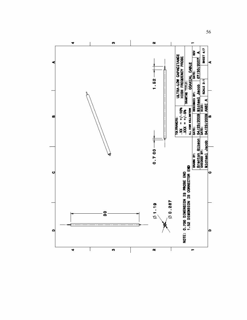
56

57

58

59

60
Appendix C – Test Substrate

61
Appendix D – HSpice, 2D Circuit Simulation
************************************************ * Whisker_coupler_together7.23.sp * Author: Drake Miller & Michael Jacob * Date: 7/16/07 * Revised 7.23.07 Michael Jacob * W element field solver for probe whisker attached to coupler ********************************************* ********************** *Constants ********************** .PARAM Whs_len = "2mm" .PARAM coup_len = "0.7mm" .PARAM CtoC_sep = "0.185mm" .PARAM whs_rad = "8um" .PARAM coax_inner_rad = "100um" .PARAM layer_pos = "2.5mm+CtoC_sep" .OPTION PROBE POST ********************** *2ps rise time pulse ********************** VIMPULSE 1 gnd PULSE 0v 1v 5p 2p 2p 50p *use for tran *i1 1 gnd AC 1 *use for AC ********************** *U Element simulates whisker *The 3mm Tungsten Whisker by radius 10um ********************** U1 w_in gnd w_in1 gnd air_coax l="whs_len" *Whisker length Rinput 1 w_in 300 *assume perfect input R_con w_in1 in1 0.01 *connect whisker to coupler ********************** *W Element ********************** W1 in1 in2 gnd out1 out2 gnd + FSmodel=whisker N=2 l="coup_len" *coupler overlap Rin1 1 in1 .0325 * least reflection at 325 ohms Rin2 in2 gnd 325Meg * least reflection at 325 ohms Rout2 out2 gnd 270 *assume termination to ideal coax *********************** *Materials FR4 at 1 GHz *********************** .MATERIAL diel_fr4 DIELECTRIC ER=4.3 LOSSTANGENT=0.015 .MATERIAL diel_epoxy DIELECTRIC ER=4 LOSSTANGENT=0.015

62 .MATERIAL copper METAL CONDUCTIVITY=59.61meg *********************** * Coax Shapes *********************** .SHAPE whisker CIRCLE radius="whs_rad" *whisker radius .SHAPE micro_coax CIRCLE radius = "coax_inner_rad" *coax inner conductor radius *********************** *Uses the default AIR *background *********************** .LAYERSTACK stack_1 LAYER=(PEC, 1um) + LAYER=(air,2.5mm) + LAYER=(diel_epoxy,1mm) *********************** *Option settings *********************** .FSOPTIONS opt1 PRINTDATA=YES ACCURACY=HIGH *********************** *Two different conductor shapes *Air coax *********************** .MODEL whisker W MODELTYPE=FieldSolver, + LAYERSTACK=stack_1, FSOPTIONS=opt1, + RLGCFILE=coupled.rlgc + CONDUCTOR=(SHAPE=whisker,ORIGIN= + (2.5mm, 5mm), MATERIAL=copper) + CONDUCTOR=(SHAPE=micro_coax, + ORIGIN=("layer_pos", 5mm), MATERIAL=copper) *layer_pos is specified C to C plus 2.5mm .MODEL air_coax u LEVEL=3 plev=2 elev=1 + RA="whs_rad" RB=2.5mm RHO=52.9n RHOB=17n KD=1 ************************ *Analysis, outputs and end ************************ .TRAN .1p 0.16n *use for tran *.tf v(out2) V(1) *use for tran *.AC Dec 1000 4GHz 40GHz *use for AC .PROBE v(out2) v(in1) V(1) V(w_in) i(Rin1) i(Rw) *probe V(w_in) whisker input impedance *.PRINT v(1) v(w_in) *use for AC .END

63 ************************************************ * Whisker_coupler_coax_filter_simple_PWL_rev1.sp * Author: Michael Jacob & Drake Miller * Date: 7/25/07 Revised 7.30.07 * 8.21.07 add resistance and capacitance to DUT * W element field solver for probe whisker attached to coupler, coax and filter * ********************************************* ********************** *Constants ********************** .PARAM Whs_len = "2mm" .PARAM coup_len = "0.7mm" .PARAM CtoC_sep = "0.368mm" .PARAM whs_rad = "8um" .PARAM coax_inner_rad = "0.3mm" .PARAM layer_pos = "2.5mm+CtoC_sep" ********************** *2ps rise time pulse ********************** *VIMPULSE 1 gnd PULSE 0v 1v 0p 25p 75p 511p *use for tran Vinpwl 1 gnd PWL (0ps, 0V) (20ps, 0V) (40ps, 1V) (60ps, 1V) (70ps, 2v) (80ps, 1V) (90ps, 2V) (100ps, 1V) (110ps, 2V) (120ps, 1V) (200ps, 1V) (300ps, 0.5v) (500ps, 0V) *i1 1 gnd AC 1 *use for AC Rinput 1 2 1000 *assume perfect input with 343 Ohms Cinput 2 gnd 50fF *assume 50fF parasitic cap R_con1 2 w_in 0.01 *connects probe to circuit pick this or *E1 w_in gnd 2 gnd 1 *isolates probe loading pick this ********************** *U Element simulates whisker *The 3mm Tungsten Whisker by radius 10um ********************** U1 w_in gnd w_in1 gnd air_coax l="whs_len" *Whisker length R_con w_in1 in1 0.01 *connect whisker to coupler (should be zero) ********************** *W Element ********************** W1 in1 in2 gnd out1 out2 gnd + FSmodel=whisker N=2 l="coup_len" *coupler overlap Rin1 in2 gnd 325Meg * Provides path for spice Rin2 out1 gnd 325Meg * Provides path for spice ********************** *U Element and termination ********************** U2 out2 gnd out3 gnd UT-47 l=30mm *micro coax

64 Rout2 out3 gnd 50 *assume termination to ideal coax ********************** *50GHz Low pass filter at end of coax ********************** R1 out3 out4 1000 C1 out4 gnd 20fF *********************** *Materials FR4 at 1Ghz *********************** .MATERIAL diel_fr4 DIELECTRIC ER=4.3 LOSSTANGENT=0.015 .MATERIAL diel_epoxy DIELECTRIC ER=4 LOSSTANGENT=0.015 .MATERIAL copper METAL CONDUCTIVITY=59.61meg *********************** * Coax Shapes *********************** .SHAPE whisker CIRCLE radius="whs_rad" *whisker radius .SHAPE micro_coax CIRCLE radius = "coax_inner_rad" *coax inner conductor radius *********************** *Uses the default AIR *background *********************** .LAYERSTACK stack_1 LAYER=(PEC, 1um) + LAYER=(air,2.5mm) + LAYER=(diel_epoxy,1mm) *********************** *Option settings *********************** .FSOPTIONS opt1 PRINTDATA=YES ACCURACY=HIGH *********************** *Two different conductor shapes *Air coax *********************** .MODEL whisker W MODELTYPE=FieldSolver, + LAYERSTACK=stack_1, FSOPTIONS=opt1, + RLGCFILE=coupled.rlgc + CONDUCTOR=(SHAPE=whisker,ORIGIN= + (2.5mm, 5mm), MATERIAL=copper) + CONDUCTOR=(SHAPE=micro_coax, + ORIGIN=("layer_pos", 5mm), MATERIAL=copper) *layer_pos is specified C to C plus 2.5mm *********************** *Model *UT-47-M17 Micro coax *********************** .MODEL UT-47 u LEVEL=3 plev=2 elev=1 wlump=30 maxl=300

65 + RA=144um RB=470um RD=597um RHO=17n RHOB=17n KD=2.1 .MODEL air_coax u LEVEL=3 plev=2 elev=1 + RA="whs_rad" RB=2.5mm RHO=52.9n RHOB=17n KD=1 ************************ *Analysis, outputs and end ************************ .TRAN 1p 1.023n *use for tran *.tf v(out2) V(1) *use for tran *.AC Dec 1000 4GHz 40GHz *use for AC *.PROBE v(out4) V(out3) v(in1) V(1) V(w_in) i(Rin1) i(Rw) *probe V(w_in) whisker input impedance .OPTION INGOLD=2 .OPTION PROBE POST .PROBE tran PAR('v(1)*1') PAR('v(out3)*1') PAR('v(out4)*1') *use for AC *prints in exponential format .PRINT PAR('v(1)*1') PAR('v(2)*1') PAR('v(out4)*1') *use for AC .END

66
Appendix E – Matlab, Probe Hand Calculations %Michael Jacob %5.23.08 %Probe hand calculations %lengths in meters or mm converted to meters close all, clear all, clc; %matlab housekeeping %% constants c = 3e8; %light speed m/s Eo = 8.85e-12; %permittivity of free space F/m Uo = pi*4e-7; %permeability of free space H/m ZL = 50; %termination impedance freq = 1e9; %1GHz for determining electrical length whis_len = 2.7e-3; %2.7mm whis_rad = 0.008e-3; %0.008mm whis_shld_rad = 20e-3; %20mm spacing = 0.37e-3 %whisker-tube spacing overlap = 0.7e-3 %whisker-tube overlap that creates the capacitor Er = 2.02; %dielectric constant of Teflon mc_wire_rad = 0.1435e-3;%radius of micro coax wire mc_shld_rad = 0.47e-3; %radius of shield mc_len = 30e-3; %length of micro coax tube_rad = 0.3e-3; %tube that surrounds coax wire %% Acquire the Impedance waveform in the test file generated by ADS % Using this style ignores the ADS header fid = fopen('C:\Documents\ADS\probe_hand_calc_prj\data\matlab_z.s1p', 'r'); [s_matrix] = textscan(fid, '%f %f %f', 300, 'headerlines', 5); fclose(fid); % create a ninety X 1 column array from the ninety X 3 array x = s_matrix1; % get the first column data (frequency) ads_Z = s_matrix2; % get the second column data (real) ads_angle = s_matrix3; % get the third column data (angle) f = x'; %rotate frequency matrix 90 degrees %% microcoax calculations mc_C = 2*pi*Eo*Er/log(mc_shld_rad/mc_wire_rad); %per unit length mc_L = Uo/(2*pi)*log(mc_shld_rad/mc_wire_rad); %per unit length mc_Zo = sqrt(mc_L/mc_C) %50 ohm coax vp = c/sqrt(Er); mc_Beta = 2*pi.*f./vp; mc_elec_len = 360*mc_len*freq/vp Z_last = mc_Zo.*(ZL+j.*mc_Zo.*tan(mc_Beta.*mc_len))./(mc_Zo + j.*ZL.*tan(mc_Beta.*mc_len)); %%capacitor calculation separation = spacing-tube_rad-whis_rad C = 2*pi*Eo/acosh(2*separation/(2*whis_rad))*overlap %whisker to plane approximation XC = 1./(j*2*pi*C.*f); %capacitive reactance Z_mid = XC+Z_last; %% air coax calculations whis_C = 2*pi*Eo/log(whis_shld_rad/whis_rad); %per unit length whis_L = Uo/(2*pi)*log(whis_shld_rad/whis_rad);%per unit length whis_Zo = sqrt(whis_L/whis_C)

67 whis_Beta = 2*pi.*f./c; whis_elec_len = 360*whis_len*freq/c Zin = whis_Zo.*(Z_mid+j.*whis_Zo.*tan(whis_Beta.*whis_len))./(whis_Zo + j.*Z_mid.*tan(whis_Beta.*whis_len)); %% approximate transfer function calculation Hs =(ZL./(ZL+Zin)); %% Plots subplot (2,1,1); % plot the impedance loglog (x/1e9,ads_Z, 'bo', 'MarkerSize',7); % ads calculation grid hold on; loglog (f/1e9, abs(Zin),'r','LineWidth',2); % matlab calculation hold off; title ('Probe Input Impedance vs Frequency'); %detail the plot xlabel ('Frequency (GHz)'); ylabel ('Impedance (Ohms)'); legend ('ADS','Matlab'); subplot (2,1,2); % plot the approx transfer function semilogx (f/1e9, 20*log10(abs(Hs)),'r','LineWidth',2); % matlab calculation grid hold off; title ('Probe Approx. Transfer Function vs Frequency'); %detail the plot xlabel ('Frequency (GHz)'); ylabel ('H(s) (dB)'); legend ('Matlab');

68
Appendix F – Matlab, HSpice to FFT %%%%%%%%%%%%%%%%%%%%%%%%%%%%%%%%%%%%%%%%%%%%%%%%%%%% %Author: Michael Jacob %Date: 8.14.07 %Revision: 8.21.07 8.22.07 Uses updated spice files that have %input resistance as part of the DUT. %This program loads HSpice simulation from a text file into the workspace. %A frequency domain transfer function is determined from a square wave %input and the resulting system output using both direct non filtered %output and 50GHz RC filter output %%%%%%%%%%%%%%%%%%%%%%%%%%%%%%%%%%%%%%%%%%%%%%%%%%% close all; %Matlab housekeeping clear all; clc; %%%%%%%%%%%%%%%%%%%%%%%%%%%%%%%%%%%%%%%%%%%%%%%%%%%% %Open HSpice .lis file, extract the data into a Matlab column matrix. %Reshape the column matrix into a 4 row matrix %and split into respective 1X matrices %%%%%%%%%%%%%%%%%%%%%%%%%%%%%%%%%%%%%%%%%%%%%%%%%%%% Fid = fopen('C:\Documents\Michael''s Classes\Probe\HSpice\whisker_coupler_coax_filter_simple_rev1.lis'); while 1 tline = fgetl(fid); %read file line by line if ~ischar(tline), break, end %go until EOF if tline ==('x') %Look for beginning of data tline = fgetl(fid); %ignore the 3 line data header tline = fgetl(fid); tline = fgetl(fid); %read string data into column matrix until it reaches non numeric SpiceData= fscanf(fid,'%g'); len= length (SpiceData); % the length of the column matrix SpiceData=reshape(SpiceData,[4 len/4]);%reshape into 4 row matrix end end fclose(fid); time = SpiceData(1,:); %time matrix 0 to 1023ps clk_input = SpiceData(2,:); %input signal input = SpiceData(3,:); %probe input signal output = SpiceData(4,:); %LP 50GHz filtered output %%%%%%%%%%%%%%%%%%%%%%%%%%%%%%%%%%%%%%%%%%%%% %figure 1 %plot HSpice pulse %plot simulated transistor output %plot probe output %%%%%%%%%%%%%%%%%%%%%%%%%%%%%%%%%%%%%%%%%%%%% plot (time,clk_input,'y','LineWidth',2); %HSpice pulse hold on plot (time,input) %Probe input plot (time,100*output,'g') %Probe output X 100

69 legend ('DUT input vs time', 'Probe input vs time', 'Probe output X100 vs time'); xlabel ('time (s)'),ylabel ('volts') hold off grid on; %%%%%%%%%%%%%%%%%%%%%%%%%%%%%%%%%%%%%%%%%%%%% %Change the input and output signals into the frequency domain and %deconvolve H(s) transfer function. Convert H(s) to h(t). Randomly %choose 1024 points %%%%%%%%%%%%%%%%%%%%%%%%%%%%%%%%%%%%%%%%%%%%% %Change to freq X = fft(input,1024); Y2 = fft(output,1024); H2 = Y2./X; %filtered H(s) %change transfer function back to time h2 = ifft(H2, 1024); %filtered h(t) %%%%%%%%%%%%%%%%%%%%%%%%%%%%%%%%%%%%%%%%%% %View the time domain transfer function from probe input to filtered output %%%%%%%%%%%%%%%%%%%%%%%%%%%%%%%%%%%%%%%%%% figure %2 %figure 2 plot (time,h2) %Impuse function legend ('time domain transfer function vs time'); axis tight grid on; %%%%%%%%%%%%%%%%%%%%%%%%%%%%%%%%%%%%%%%%%%%% %division of Y(s)/H(s)=X(s) which is the frequency representation of the %original signal. An inverse Fourier transform derives x(t) (the original %signal) %%%%%%%%%%%%%%%%%%%%%%%%%%%%%%%%%%%%%%%%%%%% X_reconst2=Y2./H2; x_reconst2= ifft(X_reconst2,1024); figure %3 %figure 3 plot (time, x_reconst2,'y','LineWidth',2); %reconstructed input hold on; plot(time,input,'b--') %input signal legend ('reconstructed input vs time by means of Fourier transforms','Probe input vs time'); xlabel ('time (s)'),ylabel ('volts') hold off; grid on %%%%%%%%%%%%%%%%%%%%%%%%%%%%%%%%%%%%%%%%%%%%%%%%%%%% %Now test with an filtered input arbitrary waveform %Open HSpice .lis file, extract the data into a Matlab column matrix. %Reshape the column matrix into a 4 row matrix %and split into respective 1X matrices %%%%%%%%%%%%%%%%%%%%%%%%%%%%%%%%%%%%%%%%%%%%%%%%%%%% fid=fopen('C:\Documents\Michael''s Classes\Probe\HSpice\whisker_coupler_coax_filter_simple_PWL_rev1.lis'); while 1 tline = fgetl(fid); %read file line by line if ~ischar(tline), break, end %go until EOF if tline ==('x') %Look for beginning of data tline = fgetl(fid); %ignore the 3 line data header tline = fgetl(fid); tline = fgetl(fid);

70 %read string data into column matrix until it reaches non numeric SpiceData_1= fscanf(fid,'%g'); len= length (SpiceData_1); % the length of the column matrix SpiceData_1=reshape(SpiceData_1,[4 len/4]); %reshape into 4 row matrix end end fclose(fid); %%%%%%%%%%%%%%%%%%%%%%%%%%%%%%%%%%%%%%%%%%% %plot HSpice pulse %plot simulated transistor output %plot probe output %%%%%%%%%%%%%%%%%%%%%%%%%%%%%%%%%%%%%%%%%%%%% figure %4 %figure 4 plot (time,SpiceData_1(2,:),'y','LineWidth',2); %Hspice PWL pulse hold on plot (time,(SpiceData_1(3,:))) %Probe input plot (time,(100*SpiceData_1(4,:)),'g') %Probe output X 100 legend ('DUT input vs time', 'Probe input vs time', 'Probe output X100 vs time'); xlabel ('time (s)'),ylabel ('volts') hold off grid on; Y4 = fft(SpiceData_1(4,:),1024); %filtered sample X_reconst4 = Y4./H2; x_reconst4 = ifft(X_reconst4,1024); figure %5 %figure 5 plot (time, x_reconst4,'y','LineWidth',2); %reconstructed input hold on; plot(time,SpiceData_1(3,:),'b--') %probe input legend ('reconstructed input vs time by means of Fourier transforms','Probe input vs time'); xlabel ('time (s)'),ylabel ('volts') grid on;