
controlling mesoporous layer 3 Improved stability of ... · Improved stability of perovskite solar...
7
Supporting Information for: Improved stability of perovskite solar cells in ambient air by controlling mesoporous layer Jun Yin, a,b Jing Cao, b Xu He, a Shangfu Yuan, b Shibo Sun, a Jing Li,* a,c Nanfeng Zheng,* b and Liwei Lin c a. Pen-Tung Sah Institute of Micro-Nano Science and Technology, Xiamen University, Xiamen, 361005, China. E-mail: [email protected]; Tel: +86-592-2181340. b. State Key Laboratory for Physical Chemistry of Solid Surfaces, Collaborative Innovation Center of Chemistry for Energy Materials, and Department of Chemistry, College of Chemistry and Chemical Engineering, Xiamen University, Xiamen 361005, China. E-mail: [email protected]; Fax: +86-592- 2183047. c. Department of Mechanical Engineering, University of California, Berkeley, CA 94720, United States. 1. Experimental details Solar cell fabrication: Fluorine doped tin oxide (FTO) glasses (NSG, 14 Ω) were ultrasonically cleaned by ethanol and acetone for 20 min sequentially, and then treated by O 2 plasma for 6 min. The compact TiO 2 (c-TiO 2 ) film was formed by spin-coating 0.15 M titanium diisopropoxide bis (acetylacetonate) (75 wt% in isopropanol, TCI) in n-butanol on the FTO substrates at 2500 rpm for 30 s, then dried at 125 °C for 10 min and annealed at 550 °C in air for 30 min. After that, the substrates were immersed in 40 mM TiCl 4 aqueous solution for 30 min at 70 °C and washed with distilled water, followed by annealing at 500 °C for 30 min in air. The m-TiO 2 layer was deposited by spin coating a commercial TiO 2 paste (Dyesol 18NRT) diluted in ethanol (1:5, weight ratio) at 5000 rpm for 30 s, and annealed at 500 °C for 30 min. To control the thickness of m-TiO 2 layer, different spin-coating times were introduced. The perovskite film was prepared using the widely used two-step method: PbI 2 solution (1 M) in N, N- dimethylformamide (DMF) was spin-cast on the m-TiO 2 layer followed by immersing in CH 3 NH 3 I solution and the subsequent thermal treatment. The hole-transporting material (HTM) layer was then deposited by spin coating a solution of spiro-MeOTAD (Lumtech) at 4000 rpm for 30 s. Finally, 80 nm-thick gold electrodes were deposited by electron beam Electronic Supplementary Material (ESI) for Journal of Materials Chemistry A. This journal is © The Royal Society of Chemistry 2015
Transcript of controlling mesoporous layer 3 Improved stability of ... · Improved stability of perovskite solar...

Supporting Information for:
Improved stability of perovskite solar cells in ambient air by controlling mesoporous layer
Jun Yin,a,b Jing Cao,b Xu He,a Shangfu Yuan,b Shibo Sun,a Jing Li,*a,c Nanfeng Zheng,*b and Liwei Linc
a. Pen-Tung Sah Institute of Micro-Nano Science and Technology, Xiamen University, Xiamen, 361005, China. E-mail: [email protected]; Tel: +86-592-2181340.
b. State Key Laboratory for Physical Chemistry of Solid Surfaces, Collaborative Innovation Center of Chemistry for Energy Materials, and Department of Chemistry, College of Chemistry and Chemical Engineering, Xiamen University, Xiamen 361005, China. E-mail: [email protected]; Fax: +86-592-2183047.
c. Department of Mechanical Engineering, University of California, Berkeley, CA 94720, United States.
1. Experimental details
Solar cell fabrication:
Fluorine doped tin oxide (FTO) glasses (NSG, 14 Ω) were ultrasonically cleaned by ethanol
and acetone for 20 min sequentially, and then treated by O2 plasma for 6 min. The compact
TiO2 (c-TiO2) film was formed by spin-coating 0.15 M titanium diisopropoxide bis
(acetylacetonate) (75 wt% in isopropanol, TCI) in n-butanol on the FTO substrates at 2500 rpm
for 30 s, then dried at 125 °C for 10 min and annealed at 550 °C in air for 30 min. After that,
the substrates were immersed in 40 mM TiCl4 aqueous solution for 30 min at 70 °C and washed
with distilled water, followed by annealing at 500 °C for 30 min in air. The m-TiO2 layer was
deposited by spin coating a commercial TiO2 paste (Dyesol 18NRT) diluted in ethanol (1:5,
weight ratio) at 5000 rpm for 30 s, and annealed at 500 °C for 30 min. To control the thickness
of m-TiO2 layer, different spin-coating times were introduced. The perovskite film was
prepared using the widely used two-step method: PbI2 solution (1 M) in N, N-
dimethylformamide (DMF) was spin-cast on the m-TiO2 layer followed by immersing in
CH3NH3I solution and the subsequent thermal treatment. The hole-transporting material
(HTM) layer was then deposited by spin coating a solution of spiro-MeOTAD (Lumtech) at
4000 rpm for 30 s. Finally, 80 nm-thick gold electrodes were deposited by electron beam
Electronic Supplementary Material (ESI) for Journal of Materials Chemistry A.This journal is © The Royal Society of Chemistry 2015
evaporation through a shadow mask. All of the devices were fabricated under ambient air with
humidity about 50% and then stored in dry air environment without sealing and maintaining
the humidity of ~15% before measurements.
Device characterization:
Absorption spectra of perovskite films were recorded using a Shimadzu UV 2550 UV-Visible
spectrophotometer. The morphologies were investigated using a field-emission scanning
electron microscopy (SEM) (Hitachi S-4800), and the crystallinity of the perovskite films was
characterized by an X-ray diffraction (XRD) (Rigaku Ultima IV) with Cu Ka radiation in a 2θ
range of 10 - 35°. Photovoltaic J-V measurements were performed under AM 1.5G illumination
at the intensity of 100 mW cm-2 using a 300 W Xenon solar simulator (Newport) equipped with
a Keithley 2420 source meter. The incident photon to electron conversion efficiency (IPCE)
was measured using a power source (Newport, 300 W xenon lamp, 66920) with a
monochromator (Newport, Cornerstone 260) and an optical power meter (Newport, 2936-R).
Electrochemical impedance spectra (EIS) measurements were carried out on CHI660 under 1
sun illumination with different DC bias voltage from 0.4 to 1.0 V. A small AC voltage
perturbation of 10 mV was applied during the measurement at frequency ranging from 1 Hz to
1 MHz. The spectra were fitted using Z-View software. The time-resolved PL (TRPL) spectra
were recorded on a fluorescence spectrometer (FLS980, Edinburgh Photonics) excited by
picosecond pulsed diode lasers (375 nm).

2. Cross-section morphology of the perovskite films
Figure S1. Cross-section SEM images of the perovskite films on different thicknesses of m-
TiO2 layer by changing spin-coating times: (a) 1 time, (b) 2 times, (c) 3 times and (d) 4 times.
Scale bar represents 500 nm.

3. Histogram of PCE for samples with 160-nm thick m-TiO2 layer
Figure S2. Histogram of solar cell efficiency of 18 samples (a) without and (b) with
optimization. In this work, the most efficient cells were realized on the devices configured by
m-TiO2 with the thickness of ~160 nm and achieved the PCE of 11.09% (10.43% in average),
as shown in (a). With optimized perovskite layer, 13.76% PCE (12.41% in average) can be
obtained as shown in (b). (c) J-V curves measured by reverse- and forward-scan for a typical
device configured with 160 nm-thick m-TiO2 layer. The scan rate was 150 mV/s.
4. IPCE spectra for the devices with different thickness of m-TiO2 layer
Figure S3 m-TiO2-thickness dependence of the IPCE response for the perovskite solar cells.
The integrated photocurrent density Jsc from IPCE spectra was also shown in the figure with a
value of 16.74, 17.19, 17.12, and 16.51 mA cm-2 for the device with 160, 240, 330 and 415
nm-thick m-TiO2 layer, respectively. The integrated Jsc from IPCE matched well with the J-V
measurement results, and also undergo a slight increase and then decrease trend.

5. Electrochemical impedance spectra (EIS) measurement
Figure. S4 (a) EIS of the cells with different thickness of m-TiO2 layer under AM 1.5G
illumination (100 mW cm-2) and 1.0 V bias. (b) Recombination resistance (Rrec) estimated from
the EIS measurements as a function of the applied voltage (0.4 - 1.0 V) to the devices. The EIS
spectra is fitted using transmission line model1 and Rrec is extracted and plotted as a function
of the applied voltage bias. Equivalent circuit is shown in inset of (a). R1 and C1 represent the
hole transport resistance and capacitance through the hole transport material (HTM) layer.

6. Long-term PCE stability of the devices
Figure S5. (a) and (b) show the J-V curves for the same device with 240-nm-m-TiO2 layer that
measured immediately and after 100 days of ageing, respectively. The PV parameters measured
by reverse- and forward-scan are summarized in inset. The devices were stored in air ambient
with controlled humidity of ~15% and without sealing. A maximum of 9.15% PCE still can be
obtained on this structure even after 100 days (~ 2400 hours).
7. Time-resolved PL (TRPL) measurement
Figure S6. Time-resolved photoluminescence (TRPL) spectra of the perovskite films
configured with (a) 160 nm- and (b) 240 nm- thick m-TiO2 layer before and after aging (7 days)
in air under controlled humidity (~ 15%).
In order to further evaluate the charges transportation process for the cells with different
thickness of m-TiO2 layer after aging, time-resolved photoluminescence (TRPL) were carried
out to determine the carriers’ lifetime in perovskite film as shown in Figure S6. The curves can
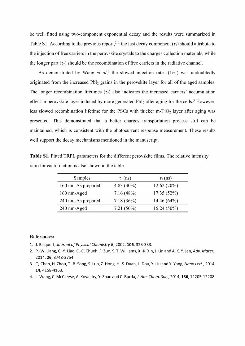
be well fitted using two-component exponential decay and the results were summarized in
Table S1. According to the previous report,2, 3 the fast decay component (τ1) should attribute to
the injection of free carriers in the perovskite crystals to the charges collection materials, while
the longer part (τ2) should be the recombination of free carriers in the radiative channel.
As demonstrated by Wang et al,4 the slowed injection rates (1/τ1) was undoubtedly
originated from the increased PbI2 grains in the perovskite layer for all of the aged samples.
The longer recombination lifetimes (τ2) also indicates the increased carriers’ accumulation
effect in perovskite layer induced by more generated PbI2 after aging for the cells.3 However,
less slowed recombination lifetime for the PSCs with thicker m-TiO2 layer after aging was
presented. This demonstrated that a better charges transportation process still can be
maintained, which is consistent with the photocurrent response measurement. These results
well support the decay mechanisms mentioned in the manuscript.
Table S1. Fitted TRPL parameters for the different perovskite films. The relative intensity
ratio for each fraction is also shown in the table.
Samples τ1 (ns) τ2 (ns)160 nm-As prepared 4.83 (30%) 12.62 (70%)160 nm-Aged 7.16 (48%) 17.35 (52%)240 nm-As prepared 7.18 (36%) 14.46 (64%)240 nm-Aged 7.21 (50%) 15.24 (50%)
References:1. J. Bisquert, Journal of Physical Chemistry B, 2002, 106, 325-333.2. P.-W. Liang, C.-Y. Liao, C.-C. Chueh, F. Zuo, S. T. Williams, X.-K. Xin, J. Lin and A. K. Y. Jen, Adv. Mater.,
2014, 26, 3748-3754.3. Q. Chen, H. Zhou, T.-B. Song, S. Luo, Z. Hong, H.-S. Duan, L. Dou, Y. Liu and Y. Yang, Nano Lett., 2014,
14, 4158-4163.4. L. Wang, C. McCleese, A. Kovalsky, Y. Zhao and C. Burda, J. Am. Chem. Soc., 2014, 136, 12205-12208.