Considerations for Measuring Loop Gain in Power Supplies PPT
45
Power Supply Design Seminar Reproduced from 2018Texas Instruments Power Supply Design Seminar SEM2300 TI Literature Number: SLUP387 © 2018 Texas Instruments Incorporated Power Supplyt Design Seminar resources are available at: www.ti.com/psds Considerations for Measuring Loop Gain in Power Supplies
Transcript of Considerations for Measuring Loop Gain in Power Supplies PPT

Power Supply Design Seminar
Reproduced from 2018Texas Instruments Power Supply Design Seminar SEM2300
TI Literature Number: SLUP387© 2018 Texas Instruments Incorporated
Power Supplyt Design Seminar resources are available at: www.ti.com/psds
Considerations for Measuring Loop Gain in Power Supplies

Texas Instruments – 2018 Power Supply Design Seminar
Considerations for Measuring Loop Gain in Power Supplies Manjing Xie
6-1

Texas Instruments – 2018 Power Supply Design Seminar
Outline • Introduction – loop gain overview • Empirical loop gain measurement methods • Test setup and test examples
– Frequency analyzer setup – Preparing converter for loop gain measurement – Connecting equipment to circuit under test
• Summary
6-2

Texas Instruments – 2018 Power Supply Design Seminar
Introduction – Loop Gain Overview • What is loop gain? • Why do we measure loop gain?
6-3

Texas Instruments – 2018 Power Supply Design Seminar
Introduction – What Is Loop Gain? Loop gain: product of all gains around feedback loop
G(s)
H(s)
- VOUT
T(s)
Simple Feedback System DC/DC Converter Control System
6-4
T(s)=G(s)⋅H(s)
VIN +
Power Stage
FB
VOUT
VREF COMP RBOTTOM
RTOP
Error Amplifier
T(s)
PWM Comparator
+ -
+-
VIN
VOUT
COUT
L

Texas Instruments – 2018 Power Supply Design Seminar 6-5
Why Do We Measure Loop Gain? 1) Loop gain is good indicator of stability
Load Step, 2 A/div
VOUT (AC), 10 mV/div
fC = 22.4 kHz Phase Margin = 15 º
Frequency (Hz)
Loop Gain Transient Response
Output Oscillates at about 20 kHz

Texas Instruments – 2018 Power Supply Design Seminar 6-6
Why Do We Measure Loop Gain? 2) Loop gain results guide us to improve load transient response
Given the loop is stable, higher loop bandwidth improves transient response [1]
IOUT, 2 A/div
tP = 1
4 ⋅ fC
VP = ΔI
8 ⋅ fC ⋅COUTVOUT, 100 mV/div
Texas Instruments – 2018 Power Supply Design Seminar
Loop Gain Measurement Method
6-7

Texas Instruments – 2018 Power Supply Design Seminar
Power Stage
FB
VOUT
VREF COMP RBOTTOM
RTOP
Error Amplifier
T(s)
PWM Comparator
+ -
+-
VIN
VOUT
COUT
L
Loop Gain Measured in Open-Loop Setup
• Difficult to maintain correct DC operating point due to high DC gain
• Easy to saturate circuits by injecting too much AC disturbance
It is not practical to measure loop gain in open-loop setup
× ×
B
A
! 6-8
VINJ ~

Texas Instruments – 2018 Power Supply Design Seminar
Power Stage
FB
VOUT
VREF COMP RBOTTOM
RTOP
Error Amplifier
T(s)
PWM Comparator
+ -
+-
VIN
VOUT
COUT
L
Equivalent Circuit of Feedback System
Thevenin's Theorem
×
×
B
A
Looking Backward
Look
ing
Forw
ard
6-9
+ ‒
A
Looking Forward
VA ~ Z1
+ ‒
GND
VCVS
Looking Backward
B
VY ~
Z2
!VY (s)= - M(s)⋅ !VA(s)
T(s)= M(s)⋅
Z1Z1 + Z2
+ ‒


Texas Instruments – 2018 Power Supply Design Seminar
Test Setup
• Frequency analyzer setup • Selecting the correct injection isolator • Preparing converter for loop gain measurement • Minimizing error
6-11
Texas Instruments – 2018 Power Supply Design Seminar
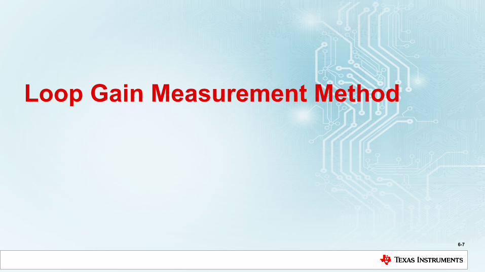
Typical Loop Gain Measurement Setup
• Setting up equipment – Frequency analyzer – Source injection isolator
• Setting up power supply
– Identify voltage injection point
– Connect equipment to circuit
6-12

Texas Instruments – 2018 Power Supply Design Seminar
• Provides AC voltage source:
• Measures response:
• Calculates loop gain:
Frequency Analyzer’s Functions
Voltage Source ROUT = 50 Ω
Receiver A
Receiver B
6-13
!VSRC
!VA and !VB
T(s)= −!VB!VA
Image reproduced with permission from AP Instruments, Inc.
Texas Instruments – 2018 Power Supply Design Seminar
-60 -50 -40 -30 -20 -10
0 10 20 30
0.1 1 10 100 1000
Mag
nitu
de (d
B)
Frequency (kHz)
Gain from
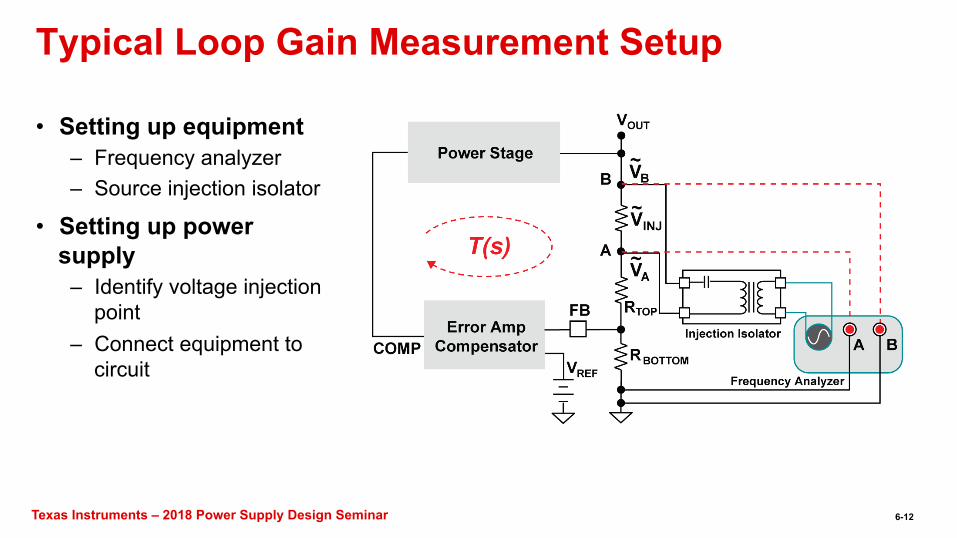
Injecting Sufficient AC Voltage AP300 Specification: Measurable Signal Range 5 µV to 1.77 V
System closed-loop response:
6-14
!VINJ to !VA and !VB
!VB(s) = T(s)1+T(s)
!VINJ (s) !VA(s) = -11+T(s)
!VINJ (s)
!VA(s)!VINJ (s)
!VB(s)!VINJ (s)
!VA
!VB• Both and should beof sufficient amplitude for loop gain measurement
• At f = 100 Hz, to have
• At f = 300 kHz, to have
V!A >5 µV, V!INJ >5 mV
V!B >5 µV, V!INJ >50 µV

Texas Instruments – 2018 Power Supply Design Seminar
Excessive Voltage Injection Leads to Saturation
What could happen if voltage injection is excessive? • Duty-cycle saturation
• Error amplifier saturation
• False triggering of over-current protection
• False triggering of over-voltage protection
• LDO driver and pass device saturation
6-15
Power Stage
FB
VOUT
VREF COMP RBOTTOM
RTOP
Error Amplifier
T(s)
PWM Comparator
+ -
+-
GPS(s)
VOUT
COUT
L
VINJ ~
d(s)
B
A

Texas Instruments – 2018 Power Supply Design Seminar
-‐180
-‐135
-‐90
-‐45
0
45
90
135
180
0.1 1 10 100 1000
VSRC = 2mV, Constant
VSRC ProgrammedVSRC Programmed— VSRC Programmed — VSRC Programmed
-‐60
-‐45
-‐30
-‐15
0
15
30
45
60
0.1 1 10 100 1000
VSRC = 2mV, Constant
VSRC = 10mV, ConstantVSRC = 10mV, Constant– VSRC = 10 mV, Constant
Programmable VSRC
Mag
nitu
de (d
B)
Phas
e (d
egre
e)
Frequency (kHz)
Error Due to Low
Frequency (kHz)
Loop Gain Measurement with Different VSRC
Programmable VSRC
High VSRC at Low Frequencies
VSRC is the voltage source of the frequency analyzer
6-16
VA ~
– VSRC = 2 mV, Constant – VSRC = 2 mV, Constant – VSRC = 10 mV, Constant
(Image reproduced with permission from Ridley Engineering Inc.)

Texas Instruments – 2018 Power Supply Design Seminar
Servo Control VSRC
Mag
nitu
de (d
B)
Phas
e (d
egre
e)
Frequency (kHz) Frequency (kHz)
Loop Gain Measurement with Different VSRC
6-17
-‐180
-‐135
-‐90
-‐45
0
45
90
135
180
0.1 1 10 100 1000
VSRC= 100mV, constant
-‐60
-‐45
-‐30
-‐15
0
15
30
45
60
0.1 1 10 100 1000
VSRC= 100mV, constant VSRC = 100 mV, Constant VSRC = 100 mV, Constant
VSRC= 50mV, constant VSRC= 50mV, constant— VSRC = 50 mV, Constant — VSRC = 50 mV, Constant
VSRC ProgrammedVSRC Programmed— VSRC Programmed — VSRC Programmed
Monitor Receiver signals Minimum VSRC
VSRC Servo: When CH1 or CH2 signal < threshold, VSRC increases per step size
Generated by Venable Instruments' Stability Analysis Software and reproduced here with permission from Venable Instruments.

Texas Instruments – 2018 Power Supply Design Seminar
Frequency Analyzer– IF Bandwidth (Integration Time)
Narrow intermediate frequency (IF) BW: + Less susceptible to random noise ‒ Longer sweeping time
6-18
BW = 100 Hz
BW = 10 Hz
BW = 100 Hz
BW = 10 Hz
Frequency (kHz) Generated by Venable Instruments' Stability Analysis Software and reproduced here with permission from Venable Instruments.
Image reproduced with permission from Ridley Engineering Inc.

Texas Instruments – 2018 Power Supply Design Seminar
Using Injection Isolator with Correct Frequency Range
Injection Isolator BODE BOXTM: Injection Isolator + Pre-Connected Signal Receiver
Active BODE BOXTM
6-19
Image used with permission from Venable Instruments.
Image used with permission from Venable Instruments.
Image reproduced with permission from Ridley Engineering Inc.

Texas Instruments – 2018 Power Supply Design Seminar
• Identify correct voltage injection point• Connect equipment to circuit under test
Setting Up Circuit for Loop Gain Measurement
6-20

Texas Instruments – 2018 Power Supply Design Seminar
Maintaining DC Static Operating Point Insert small resistor (10 Ω to 100 Ω ) between point A and B to maintain ~ same static operating point
Source ROUT = 50 Ω 6-21
VSRC is the AC source of frequency analyzer
~ Image used with permission from Venable Instruments.
Image reproduced with permission from AP Instruments, Inc.

Texas Instruments – 2018 Power Supply Design Seminar
Measuring Loop-Gain for VMC TPS40425, Dual-Phase Buck Converter
Measured crossover frequency and phase margin match simulation well!
6-22


Texas Instruments – 2018 Power Supply Design Seminar
1 A LED Lighting Driver
Measuring Loop Gain for LED Driver
6-24
T(s) VY ~
+ ‒
!VY (s)= - M(s)⋅ !VA(s)
Z1
0.7 Ω
GND
VINJ ~
VA ~ VB
~
Measured Loop Gain

Texas Instruments – 2018 Power Supply Design Seminar
Multiple Feedback Paths
• Bandwidth of T(s) canpredict transientperformance
• Loop gain withfeedback path 2closed:
• Bandwidth of TM(s)might not tell howtransient responseperforms
6-25
IOUT, 2 A/div
VOUT, 100 mV/div
T(s) = H1(s)+H2(s)
ZOUT(CLOSED)(s) = ZOUT(OPEN)(s)
1+ H1(s)+H2(s)
TM (s) = H1(s)
1+H2(s)
ZOUT(CLOSED)(s) = ZOUT(OPEN)(s)
1+T(s)VP = ΔI
8 ⋅ fC ⋅COUT

Texas Instruments – 2018 Power Supply Design Seminar
Multiple Feedback Paths – Isolated Converter
9.4 A to 12.6 A Step
VOUT, 200 mV/div
Time: 50 µsec/div
Measured loop gain correlates well with transient response
The correct injection point includes all feedback paths
VOUT
fC = 15 kHz
0.1 1 10 100
Mag
nitu
de (d
B)
Phas
e (d
egre
e)
Frequency (kHz) VIN = 54 V, IOUT = 12.6 A VIN = 54 V, IOUT = 8 A
40
30
20
10
0
-10
-20
-30
-40 180
150
120
90
60
30
0
-30
-60
tP ≅ 1
4 ⋅ fC= 16.7 µsec
tP = 16 µsec
6-26

Texas Instruments – 2018 Power Supply Design Seminar
-‐50
-‐40
-‐30
-‐20
-‐10
0
10
20
30
40
50
0 1 10 100 1,000
Magnitude
(dB)
Frequency (kHz)
Setup 1 Setup 2
-‐90
-‐60
-‐30
0
30
60
90
120
150
180
0.1 1 10 100 1000
Phase (degree)
Frequency (kHz)
Setup 1 Setup 2
52 kHz
Multiple Feedback Paths – D-CAP™ Control
14 kHz
Mag
nitu
de (d
B)
Phas
e(de
gree
)
0.1 1 10 100 1000
Frequency(kHz)
50 kHz
Measured Loop Gain
Measurement matches transient response
6-27
1
2
Measurement matches calculation
Mag
nitu
de (d
B)
Frequency(kHz)
tP = 5.2 µsec fc ≈ 48 kHz
Calculated Loop Gain

20

Texas Instruments – 2018 Power Supply Design Seminar
–12
0
0
180
Phas
e (d
egre
e)
Mag
nitu
de (d
B)
–40
0
60
Measuring Loop Gain for PFC Converter Challenges of measuring loop gain for power factor correction converter • Low control bandwidth
• High output voltage
• Use DC input
Isolator of correct frequency range
High-voltage frequency analyzer
Oscilloscope for gain and phase measurement
OR + [5]
VIN = 150 V
Loop Gain of PMP5242, PFC SEPIC
1 10 100 Frequency (Hz)
VIN = 300 V
High Voltage Setting
6-29
AC
Vol
tage
(20
mV/
div)
Voltage Node B
Voltage Node A
Phase Shift
20 µs/div Image used with permission from Ridley Engineering Inc.
Generated by Venable Instruments' Stability Analysis Software and reproduced here with permission from Venable Instruments.

Texas Instruments – 2018 Power Supply Design Seminar
Connecting Equipment to Converter
• How connection wires affect loop gain measurement • Where to connect reference leads of two receivers
6-30

Texas Instruments – 2018 Power Supply Design Seminar
-‐30
-‐20
-‐10
0
10
20
30
40
50
Magnitude
(dB)
Single pair, 6 inches
-‐60
-‐30
0
30
60
90
120
150
180
1.00E+02 1.00E+03 1.00E+04 1.00E+05 1.00E+06
Phase (degree)
Frequency (Hz)
Single pair, 6 inches
Connection Wires Affect Loop Gain Measurement TPS53355 VIN = 12 V VOUT = 1.2 V FSW = 400 kHz Why does the gain increase at high frequency
Measured Loop Gain Bode plot measured with single-pair 6-inch long wires
Bode plot with 0.5-inch short wires to connect receivers and adaptor to converter under test
6-31
while the phase drops rapidly?
Single Pair, 0.5 inch
Single Pair, 6 Inches
Single Pair, 0.5 Inches
Single Pair, 0.5 inch
Single Pair, 6 Inches
Single Pair, 0.5 Inches
0.1 1 10 100 1000

Texas Instruments – 2018 Power Supply Design Seminar
How Connection Wires Affect Loop Gain Measurement Receivers and adaptor share one pair of wires
Measured loop gain:
At high frequencies:
Recommendation: • Use wires as short as possible • Use separate wires for measurement
and voltage injection
Receivers and adaptor use separate wires
6-32
TM (s) = - !VB(s)!VA(s)
= T(s)+(1+T(s))⋅
ZL(s)ZINJ (s)
1+(1+T(s))⋅ZL(s)
ZINJ (s)
TM (+j∞ ) ≈
ZL(+ j∞ )ZINJ (+ j∞ )+ ZL(+ j∞ )
T(s) T(s)

Texas Instruments – 2018 Power Supply Design Seminar
-‐30
-‐20
-‐10
0
10
20
30
40
50
Magnitude
(dB)
-‐60
-‐30
0
30
60
90
120
150
180
1.00E+02 1.00E+03 1.00E+04 1.00E+05 1.00E+06
Phase (degree)
Frequency (Hz)
Two Pairs, 6 inches
Single Pair, 0.5 inch
Two Pairs, 6 Inches Single Pair, 0.5 Inches
Bench Verifications Measurement results are similar
Mag
nitu
de (d
B)
Phas
e (d
egre
e)
0.1 1 10 100 1000 Frequency (kHz)
Two Pairs of Wires
One Pair of Wires
Receiver B
Receiver B
Voltage Injection
6-33

Texas Instruments – 2018 Power Supply Design Seminar
Considerations for Bode Box™ Receivers are pre-connected to output of injection isolator
Receivers are forced to sense voltage drops across connection cable
6-34
T(s)
-‐60
-‐30
0
30
60
90
120
150
180
0 1 10 100 1,000
Phase (degree)
Frequency (kHz)
Bode Box, 3 feetTwo Pairs, 6 inches
-‐30
-‐20
-‐10
0
10
20
30
40
50
Magnitude
(dB)
Bode Box, 3 feetTwo Pairs, 6 inchesBode Box, 3 Feet Two Pairs, 6 Inches
Bode Box, 3 Feet Two Pairs, 6 Inches

Texas Instruments – 2018 Power Supply Design Seminar
Which Is the Correct Reference Point?
Voltage Injection Point A and B
Receiver A, B Coaxial Cables
Reference Leads
Reference Clip
• For single-ended system, use controller signal ground for reference
• For converter with fully differential remote sensing, use remote negative sense for reference
6-35
Image reproduced with permission from Ridley Engineering Inc. and AP Instruments, Inc.

Texas Instruments – 2018 Power Supply Design Seminar
LM4041-N Shunt-Regulator
Block Diagram
• GND is the reference point • VINJ is injected between VOUT
and RTOP
• VOUT is the reference point • VINJ is injected between
GND and RBOTTOM
"
V REF
Ref
ers
to V
OU
T
! 6-36
Typical Circuit 12 V
10 kΩ
10 kΩ
10 kΩ LM4041-ADJ
VOUT
220 nF

Texas Instruments – 2018 Power Supply Design Seminar
Check Stability Over All Conditions
• Over input voltage range
• Over output current range
• Over temperature range
• Over output voltage range
-‐60
-‐50
-‐40
-‐30
-‐20
-‐10
0
10
20
30
40
Magnitude
(dB)
Vin = 54V, IO = 12.6A
Vin = 54V, IO = 8A
Vin = 54V, IO = 3A
Vin = 54V, IO = 1.25A
Vin = 54V, IO = 0A
-‐60
-‐30
0
30
60
90
120
150
180
0.1 1 10 100
Phase (degree)
Frequency (Hz) Thousands
Vin = 54V, IO = 12.6A
Vin = 54V, IO = 8A
Vin = 54V, IO = 3A
Vin = 54V, IO = 1.25A
Vin = 54V, IO = 0A
Compensation network should be designed so that system is stable over all conditions:
6-37
— VIN = 54 V, IOUT = 12.6 A — VIN = 54 V, IOUT = 8 A — VIN = 54 V, IOUT = 3 A --- VIN = 54 V, IOUT = 1.25 A --- VIN = 54 V, IOUT = 0 A
— VIN = 54 V, IOUT = 12.6 A — VIN = 54 V, IOUT = 8 A — VIN = 54 V, IOUT = 3 A --- VIN = 54 V, IOUT = 1.25 A --- VIN = 54 V, IOUT = 0 A

Texas Instruments – 2018 Power Supply Design Seminar
Summary • Prepare circuit for test
– Identify correct voltage injection point • Impedance looking backward should be as small as possible • Injection point should include all output feedback paths
– Identify correct reference point
• Setup frequency analyzer with correct voltage source amplitude • Select right injection isolator
• Maintain same DC and AC static operating point
• Receivers should not include voltage drops on connection wires • Check stability over all conditions
6-38

Texas Instruments – 2018 Power Supply Design Seminar
References • [1] Bob Sheehan, “How to determine bandwidth from the transient-
response measurement,” Power Tips Blog. • [2]John Betten, “Calculating capacitance for load transients”, Power
Tips, May 17th, 2015. • [3] John Betten,“Control Loop Considerations for an LED Driver,”
EETimes, August 17, 2007. • [4] Datasheet of LM4041-N. • [5] Application Note AN1889, “How to measure the loop transfer
function of power supplies.”
6-39

Texas Instruments – 2018 Power Supply Design Seminar
Appendix
6-40

Texas Instruments – 2018 Power Supply Design Seminar
Derivation of Closed-Loop Responses
When Z2 = 0 Ω, T(s) = M(s)
6-41
VCVS
T(s)
B A
VY ~
+ ‒
!VY (s)= - M(s)⋅ !VA(s)
Z1
Z2
VCOM
VINJ ~
VA ~ VB
~
!VB(s) = -T(s)⋅ !VA(s)!VINJ (s) = !VB(s) - !VA(s)= - T(s)+1( ) ⋅ !VA(s)
⇒ !VA(s) = - 1T(s)+1
⋅ !VINJ (s)
⇒ !VB(s) = T(s)T(s)+1
⋅ !VINJ (s)
VA(s)
-
+


SLUP387
TI Worldwide Technical Support
Important Notice: The products and services of Texas Instruments Incorporated and its subsidiaries described herein are sold subject to TI’s standard terms and conditions of sale. Customers are advised to obtain the most current and complete information about TI products and services before placing orders. TI assumes no liability for applications assistance, customer’s applications or product designs, software performance, or infringement of patents. The publication of information regarding any other company’s products or services does not constitute TI’s approval, warranty or endorsement thereof.
The platform bar and E2E are trademarks of Texas Instruments.All other trademarks are the property of their respective owners.
TI SupportThank you for your business. Find the answer to your support need or get in touch with our support center at
www.ti.com/support
China: http://www.ti.com.cn/guidedsupport/cn/docs/supporthome.tsp
Japan: http://www.tij.co.jp/guidedsupport/jp/docs/supporthome.tsp
Technical support forumsSearch through millions of technical questions and answers at TI’s E2E™ Community (engineer-to-engineer) at
e2e.ti.com
China: http://www.deyisupport.com/
Japan: http://e2e.ti.com/group/jp/
B011617
TI TrainingFrom technology fundamentals to advanced implementation, we offer on-demand and live training to help bring your next-generation designs to life. Get started now at
training.ti.com
China: http://www.ti.com.cn/general/cn/docs/gencontent.tsp?contentId=71968
Japan: https://training.ti.com/jp

IMPORTANT NOTICE FOR TI DESIGN INFORMATION AND RESOURCES
Texas Instruments Incorporated (‘TI”) technical, application or other design advice, services or information, including, but not limited to,reference designs and materials relating to evaluation modules, (collectively, “TI Resources”) are intended to assist designers who aredeveloping applications that incorporate TI products; by downloading, accessing or using any particular TI Resource in any way, you(individually or, if you are acting on behalf of a company, your company) agree to use it solely for this purpose and subject to the terms ofthis Notice.TI’s provision of TI Resources does not expand or otherwise alter TI’s applicable published warranties or warranty disclaimers for TIproducts, and no additional obligations or liabilities arise from TI providing such TI Resources. TI reserves the right to make corrections,enhancements, improvements and other changes to its TI Resources.You understand and agree that you remain responsible for using your independent analysis, evaluation and judgment in designing yourapplications and that you have full and exclusive responsibility to assure the safety of your applications and compliance of your applications(and of all TI products used in or for your applications) with all applicable regulations, laws and other applicable requirements. Yourepresent that, with respect to your applications, you have all the necessary expertise to create and implement safeguards that (1)anticipate dangerous consequences of failures, (2) monitor failures and their consequences, and (3) lessen the likelihood of failures thatmight cause harm and take appropriate actions. You agree that prior to using or distributing any applications that include TI products, youwill thoroughly test such applications and the functionality of such TI products as used in such applications. TI has not conducted anytesting other than that specifically described in the published documentation for a particular TI Resource.You are authorized to use, copy and modify any individual TI Resource only in connection with the development of applications that includethe TI product(s) identified in such TI Resource. NO OTHER LICENSE, EXPRESS OR IMPLIED, BY ESTOPPEL OR OTHERWISE TOANY OTHER TI INTELLECTUAL PROPERTY RIGHT, AND NO LICENSE TO ANY TECHNOLOGY OR INTELLECTUAL PROPERTYRIGHT OF TI OR ANY THIRD PARTY IS GRANTED HEREIN, including but not limited to any patent right, copyright, mask work right, orother intellectual property right relating to any combination, machine, or process in which TI products or services are used. Informationregarding or referencing third-party products or services does not constitute a license to use such products or services, or a warranty orendorsement thereof. Use of TI Resources may require a license from a third party under the patents or other intellectual property of thethird party, or a license from TI under the patents or other intellectual property of TI.TI RESOURCES ARE PROVIDED “AS IS” AND WITH ALL FAULTS. TI DISCLAIMS ALL OTHER WARRANTIES ORREPRESENTATIONS, EXPRESS OR IMPLIED, REGARDING TI RESOURCES OR USE THEREOF, INCLUDING BUT NOT LIMITED TOACCURACY OR COMPLETENESS, TITLE, ANY EPIDEMIC FAILURE WARRANTY AND ANY IMPLIED WARRANTIES OFMERCHANTABILITY, FITNESS FOR A PARTICULAR PURPOSE, AND NON-INFRINGEMENT OF ANY THIRD PARTY INTELLECTUALPROPERTY RIGHTS.TI SHALL NOT BE LIABLE FOR AND SHALL NOT DEFEND OR INDEMNIFY YOU AGAINST ANY CLAIM, INCLUDING BUT NOTLIMITED TO ANY INFRINGEMENT CLAIM THAT RELATES TO OR IS BASED ON ANY COMBINATION OF PRODUCTS EVEN IFDESCRIBED IN TI RESOURCES OR OTHERWISE. IN NO EVENT SHALL TI BE LIABLE FOR ANY ACTUAL, DIRECT, SPECIAL,COLLATERAL, INDIRECT, PUNITIVE, INCIDENTAL, CONSEQUENTIAL OR EXEMPLARY DAMAGES IN CONNECTION WITH ORARISING OUT OF TI RESOURCES OR USE THEREOF, AND REGARDLESS OF WHETHER TI HAS BEEN ADVISED OF THEPOSSIBILITY OF SUCH DAMAGES.You agree to fully indemnify TI and its representatives against any damages, costs, losses, and/or liabilities arising out of your non-compliance with the terms and provisions of this Notice.This Notice applies to TI Resources. Additional terms apply to the use and purchase of certain types of materials, TI products and services.These include; without limitation, TI’s standard terms for semiconductor products http://www.ti.com/sc/docs/stdterms.htm), evaluationmodules, and samples (http://www.ti.com/sc/docs/sampterms.htm).
Mailing Address: Texas Instruments, Post Office Box 655303, Dallas, Texas 75265Copyright © 2018, Texas Instruments Incorporated