
Conceptual System Overview - SKKUvada.skku.ac.kr/ClassInfo/system_level_design/sdr_slides/... ·...
63
A Design Environment for Single Chip Digital Radio Systems Department of Electrical Engineering and Computer Science And Electronics Research Laboratory University of California, Berkeley Berkeley, CA 94720-1774 Final Project Report September 9, 1997 - September 8, 2000 Principal Investigator: Robert W. Brodersen [email protected] (510) 642-1779 SPONSORED BY: DEFENSE ADVANCED RESEARCH PROJECTS AGENCY MONITORED BY: I
-
Upload
truongnguyet -
Category
Documents
-
view
218 -
download
5
Transcript of Conceptual System Overview - SKKUvada.skku.ac.kr/ClassInfo/system_level_design/sdr_slides/... ·...
A Design Environment for Single Chip Digital Radio
Systems
Department of Electrical Engineering and Computer ScienceAnd
Electronics Research LaboratoryUniversity of California, Berkeley
Berkeley, CA 94720-1774
Final Project ReportSeptember 9, 1997 - September 8, 2000
Principal Investigator:Robert W. [email protected]
(510) 642-1779
SPONSORED BY:DEFENSE ADVANCED RESEARCH PROJECTS AGENCY
MONITORED BY:UNITED STATES AIR FORCE
AIR FORCE RESEARCH LABORATORY
The views and conclusions contained in this document are those of the authors and should not be interpreted as necessarily representing the official policies or endorsements, either expressed or implied, of the Defense Advanced Research Projects Agency (DARPA), the Air Force, or the U.S. Government.
I
Project Title:A Design Environment for Single Chip Digital Radio
Systems
Cooperative Agreement No: F30602-97-2-0346
FINAL TECHNICAL REPORT
Berkeley Wireless Research Center
Principal Investigator: Professor Robert Brodersen
II
Revision 9
III

REPORT DOCUMENTATION PAGE Form ApprovedOMB No. 0704-0188
Public reporting burden for this collection of information is estimated to average 1 hour per response, including the time for reviewing instructions, searching existing data sources, gathering and maintaining the data needed, and completing and reviewing the collection of information. Send comments regarding this burden estimate or any other aspect of this collection of information, including suggestions for reducing this burden, to Washington Headquarters Services, Directorate for Information Operations and Reports, 1215 Jefferson Davis Highway, Suite 1204, Arlington, VA 22202-4302, and to the Office of Management and Budget, Paperwork Reduction Project (0704-0188), Washington, DC 20503.
1. AGENCY USE ONLY (Leave Blank)
2. REPORT DATE28-March-01
3. REPORT TYPE AND DATES COVEREDFinal Report 09 Sept 97 – 08-Sept-00
4. TITLE AND SUBTITLEA Design Environment for Single Chip Digital Radio Systems
5. FUNDING NUMBERSAgreement No: F30602-97-2-0346PR No: N-7-5839DARPA Order/Amendment No: E117/30
6. AUTHORSPrincipal Investigator: Robert W. Brodersen
Catalog of Federal Domestic Assistance no:12.910
7. PERFORMING ORGANIZATION NAME (S) AND ADDRESS (ES)The Regents of the University of CaliforniaUniversity of California, Berkeley
8. PERFORMING ORGANIZATION REPORT NUMBER
9. SPONSORING / MONITORING AGENCY NAME (S) AND ADDRESS (ES)SPONSORING AGENCY:
Defense Advanced Research Projects Agency (DARPA)MONITORING AGENCY: Rome Laboratory, Air Force Materiel Command; USAF26 Electronic Parkway, Rome, NY 13441-4514
10. SPONSORING / MONITORING AGENCY REPORT NUMBER
11. SUPPLEMENTARY NOTES12a. DISTRIBUTION / AVAILABILITY STATEMENT
Distribution Statement A. Approved for public release; distribution is unlimited. 12b. DISTRIBUTION CODE
13. ABSTRACT (Maximum 200 words)
14. SUBJECT TERMSSOC System-on-a-chip
15. NUMBER OF PAGES31
16. PRICE CODE
17. SECURITY CLASSIFICATION OF REPORT
18. SECURITY CLASSIFICATION OF THIS PAGE
19. SECURITY CLASSIFICATION OF ABSTRACT
20. LIMITATION OF ABSTRACT
NSN 7540-01-280-5500 Standard Form 298 (Rev. 2-89)
Prescribed by ANSI Std. Z39-1298-102
IV

Abstract
This report covers the final technical results of the research project to create a hierarchical automated design environment for low-power signal processing integrated circuits for single chip digital radios. The work was conducted at the Berkeley Wireless Research Center. A methodology for rapid evaluation of candidate communications algorithms, architectures and systems is presented. A modular design flow framework based on a combined Simulink and floor plan description has been developed, which drives automatic layout generation for CMOS integrated chips. The design flow includes automatic characterization of the layout to improve system-level estimates as well as functional and timing verification. Comparisons to industry standard design flows are made to demonstrate the benefits of this new design environment. The design flow has been validated using the subsystems of CDMA and OFDM receivers and a 300k-transistor test-chip.
A prototype wireless communication system was constructed as a replacement to the current wired intercom system used by military personnel in the high noise environments of motorized vehicles. The system was integrated into a standard marine helmet, adds flexibility and improves ease-of-use. The modular system contains radio, digital, power and handheld controller subsystems.
V

Table of Contents
i. List of Tablesii. List of Figures
iii. Acknowledgementsiv. Summary
Part I: Design Environment: Hierarchical Simulink-to-Silicon Automated Design Flow for Digital Radios
1.0 Introduction2.0 The Simulink-to-Silicon Design Flow
2.1 Automation Framework2.1.1 Automation Programmer’s Interface2.1.2 Simulink-EDIF Translator2.1.3 Stateflow-VHDL Translator
2.2 Verification Methodology2.2.1 Function Verification2.2.2 Timing Verification
2.2.2.1 Cycle Time2.2.2.2 Race Margin
2.3 Comparison to Industry Standard Flow3.0 Test Chips
Part II – Hardware:
1.0 Project Goal2.0 Hardware System Description3.0 Intercom Hardware Design Overview4.0 Accomplishments
Results and Discussion
Conclusions
References
VI

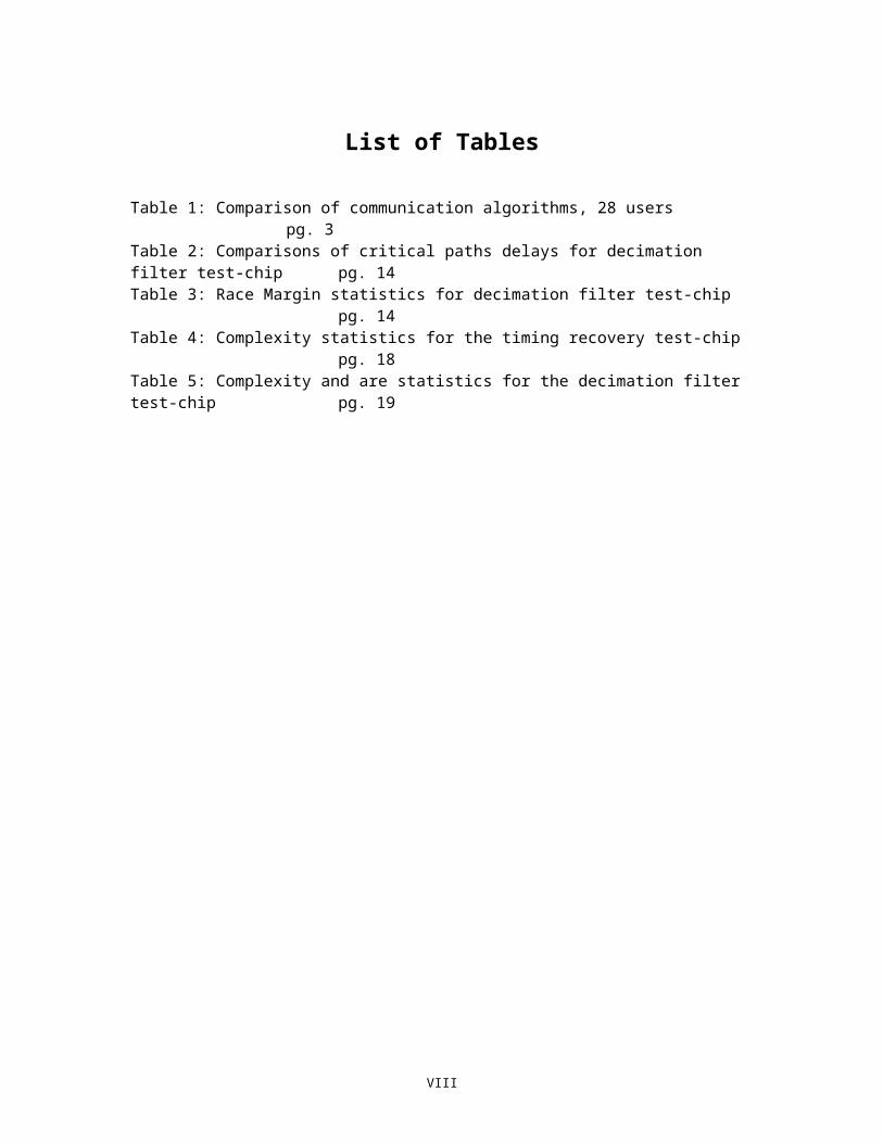
List of Tables
Table 1: Comparison of communication algorithms, 28 users pg. 3Table 2: Comparisons of critical paths delays for decimation filter test-chip pg. 14Table 3: Race Margin statistics for decimation filter test-chip pg. 14Table 4: Complexity statistics for the timing recovery test-chip pg. 18Table 5: Complexity and are statistics for the decimation filter test-chip pg. 19
VII
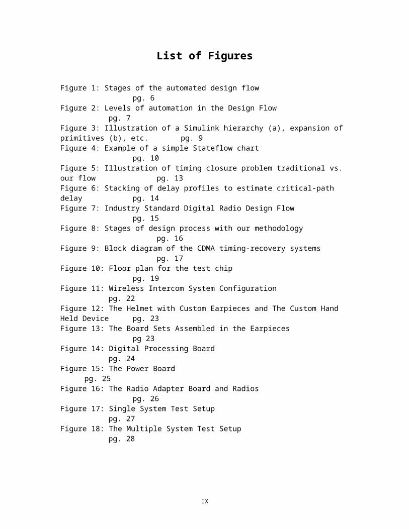
List of Figures
Figure 1: Stages of the automated design flow pg. 6Figure 2: Levels of automation in the Design Flow pg. 7Figure 3: Illustration of a Simulink hierarchy (a), expansion of primitives (b), etc. pg. 9Figure 4: Example of a simple Stateflow chart pg. 10Figure 5: Illustration of timing closure problem traditional vs. our flow pg. 13Figure 6: Stacking of delay profiles to estimate critical-path delay pg. 14Figure 7: Industry Standard Digital Radio Design Flow pg. 15Figure 8: Stages of design process with our methodology pg. 16Figure 9: Block diagram of the CDMA timing-recovery systems pg. 17Figure 10: Floor plan for the test chip pg. 19Figure 11: Wireless Intercom System Configuration pg. 22Figure 12: The Helmet with Custom Earpieces and The Custom Hand Held Device pg. 23Figure 13: The Board Sets Assembled in the Earpieces pg 23Figure 14: Digital Processing Board pg. 24Figure 15: The Power Board pg. 25Figure 16: The Radio Adapter Board and Radios pg. 26Figure 17: Single System Test Setup pg. 27Figure 18: The Multiple System Test Setup pg. 28Figure 19: The Electro Mechanical design of earpiece and hand controller pg. 29Figure 20: Completed Intercom Marine System with Fused deposition Machine pg. 30
VIII
Acknowledgements
Effort sponsored by the Defense Advanced Research Projects Agency (DARPA) and Rome Laboratory, Air Force Materiel Command, USAF, under agreement number F30602-97-2-0346. The U.S. Government is authorized to reproduce and distribute reprints for Governmental purposes notwithstanding any copyright annotation thereon.
This project was also supported by the contributions of and technical discussions with Cadence Design Systems, Ericsson Mobile Systems and Lucent Technologies. STMicroelectronics provided the CMOS fabrication of the test chip. The following graduate students were involved: Rhett Davis, Hayden So, Ben Coates, and Dave Wang on developing the design environment and Paul Hustead on testing the design environment. BWRC technical staff members Sue Mellers and Fred Burghard developed the hardware prototype.
IX

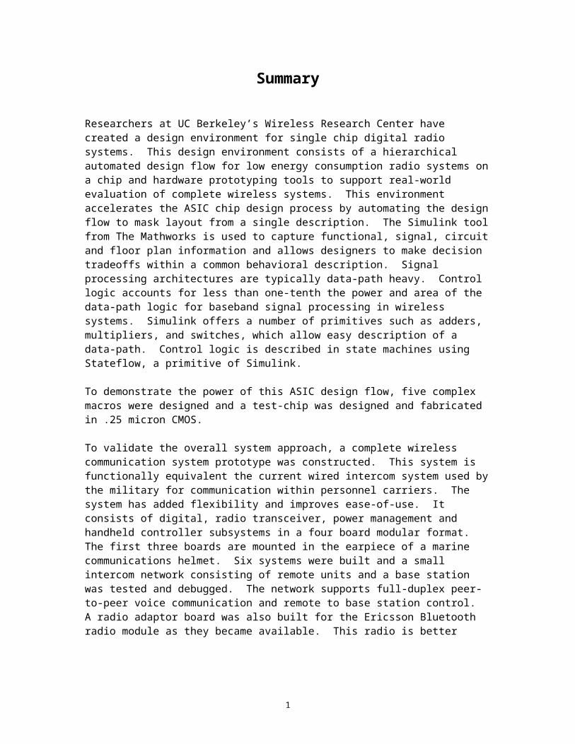
Summary
Researchers at UC Berkeley’s Wireless Research Center have created a design environment for single chip digital radio systems. This design environment consists of a hierarchical automated design flow for low energy consumption radio systems on a chip and hardware prototyping tools to support real-world evaluation of complete wireless systems. This environment accelerates the ASIC chip design process by automating the design flow to mask layout from a single description. The Simulink tool from The Mathworks is used to capture functional, signal, circuit and floor plan information and allows designers to make decision tradeoffs within a common behavioral description. Signal processing architectures are typically data-path heavy. Control logic accounts for less than one-tenth the power and area of the data-path logic for baseband signal processing in wireless systems. Simulink offers a number of primitives such as adders, multipliers, and switches, which allow easy description of a data-path. Control logic is described in state machines using Stateflow, a primitive of Simulink.
To demonstrate the power of this ASIC design flow, five complex macros were designed and a test-chip was designed and fabricated in .25 micron CMOS.
To validate the overall system approach, a complete wireless communication system prototype was constructed. This system is functionally equivalent the current wired intercom system used by the military for communication within personnel carriers. The system has added flexibility and improves ease-of-use. It consists of digital, radio transceiver, power management and handheld controller subsystems in a four board modular format. The first three boards are mounted in the earpiece of a marine communications helmet. Six systems were built and a small intercom network consisting of remote units and a base station was tested and debugged. The network supports full-duplex peer-to-peer voice communication and remote to base station control.A radio adaptor board was also built for the Ericsson Bluetooth radio module as they became available. This radio is better suited for this system since the Intercom application requires lower power consumption and shorter range than the original Proxim radio.
1

Part I – Single Chip Design Software Environment
1. Introduction
The emerging standard for system-on-a-chip (SOC) design flows is well suited to existing portable radio system standards. A state-of-the-art mobile radio transceiver contains a digital base-band chip described by a hardware description language (HDL) and utilizing a small number of intellectual property (IP) blocks such as a digital signal processor, Viterbi decoders, and QPSK demodulators. When we look beyond today’s radio system standards, however, we see that there are still opportunities for vast improvement. Increased bandwidth efficiency comes at a cost of much greater computational complexity, which needs to be provided with low energy in the smallest possible area.
One study of indoor multi-user communication algorithms [1] shows that through the use of multiple antennas and complex signal processing, we stand to gain as much as an order of magnitude better bandwidth efficiency (see Table 1) over a commercially available radio. Unfortunately, the complexity of this algorithm is nearly two orders of magnitude beyond the capacity of an embedded DSP. Given the industry trend towards programmable “software-radios,” it would seem that practical implementation of these algorithms will have to wait many years for embedded processor speeds to catch up. The study also determined that a direct mapping of the most complex algorithms to gates would be well within the capabilities of today’s processing technology (10 mm2, 19 mW). This work focuses on a design methodology for these kinds of direct-mapped signal processing algorithms.
CommercialRadio
Proxim WLAN
CDMAw/ adaptive
MMSE detection
FDMAw/
multipleantennae
bandwidth efficiency
0.3 bps/Hz 1.8 bps/Hz 3.6 bps/Hz
no. of parallel processors
(power)
- 23(303 mW)
87(1149 mW)
direct-mapped area (power)
- 3 mm2
(6.8 mW)10 mm2
(19 mW)direct-mapped
gates- 60K 200K
Table 1: Comparison of communication algorithms for 28 users, 0.8 Msym/sec symbol rate, 15 dB signal-to-noise ratio and 10-5 bit-error-rate. Number of required processors is based on estimates of a low-power 16-bit fixed-point DSP. Direct mapping based on unrouted estimates of a 0.25 um technology operating at 1V and 25 MHz.
2
In order to determine which of the many candidate algorithms is the most practical, we need to evaluate the power and area of their implementations. The complexity of these systems is so great, however, that any method of evaluation other than prototyping tends to be inconclusive. It is not sufficient to stop the design process after the RTL coding phase. The inaccuracy of wire-load models creates too much uncertainty about meeting speed requirements. Therefore, we must develop a design methodology that allows us to map all of the candidate algorithms to silicon for evaluation.
By focusing on the mobile digital radio design problem, we greatly reduce the difficulty of the design flow. Clock distribution is simplified because these chips seldom have clock rates above 100 MHz. Signal integrity problems are minimal even for deep-sub micron technologies due to the low-power, low-voltage nature of the designs. Instead, the challenge for this flow is reduce the design time of a direct-mapped signal-processing algorithm. This paper presents and discusses our design methodology and the first test-chip fabricated with the flow.
2. The Simulink-to-Silicon Design Flow
The central goal of our design flow is to decrease design time. We find that designers spend most of their time in trial-and-error with CAD tools, trying to get the desired output from the available input. By writing scripts to constrain and guide designers’ usage of these tools, we can alleviate this problem only to a point. Over-constrained scripts prevent the designer from truly optimizing the system, while under-constrained scripts are more likely to fail. Some approach must be found to this fundamental problem of CAD tool usage.
If we change our focus from decreasing design time to decreasing re-design time, however, the problem becomes much more straightforward. If a successful path through the CAD tools is found for a certain design, it should be a simple task to capture the flow and re-run it at the push of a button. This decreases the overall design time by accelerating design iterations. To achieve this goal, CAD scripts must not only constrain and guide usage of the particular tool, but also constrain and guide the script’s usage in a more complex flow. This was the organizing principle for the creation of our Simulink-to-Silicon design flow.
Our flow is specified as follows: we want to be able to make changes to a system and observe the effect of these changes on the system performance at the push of a button. For this we had to provide the following:
1. An initial description which captures the changes we would like to make2. A library of primitives which are already well understood and optimized3. Automation spanning several CAD frameworks to generate mask patterns from the initial
description4. A verification methodology to guarantee that the chip will work as described
We furthermore decided that the flow should support arbitrary hierarchy depth. For example, placement and routing should be flat or hierarchical as needed. It is easier to observe the effect of a change if the effect is not distributed throughout the rest of the system. The rest of this section focuses on the problems that had to be solved in order to provide a design flow that meets this specification.
3

We chose Simulink as the input description for our flow because it is inexpensive and often familiar to both algorithm and circuit designers. It is relatively simple to express a design in Simulink, which contains all the detail of a VHDL or Verilog description. The Simulink Fixed-Point Block set allows the description of data-path logic with arbitrary word-lengths. The Simulink Enable block can be used to model a gated clock. State machines designed with Stateflow editor model control logic. User libraries can be created and referenced easily in Simulink, allowing us to describe systems hierarchically. On the whole, Simulink captures the optimizations we wish to make and serves as a complete specification for the functionality of a chip. It is well suited as an initial description for our design flow.
The primitives for our flow were chosen in the context of a base-band CDMA receiver and required the following primitives:
Adder, Subtractor (ripple-carry) Selectable Adder/Subtractor (for CORDIC subsystems) Register Multiplexor Multiplier (Booth-encoded Wallace-tree array) Shifter (Barrel shift) Look-up table Bus ripper Constant value Less than zero
We find that most radio algorithms of interest can be expressed in terms of these primitives. They represent only the highest level of granularity at which we want to design. The automation framework and verification methodology should make the design of more complex primitives as easy as possible. Some conceived examples are finite impulse response (FIR) filters, fast Fourier transform (FFT) processors, and Viterbi decoders. Another optimization that we want our automation framework to recognize is that some primitives do not map to transistors. These wiring primitives include bus rippers, constant values, and less-that-zero operators (sign bits). We now turn our attention to the challenges in providing an automation framework and verification methodology that creates a chip from a Simulink system designed with these primitives.
2.1 Automation Framework
Figure 1 shows the stages of our automated design flow. The elaboration step turns the Simulink system into a transistor-level schematic and a collection of abstract views for routing. This step’s name was chosen because of its similarity to the process of elaborating an RTL design from VHDL code. The next step creates a new floor plan from the schematics and abstracts and merges the information from the previous iteration’s floor plan. This merging is performed by traversing each hierarchy from the top-down, descending into views with matching instance names. This ensures that the merge will be successful as long as the instance names in Simulink did not change between iterations. The last step routes the design from the bottom level of hierarchy to the top and performs design-rule checks (DRC) and layout vs. schematic (LVS) checks as needed.
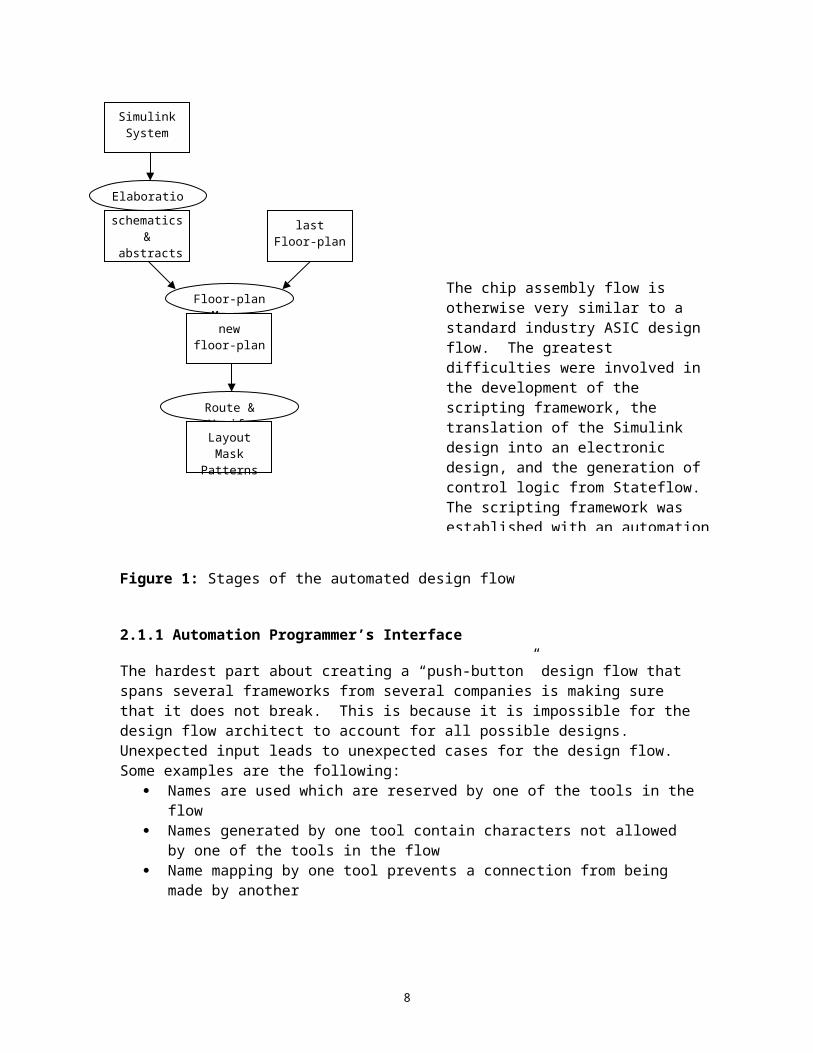
4
Figure 1: Stages of the automated design flow
2.1.1 Automation Programmer’s Interface
The hardest part about creating a “push-button” design flow that spans several frameworks from several companies is making sure that it does not break. This is because it is impossible for the design flow architect to account for all possible designs. Unexpected input leads to unexpected cases for the design flow. Some examples are the following:
Names are used which are reserved by one of the tools in the flow Names generated by one tool contain characters not allowed by one of the tools in the
flow Name mapping by one tool prevents a connection from being made by another One of the tools contains a bug for a particular case of input Floor-plan is too congested and cannot be routed
The price of an unbreakable design flow may be too high. The only way to avoid name conflicts is to choose names that are complex and confusing. Omitting a tool from the flow simply because it contains a bug deprives designers of the power of that tool. Congested floor plans are desirable because they lead to efficient use of area.
If we are not to create an unbreakable design flow, then we can at least create a design flow that breaks with maximum grace. Such a design flow would have the following properties:
Well documented and easily modified Common log file
SimulinkSystem
Elaboration
schematics&
abstracts
Route & Verify
LayoutMask Patterns
lastFloor-plan
Floor-plan Merge
newfloor-plan
The chip assembly flow is otherwise very similar to a standard industry ASIC design flow. The greatest difficulties were involved in the development of the scripting framework, the translation of the Simulink design into an electronic design, and the generation of control logic from Stateflow. The scripting framework was established with an automation programmer’s interface. The electronic design was generated with a home-grown EDIF translator. Control logic was generated with a Stateflow-VHDL translator. The following sections describe these solutions.
5

Robust error trapping mechanism
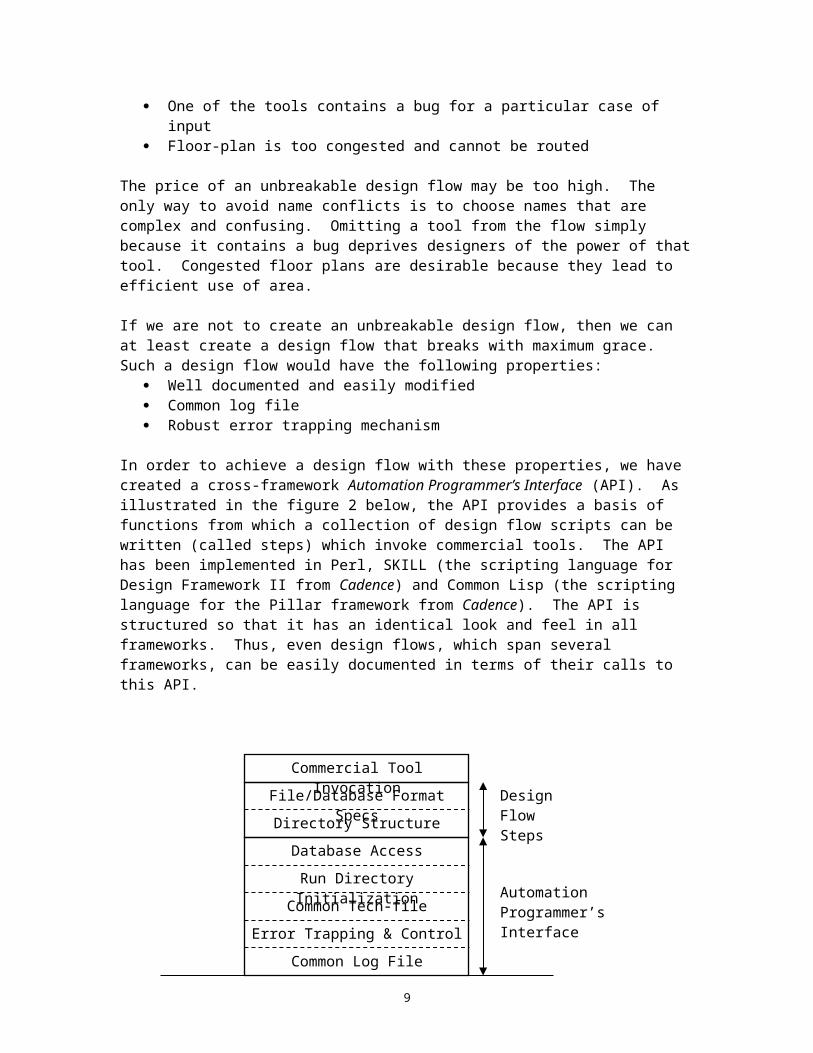
In order to achieve a design flow with these properties, we have created a cross-framework Automation Programmer’s Interface (API). As illustrated in the figure 2 below, the API provides a basis of functions from which a collection of design flow scripts can be written (called steps) which invoke commercial tools. The API has been implemented in Perl, SKILL (the scripting language for Design Framework II from Cadence) and Common Lisp (the scripting language for the Pillar framework from Cadence). The API is structured so that it has an identical look and feel in all frameworks. Thus, even design flows, which span several frameworks, can be easily documented in terms of their calls to this API.
Figure 2: Levels of Automation in the Design Flow
The goal of the API is to take care of the ugliest details of design flow automation while refraining from imposing any file or database formats or assumed directory structure. It is designed in five layers, each layer calling functions implemented in the lower layers. The lowest layer implements the common log file by offering functions to open and close the log-file and print log messages. The functions allow messages to be selectively printed according to a desired level of verbosity. Messages are also indented according to a provided parameter. A set of usage conventions comes with the functions that ensure that log messages are printed to the log file in the proper order.
The next level is the error-trapping and control-flow level that provides a set of functions to begin a step and end a step either successfully or unsuccessfully. A function is also provided to invoke another step within a step. This sub-step can be a design-flow step implemented with the API in any of the three supported platforms, or it can be a generic UNIX program, SKILL or Common-Lisp procedure. In the case of the latter, functions are also provided which scan log files for regular expressions that indicate success or failure of the sub-step. In the case of the former, arguments are passed automatically which ensure the common log file and verbosity are preserved as well as incrementing the indentation level to allow tracking the progress of the hierarchical design flow through the single, common log file.
Common Tech-file
Run Directory Initialization
Database Access
Directory Structure
File/Database Format Specs
Error Trapping & Control Flow
Commercial Tool Invocation
Common Log File
Design FlowSteps
Automation Programmer’sInterface
6
The next two levels provide a common technology file mechanism and a run directory initialization mechanism. The technology file format is very simple and restricted to string types. This is sufficient, since all frameworks offer the means to convert strings to other types. This technology file can be used, among other things, to provide paths to default tool initialization files. Most tools rely on special initialization files in their run directories to set up the technology and libraries. Since the API does not impose a directory structure, it provides the functions to set up run directories for certain tools in arbitrary locations. The API currently supports the following tools:
Synopsys Design Compiler (VHDL synthesis) Synopsys Module Compiler (datapath synthesis) Synopsys EPIC Tools (power estimation, static timing verification) Synopsys Arcadia (parasitic extraction) Cadence Design Framework II (structure processing and netlist generation) Cadence Pillar/Design Planner (floor-planning) Cadence Qplace (placement) Cadence IC Craftsman (routing) Mentor Calibre (physical verification)
The highest level of the API provides a standard means for modifying the design databases. This is not a unified database, since different tools have different databases with different procedural interfaces for modifying them. Instead, the API restricts the structure of code that modifies the database. It creates a special kind of step (called a generator) that opens and modifies a single cell-view in the design hierarchy. Functions for traversal of the entire hierarchy are also provided which use the generator as their building block. The functions act on the database associated with each framework, i.e. SKILL generators act on the Design Framework II database, common-lisp generators act on the Pillar database. Perl generators also act on the Design Framework II database through the use of SWIG [1] wrappers for C-based access functions provided by Cadence.
By implementing our design flow in terms of this API, we have been able to create one 300k transistor chip in 0.25 um technology (described later) and are maximally reusing the code as we extend the flow to handle larger, more complex chips in 0.18 um and 0.12 um technologies. By periodically re-running the flow on a set of reference designs, we have gained a few residual benefits:
Existence of a working example for every tool in the design flow. This helps to educate new team members about the usage of certain tools.
Ability to exchange old tool versions with new tool versions in a matter of hours. The design is re-executed at the push of a button, and inconsistencies between versions are flushed out in the process.
2.1.2 Simulink-EDIF Translator
The first major task in the implementation of our design flow was the development of a way to translate the Simulink design into an electronic design. We decided that a structural mapping was favorable to a behavioral mapping because it is simpler and gives us more freedom when optimizing our primitives. This is similar to the approach used by the Hardware Design System (HDS) extension to Cadence’s SPW [1] which provides a library of special primitives which map
7

to VHDL or Verilog code. We therefore created a Simulink-to-EDIF translator, since EDIF is the most common and generic format for representing structural design data. This translator relies on the Simulink fixed-point block-set types to specify bus widths and the Simulink subsystem to specify hierarchy.
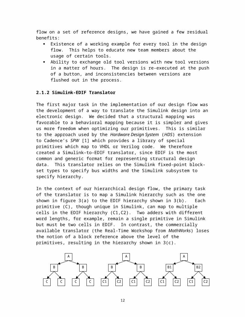
In the context of our hierarchical design flow, the primary task of the translator is to map a Simulink hierarchy such as the one shown in figure 3(a) to the EDIF hierarchy shown in 3(b). Each primitive (C), though unique in Simulink, can map to multiple cells in the EDIF hierarchy (C1,C2). Two adders with different word lengths, for example, remain a single primitive in Simulink but must be two cells in EDIF. In contrast, the commercially available translator (the Real-Time Workshop from MathWorks) loses the notion of a block reference above the level of the primitives, resulting in the hierarchy shown in 3(c).
(a) (b) (c)Figure 3: Illustration of a Simulink hierarchy (a), expansion of primitives (b), and loss of
reference information above the primitives with RTW (c)
From an automation standpoint, figure 3(c) is better. It can be difficult to define what it means for two blocks to be functionally equivalent, so the more robust automation strategy is to make every block unique. From an optimization standpoint, however, figure 3(b) is better. If we wish to examine the performance trade-off for two implementations of block B, for example, it is much easier to simply modify B than to modify every instance of B in the hierarchy. Our hierarchy mapping was a compromise of the competing needs for automation and optimization. We eventually settled on the following two rules:
Rule 1: Two instances of a Simulink primitive become instances of the same EDIF cell if all ports have the same fixed-point types all distinguishing parameters have equivalent values
Rule 2: Two instances of a Simulink subsystem become instances of the same EDIF cell if all of their contained primitives map to the same EDIF cells.
The first rule states that, aside from port types, it is the job of creator of the primitives to decide what parameters distinguish functionally equivalent blocks. For example, a parameter, which sets the number of cycles of latency for a multiplier, distinguishes functionally different blocks. A parameter, which sets the cycle time for a register, distinguishes a connection to a different clock but does not make the blocks functionally different.
One very important repercussion of these rules is that traditional methods of optimization, such as driver-load balancing, no longer work above the level of the Simulink primitive. This is because
C C
B
C C
B
A
C1 C2
B1
C1 C2
B2
A
C1 C2
B
C1 C2
B
A
8

circuit parameters such as loading are not a factor in determining the equivalency of blocks. This encourages us to use primitives that traditional synthesis tools optimize well and leave all other optimization up to the chip designer.
2.1.3 Stateflow-VHDL Translator
Another major obstacle for our design flow was a strategy for handling control logic. Unlike data-path logic, control logic tends to be quite unstructured and is seldom reused between chip projects without modification. Given the difficulty of verifying functional equivalency between Simulink primitives and their implementations, it is unreasonable to expect that a new primitive will be designed for every new piece of control logic. We therefore created a primitive around the Simulink Stateflow chart.
Simulink Stateflow is a graphical language for describing control flow with state machines, based almost entirely on the StateCharts language developed by Harel [1].The primary challenge for this translator is to distill a synthesizable VHDL hardware state-machine from a software state machine. The difficulty of translating a software state machine into hardware can be better understood by examining the simple Stateflow chart shown in figure 4. This chart shows an output signal called count that is modified upon entering one state or simply by remaining in another state (specified by the “during” key word). In contrast, a hardware state machine uses combinational logic to determine the next state and output from the current state and input. This contradicts the Stateflow chart in which the output changes even though the current state and input do not.
Figure 4: An example of a simple Stateflow chart that counts from 0 to 7 and restarts from zero if the input signal sat_en is low or stays at 7 while sat_en is high.
9
Our goal was generate a hardware state machine that was as efficient as possible while remaining functionally equivalent to Stateflow. We expressed this goal as the following optimization rule:
Optimization Rule: The hardware should contain a number of flip-flops equal to Log2 of the number of states plus the minimum amount of storage for variables.
Once this optimization rule was chosen, the creation of the VHDL code was a matter of declaring memory signals for the states and variables and reverse engineering the Stateflow execution model in a single VHDL process. We rely on synthesis tools to map the VHDL process to efficient combinational logic. The translator accepts a subset of the Stateflow syntax. Some constructs not supported by the translator are the following:
Transition actions (all data must be set within a state) State exit actions (all data must be set with an “entry” or “during” action) Some types of hierarchical state machines Variable shift operations on dataAlthough we have not yet found reliable mappings of these constructs to VHDL, no
fundamental barrier to their translation is known.
One of the biggest difficulties for this methodology was the implementation of a reset condition. In hardware, a reset is implemented by setting the values of all registers (i.e. the current state and variables) to some known value. In Stateflow, however, the reset is indicated by a transition rather than a state, as indicated by the large black dot in the upper left corner of figure 4. We solved this problem by adding to the VHDL code a synchronous transition from every state to the initial state, depending on the value of a global “Stateflow reset” signal.
The translator was verified through implementation of four state machines the a timing recovery test-chip. The Stateflow charts ranged in complexity from 5 to 27 states, 4 to 35 ports, and 0 to 30 bits for variables. Functionality was verified by cross-simulation of the entire system in Simulink and EPIC TimeMill. Implementing one of the smaller state machines in hand-coded Verilog tested the hardware efficiency. It was found that the hand-coded version, though significantly less verbose, was 20% larger in terms of cell area after synthesis. We have therefore come to rely on the Stateflow chart and its VHDL translator as an efficient primitive for our automated design flow.
2.2 Verification Methodology
In order for our Simulink-to-Silicon methodology to be viable for system optimization, we need to be able to provide guarantees that a certain change will result in functional hardware. The automated flow uses flat DRC and LVS checks on the final mask patterns to ensure that placement and routing were successful. A scan-chain is automatically inserted to allow for testing of fabricated chips. Signal integrity problems are assumed to be negligible due to the low-power, low-speed nature of the digital radio design space. The problems of function and timing verification, however, can be serious stumbling blocks. In this section, we discuss our approach to these problems.
10
2.2.1 Function Verification
Since the Simulink system is our complete specification for the behavior of a system, the resulting hardware must be functionally equivalent. Anything less than equivalency would lead to optimizations, which “might” be feasible, which means that we could not reliably answer questions about hardware efficiency. In the absence of formal methods to verify functional equivalency between Simulink and transistor-level descriptions, we are left with simulation.
Assuming that the Simulink-EDIF translator is bug-free, the problem reduces to the matter of proving functional equivalency of Simulink primitives to their hardware implementations. We used EPIC TimeMill simulations of our timing-recovery test design to debug our primitives. Our primary problem was that the Simulink Fixed-Point Block set’s method of truncating most- and least-significant bits is not clearly defined. In the end, we were still unable to provide functional equivalency for all combinations of fixed-point types. We therefore adopted the following rules to guarantee functional equivalency:
Rule 1: Each primitive has a set of rules which specify legal fixed-point types for ports. For example, an adder with a 12-bit unsigned integer input port must have the same type for the other input port and a 13-bit unsigned output port.
Rule 2: Sign extension, zero filling, and MSB and LSB truncation are always performed by specially verified blocks, never in an arithmetic block (such as an adder or multiplier).
A simple tool was created for the purpose of scanning a Simulink design and providing fast feed-back about the observance of these rules. For systems which use our primitives and follow these rules, we have not yet observed the case where the Simulink and transistor-level descriptions are functionally different. An alternative to these rules exists for primitives implemented in design systems which provide automatic test-pattern generators (ATPG). For these primitives, a complete set of test patterns which can be used to verify the functional equivalency of a Simulink. Due to the overhead of supporting ATPG, however, this approach has not yet been attempted.
2.2.2 Timing Verification
In order to guarantee the functionality specified by the Simulink system, we must provide assurance that the assumed cycle time can be met and that no races exist between registers. These conditions are typically checked by generating a set of setup and hold time constraints for every path between registers and using static timing models to verify that the constraints are met. The process of adjusting a design to meet the constraints is commonly called timing closure.
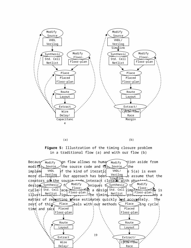
The timing closure problem is very different in our design flow from the traditional ASIC flow. The traditional flow expects that the creators of the source code for a design have little or no interaction with those performing the physical design. As a result, the physical design industry has come to rely heavily on tools which iteratively search for mask layout which meets the setup and hold time constraints. Figure 5(a) illustrates the standard process of extracting wiring delay or capacitance values from a routed design and using these values for re-routing, re-placing, or re-synthesizing. The timing closure problem becomes a matter of finding a successful iterative path
11

through the tools. Modifying the source code is a last resort because it represents the largest delay in the design process.
12

(a) (b)
Figure 5: Illustration of the timing closure problem in a traditional flow (a) and with our flow (b)
Because our design flow allows no human intervention aside from modification of the source code and floor plan, the implementation of the kind of iteration in figure 5(a) is even more difficult. Our approach has been instead to assume that the creators of the source code interact closely with physical designers and to focus on techniques that report the minimum cycle-time and race margin for a design. This simplified flow is illustrated in figure 5(b). The timing closure problem becomes a matter of reporting these estimates quickly and accurately. The rest of this section deals with our methods of estimating cycle time and race margin.
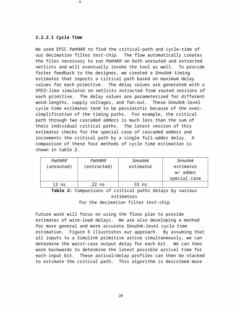
2.2.2.1 Cycle Time
We used EPIC PathMill to find the critical-path and cycle-time of our decimation filter test-chip. The flow automatically creates the files necessary to run PathMill on both unrouted and extracted netlists and will eventually invoke the tool as well. To provide faster feedback to the designer, we created a Simulink timing estimator that reports a critical path based on maximum delay values for each primitive. The delay values are generated with a SPICE-like simulator on netlists extracted from routed versions of each primitive. The delay values are parameterized for different word-lengths, supply voltages, and fan-out. These Simulink-level cycle time estimates tend to be pessimistic because of the over-simplification of the timing paths. For example, the critical path through two cascaded adders is much less than the sum of their individual critical
Modify Source
VHDLVerilog
Modify Floor-plan
Floor-plan
Synthesize
Std. CellNetlist
Place
PlacedFloor-plan
Route
Layout
Extract
Wire Delay/Capacitance
Modify Source
VHDL/VerilogSimulink
Modify Floor-plan
Floor-plan
Synthesize
Std. CellNetlist
Place
PlacedFloor-plan
Route
Layout
Cycle TimeRace Margin
Extract/Analyze
Modify Source
VHDLVerilog
Modify Floor-plan
Floor-plan
Synthesize
Std. CellNetlist
Place
PlacedFloor-plan
Route
Layout
Extract
Wire Delay/Capacitance
Modify Source
VHDL/VerilogSimulink
Modify Floor-plan
Floor-plan
Synthesize
Std. CellNetlist
Place
PlacedFloor-plan
Route
Layout
Cycle TimeRace Margin
Extract/Analyze
13
paths. The latest version of this estimator checks for the special case of cascaded adders and increments the critical path by a single full-adder delay. A comparison of these four methods of cycle time estimation is shown in table 2.
PathMill(unrouted)
PathMill(extracted)
Simulink estimator Simulink estimatorw/ adder special case
13 ns 22 ns 33 nsTable 2: Comparisons of critical paths delays by various estimators
for the decimation filter test-chip
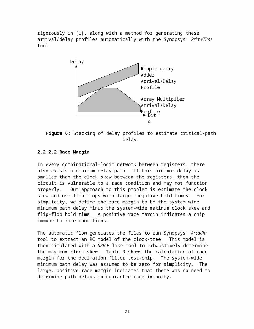
Future work will focus on using the floor plan to provide estimates of wire-load delays. We are also developing a method for more general and more accurate Simulink-level cycle time estimation. Figure 6 illustrates our approach. By assuming that all inputs to a Simulink primitive arrive simultaneously, we can determine the worst-case output delay for each bit. We can then work backwards to determine the latest possible arrival time for each input bit. These arrival/delay profiles can then be stacked to estimate the critical path. This algorithm is described more rigorously in [1], along with a method for generating these arrival/delay profiles automatically with the Synopsys’ PrimeTime tool.
Figure 6: Stacking of delay profiles to estimate critical-path delay.
2.2.2.2 Race Margin
In every combinational-logic network between registers, there also exists a minimum delay path. If this minimum delay is smaller than the clock skew between the registers, then the circuit is vulnerable to a race condition and may not function properly. Our approach to this problem is estimate the clock skew and use flip-flops with large, negative hold times. For simplicity, we define the race margin to be the system-wide minimum path delay minus the system-wide maximum clock skew and flip-flop hold time. A positive race margin indicates a chip immune to race conditions.
The automatic flow generates the files to run Synopsys’ Arcadia tool to extract an RC model of the clock-tree. This model is then simulated with a SPICE-like tool to exhaustively determine the maximum clock skew. Table 3 shows the calculation of race margin for the decimation filter test-chip. The system-wide minimum path delay was assumed to be zero for simplicity. The large,
Bits
DelayRipple-carry AdderArrival/Delay Profile
Array Multiplier Arrival/Delay Profile
14
positive race margin indicates that there was no need to determine path delays to guarantee race immunity.
Maximum Clock Skew Flip-flop Hold Time Race Margin5 ns
Table 3: Race Margin statistics for the decimation filter test-chip
It remains to be seen how large the chips can be before this method breaks down. Future work will explore the design of larger chips and a technique for early estimation of clock skew from the Simulink design and floor plan.
2.3 Comparison to Industry Standard Flow
Let us compare our methodology to a more standard design flow. Consider the design of a digital receiver for a third-generation indoor wireless network. The data rates will high (2-3 Mbps) and the power budget very low due to battery life constraints. Extensive signal processing will be required due to the unfriendly indoor wireless environment (multi-path echoes) and multi-access interference from other users. The challenge of the design process is to create a chip that meets the performance specifications while keeping the area and power at a minimum.
Figure 7: Industry Standard Digital Radio Design Flow
As shown in figure 7, common industry practice is to break the chip design into three phases handled by three different engineering teams. The divisions between these phases are so well understood that they can even be distributed between different companies. The chip vendor performs the system design and delivers a specification to the ASIC design house in the form of a
System Design
ASIC/Front-End Design
Physical/Back-End Design
MatlabC
SPW
VHDLVerilog
LayoutMask Patterns
15
simulation. Matlab code, C code, and Cadence SPW designs are some of the most common formats for this simulation. The simulation contains a rough block-diagram of the system with functional blocks such as Viterbi decoders, adaptive equalizers, multi-path echo cancellers, and timing-recovery systems. These functional blocks are designed with primitives, which range in complexity from adders, registers, and multipliers up to FIR filters and Fast Fourier Transform (FFT) processors. This simulation can be used to generate a bit-error-rate vs. signal-to-noise ratio (BER vs. SNR) characteristic that the system designer expects the ASIC designer to meet.
The ASIC design team uses the simulation to create a VHDL or Verilog design, which it delivers to the physical design house. The ASIC designer is free to choose any implementation for the primitives used in the simulation. Adders can ripple-carry or carry-look ahead, array or serial multipliers can be used depending on the timing and latency requirements. Complex primitives such as FFT’s offer the most opportunity for optimization. Optimization beyond the primitives is discouraged, however, because it runs the risk of yielding a worse BER vs. SNR characteristic.
The physical design team synthesizes and maps the VHDL or Verilog code to a standard-cell library and uses place route tools to generate layout mask patterns for fabrication. The code must meet all of the requirements for successful synthesis, clock-tree insertion, and timing verification. More advanced ASIC design teams deliver chip floor plans, but in general it is the physical designer’s job to create a floor plan. The physical designer must guarantee that fabricated chip will match the functionality of the VHDL or Verilog description.
Since time-to-market constraints are so critical to the success of a chip project, designers are focused on the task of making sure that this pipeline does not stall. There is not enough time for multiple passes through this flow in search of a design with less power consumption and area. As a result, system designs are less aggressive to give flexibility to ASIC designers. ASIC design is less imaginative because it needs to meet BER vs. SNR requirements as well as the physical format requirements. The physical design remains as highly constrained as possible to give more freedom to ASIC designers.
Figure 8: Stages of the design process with our methodology
System Design
ASIC Design
Automated Flow
BehavioralSimulinkSystem
StructuralSimulinkSystem
LayoutMask Patterns
Macro Design
Physical Design
NewSimulinkPrimitives
FloorPlan
16
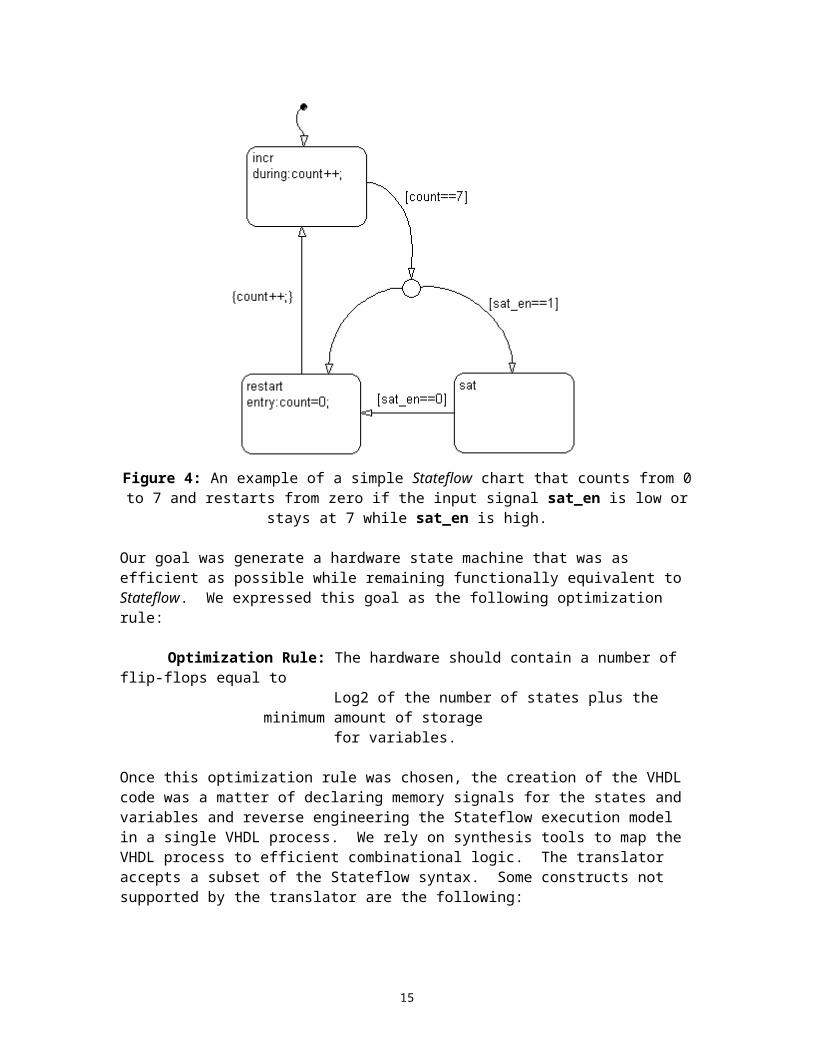
Figure 8 shows how the design process changes with the application of our methodology. The first notable difference is that the automated flow must exist on one computer system and cannot be spread across three companies as before. The second difference is that system, ASIC, and physical designers are forced to work together to produce a design which will pass successfully through the automated design flow.
System designers now produce a Simulink simulation as a specification for the chip. ASIC designers must map this system to a structural Simulink system in terms of the available primitives. If new primitives are needed, they must be designed in VHDL or Verilog along with a functionally equivalent Simulink block. Physical designers work with ASIC designers to produce a floor plan at the same time that the structural Simulink design is being developed.
Once a single pass through the automated flow has been achieved, the structural Simulink system and floor plan can be altered and the mask-patterns regenerated at the push of a button. Alternative macro designs can be substituted and evaluated. The similarity between the behavioral and structural Simulink systems makes it easier to explore modifications to the system that achieve the same (or better) BER vs. SNR characteristic.
3. Test Chips
Our Simulink-to-Silicon flow was originally developed in the context of an indoor, wireless CDMA system created in-house. The system supports 14-users at 3.2 Mbps/user with a code length of 15 and chip rate of 25 MHz, described more fully in [1]. Our flow was used on two test-chips, which are subsystems of the base-band receiver. A block diagram for the first test-chip is shown in figure 9. This system is intended to provide coherent timing recovery and code acquisition in a multi-user-detection receiver system and is described in more detail in [2]. The system expects 8 parallel streams of data from the A/D converter, each representing a timing offset of 1/8 of a chip. To generate these streams, an 8x parallel decimation filter for the sigma-delta converter was also designed and included on the test-chip.
Figure 9: Block diagram of the CDMA timing-recovery system for which the flow was originally developed (A/D converter was designed outside this flow)
Sigma-DeltaA/D
Converter
PilotAcquisitionAnd Coarse
Timing
(Adaptive)Data
Correlator
DigitalPhase
LockedLoop
Fine TimingAnd Carrier
OffsetEstimation
MUX8
3
3 1
MUX
17
Complexity statistics for the timing-recovery test-chip are shown in table 4. It was built primarily with tiled, hard-macro primitives that we call modules. The module generators were implemented in SKILL using custom leaf-cells. The Stateflow and look-up table primitives were implemented as soft-macros.
macro name no. of versions
no. of instances
total xstrs total cell area mm2
Register 30 632 239,976 2.49Add 49 721 181,748 0.98Multiply 4 20 86,798 1.26Subtract 16 226 64,070 0.34Add/Subtract 25 47 22,868 0.15MUX 6 42 5,160 0.03Barrel Shift 4 12 2,680 0.02Other 6 61 4,620 0.03all modules 140 1714 607,920 5.3
lookup tables 3 3 403 0.002Stateflow 6 7 17,725 0.11all soft macros 9 10 18,128 0.11
clock buffers 24 24 2,320 0.09
Total 149 1724 628,368 5.5
Table 4: Complexity statistics for the timing recovery test-chip
As can be seen from these statistics, data-path elements are the most heavily used. The fact that the ratio of versions to instances is small indicates that the Simulink-EDIF translator is effectively expanding the primitives. The complete flow for this design (not including routing and verification) runs in about 30 minutes on a Sun Ultra-4 processor with 4 GB of swap space.
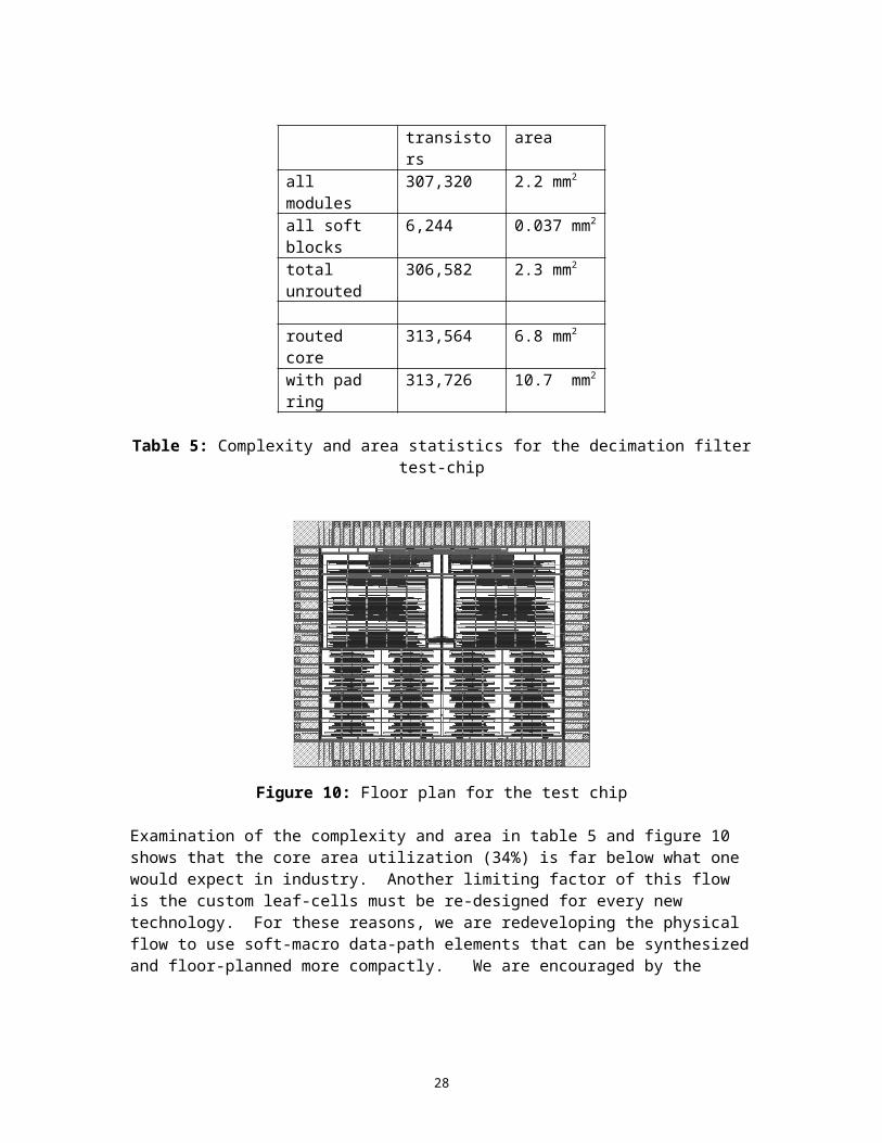
Due to the complexity of the timing-recovery design, only its primitives were carried through the entire flow to mask layout. The complete system was verified functionally but never routed. To test the automatic physical design flow, a second test-chip was fashioned around the decimation filter subsystem. The decimation filter is roughly the same size as the timing-recovery system but uses only 5 primitives. This system was carried through the complete flow and fabricated in a 0.25 um technology. Complexity statistics for this test-chip are shown in table 5, along with a floor plan in figure 10. The complete flow for this chip runs in about 70 minutes with all but 10 minutes required for routing and verification.
18
transistors areaall modules 307,320 2.2 mm2
all soft blocks 6,244 0.037 mm2
total unrouted 306,582 2.3 mm2
routed core 313,564 6.8 mm2
with pad ring 313,726 10.7 mm2
Table 5: Complexity and area statistics for the decimation filter test-chip
Figure 10: Floor plan for the test chip
Examination of the complexity and area in table 5 and figure 10 shows that the core area utilization (34%) is far below what one would expect in industry. Another limiting factor of this flow is the custom leaf-cells must be re-designed for every new technology. For these reasons, we are redeveloping the physical flow to use soft-macro data-path elements that can be synthesized and floor-planned more compactly. We are encouraged by the success of this chip and are now focusing on the task of demonstrating this methodology on a chip in the 1-10 million-transistor range.
19

Part II - Hardware Implementation
1. Project Goal
A wireless communication system prototype was constructed as a functional alternative to existing wired intercom system used by the Marines for communication within armored vehicles. The requirements of the Marine Intercom were for a multi-station network with high-quality voice communication that could be configured to meet soldier-to-soldier communication needs under high ambient noise field operational conditions. The system also adds flexibility and improves ease-of-use through the use of an imbedded microcontroller. Figure 11 shows the system configuration.
2. Hardware System DescriptionThe wireless intercom system is a single cell system. Each mobile has a frequency-hopped radio with a data rate of 1.6Mbps. Channelization is provided through a time division multiple access scheme. Voice communication is from node-to-node and is not processed through the base station. Each conversation is full duplex with a rate of 64 Kbps, which when combined with control data gives a cell capacity of approximately 20 users. The base station maintains control of the system, such as handling the set-up of new conversations and the allocation of resources, and may be implemented by a mobile unit switching into base station mode, or it can be a separate fixed unit.
3. Intercom Hardware Design OverviewThe hardware is relatively simple due to the two core system components, the StrongARM SA-1100 CPU and the Xilinx FPGA. The highly integrated nature of the StrongARM and the flexibility of the Xilinx allow peripherals to be directly interfaced to both devices.
The StrongARM and the Xilinx form the heart of the system. With the exception of the analog front-end (codec) chip and the radio, all input/output is tied directly to the StrongARM.
Audios input (microphone) and output (speakers) are connected directly to the multipurpose codec chip, which communicates with the StrongARM through a synchronous serial Multimedia Communications Port. Upon receiving information the codec will trigger an interrupt at the StrongARM through a dedicated IRQ signal. The StrongARM then passes this information (after any necessary processing) to the Xilinx, which is memory mapped into the StrongARM’s address space. The StrongARM reads and writes information to and from the Xilinx like a bank of registers. The data path between the Xilinx and the StrongARM is 32 bits, with 8 bits of addressable space. The Xilinx, which has its own memory for buffering, FIFOs and look-up tables, packetizes the data and sends it to the radio in accordance with its protocols. Finally the radio transmits the data. Data, which is received at the radio, follows the opposite of the path just described. The radio provides an analog Received Signal Strength Indicator (RSSI) signal that is directed to one of the A/D converters on the codec chip. This gives the intercom an idea of the channel state, which it can use to modify its algorithms to improve performance.Not including the 1 MB of memory dedicated to the Xilinx, the intercom has a total of 8 MB of memory. 4 MB of Flash memory, which is used to store boot code, programs, and other permanent information. The remaining memory consists of 4 MB of DRAM.
20
The intercom is also equipped with two external serial ports. One is an RS-232-like serial port that can communicate at 230 Kbps and is integrated with the StrongARM. This UART can be used to program the Xilinx from a laptop, update the intercom’s firmware, or enable the use of ARM’s development software. The second serial port is a 12 Mpbs Universal Serial Bus (USB), which is also integrated on the StrongARM. This is intended to be used as a backbone connection between the base station and a PC or other device.
Four general purpose input signals to the StrongARM (as well as power and ground) are brought out to an external connector. This auxiliary input port is used for prototyping different input devices (i.e. the Hand Held Device), which serves as the primary interface to the intercom in the final version.
4. Accomplishments
A preliminary version, Phase 1, of the Marine intercom was demonstrated at the June 1998 DARPA PI meeting. It consisted of a Motorola two-way radio installed in a Marine helmet validating the physical aspects of a single-station setup and first order multiple-unit communication via limited channel selection. The operator was able to communicate with a second mobile while wearing the Marine helmet.
The final Intercom system, Phase 2, consisted of two major parts:
The physical aspects of a unit for a single station i.e. custom-designed helmet earpiece enclosures and custom circuit boards installed in the enclosures, and a hand-held unit with push buttons for power, push-to-talk, and mode selection. The enclosures were designed and build by the Integrated Manufacturing Lab in Mechanical Engineering at U.C. Berkeley. The boards were designed by the Berkeley Wireless Research Center and subcontracted for production.
Software and configurable logic was used to implement peer-to-peer voice channels and control protocols. The control protocols provided a high degree of flexibility for network configuration. Voice communication could be point-to-point between users, a conference between multiple and arbitrary sets of users, multicast, or broadcast from an arbitrary station. System configuration could be set by a privileged user and could be modified instantaneously from a control console. Conversations could be initiated or terminated by use of “no-look” combinational manipulation of four buttons on the hand-held unit, limited by network restrictions imposed by the privileged user (e.g. commander). For instance, broadcast could be a command-only capability, listen in or break into a conversation could be limited to certain individuals. The system supported eighteen users, each with a dedicated 64Kbps of bandwidth for voice. All software and FPGA designs were done by the Berkeley Wireless Research Center.
All earpiece-mounted boards of the phase 2 Intercom system are complete and fully tested. Figure 12 shows the helmet complete with the earpieces and hand held device. The boards assembled into the earpieces are shown in figure 13. The board system includes a digital subsystem board with an ARM processor and Xilinx FPGA, an adapter board for the Proxim Rangelan II radio, and a power board which supplies the required regulated voltage levels for the
21
digital system and the radio. Figure 14 describes the digital processing board. The power board is described in figure 15. The radio adapter board and radios are described in figure 16. There are currently six units in operation, each composed of the three boards plus a radio. A small Intercom network consisting of several remote units and a base station have been tested and debugged. The network supports full-duplex peer-to-peer voice communication and remote to base station control.
We have also designed and built an adapter board for the Ericsson Bluetooth radio module. This radio is better suited for our purposes, since the Intercom application requires lower power consumption and shorter range than offered by the Proxim.
Two Chip Intercom (TCI) is a continuation of research from Intercom that is targeting a dual chip implementation of the Intercom architecture and protocols. The TCI system consists of a single digital chip and a companion analog (RF) chip. The digital chip will contain a Tensilica Xtensa processor, an embedded FPGA, and custom logic interconnected with a Sonics configurable back plane.
To leverage the effort put forward for Intercom, a comprehensive development environment has been created that allows a researcher to create and test generic applications for a low power piconet using Intercom-derived hardware and software.
Tasks remaining for a fully functional system include design and implementation of the electrical components for a manual control unit (the enclosure for this unit has been built), full integration of the hardware into the helmet, and final test and debug of several advanced protocol features.
All major hardware elements of the Intercom prototype have been completed. All basic software components have also been completed and tested. We have successfully demonstrated a three-unit Intercom system on the bench, with peer-peer voice communication. Figure 17 shows a test setup for testing a single system. A multiple system test setup is shown in figure 18. Figure 19 explains the development of the casing using a fused deposition modeling rapid prototyping system for fabrication. A complete intercom system is being worn in figure 20.
22
23

The System Boards1. Digital Board
StrongArm1100/Xilinx/Memory Board Xilinx external RAM and ROM to support protocol research Complete CPU subsystem
2. Power/Codec/Connector Board Switchable Power Supplies to 3.3v, 5v, and 1.5v External Control Interface; connectors to Radio board and Hand Held Device Audio Interface
3. Radio Adapter Board Connector adapter for Proxim RangeLANII Radio or Bluetooth Single Chip Radio
4. Hand Held Device Board Mode switches/ volume adjust/ On/ Off/ Push to Talk/ 2 AA Batteries
Figure 12: The Helmet with Custom Earpieces and The Custom Hand Held Device
Figure 13: The Board Sets Assembled in the Earpieces
24

Digital Processing Board Features
Complete CPU subsystem and FPGA System Reset DRAM (1M x 16) x 2 FLASH Memory (1M x 16) x 2 Xilinx with SRAM (256K x 26), Flash Memory (256K x 16), PROM for serial
configuration (512K x 1) Board to Board Connectors
Figure 14: Digital Processing Board
Component Side Solder Side
25

Power/ Debug Board Features Maxim Power Level Converters:
o 3.3 volts dedicated to StrongArmo General 3.3 voltso 1.5 voltso 5 volts
Transceiver for serial connector Board to Board connector Debugging connectors: serial, address, and data busses Codec Interface Hand Held Device Connector Radio Adaptor Board Connector
Figure 15: The Power Board
Component Side Solder Side
26

Radio Adapter Board Test connector Radio connector Board to board connectors Prototyping area
Figure 16: The Radio Adapter Board and Radios
ProximRangeLANII Radio
Bluetooth Radio
Adapter Board - Solder SideAdapter Board - Component Side
27
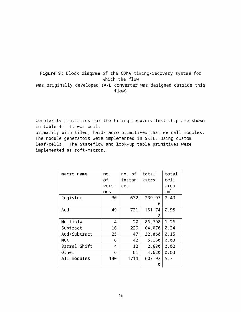
Figure 17 shows a complete single test setup with the laptop running the arm development system. This software is downloaded into the StrongArm and Xilinx through a serial port. Audios input and output are through the headsets connected to the digital board. A codec on the digital board translates the audio signal to a digital signal ready for input and processing at the StrongArm.
Figure 17: Single System Test Setup
28
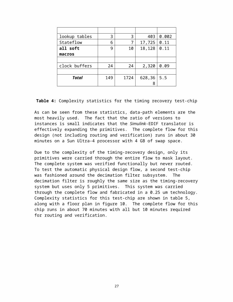
Figure 18 shows a complete test setup of two Intercom Systems talking to each other through Proxim RangeLan2 radios. Each setup has their own headset for listening and voice input as well as a laptop for independent downloading of custom software. The custom software is for system control as well as running custom applications.
Figure 18: The Multiple System Test Setup
Laptops
Oscilloscope
Digital Analysis System
Audio I/O
29
Fabrication Method using Fused Deposition Modeling
The process of fused deposition modeling involves decomposing a 3D object into slices. A nozzle traverses the area of an individual slice, feeding out strands of molten plastic. The part is then built from the ground up with each completed slice.
Fused deposition modeling is a rapid prototype method. Fabrication time for this intercom case took approximately 10 hours. With this method, one is able to use many different types of plastic resins. The result is a tough, working prototype with 70% porosity.
Figure 19: The Electro Mechanical design of earpiece and hand controller for Marine Corps communications system
30

Figure 20: Completed Wireless Intercom System Integrated into a Marine Helmet next to the Fused Deposition Machine used for Prototype Case Fabrication
31
Results and Discussion
This project has demonstrated that it is possible to design and implement a wireless system to meet the specifications of the Marine Intercom system. Prototype wireless systems were built and tested in peer-to-peer and wireless Intercom network mode.
An environment to support rapid design of single chip, low power wireless systems was developed and a test chip was produced to validate the basic approach. The success of the test-chip and ease of the macro hardening flow are encouraging. The next step is to apply the flow to the design of systems in the 1M to 10M-transistor range. The most difficult aspect of this flow is the verification of functional equivalency of macro generators and their Simulink models. As macros become more complex, more opportunities for discrepancy arise, leading to potential problems when macros are combined. Future work will focus on comparisons of the estimates gained from this approach to estimates made with other system-level design methods. Also, much more investigation is needed into the level of detail needed during floor planning and into which macro granularities scale best to future process generations.
All major hardware and software elements of the Intercom prototype have been completed and tested. A three-unit Intercom system was successfully demonstrated for peer-to-peer voice communication and in mobile-base station networked communication. The remaining tasks for the prototype are to design and implement the electrical components for a manual control unit (the enclosure for this unit has been built), and final test and debug of several advanced protocol features.
This project has shown that digital radio chips can be designed using the single chip environment tools that have been created. Furthermore, a complete wireless Intercom system has been demonstrated. The final single chip digital radio was not implemented due to cancellation of funding for this work.
32

Conclusions
A design environment for single chip digital radio systems has been developed and a prototype system was been built and tested. The design environment was validated through the design and fabrication of a CMOS decimation filter test chip. The foundation of the basic approach to the
design of single chip digital radios has been validated. A large research effort has gone into creating the foundation design systems that are captured in this report. However, much work
remains to be done; including; demonstrating the design tools on chips in the 1-10 million transistor range, integration of a complete digital radio on one chip and constructing a complete wireless communications system using the chip. These tasks are being pursued at the Berkeley
Wireless Research Center and further funding is being solicited to support extensions of this work.
33
References
[1] R. Brodersen, “The network computer and its future,” Proc. of the 1997 International Solid State Circuits Conference.
[2] N. Zhang, et al., “Trade-offs of performance and single chip implementation of indoor wireless multi-access receivers,” Proc. of the 1999 Wireless Communications and Networking Conference.
34


![ON THE PARAMETERIZED COMPLEXITY OF APPROXIMATE …matematicas.uis.edu.co/.../files/p-approx-counting.pdf · 1.1. Parameterized Complexity. Parameterized complexity theory [5], [3]](https://static.fdocuments.net/doc/165x107/5fa9b6c0f3b3624d395da859/on-the-parameterized-complexity-of-approximate-11-parameterized-complexity-parameterized.jpg)