Fully Integrated Complementary Metal Oxide Semiconductor (CMOS
1
COMPLEMENTARY METAL-OXIDE SEMICONDUCTOR RADIO FREQUENCY INTEGRADED CIRCUIT BLOCKS OF MULTI-BAND TRANSCEIVER FOR
COMMUNICATIONS SYSTEMS
By
KWANGCHUN JUNG
A DISSERTATION PRESENTED TO THE GRADUATE SCHOOL OF THE UNIVERSITY OF FLORIDA IN PARTIAL FULFILLMENT
OF THE REQUIREMENTS FOR THE DEGREE OF DOCTOR OF PHILOSOPHY
UNIVERSITY OF FLORIDA
2008

2
© 2008 Kwangchun Jung

3
To my parents and my wife

4
ACKNOWLEDGMENTS
First of all, I would like to thank my advisor, Professor Kenneth K. O, whose insight,
encouragement, and constant guidance in seeing my research through. I have the highest respect
for his commitment and passion. I would also like to thank Dr. William Eisenstadt, Dr. Jenshan
Lin, and Dr. Oscar D. Crisalle for helpful suggestions and their time commitment as the thesis
committee members.
I would like to express my appreciation to Bitwave Semicondutor Coporation and Texas
Instruments for their financial support. I would also like to thank Texas Instruments for
providing advanced CMOS technology.
I would like to thank many of the people in my research group for their friendship and
invaluable technical assistance: Seong-Mo Yim, Dong-Jun Yang, Zhenbiao Li, Li Gao, Xiaoling
Guo, Ran Li, Haifeng Xu, Chikuang Yu, Changhua Cao, Yanping Ding, Jau-Jr Lin, Yu Su,
Swaminathan Sankaran, Seon-Ho Hwang, Hsinta Wu, Ning Zhang, Chuying Mao, Shashank
Nallani Kiron, Dongha Shim, Kyujin Oh, Wuttichai Lerdsitsomboon, Gayathri D. Sridharan,
Minsoon Hwang, Tie Sun, and Ruonan Han. I would also like to thank visiting scholars, Dr.
Hyun-Kyu Yu, Dr. Sang-Hoon Chai and Dr. Jea-Sang Cha in SiMICS. Several people outside of
my research group were also of great help, including Dr. Hee-Zin Lee, Dr. Hyupgoo Yeo and my
good friends, Young-Tae Lee, Sang-Yup Kim, Hwan-Kee Kim, Byung-Jin Kim, Sang-Jo Kim,
Ik-Hyun Cho, Ho-Seok Lee, Hyun Kim, Semin Jung, In-Myoung Song, and Joon-Mo Kim.
Next, I would like to thank the people who have supported me by love and prayer. I am
most pleased to acknowledge the endless love and encouragement of my parents, parents-in-law,
brother, and sisters. I would also thank my lovely wife, Misun Song, my adorable children,
Eunsoo and Daniel Sunghyun, whose ceaseless love and encouragement are source of my

5
strength and hope, and the most valuable to me. Finally, I would like to thank God, heavenly
father for driving me everyday.
6
TABLE OF CONTENTS page
ACKNOWLEDGMENTS ...............................................................................................................4
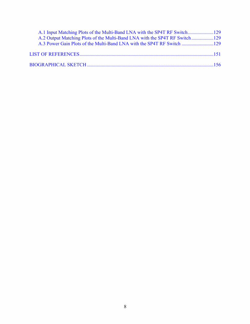
LIST OF TABLES...........................................................................................................................9
LIST OF FIGURES .......................................................................................................................10
ABSTRACT...................................................................................................................................16
CHAPTER
1 INTRODUCTION ..................................................................................................................19
1.1 Motivation and Challenges ...............................................................................................19 1.2 Overview of the Dissertation ............................................................................................20
2 OVERVIEW OF A MULTI-BAND RADIO TRANSCEIVER ............................................22
2.1 Standard Specifications of a Multi-Band Transceiver......................................................22 2.2 Transmitter Architectures .................................................................................................25
2.2.1 Super-Heterodyne Transmitter ...............................................................................25 2.2.2 Direct-Conversion Transmitter...............................................................................26 2.2.3 Offset-PLL Transmitter ..........................................................................................27 2.2.4 Polar Transmitter ....................................................................................................28
2.3 Receiver Architectures......................................................................................................29 2.3.1 Super-Heterodyne Receiver....................................................................................29 2.3.2 Single Conversion Receiver ...................................................................................30
2.4 Proposed Multi-Band Transceiver Architecture ...............................................................32 2.5 Summary...........................................................................................................................35
3 CMOS SINGLE-POLE-FOUR-THROW RF SWITCH ........................................................36
3.1 Introduction.......................................................................................................................36 3.2 Design of the SP4T RF Switch.........................................................................................37 3.3 Implementation of the SP4T RF Switch...........................................................................38 3.4 Measurement Results........................................................................................................40 3.5 Summary...........................................................................................................................45
4 MULTI-BAND LOW NOISE AMPLIFIER WITH THE SP4T RF SWITCH......................46
4.1 Introduction.......................................................................................................................46 4.2 Topologies of Low Noise Amplifiers ...............................................................................48
4.2.1 Common-Source CMOS LNA ...............................................................................48 4.2.2 Proposed Multi-Band Cascode CMOS LNA .........................................................50
4.3 Input Matching of a Multi-Band LNA..............................................................................53
7
4.3.1 Concurrent Dual-Band Cascode CMOS LNA .......................................................53 4.3.2 Input Matching of a Proposed Multi-Band Cascode CMOS LNA.........................54
4.4 Output Matching of the Multi-Band LNA........................................................................59 4.5 Simulation Results of the Multi-Band LNA.....................................................................61 4.6 Single-Pole-Four-Throw RF Switch.................................................................................62
4.6.1 Design and Implementation of SP4T RF Switch ...................................................62 4.6.2 Measurement Results of SP4T RF Switch .............................................................62
4.7 Implementation and Measurement Results of the Multi-Band LNA with the SP4T RF Switch............................................................................................................................65
4.7.1 Input Matching of the Multi-Band LNA with the SP4T RF Switch ......................67 4.7.2 Output Matching of the Multi-Band LNA with SP4T RF Switch..........................70 4.7.3 Power Gain of the Multi-Band LNA with the SP4T RF Switch ............................73 4.7.4 Noise Performance of the Multi-Band LNA with the SP4T RF Switch ................78 4.7.5 Linearity of the Multi-Band LNA with the SP4T RF Switch ................................84
4.8 Summary...........................................................................................................................86
5 Class-F CMOS POWER AMPLIFIER WITH POWER COMBINER ..................................89
5.1 Introduction.......................................................................................................................89 5.2 Power Amplifier Classification ........................................................................................90
5.2.1 Class-A Power Amplifier .......................................................................................90 5.2.2 Class-B Power Amplifier .......................................................................................92 5.2.3 Class-AB and Class-C Power Amplifiers...............................................................94 5.2.4 Class-D Power Amplifier .......................................................................................96 5.2.5 Class-E Power Amplifier........................................................................................96 5.2.6 Class-F Power Amplifier ........................................................................................97
5.3 Design of Class-F Power Amplifier ...............................................................................100 5.3.1 Motivation of Class-F Power Amplifier...............................................................100 5.3.2 Power Combine Topology....................................................................................100 5.3.4 Inverter Driver ......................................................................................................102 5.3.5 Design of 900-MHz CMOS Class-F Power Amplifier ........................................103 5.3.6 Design of Multi-Band CMOS Class-F Power Amplifier .....................................106
5.4 900-MHz Class-F CMOS Power Amplifier Simulations ...............................................108 5.5 Multi-Band Class-F CMOS Power Amplifier Siulations ...............................................113 5.6 Implementation and Measurement Results of the 900-MHz and Multi-Band Class-F
CMOS Power Amplifiers..................................................................................................116 5.7 Summary.........................................................................................................................124
6 SUMMARY AND FUTURE WORK ..................................................................................126
6.1 Summary.........................................................................................................................126 6.2 Future Work....................................................................................................................128
6.2.1 Integrated of the CMOS Multi-Band Receiver ....................................................128 6.2.1 Improvement of 900-MHz and Multi-Band Class-F CMOS Power Amplifiers ..128
APPENDIX: EXPERIMENTAL PLOTS OF THE MULTI-BAND LNA WITH THE SP4T RF SWITCH .........................................................................................................................129
8
A.1 Input Matching Plots of the Multi-Band LNA with the SP4T RF Switch.....................129 A.2 Output Matching Plots of the Multi-Band LNA with the SP4T RF Switch ..................129 A.3 Power Gain Plots of the Multi-Band LNA with the SP4T RF Switch ..........................129
LIST OF REFERENCES.............................................................................................................151
BIOGRAPHICAL SKETCH .......................................................................................................156
9
LIST OF TABLES
Table page 2-1 Specifications for four standards of the multi-band transceiver ........................................22
3-1 Performance of published CMOS RF switches .................................................................44
4-1 The minimum |S11|’s of the multi-band LNA for all four standard frequency bands ........59
4-2 Simulation results of the multi-band LNA.........................................................................62
4-3 Performance of SP4T RF switch........................................................................................64
4-4 Measured return losses (|S11|) of the multi-band LNA with the SP4T RF switch when VDC_d = 0 V, Vdd = 1.2 V, and Ibias = 8 mA........................................................................68
4-5 Measured return losses (|S11|) of the multi-band LNA with the SP4T RF switch when VDC_d = 2 V, Vdd = 1.2 V, and Ibias = 8 mA........................................................................69
4-6 Measured output matching (|S22|) of the multi-band LNA with the SP4T RF switch when VDC_gs = 0 V, Vdd = 1.2 V, and Ibias = 8 mA. ............................................................70
4-7 Measured output matching (|S22|) of the multi-band LNA with the SP4T RF switch when VDC_gs = 0.6 V, Vdd = 1.2 V, and Ibias = 8 mA. .........................................................71
4-8 Measured output matching (|S22|) of the multi-band LNA with the SP4T RF switch when VDC_gs = 1.2 V, Vdd = 1.2 V, and Ibias = 8 mA. .........................................................72
4-9 Measured power gains (|S21|) of the multi-band LNA with the SP4T RF switch..............77
4-10 Performance of published CMOS multi-band or wideband LNA .....................................87
5-1 Maximum output power with ideal single-ended Class-F PA’s ......................................102
5-2 Maximum output power with ideal differential Class-F PA’s.........................................102
5-3 Simulated insertion losses of output power combining transformer for the multi-band Class-F CMOS PA at four frequency bands ....................................................................113
5-4 Performance of published switch type power amplifiers.................................................124
10
LIST OF FIGURES
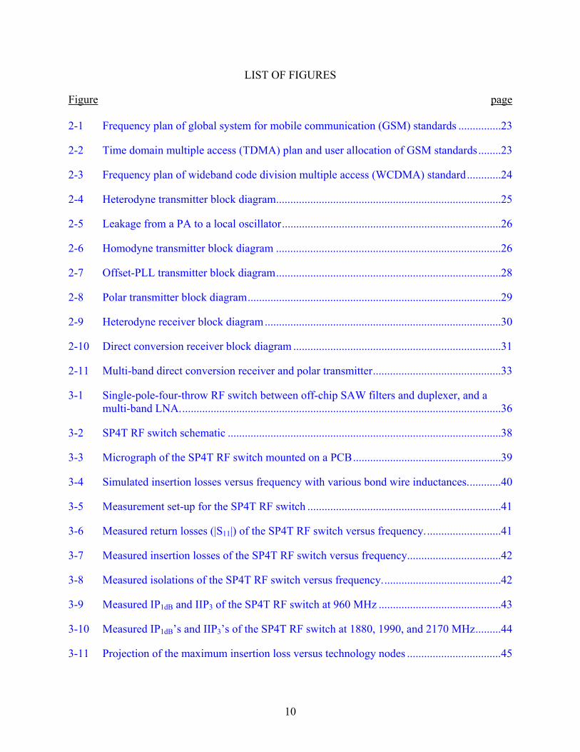
Figure page 2-1 Frequency plan of global system for mobile communication (GSM) standards ...............23
2-2 Time domain multiple access (TDMA) plan and user allocation of GSM standards........23
2-3 Frequency plan of wideband code division multiple access (WCDMA) standard............24
2-4 Heterodyne transmitter block diagram...............................................................................25
2-5 Leakage from a PA to a local oscillator.............................................................................26
2-6 Homodyne transmitter block diagram ...............................................................................26
2-7 Offset-PLL transmitter block diagram...............................................................................28
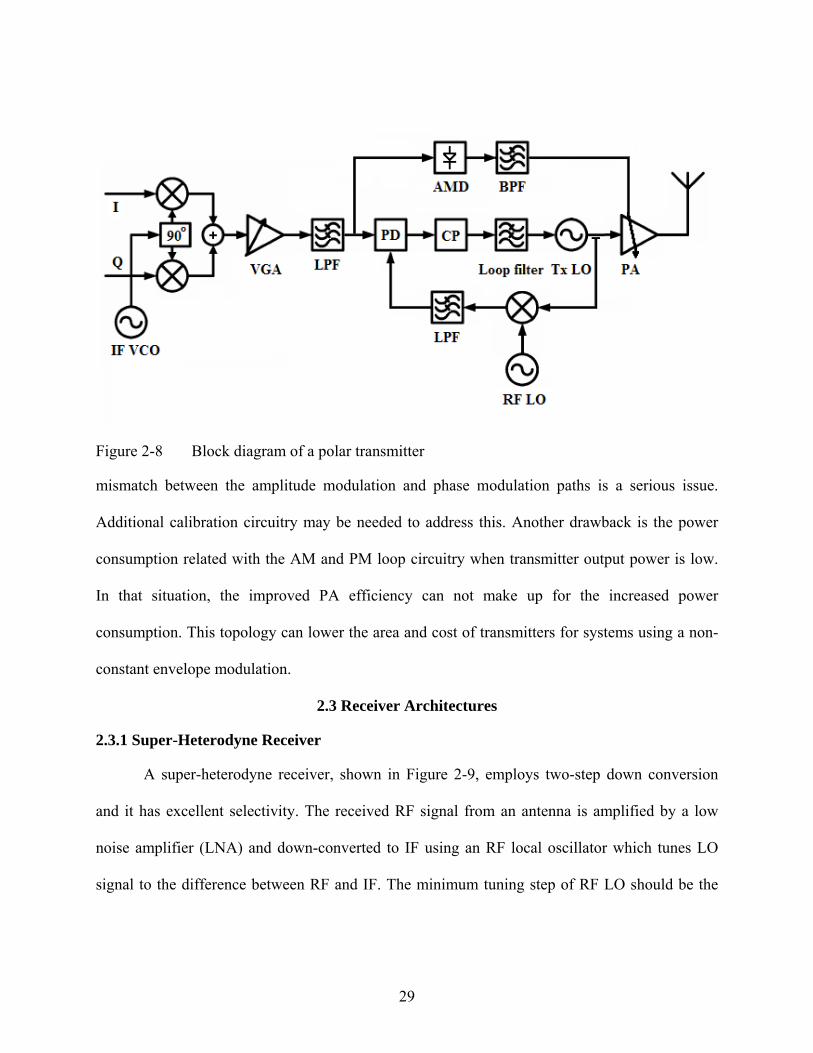
2-8 Polar transmitter block diagram.........................................................................................29
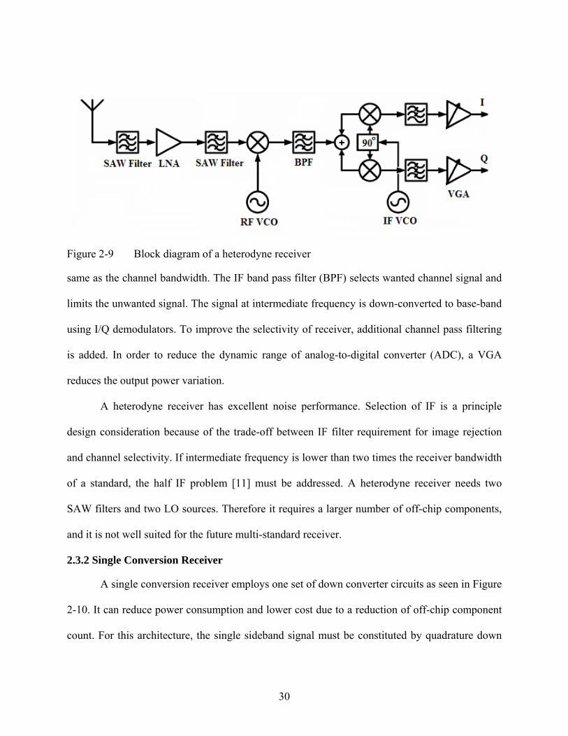
2-9 Heterodyne receiver block diagram...................................................................................30
2-10 Direct conversion receiver block diagram .........................................................................31
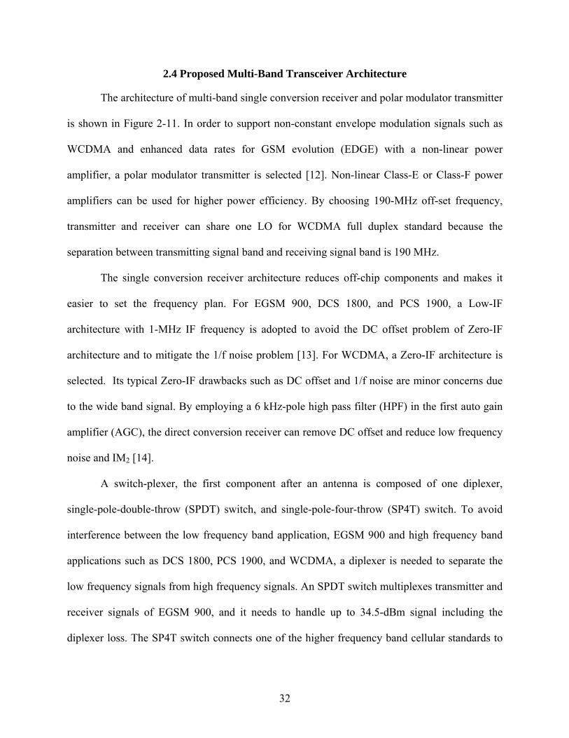
2-11 Multi-band direct conversion receiver and polar transmitter.............................................33
3-1 Single-pole-four-throw RF switch between off-chip SAW filters and duplexer, and a multi-band LNA.................................................................................................................36
3-2 SP4T RF switch schematic ................................................................................................38
3-3 Micrograph of the SP4T RF switch mounted on a PCB....................................................39
3-4 Simulated insertion losses versus frequency with various bond wire inductances............40
3-5 Measurement set-up for the SP4T RF switch ....................................................................41
3-6 Measured return losses (|S11|) of the SP4T RF switch versus frequency...........................41
3-7 Measured insertion losses of the SP4T RF switch versus frequency.................................42
3-8 Measured isolations of the SP4T RF switch versus frequency..........................................42
3-9 Measured IP1dB and IIP3 of the SP4T RF switch at 960 MHz ...........................................43
3-10 Measured IP1dB’s and IIP3’s of the SP4T RF switch at 1880, 1990, and 2170 MHz.........44
3-11 Projection of the maximum insertion loss versus technology nodes .................................45
11
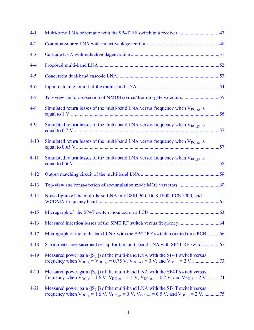
4-1 Multi-band LNA schematic with the SP4T RF switch in a receiver .................................47
4-2 Common-source LNA with inductive degeneration ..........................................................48
4-3 Cascode LNA with inductive degeneration .......................................................................51
4-4 Proposed multi-band LNA.................................................................................................52
4-5 Concurrent dual-band cascode LNA..................................................................................53
4-6 Input matching circuit of the multi-band LNA..................................................................54
4-7 Top-view and cross-section of NMOS source/drain-to-gate varactors..............................55
4-8 Simulated return losses of the multi-band LNA versus frequency when VDC_gs is equal to 1 V........................................................................................................................56
4-9 Simulated return losses of the multi-band LNA versus frequency when VDC_gs is equal to 0.7 V.....................................................................................................................57
4-10 Simulated return losses of the multi-band LNA versus frequency when VDC_gs is equal to 0.65 V...................................................................................................................57
4-11 Simulated return losses of the multi-band LNA versus frequency when VDC_gs is equal to 0.6 V.....................................................................................................................58
4-12 Output matching circuit of the multi-band LNA ...............................................................59
4-13 Top-view and cross-section of accumulation mode MOS varactors .................................60
4-14 Noise figure of the multi-band LNA in EGSM 900, DCS 1800, PCS 1900, and WCDMA frequency bands ................................................................................................61
4-15 Micrograph of the SP4T switch mounted on a PCB.........................................................63
4-16 Measured insertion losses of the SP4T RF switch versus frequency.................................64
4-17 Micrograph of the multi-band LNA with the SP4T RF switch mounted on a PCB ..........66
4-18 S-parameter measurement set-up for the multi-band LNA with SP4T RF switch ............67
4-19 Measured power gain (|S21|) of the multi-band LNA with the SP4T switch versus frequency when VDC_g = VDC_gs = 0.75 V, VDC_out = 0 V, and VDC_d = 2 V. .....................73
4-20 Measured power gain (|S21|) of the multi-band LNA with the SP4T switch versus frequency when VDC_g = 1.6 V, VDC_gs = 1.1 V, VDC_out = 0.2 V, and VDC_d = 2 V. .........74
4-21 Measured power gain (|S21|) of the multi-band LNA with the SP4T switch versus frequency when VDC_g = 1.6 V, VDC_gs = 0 V, VDC_out = 0.5 V, and VDC_d = 2 V. ............75
12
4-22 Measured power gain (|S21|) of the multi-band LNA with the SP4T switch versus frequency when VDC_g = VDC_out = 0.4 V and VDC_gs = VDC_d = 0 V. ................................76
4-23 Simulated power gains of the multi-band LNA with the SP4T RF switch versus frequency with various source degenerative inductances..................................................77
4-24 Noise figure measurement set-up of the multi-band LNA with the SP4T RF switch .......78
4-25 Measured noise figures of the multi-band LNA with the SP4T RF switch from 925 to 960 MHz when VDC_g = VDC_gs = 0.75 V, VDC_out = 0 V, and VDC_d = 2 V. ......................79
4-26 Measured noise figures of the multi-band LNA from 925 to 960 MHz when VDC_g = VDC_gs = 0.75 V, VDC_out = 0 V, and VDC_d = 2 V. .............................................................79
4-27 Measured noise figures of the multi-band LNA with the SP4T switch from 1805 to 1880 MHz when VDC_g = 1.6 V, VDC_gs = 1.1 V, VDC_out = 0.2 V, and VDC_d = 2 V. ........80
4-28 Measured noise figures of the multi-band LNA from 1805 to 1880 MHz when VDC_g = 1.6 V, VDC_gs = 1.1 V, VDC_out = 0.2 V, and VDC_d = 2 V. ..............................................81
4-29 Measured noise figures of the multi-band LNA with the SP4T switch from 1930 to 1990 MHz when VDC_g = 1.6 V, VDC_gs = 0 V, VDC_out = 0.5 V, and VDC_d = 2 V. ...........81
4-30 Measured noise figures of the multi-band LNA from 1930 to 1990 MHz when VDC_g = 1.6 V, VDC_gs = 0 V, VDC_out = 0.5 V, and VDC_d = 2 V. .................................................82
4-31 Measured noise figures of the multi-band LNA with the SP4T switch from 2110 to 2170 MHz when VDC_g = VDC_out = 0.4 V and VDC_gs = VDC_d = 0 V................................83
4-32 Measured noise figures of the multi-band LNA from 2110 to 2170 MHz when VDC_g = VDC_out = 0.4 V and VDC_gs = VDC_d = 0 V. .....................................................................83
4-33 Measured IP1dB and IIP3 of the multi-band LNA with the SP4T RF switch at 930 MHz when VDC_g = VDC_gs = 0.75 V, VDC_out = 0 V, and VDC_d = 2 V. .............................84
4-34 Measured IP1dB and IIP3 of the multi-band LNA with the SP4T RF switch at 1805 MHz when VDC_g = 1.6 V, VDC_gs = 1.1 V, VDC_out = 0.2 V, and VDC_d = 2 V. .................85
4-35 Measured IP1dB and IIP3 of the multi-band LNA with the SP4T RF switch at 1980 MHz when VDC_g = 1.6 V, VDC_gs = 0 V, VDC_out = 0.5 V, and VDC_d = 2 V. ....................85
4-36 Measured IP1dB and IIP3 of the multi-band LNA with the SP4T RF switch at 2110 MHz when VDC_g = VDC_out = 0.4 V and VDC_gs = VDC_d = 0 V..........................................86
5-1 Current source mode PA schematic (Class-A, AB, B, and C)...........................................90
5-2 Input voltage waveform of a Class-A PA..........................................................................91
5-3 Drain voltage and current waveforms of a Class-A PA.....................................................91
13
5-4 Drain voltage and current waveforms of a Class-B PA.....................................................93
5-5 Transformer coupled push-pull PA....................................................................................93
5-6 Drain voltage and current waveforms of Class-AB PA and Class-C PA ..........................95
5-7 Drain voltage and current waveforms of a Class-D PA.....................................................96
5-8 Class-E PA schematic ........................................................................................................96
5-9 Drain voltage and current waveforms of a Class-E PA .....................................................97
5-10 Class-F PA schematic with a λ/4 transmission line...........................................................98
5-11 Drain voltage and current waveform of a Class-F PA with a λ/4 transmission line .........98
5-12 Class-F PA schematic with a third harmonic resonator.....................................................99
5-13 Drain voltage and current waveforms of a Class-F PA with the third harmonic resonator...........................................................................................................................100
5-14 Transformer based power combiner block diagram ........................................................101
5-15 Inverter driver stage shematic..........................................................................................103
5-16 Third harmonic peaking load networks of Class-F PA’s with additional series resonant circuit and parallel resonant circuit ...................................................................104
5-17 Differential 900-MHz Class-F PA with simplified third harmonic peaking circuit and transformer.......................................................................................................................105
5-18 Modified matching capacitor including L1 ......................................................................105
5-19 Tuning schematic of C2 and Cp in the multi-band CMOS Class-F PA............................106
5-20 Inductor tuning schematic using switched resonator concept in the multi-band CMOS Class-F PA...........................................................................................................107
5-21 Load pull simulations of the 900-MHz class-F CMOS PA using advanced design system (ADS)...................................................................................................................108
5-22 Simulated maximum power added efficiency and output power of the Class-F PA versus TI 65-nm NMOS transistor width.........................................................................109
5-23 Layout of output power combining transformer and schematic of individual transformers for the 900-MHz Class-F PA......................................................................110
5-24 Transient output voltage waveform of the 900-MHz Class-F CMOS PA with a power combiner ..........................................................................................................................111
14
5-25 Simulated PAE and output power of the 900-MHz Class-F PA versus supply voltage with 900-MHz input signal ..............................................................................................112
5-26 Output power combining transformer schematic of the multi-band Class-F PA.............113
5-27 Simulated PAE and output power of the multi-band Class-F CMOS PA versus supply voltage at 900 MHz (EGSM 900) ........................................................................114
5-28 Simulated PAE and output power of the multi-band Class-F CMOS PA versus supply voltage at 1750 MHz (DCS 1800)........................................................................115
5-29 Simulated PAE and output power of the multi-band Class-F CMOS PA versus supply voltage at 1880 MHz (PCS 1900) ........................................................................115
5-30 Simulated PAE and output power of the multi-band Class-F CMOS PA versus supply voltage at 1950 MHz (WCDMA).........................................................................116
5-31 Micrograph of the 900-MHz Class-F CMOS PA mounted on a PCB.............................117
5-32 Layer diagram of primary and secondary inductors. .......................................................118
5-33 Micrograph of the multi-band Class-F CMOS PA mounted on a PCB...........................119
5-34 PAE and output power of the 900-MHz Class-F PA versus PA supply voltage. ............120
5-35 Bias current and output power of the 900-MHz Class-F PA versus supply voltage. ......121
5-36 Output power of the 900-Mhz Class-F PA versus frequency. .........................................121
5-37 Supply current of one differential power amplifier versus supply voltage......................122
5-38 Cut and patches using focused ion beam in layout and schematic. .................................123
5-39 Measured drain current of PA versus drain to source voltage. ........................................123
A-1 Measured input matching (|S11|) of the multi-band LNA with SP4T switch versus frequency when VDC_out = VDC_d = 0 V, Vdd = 1.2 V, and Ibias = 8 mA. ..........................130
A-2 Measured input matching (|S11|) of the multi-band LNA with SP4T switch versus frequency when VDC_out = 1 V, VDC_d = 0 V, Vdd = 1.2 V, and Ibias = 8 mA....................131
A-3 Measured input matching (|S11|) of the multi-band LNA with SP4T switch versus frequency when VDC_out = 2 V, VDC_d = 0 V, Vdd = 1.2 V, and Ibias = 8 mA....................132
A-4 Measured input matching (|S11|) of the multi-band LNA with SP4T switch versus frequency when VDC_out = 0 V, VDC_d = 2 V, Vdd = 1.2 V, and Ibias = 8 mA....................133
A-5 Measured input matching (|S11|) of the multi-band LNA with SP4T switch versus frequency when VDC_out = 1 V, VDC_d = 2 V, Vdd = 1.2 V, and Ibias = 8 mA....................134
15
A-6 Measured input matching (|S11|) of the multi-band LNA with SP4T switch versus frequency when VDC_out = VDC_d = 2 V, Vdd = 1.2 V, and Ibias = 8 mA. ..........................135
A-7 Measured output matching (|S22|) of the multi-band LNA with P4T switch versus frequency when VDC_g = VDC_gs = 0 V, Vdd = 1.2 V, and Ibias = 8 mA.............................136
A-8 Measured output matching (|S22|) of the multi-band LNA with SP4T switch versus frequency when VDC_g = 0.8 V, VDC_gs = 0 V, Vdd = 1.2 V, and Ibias = 8 mA..................137
A-9 Measured output matching (|S22|) of the multi-band LNA with SP4T switch versus frequency when VDC_g = 1.6 V, VDC_gs = 0 V, Vdd = 1.2 V, and Ibias = 8 mA..................138
A-10 Measured output matching (|S22|) of the multi-band LNA with SP4T switch versus frequency when VDC_g = 0 V, VDC_gs = 0.6 V, Vdd = 1.2 V, and Ibias = 8 mA..................139
A-11 Measured output matching (|S22|) of the multi-band LNA with SP4T switch versus frequency when VDC_g = 0.8 V, VDC_gs = 0.6 V, Vdd = 1.2 V, and Ibias = 8 mA...............140
A-12 Measured output matching (|S22|) of the multi-band LNA with SP4T switch versus frequency when VDC_g = 1.6 V, VDC_gs = 0.6 V, Vdd = 1.2 V, and Ibias = 8 mA...............141
A-13 Measured output matching (|S22|) of the multi-band LNA with SP4T switch versus frequency when VDC_g = 0 V, VDC_gs = 1.2 V, Vdd = 1.2 V, and Ibias = 8 mA..................142
A-14 Measured output matching (|S22|) of the multi-band LNA with SP4T switch versus frequency when VDC_g = 0.8 V, VDC_gs = 1.2 V, Vdd = 1.2 V, and Ibias = 8 mA...............143
A-15 Measured output matching (|S22|) of the multi-band LNA with SP4T switch versus frequency when VDC_g = 1.6 V, VDC_gs = 1.2 V, Vdd = 1.2 V, and Ibias = 8 mA...............144
A-16 Measured power gain (|S21|) of the multi-band LNA with SP4T switch versus frequency when VDC_out = VDC_d = 0 V, Vdd = 1.2 V, and Ibias = 8 mA. ..........................145
A-17 Measured power gain (|S21|) of the multi-band LNA with SP4T switch versus frequency when VDC_out = 1 V, VDC_d = 0 V, Vdd = 1.2 V, and Ibias = 8 mA....................146
A-18 Measured power gain (|S21|) of the multi-band LNA with SP4T switch versus frequency when VDC_out = 2 V, VDC_d = 0 V, Vdd = 1.2 V, and Ibias = 8 mA....................147
A-19 Measured power gain (|S21|) of the multi-band LNA with SP4T switch versus frequency when VDC_out = 0 V, VDC_d = 2 V, Vdd = 1.2 V, and Ibias = 8 mA....................148
A-20 Measured power gain (|S21|) of the multi-band LNA with P4T switch versus frequency when VDC_out = 1 V, VDC_d = 2 V, Vdd = 1.2 V, and Ibias = 8 mA....................149
A-21 Measured power gain (|S21|) of the multi-band LNA with SP4T switch versus frequency when VDC_out = VDC_d = 2 V, Vdd = 1.2 V, and Ibias = 8 mA. ..........................150

16
Abstract of Dissertation Presented to the Graduate School of the University of Florida in Partial Fulfillment of the Requirements for the Degree of Doctor of Philosophy
COMPLEMENTARY METAL-OXIDE SEMICONDUCTOR RADIO FREQUENCY
INTEGRADED CIRCUIT BLOCKS OF MULTI-BAND TRANSCEIVER FOR COMMUNICATIONS SYSTEMS
By
Kwangchun Jung
December 2008
Chair: Kenneth K. O Major: Electrical and Computer Engineering
The demand for multi-band transceivers that can operate in multiple standards has
increased as communication systems have evolved to the 3rd and 4th generation standards, which
support higher data rate and multiple functions. Several approaches to integrate multiple standard
RF blocks on a single die have been reported. But they simply integrate multiple radios in the
same die. Hence, they occupy a large die area and are high cost.
To implement multi-band radios without excessively increasing die area, hardware must
be shared. A multi-band transceiver should preferably share all active devices except front-end
off-chip components, which means sharing hardware from a low noise amplifier to base-band
circuits in a receiver and from base-band circuits to a power amplifier in a transmitter. To
address this, a multi-band transceiver which consists of a multi-band direct conversion receiver
and a polar transmitter that can support the EGSM 900 (Tx: 880 ~ 915 MHz, Rx: 925 ~ 960
MHz), DCS 1800 (Tx: 1710 ~ 1785 MHz, Rx: 1805 ~ 1880 MHz), PCS 1900 (Tx: 1850 ~ 1910
MHz, Rx: 1930 ~ 1990 MHz), and WCDMA (Tx: 1920 ~ 1980 MHz, Rx: 2110 ~ 2170 MHz)
standards is proposed.
17
The multi-band receiver needs a single-pole-four-throw RF switch which selects one
signal from off-chip SAW filters & duplexer, and passes to a multi-band low noise amplifier
(LNA). An SP4T RF switch has been implemented in a 130-nm CMOS process and has the
maximum insertion loss of 0.49 dB. The input third-order intercept points (IIP3) is 24 dBm for
the EGSM 900 band and 23 dBm for the DCS 1800, PCS 1900, and WCDMA bands. An SP4T
RF switch fabricated in a 90-nm CMOS process has the maximum insertion loss of 0.4 dB. It has
IIP3’s of 24 dBm for the low frequency bands and 23 dBm for the high bands. The insertion loss
can be lower below 0.33 dB using a 65-nm CMOS technology and this should make the
performance degradation due to the switch almost acceptable.
A multi-band low noise amplifier with an SP4T switch has been demonstrated in a UMC
90-nm CMOS process and it can cover the EGSM 900, DCS 1800, PCS 1900, and WCDMA
frequency bands. The multi-band LNA has tunable input and output matching circuits using
variable L-C tanks, and NMOS source/drain to gate and accumulation mode varactors. It has the
maximum noise figures of 1.7, 2.5, 2.5, and 2.6 dB with 9.4-mW power consumption in the
EGSM 900, DCS 1800, PCS 1900, and WCDMA bands, respectively. The maximum power
gains are 19.9, 9.1, 11.5, and 10.1 dB with 9.4-mW power dissipation in the EGSM 900, DCS
1800, PCS 1900, and WCDMA frequency bands, respectively. The IIP3’s are 2.7, 3.2, 3, and 3.3
dBm at 930, 1805, 1980, and 2110 MHz.
Power amplifier implementation using a nano-scale CMOS process is challenging
because the low breakdown voltages of transistors limit the output power. 900-MHz and multi-
band Class-F differential power amplifiers are implemented in a 1.2-V TI 65-nm CMOS process.
The output power limitation can be overcome using a power combining topology which adds the
outputs of 8 differential power amplifiers in series. The multi-band Class-F CMOS PA
18
incorporates tunable harmonic peaking networks using variable capacitors and inductors. The
900-MHz Class-F power amplifier has the simulated maximum power added efficiency of 40.6
% and simulated output power of 2.76 W. The multi-band Class-F PA working in the EGSM 900,
DCS 1800, PCS 1900, and WCDMA bands has simulated output power of 2.8 W with simulated
PAE of 44 % at the EGSM 900 band, and simulated output powers of 2.25~2.35 W with
simulated PAE’s of 44.6 ~ 45.3 % in the DCS 1800, PCS 1900, and WCDMA frequency bands.
The simulations indicate that the multi-band class-F CMOS PA can be used in transmitters for
the EGSM 900, DCS 1800, PCS 1900, and WCDMA frequency standards.
19
CHAPTER 1 INTRODUCTION
1.1 Motivation and Challenges
With the evolution of wireless communication systems to the 3rd and 4th generations, the
necessity for coexistence of different cellular and other wireless systems has increased the
demand for multi-mode, multi-band, multi-standard mobile terminals [1]. Recently, approaches
to implement multi-band systems have been introduced and multi-standard RF blocks are
integrated on a single die [2]-[5]. However, because these IC’s simply incorporate multiple
transceivers, they occupy a large die area, and increase test complexity and cost. To increase
hardware sharing between among radios for varying standards, RF architecture consisting of a
multi-band programmable low noise amplifier (LNA) with a single input and output and a single-
pole-four-throw switch (SP4T) preceding the LNA has been proposed [6], [7]. This multi-band
programmable RF block can support the global system for mobile communication (GSM) such
as extended global system for mobile communication (EGSM 900), digital cellular system (DCS
1800), and personal communication system (PCS 1900), and wide-band code division multiple
access system (WCDMA).
The hardware sharing in a multi-band transceiver is increased by sharing hardware from an
LNA to base-band in a multi-band receiver and from base-band to a power amplifier (PA) in a
multi-band transmitter. To accomplish this, all RF blocks should be tunable. Even if there are a
lot of challenges in both designing the tunable multi-band RF transceiver systems and
implementing each programmable CMOS RF components such as tunable CMOS PA, LNA,
mixers and channel selection filters, this multi-band transceiver should consume reduce cost
resulting from decreased chip area.
20
1.2 Overview of the Dissertation
This research focuses on the design and characterization of key RF circuit blocks in a
multi-band RF transceiver. The goal of this work is to demonstrate SP4T RF switch, multi-band
LNA, and PA with a power combiner in a main stream CMOS technology. The design issues
associated with individual building blocks in the multi-band transceiver will be addressed.
Chapter 2 reviews the RF transmitter and receiver architectures and compares their
advantages and drawbacks. Since WDCMA and GSM including EGSM 900, DCS 1800, and
PCS 1900 are dominant cellular communication systems for the 2nd and 3rd generation
communication standards, the specifications of these four standards and a new multi-band
transceiver block diagram which has a high level of sharing among key components and a
reduced chip area, are described.
An SP4T RF switch is the first on-chip component in the multi-band receiver, and it
needs low insertion loss and moderate linearity & isolation because its insertion loss is directly
added to the overall system noise figure. It selects a signal path among different surface acoustic
wave (SAW) filters and a duplexer. The first SP4T RF switch implemented in 130-nm CMOS
technology is presented in chapter 3.
Chapter 4 presents a multi-band low noise amplifier with an SP4T switch implemented in
a 90-nm CMOS process. The multi-band LNA has tunable input and output matching circuits.
The noise figure and power gain of multi-band LNA are key factors which determine the total
receiver noise performance. The multi-band LAN realizes low noise input matching using bond
wires and off-chip inductors which have high quality factors. The multi-band LNA demonstrates
reasonable noise figures, linearity and gains in EGSM 900, DCS 1800, and PCS 1900, and
WCDMA frequency bands.
21
In chapter 5, 900-MHz and multi-band Class-F differential power amplifiers
implemented in a TI 65-nm CMOS process and the challenges of achieving high output power
and efficiency with low supply voltage and on-chip components are discussed. A power
combining circuit converts differential signals into single ended signals and adds output voltages
in series. The multi-band Class-F PA demonstrates reasonable simulated output powers and
efficiencies in EGSM 900, DCS 1800, PCS 1900, and WCDMA frequency bands.
Finally, the contributions of this research are summarized and suggestions for the future
works are presented in chapter 6.
22
CHAPTER 2 OVERVIEW OF A MULTI-BAND RADIO TRANSCEIVER
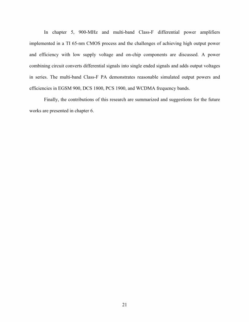
2.1 Standard Specifications of a Multi-Band Transceiver
The global system for mobile communication (GSM) including EGSM 900, DCS 1800,
and PCS 1900 is the most widely used cellular standard in the world and WCDMA is a dominant
communication standard among the 3rd generation standards. Table 2-1 shows the required
specifications for these four standards.
Table 2-1 Specifications for four standards of the multi-band transceiver Standard WCDMA EGSM 900 DCS 1800 PCS 1900
Transmitter Band [MHz] 1920-1980 880-915 1710-1785 1850-1910
Receiver Band [MHz] 2110-2170 925-960 1805-1880 1930-1990
Multiple access CDMA/FDMA TDMA/FDMA TDMA/FDMA TDMA/FDMA
Duplex Method FDD FDD FDD FDD
Channel Spacing 5 MHz 200 KHz 200 KHz 200 KHz
Number of channels
12 (15-50users/ch)
174 (8users/ch)
374 (8users/ch)
299 (8users/ch)
Modulation QPSK GMSK GMSK GMSK
Peak Power [dBm] 24 33 30 30
Sensitivity level [dBm] -117 -102 -102 -102
23
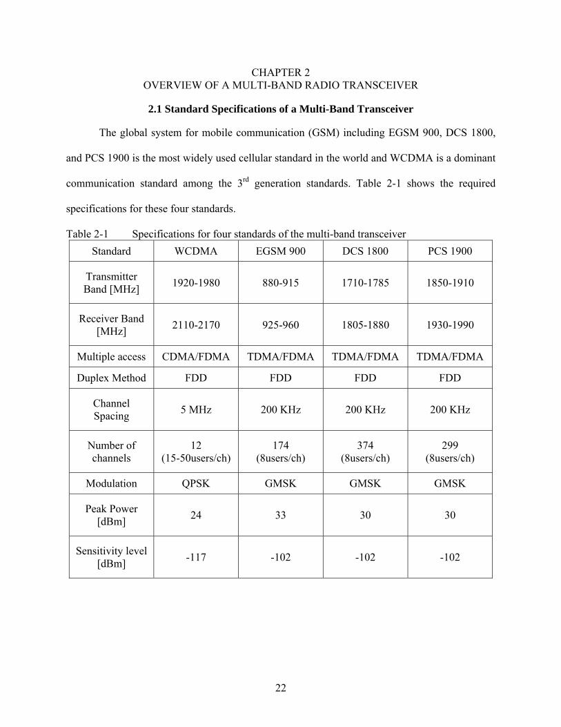
Figure 2-1 Frequency plan of global system for mobile communication (GSM) standards
The GSM standards are defined by European telecommunications standards institute
(ETSI) [8]. These three standards have different carrier frequencies: 880 ~ 915 MHz & 925 ~
960 MHz for EGSM 900 transmitter & receiver, 1710 ~ 1785 MHz & 1805 ~ 1880 MHz for
DCS 1800 transmitter & receiver, and 1850 ~ 1910 MHz & 1930 ~ 1990 MHz for PCS 1900
transmitter & receiver as shown in Figure 2-1.
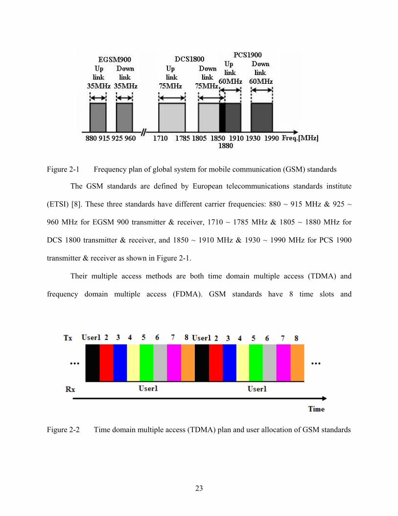
Their multiple access methods are both time domain multiple access (TDMA) and
frequency domain multiple access (FDMA). GSM standards have 8 time slots and
Figure 2-2 Time domain multiple access (TDMA) plan and user allocation of GSM standards
24
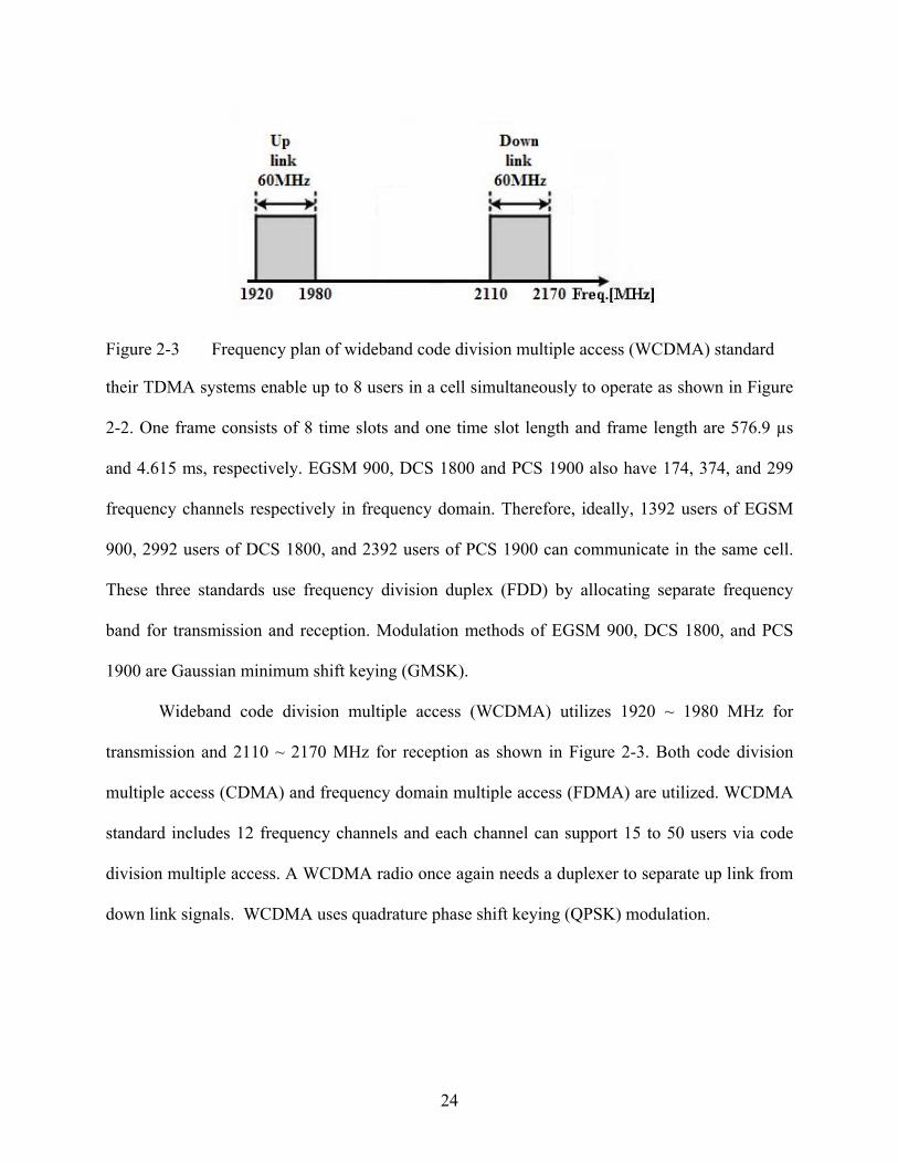
Figure 2-3 Frequency plan of wideband code division multiple access (WCDMA) standard
their TDMA systems enable up to 8 users in a cell simultaneously to operate as shown in Figure
2-2. One frame consists of 8 time slots and one time slot length and frame length are 576.9 µs
and 4.615 ms, respectively. EGSM 900, DCS 1800 and PCS 1900 also have 174, 374, and 299
frequency channels respectively in frequency domain. Therefore, ideally, 1392 users of EGSM
900, 2992 users of DCS 1800, and 2392 users of PCS 1900 can communicate in the same cell.
These three standards use frequency division duplex (FDD) by allocating separate frequency
band for transmission and reception. Modulation methods of EGSM 900, DCS 1800, and PCS
1900 are Gaussian minimum shift keying (GMSK).
Wideband code division multiple access (WCDMA) utilizes 1920 ~ 1980 MHz for
transmission and 2110 ~ 2170 MHz for reception as shown in Figure 2-3. Both code division
multiple access (CDMA) and frequency domain multiple access (FDMA) are utilized. WCDMA
standard includes 12 frequency channels and each channel can support 15 to 50 users via code
division multiple access. A WCDMA radio once again needs a duplexer to separate up link from
down link signals. WCDMA uses quadrature phase shift keying (QPSK) modulation.
25
2.2 Transmitter Architectures
2.2.1 Super-Heterodyne Transmitter
Classic transmitter architecture is the super-heterodyne topology, invented by Edwin H.
Armstrong [9]. Because direct conversion architecture [10] can suffer from the disturbance of an
LO by the PA output leakage, although it has the advantage of simplicity and low cost, super-
heterodyne architecture has been widely utilized. The heterodyne radios have lower power
efficiency, occupy large area and are more costly because they need more on-chip and off-chip
components such as intermediate frequency (IF) & RF filters, 2nd up-conversion mixer and two
local oscillators.
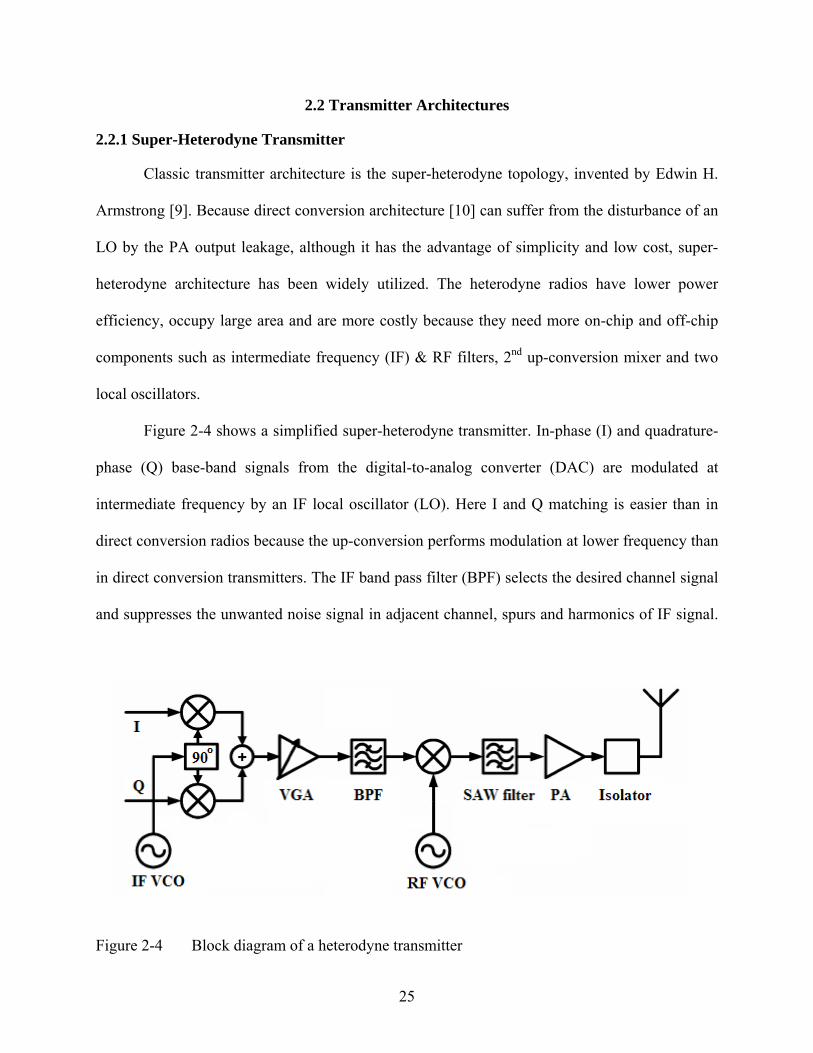
Figure 2-4 shows a simplified super-heterodyne transmitter. In-phase (I) and quadrature-
phase (Q) base-band signals from the digital-to-analog converter (DAC) are modulated at
intermediate frequency by an IF local oscillator (LO). Here I and Q matching is easier than in
direct conversion radios because the up-conversion performs modulation at lower frequency than
in direct conversion transmitters. The IF band pass filter (BPF) selects the desired channel signal
and suppresses the unwanted noise signal in adjacent channel, spurs and harmonics of IF signal.
Figure 2-4 Block diagram of a heterodyne transmitter
26
An RF local oscillator up-converts the signal from IF to carrier frequency and the BPF following
the mixer should have a high Q such as an off-chip SAW filter to limit the unwanted side band
signal produced during 2nd up-conversion mixing. A power amplifier (PA) amplifies the signal
and an isolator protects PA output from reflected signals from an antenna.
2.2.2 Direct-Conversion Transmitter
Direct conversion transmitters are lower cost because they need only one off-chip BPF
and LO. Because of this, direct conversion transmitters are widely utilized. However, designing
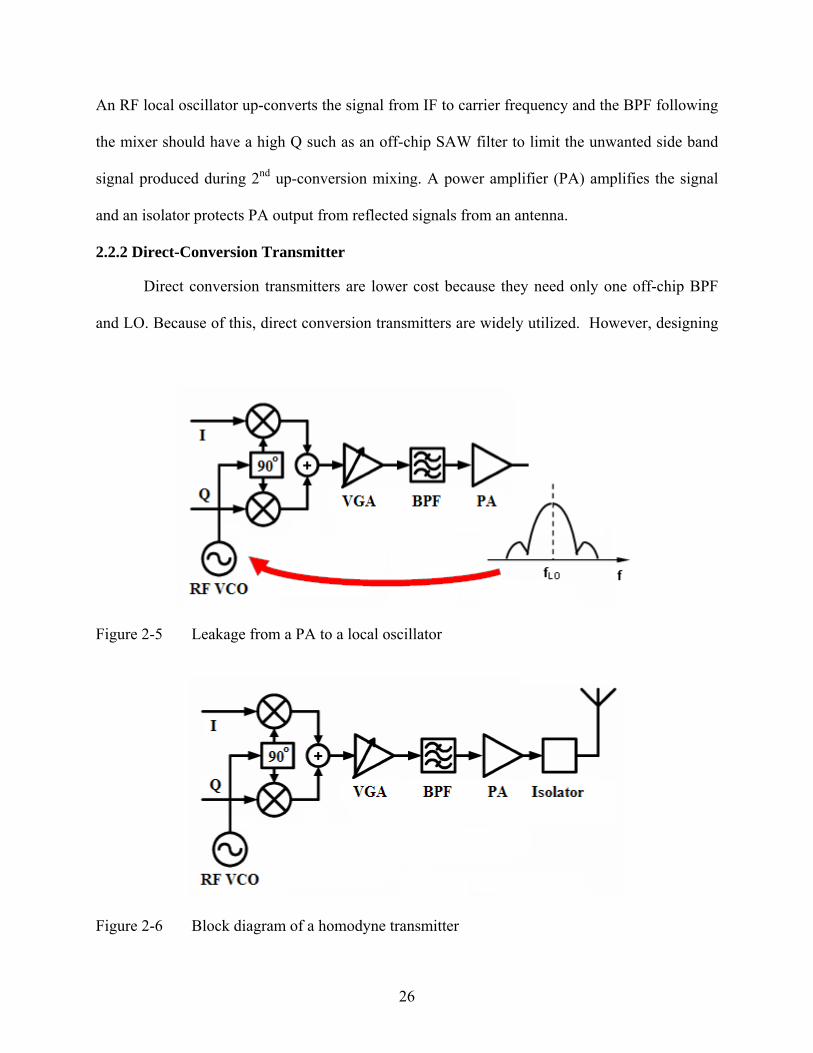
Figure 2-5 Leakage from a PA to a local oscillator
Figure 2-6 Block diagram of a homodyne transmitter
27
on-chip RF components for a direct conversion transmitter is more challenging. The first
challenge is that the PA leakage, shown in Figure 2-5, can corrupt the LO signal of the
transmitter through a mechanism called injection pulling/locking [10]. I/Q mismatch is another
severe problem because direct conversion radios perform modulation at higher carrier frequency.
Figure 2-6 shows a block diagram of a direct conversion transmitter. I and Q signals from
a digital-to-analog converter (DAC) are simultaneously modulated and up-converted to a higher
frequency carrier. The output power of transmitter is controlled by a variable gain amplifier
(VGA). A SAW filter eliminates the unwanted side band signal and a power amplifier amplifies
the signal to a required level. For this topology, channel selection filtering is done in digital or
analog domain using on-chip component instead of employing a high-Q off-chip channel
selection filter as in the heterodyne counterpart. Therefore, the stringent receiver band noise
suppression in GSM standard, less than -162 dBc/Hz at 20-MHz offset, is challenging to satisfy.
2.2.3 Offset-PLL Transmitter
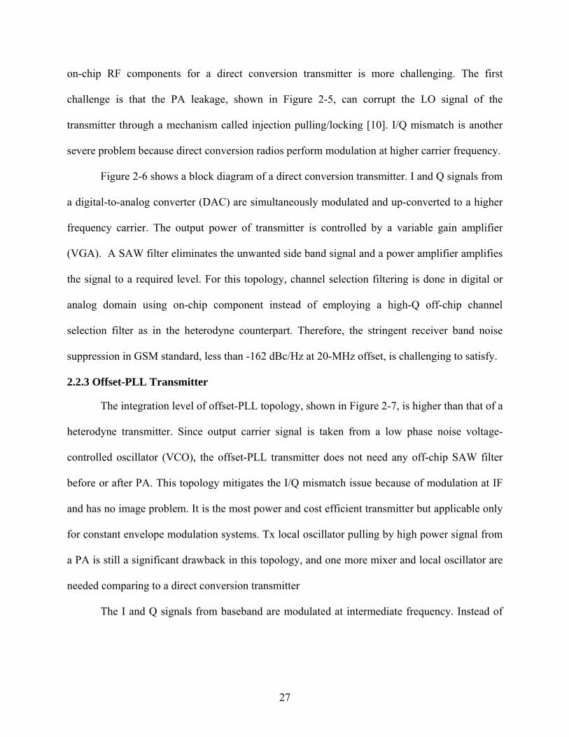
The integration level of offset-PLL topology, shown in Figure 2-7, is higher than that of a
heterodyne transmitter. Since output carrier signal is taken from a low phase noise voltage-
controlled oscillator (VCO), the offset-PLL transmitter does not need any off-chip SAW filter
before or after PA. This topology mitigates the I/Q mismatch issue because of modulation at IF
and has no image problem. It is the most power and cost efficient transmitter but applicable only
for constant envelope modulation systems. Tx local oscillator pulling by high power signal from
a PA is still a significant drawback in this topology, and one more mixer and local oscillator are
needed comparing to a direct conversion transmitter
The I and Q signals from baseband are modulated at intermediate frequency. Instead of
28
Figure 2-7 Block diagram of an offset-PLL transmitter
up-converting to carrier frequency like in a heterodyne transmitter, the phase modulation (PM)
signal is transferred to the Tx VCO through the offset-PLL circuit. The loop filter should be
selected properly to pass phase information while suppressing the out-of-channel noise.
2.2.4 Polar Transmitter
Figure 2-8 shows a polar transmitter and it adds open-loop or closed-loop amplitude
modulation (AM) circuits to the offset-PLL transmitter in order to handle both constant and non-
constant envelope modulations. For non-constant envelope standards, this topology provides a
good power efficient solution using an efficient non-linear power amplifier because the AM loop
circuits compensate for the nonlinearity of PA. The polar transmitter has a high integration level
like the offset-PLL transmitter because PA takes signals from the VCO output which has good
phase noise ant it results in no off-chip filter before and after PA. I/Q mismatch and image
problems are not big issues because the modulation is performed at lower frequency. The delay
29
Figure 2-8 Block diagram of a polar transmitter
mismatch between the amplitude modulation and phase modulation paths is a serious issue.
Additional calibration circuitry may be needed to address this. Another drawback is the power
consumption related with the AM and PM loop circuitry when transmitter output power is low.
In that situation, the improved PA efficiency can not make up for the increased power
consumption. This topology can lower the area and cost of transmitters for systems using a non-
constant envelope modulation.
2.3 Receiver Architectures
2.3.1 Super-Heterodyne Receiver
A super-heterodyne receiver, shown in Figure 2-9, employs two-step down conversion
and it has excellent selectivity. The received RF signal from an antenna is amplified by a low
noise amplifier (LNA) and down-converted to IF using an RF local oscillator which tunes LO
signal to the difference between RF and IF. The minimum tuning step of RF LO should be the
30
Figure 2-9 Block diagram of a heterodyne receiver
same as the channel bandwidth. The IF band pass filter (BPF) selects wanted channel signal and
limits the unwanted signal. The signal at intermediate frequency is down-converted to base-band
using I/Q demodulators. To improve the selectivity of receiver, additional channel pass filtering
is added. In order to reduce the dynamic range of analog-to-digital converter (ADC), a VGA
reduces the output power variation.
A heterodyne receiver has excellent noise performance. Selection of IF is a principle
design consideration because of the trade-off between IF filter requirement for image rejection
and channel selectivity. If intermediate frequency is lower than two times the receiver bandwidth
of a standard, the half IF problem [11] must be addressed. A heterodyne receiver needs two
SAW filters and two LO sources. Therefore it requires a larger number of off-chip components,
and it is not well suited for the future multi-standard receiver.
2.3.2 Single Conversion Receiver
A single conversion receiver employs one set of down converter circuits as seen in Figure
2-10. It can reduce power consumption and lower cost due to a reduction of off-chip component
count. For this architecture, the single sideband signal must be constituted by quadrature down
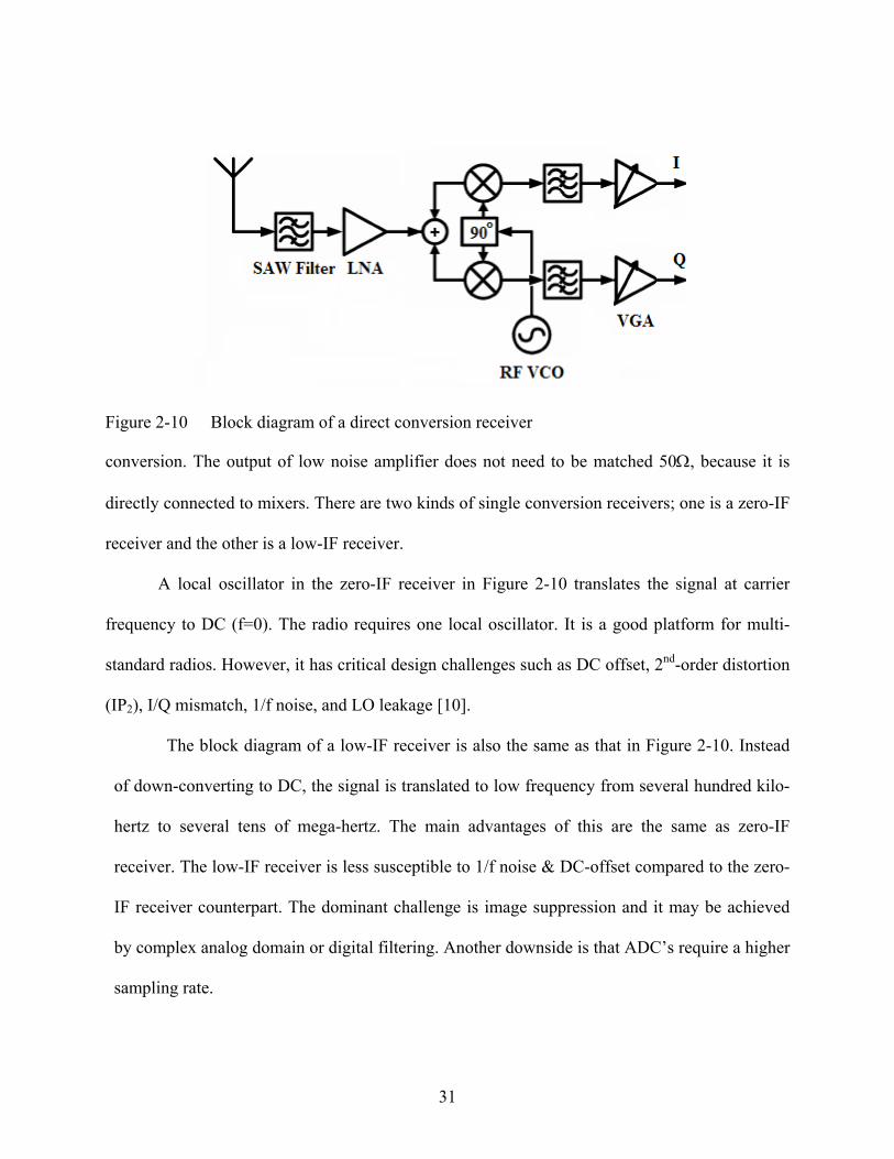
31
Figure 2-10 Block diagram of a direct conversion receiver
conversion. The output of low noise amplifier does not need to be matched 50Ω, because it is
directly connected to mixers. There are two kinds of single conversion receivers; one is a zero-IF
receiver and the other is a low-IF receiver.
A local oscillator in the zero-IF receiver in Figure 2-10 translates the signal at carrier
frequency to DC (f=0). The radio requires one local oscillator. It is a good platform for multi-
standard radios. However, it has critical design challenges such as DC offset, 2nd-order distortion
(IP2), I/Q mismatch, 1/f noise, and LO leakage [10].
The block diagram of a low-IF receiver is also the same as that in Figure 2-10. Instead
of down-converting to DC, the signal is translated to low frequency from several hundred kilo-
hertz to several tens of mega-hertz. The main advantages of this are the same as zero-IF
receiver. The low-IF receiver is less susceptible to 1/f noise & DC-offset compared to the zero-
IF receiver counterpart. The dominant challenge is image suppression and it may be achieved
by complex analog domain or digital filtering. Another downside is that ADC’s require a higher
sampling rate.
32
2.4 Proposed Multi-Band Transceiver Architecture
The architecture of multi-band single conversion receiver and polar modulator transmitter
is shown in Figure 2-11. In order to support non-constant envelope modulation signals such as
WCDMA and enhanced data rates for GSM evolution (EDGE) with a non-linear power
amplifier, a polar modulator transmitter is selected [12]. Non-linear Class-E or Class-F power
amplifiers can be used for higher power efficiency. By choosing 190-MHz off-set frequency,
transmitter and receiver can share one LO for WCDMA full duplex standard because the
separation between transmitting signal band and receiving signal band is 190 MHz.
The single conversion receiver architecture reduces off-chip components and makes it
easier to set the frequency plan. For EGSM 900, DCS 1800, and PCS 1900, a Low-IF
architecture with 1-MHz IF frequency is adopted to avoid the DC offset problem of Zero-IF
architecture and to mitigate the 1/f noise problem [13]. For WCDMA, a Zero-IF architecture is
selected. Its typical Zero-IF drawbacks such as DC offset and 1/f noise are minor concerns due
to the wide band signal. By employing a 6 kHz-pole high pass filter (HPF) in the first auto gain
amplifier (AGC), the direct conversion receiver can remove DC offset and reduce low frequency
noise and IM2 [14].
A switch-plexer, the first component after an antenna is composed of one diplexer,
single-pole-double-throw (SPDT) switch, and single-pole-four-throw (SP4T) switch. To avoid
interference between the low frequency band application, EGSM 900 and high frequency band
applications such as DCS 1800, PCS 1900, and WCDMA, a diplexer is needed to separate the
low frequency signals from high frequency signals. An SPDT switch multiplexes transmitter and
receiver signals of EGSM 900, and it needs to handle up to 34.5-dBm signal including the
diplexer loss. The SP4T switch connects one of the higher frequency band cellular standards to
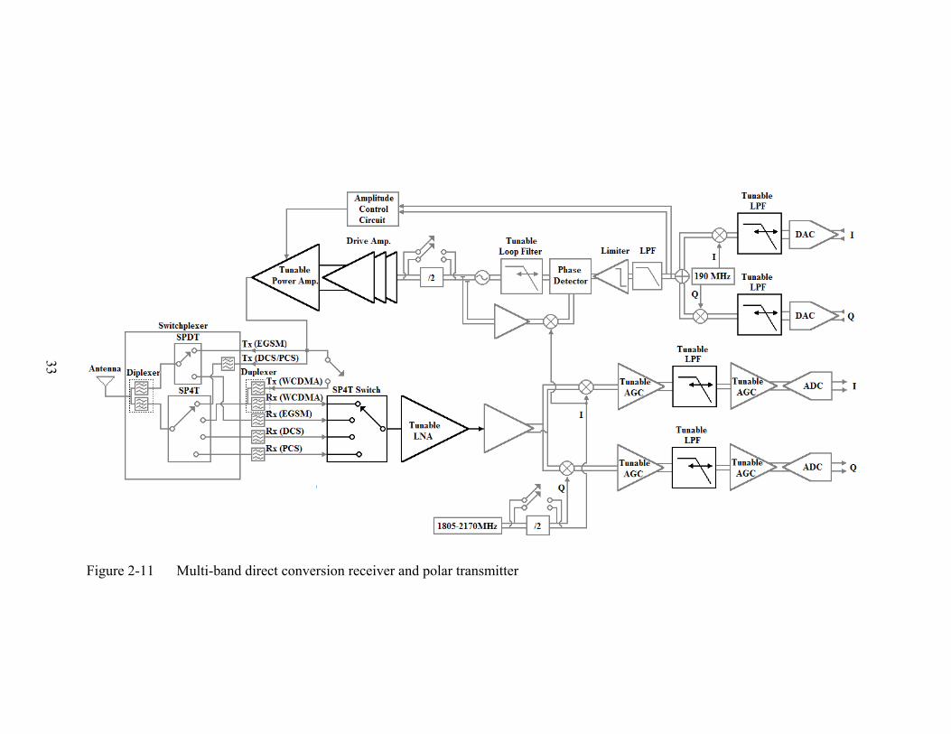
33
Figure 2-11 Multi-band direct conversion receiver and polar transmitter
34
an antenna. Its required linearity is mainly determined by WCDMA transmitter signals and it has
to handle up to 26 dBm.
The duplexer separates WCDMA transmitter and receiver signals. The receiver
specifications such as IIP2 and IIP3 strongly depend on the duplexer TX-RX isolation. An
insertion loss of duplexer is also important because it directly adds receiver noise figure. A
Murata duplexer with 1.8-dB IL and 54-dB isolation [15] is pretty reasonable choice for this
application.
The SP4T RF switch consists of the four transistors and four gate resistors, and performs
the switching function to select signals from SAW filter banks or a duplexer to a multi-band low
noise amplifier input. Since the SP4T RF switch handles only received signals, it does not need
to handle large power like a T/R switch. Insertion loss of the SP4T RF switch increases receiver
noise figure, so reducing insertion loss is the most important issue for the SP4T RF switch
design.
The output of SP4T RF switch is amplified by a multi-band low noise amplifier. LNA
gain and noise figure are critical design specifications for the receiver noise figure. Sufficient
performance should be attained without using an excessive number of off-chip components.
CMOS power amplifiers have two important design challenges; one is achieving
sufficient output power and efficiency with on-chip components in deep sub-micron CMOS
technology and the other is incorporating tuning capability to support the four different
frequency bands. EGSM 900 needs 33-dBm output power at antenna port and a PA needs around
34.5-dBm output power considering front end losses between an antenna and a PA.
Unfortunately, the supply voltage of deep sub-micron CMOS has been decreased down to 1 V.
Since the output power is proportion to the square of supply voltage and inversely proportional
35
to the load impedance, this makes the PA design especially challenging. The selection of load
impedance must be optimized and the outputs must be combined to achieve sufficient power.
2.5 Summary
This chapter presented a brief overview of EGSM 900, DCS 1800, PCS 1900, and
WCDMA standard specifications, and reviewed possible transmitter and receiver architectures.
The proposed multi-band transceiver can reduce power consumption by a using a high efficiency
multi-band power amplifier, and lower cost and area by increasing hardware sharing. The
implementation and analyses of key components of the multi-band transceiver will be discussed
in the following chapters.
36
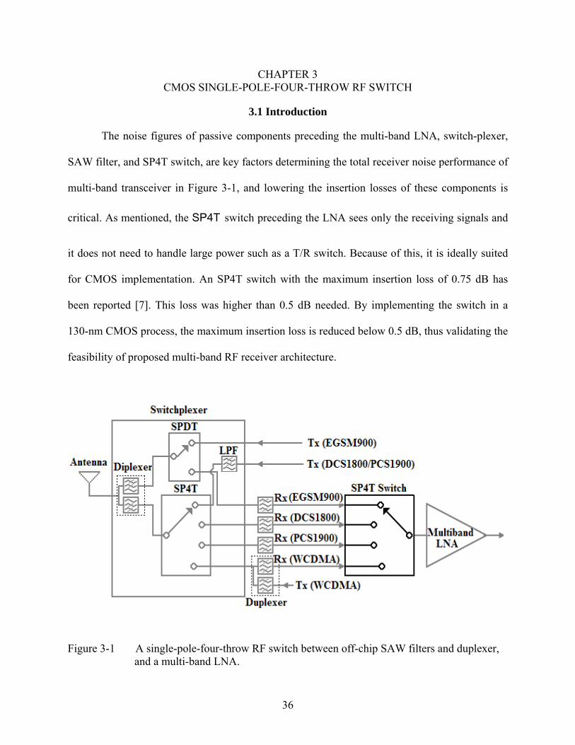
CHAPTER 3 CMOS SINGLE-POLE-FOUR-THROW RF SWITCH
3.1 Introduction
The noise figures of passive components preceding the multi-band LNA, switch-plexer,
SAW filter, and SP4T switch, are key factors determining the total receiver noise performance of
multi-band transceiver in Figure 3-1, and lowering the insertion losses of these components is
critical. As mentioned, the SP4T switch preceding the LNA sees only the receiving signals and
it does not need to handle large power such as a T/R switch. Because of this, it is ideally suited
for CMOS implementation. An SP4T switch with the maximum insertion loss of 0.75 dB has
been reported [7]. This loss was higher than 0.5 dB needed. By implementing the switch in a
130-nm CMOS process, the maximum insertion loss is reduced below 0.5 dB, thus validating the
feasibility of proposed multi-band RF receiver architecture.
Figure 3-1 A single-pole-four-throw RF switch between off-chip SAW filters and duplexer,
and a multi-band LNA.
37
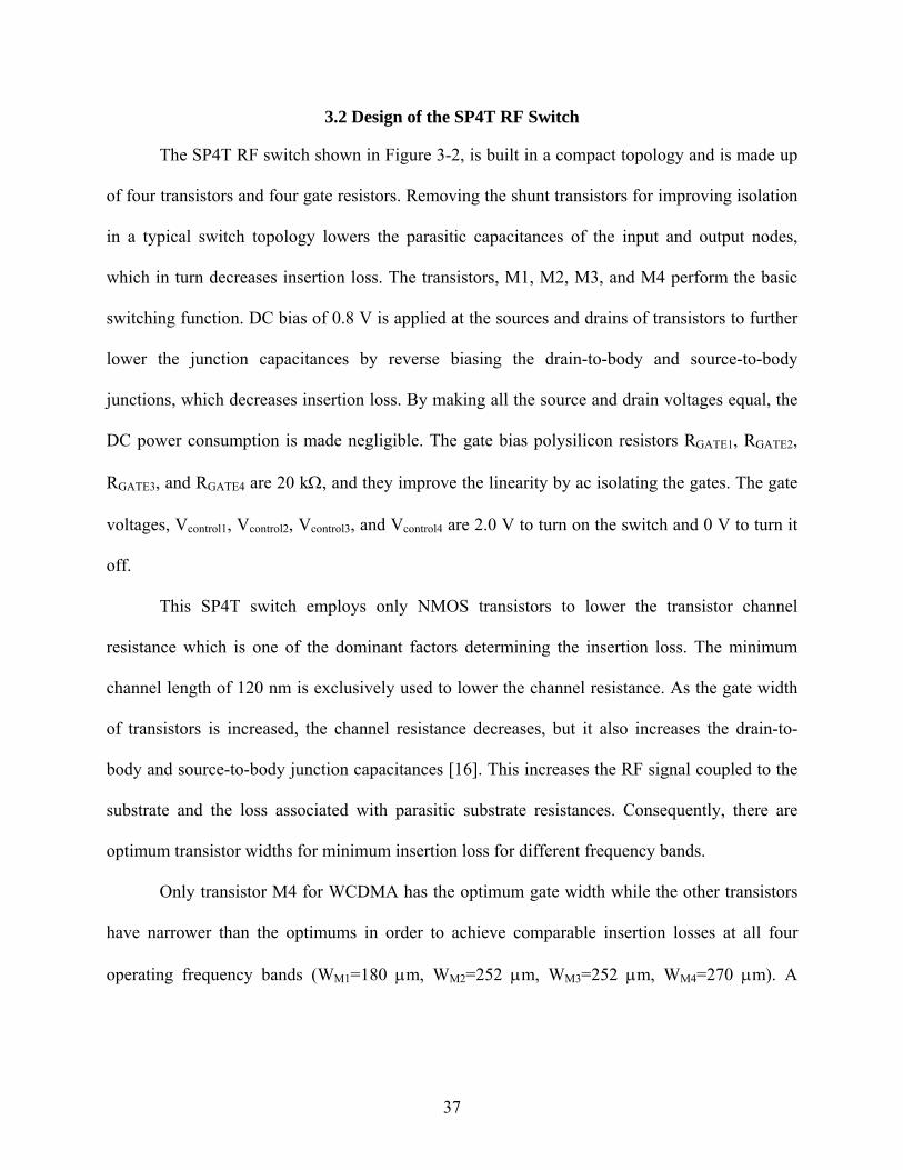
3.2 Design of the SP4T RF Switch
The SP4T RF switch shown in Figure 3-2, is built in a compact topology and is made up
of four transistors and four gate resistors. Removing the shunt transistors for improving isolation
in a typical switch topology lowers the parasitic capacitances of the input and output nodes,
which in turn decreases insertion loss. The transistors, M1, M2, M3, and M4 perform the basic
switching function. DC bias of 0.8 V is applied at the sources and drains of transistors to further
lower the junction capacitances by reverse biasing the drain-to-body and source-to-body
junctions, which decreases insertion loss. By making all the source and drain voltages equal, the
DC power consumption is made negligible. The gate bias polysilicon resistors RGATE1, RGATE2,
RGATE3, and RGATE4 are 20 kΩ, and they improve the linearity by ac isolating the gates. The gate
voltages, Vcontrol1, Vcontrol2, Vcontrol3, and Vcontrol4 are 2.0 V to turn on the switch and 0 V to turn it
off.
This SP4T switch employs only NMOS transistors to lower the transistor channel
resistance which is one of the dominant factors determining the insertion loss. The minimum
channel length of 120 nm is exclusively used to lower the channel resistance. As the gate width
of transistors is increased, the channel resistance decreases, but it also increases the drain-to-
body and source-to-body junction capacitances [16]. This increases the RF signal coupled to the
substrate and the loss associated with parasitic substrate resistances. Consequently, there are
optimum transistor widths for minimum insertion loss for different frequency bands.
Only transistor M4 for WCDMA has the optimum gate width while the other transistors
have narrower than the optimums in order to achieve comparable insertion losses at all four
operating frequency bands (WM1=180 μm, WM2=252 μm, WM3=252 μm, WM4=270 μm). A
38
Figure 3-2 Schematic of the SP4T RF switch
multi-finger interdigitated transistor layout [16] is used to reduce the drain and source junction
capacitances.
3.3 Implementation of the SP4T RF Switch
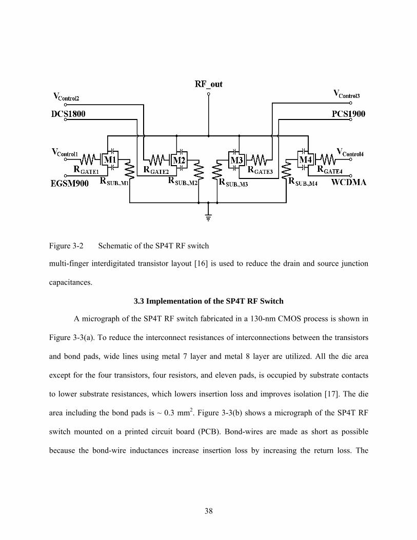
A micrograph of the SP4T RF switch fabricated in a 130-nm CMOS process is shown in
Figure 3-3(a). To reduce the interconnect resistances of interconnections between the transistors
and bond pads, wide lines using metal 7 layer and metal 8 layer are utilized. All the die area
except for the four transistors, four resistors, and eleven pads, is occupied by substrate contacts
to lower substrate resistances, which lowers insertion loss and improves isolation [17]. The die
area including the bond pads is ~ 0.3 mm2. Figure 3-3(b) shows a micrograph of the SP4T RF
switch mounted on a printed circuit board (PCB). Bond-wires are made as short as possible
because the bond-wire inductances increase insertion loss by increasing the return loss. The
39
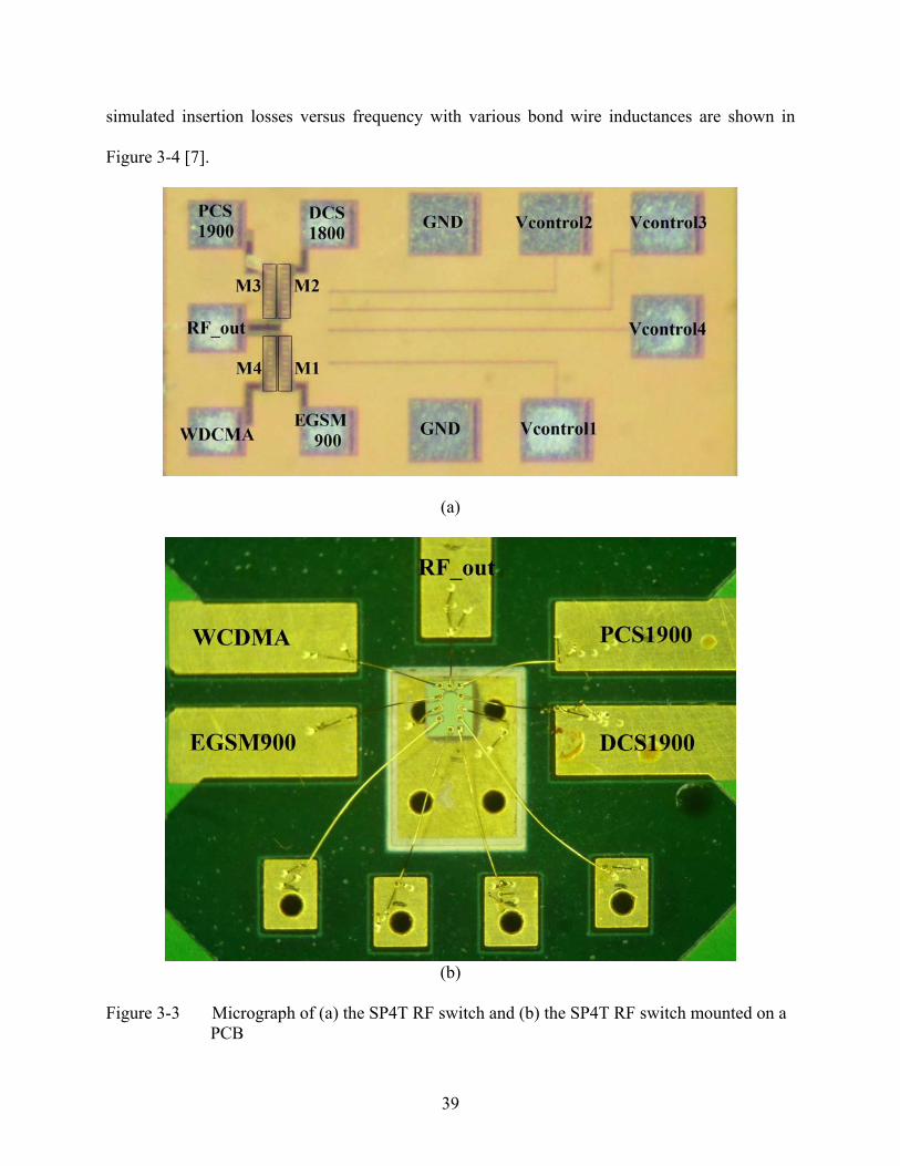
simulated insertion losses versus frequency with various bond wire inductances are shown in
Figure 3-4 [7].
(a)
(b)
Figure 3-3 Micrograph of (a) the SP4T RF switch and (b) the SP4T RF switch mounted on a
PCB
40
Figure 3-4 Simulated insertion losses versus frequency with various bond wire inductances.
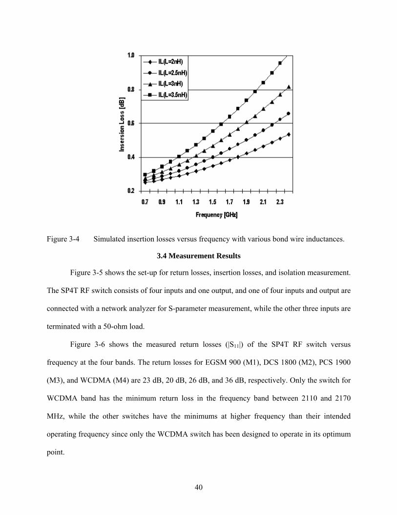
3.4 Measurement Results
Figure 3-5 shows the set-up for return losses, insertion losses, and isolation measurement.
The SP4T RF switch consists of four inputs and one output, and one of four inputs and output are
connected with a network analyzer for S-parameter measurement, while the other three inputs are
terminated with a 50-ohm load.
Figure 3-6 shows the measured return losses (|S11|) of the SP4T RF switch versus
frequency at the four bands. The return losses for EGSM 900 (M1), DCS 1800 (M2), PCS 1900
(M3), and WCDMA (M4) are 23 dB, 20 dB, 26 dB, and 36 dB, respectively. Only the switch for
WCDMA band has the minimum return loss in the frequency band between 2110 and 2170
MHz, while the other switches have the minimums at higher frequency than their intended
operating frequency since only the WCDMA switch has been designed to operate in its optimum
point.
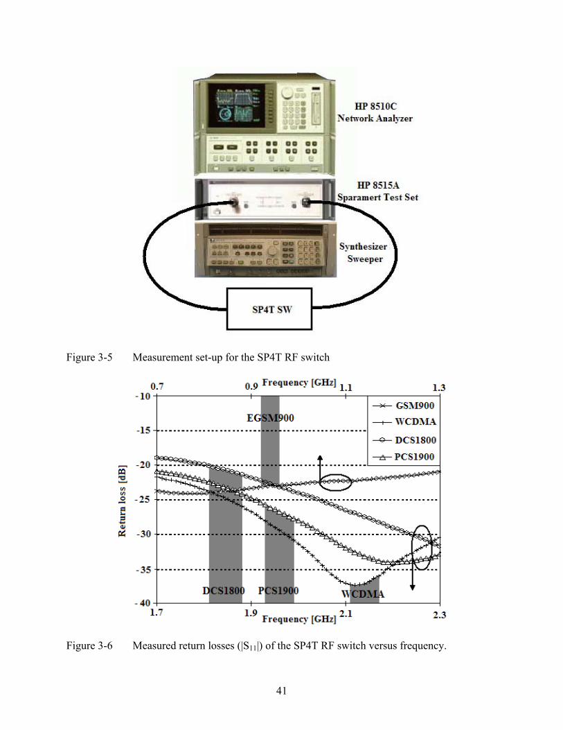
41
Figure 3-5 Measurement set-up for the SP4T RF switch
Figure 3-6 Measured return losses (|S11|) of the SP4T RF switch versus frequency.
42
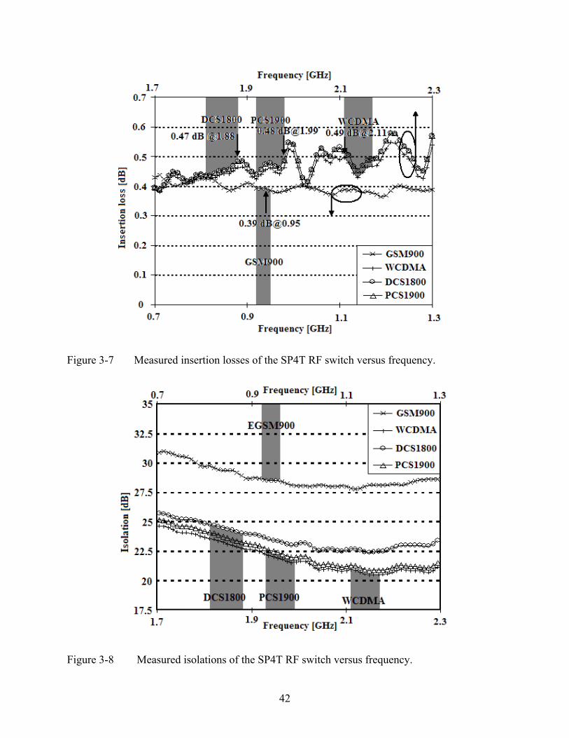
Figure 3-7 Measured insertion losses of the SP4T RF switch versus frequency.
Figure 3-8 Measured isolations of the SP4T RF switch versus frequency.
43
Figure 3-7 shows the measured insertion losses of the SP4T RF switch versus frequency.
The insertion losses in EGSM 900, DCS 1800, PCS 1900 and WCDMA are 0.39 dB at 960
MHz, 0.47 dB at 1880 MHz, 0.48 dB at 1990 MHz, and 0.49 dB at 2110 MHz, respectively,
which are excellent.
The isolation performances of the SP4T RF switch versus frequency are shown in Figure
3-8 and EGSM 900, DCS 1800, PCS 1900, and WCDMA have isolations of 28 dB, 24 dB, 22
dB, and 21 dB, respectively. The total isolation of the multi-band transceiver in Figure 3-1 is the
sum of SP4T switch isolation and that of switch-plexer [18]. Hence, the total isolation will be
larger than 47 dB.
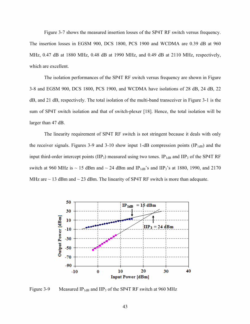
The linearity requirement of SP4T RF switch is not stringent because it deals with only
the receiver signals. Figures 3-9 and 3-10 show input 1-dB compression points (IP1dB) and the
input third-order intercept points (IIP3) measured using two tones. IP1dB and IIP3 of the SP4T RF
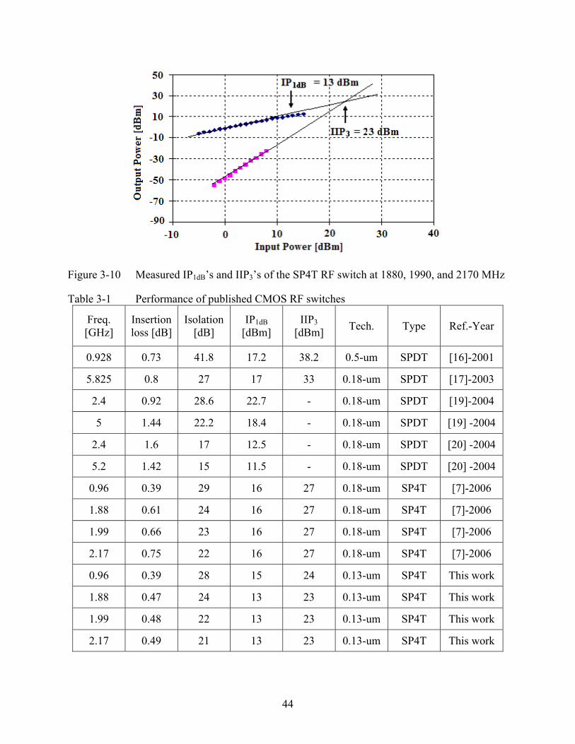
switch at 960 MHz is ~ 15 dBm and ~ 24 dBm and IP1dB’s and IIP3’s at 1880, 1990, and 2170
MHz are ~ 13 dBm and ~ 23 dBm. The linearity of SP4T RF switch is more than adequate.
Figure 3-9 Measured IP1dB and IIP3 of the SP4T RF switch at 960 MHz
44
Figure 3-10 Measured IP1dB’s and IIP3’s of the SP4T RF switch at 1880, 1990, and 2170 MHz
Table 3-1 Performance of published CMOS RF switches
Freq. [GHz]
Insertion loss [dB]
Isolation [dB]
IP1dB [dBm]
IIP3 [dBm]
Tech. Type Ref.-Year
0.928 0.73 41.8 17.2 38.2 0.5-um SPDT [16]-2001
5.825 0.8 27 17 33 0.18-um SPDT [17]-2003
2.4 0.92 28.6 22.7 - 0.18-um SPDT [19]-2004
5 1.44 22.2 18.4 - 0.18-um SPDT [19] -2004
2.4 1.6 17 12.5 - 0.18-um SPDT [20] -2004
5.2 1.42 15 11.5 - 0.18-um SPDT [20] -2004
0.96 0.39 29 16 27 0.18-um SP4T [7]-2006
1.88 0.61 24 16 27 0.18-um SP4T [7]-2006
1.99 0.66 23 16 27 0.18-um SP4T [7]-2006
2.17 0.75 22 16 27 0.18-um SP4T [7]-2006
0.96 0.39 28 15 24 0.13-um SP4T This work
1.88 0.47 24 13 23 0.13-um SP4T This work
1.99 0.48 22 13 23 0.13-um SP4T This work
2.17 0.49 21 13 23 0.13-um SP4T This work
45
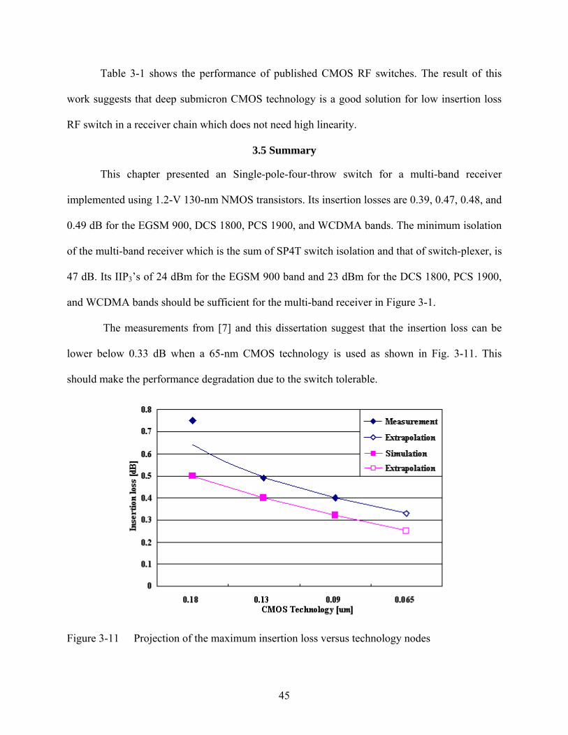
Table 3-1 shows the performance of published CMOS RF switches. The result of this
work suggests that deep submicron CMOS technology is a good solution for low insertion loss
RF switch in a receiver chain which does not need high linearity.
3.5 Summary
This chapter presented an Single-pole-four-throw switch for a multi-band receiver
implemented using 1.2-V 130-nm NMOS transistors. Its insertion losses are 0.39, 0.47, 0.48, and
0.49 dB for the EGSM 900, DCS 1800, PCS 1900, and WCDMA bands. The minimum isolation
of the multi-band receiver which is the sum of SP4T switch isolation and that of switch-plexer, is
47 dB. Its IIP3’s of 24 dBm for the EGSM 900 band and 23 dBm for the DCS 1800, PCS 1900,
and WCDMA bands should be sufficient for the multi-band receiver in Figure 3-1.
The measurements from [7] and this dissertation suggest that the insertion loss can be
lower below 0.33 dB when a 65-nm CMOS technology is used as shown in Fig. 3-11. This
should make the performance degradation due to the switch tolerable.
Figure 3-11 Projection of the maximum insertion loss versus technology nodes
46
CHAPTER 4 MULTI-BAND LOW NOISE AMPLIFIER WITH THE SP4T RF SWITCH
4.1 Introduction
Wide-band code division multiple access system (WCDMA) has -117-dBm receiver
sensitivity [21] and the global system for mobile communication (GSM) including EGSM900,
DCS1800, and PCS1900 has -102-dBm sensitivity [8]. This means a receiver for these standards
has to detect very weak signal without adding much noise. Because of this, a low noise amplifier
(LNA) is particularly a key building block in a receiver.
The noise factor of a system is output and input S/N ratios and in a cascade system, the
total noise factor (F) [22] of n stages,
12121
3
1
21
111
−⋅⋅⋅−
+⋅⋅⋅+−
+−
+==n
n
outout
inin
GGGF
GGF
GFF
NSNSF , (4-1)
where, inin NS and outout NS are the input and output signal-to-noise ratios, 1F is the noise
factor of the first stage, iF is the noise factor of i-th stage, 1G is the power gain of the first
stage and iG is the power gain of i-th stage. The receiver noise performance is characterized by
noise figure (NF), which is the equivalent quantity in decibels of the noise factor (F).
)log(10 FNF = . (4-2)
Equation (4-1) shows the noise factors of later stages are divided by the gains of preceding stages.
Hence, the overall receiver noise factor is dominated by the first few stages including the first
gain stage. The first gain block should have a low noise factor. Figure 2-1 shows the schematic
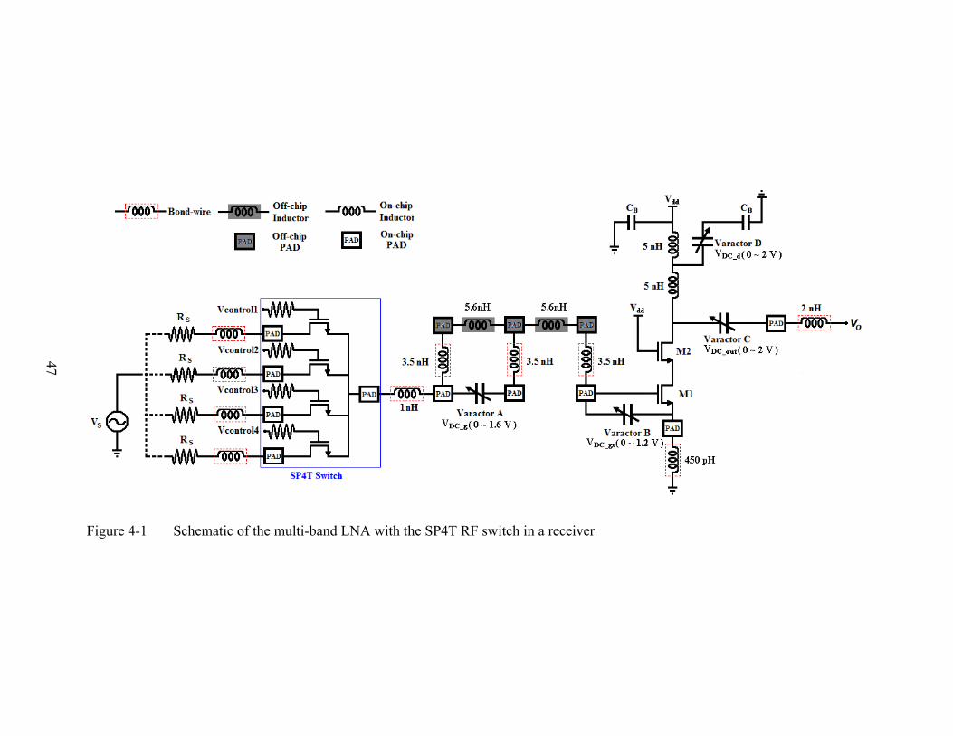
of multi-band LNA with an SP4T RF switch in a receiver. This circuit is designed and
implemented in the UMC 90-nm logic CMOS process.
47
Figure 4-1 Schematic of the multi-band LNA with the SP4T RF switch in a receiver
48
4.2 Topologies of Low Noise Amplifiers
4.2.1 Common-Source CMOS LNA
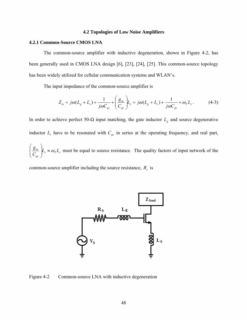
The common-source amplifier with inductive degeneration, shown in Figure 4-2, has
been generally used in CMOS LNA design [6], [23], [24], [25]. This common-source topology
has been widely utilized for cellular communication systems and WLAN’s.
The input impedance of the common-source amplifier is
sTgs
sgsgs
m
gssgin L
CjLLjL
Cg
CjLLjZ ω
ωω
ωω +++=⎟
⎟⎠
⎞⎜⎜⎝
⎛+++=
1)(1)( . (4-3)
In order to achieve perfect 50-Ω input matching, the gate inductor gL and source degenerative
inductor sL have to be resonated with gsC in series at the operating frequency, and real part,
sTsgs
m LLCg ω≈⎟
⎟⎠
⎞⎜⎜⎝
⎛ must be equal to source resistance. The quality factors of input network of the
common-source amplifier including the source resistance, sR is
Figure 4-2 Common-source LNA with inductive degeneration
49
sgssTsgs RCLRCQ
00 21
)(1
ωωω≈
+= . (4-4)
The effective transconductance of common-source LNA at resonance is
)1()(0
0
s
sTs
T
sTsgs
mmm
RLRLRC
gQgG ωω
ωωω +
=+
== , (4-5)
when the input impedance is perfectly matched, sin RZ = ,
)(21
0ωωT
sm R
G = . (4-6)
The Multi-band operation frequencies are much less than Tω , and the value of 0ω
ωT is much
larger than 1. Therefore, the common-source topology has higher gain than the conventional
common-gate topology )21(
sm R
G = . However, the common-gate topology has better linearity
than the common-source topology.
In MOSFET’s, there are two major sources of noise: flicker noise and thermal noise.
Since RF amplifiers operate at high frequencies, the channel thermal noise is dominant. Thermal
noise is generated by random thermal motion of channel carriers. The power spectral density of
the drain thermal noise [26] is
dod gkTHzAf
iγ4]/[ 2
2
=Δ
. (4-7)
where k is the Boltzmann’s constant (=1.38 ×10⁻²³ J/K), T is an absolute temperature, γ is 2/3 for
long channel devices, and gdo is the short-circuit drain conductance of transistor.
50
At high frequencies, the voltage fluctuation in the channel couples to the gate through the
oxide capacitance, resulting in the gate noise current. The spectral density of gate induced noise
[26] is
do
gsg
gC
kTf
i5
4222 ω
δ=Δ
, (4-8)
where δ is the gate noise coefficient and 4/3 for long channel devices. Since the channel noise
and induced gate noise are physically generated by the same noise source, they are correlated.
The correlation coefficient is
395.0325
22
*
jjii
iic
dg
dg −=−=⋅
⋅= (4-9)
For CS-LNA, assuming a 1-Hz bandwidth and including the drain thermal noise, gate inductor
resistance Rl, and the gate resistance of the NMOS device Rg, noise factor is
201 ⎟⎟⎠
⎞⎜⎜⎝
⎛+++=
Tsdo
s
g
s
l RgRR
RR
Fωω
γ . (4-10)
By including gate induced noise, noise factor [27] is
)1(55
||21 222
QQc +++=γ
δαγ
δαχ , (4-11)
201 ⎟⎟⎠
⎞⎜⎜⎝
⎛+++=
Tsdo
s
g
s
l RgRR
RR
Fωω
γχ , (4-12)
where α is the ratio between gm and gdo.
4.2.2 Proposed Multi-Band Cascode CMOS LNA
In addition to WCDMA, this multi-band programmable RF block must support the global
system for mobile communication (GSM) including EGSM 900, DCS 1800, and PCS 1900. By
51
using a 90-nm CMOS process, it is the expected that the maximum noise figure of switch and
LNA chain will be below 2.5 dB and gain will be higher than 20 dB at all four frequency bands.
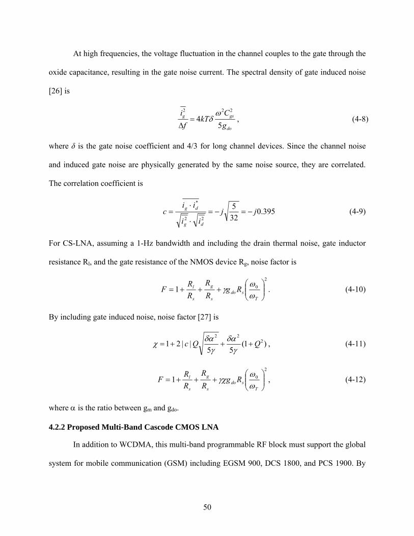
A schematic of a cascode amplifier including its output network is shown in Figure 4-3.
The input impedance of the cadcode LNA under the perfect 50-Ω input matching is
sTgs
sgin LCj
LLjZ ωω
ω +++=1)( . (4-13)
When the input impedance is perfectly matched to sR , the quality factor of input network
including the source resistance, sR is
sgs RCQ
021
ω= . (4-14)
Typically, a cascode LNA topology provides good stability because it can isolate the
Figure 4-3 Cascode LNA with inductive degeneration
52
Figure 4-4 Proposed multi-band LNA
input port from output port. This isolation makes the design more straightforward because input
matching and output marching networks can be independently specified. Both the bottom and top
transistors, M1 & M2 have the same length and width [28], [29].
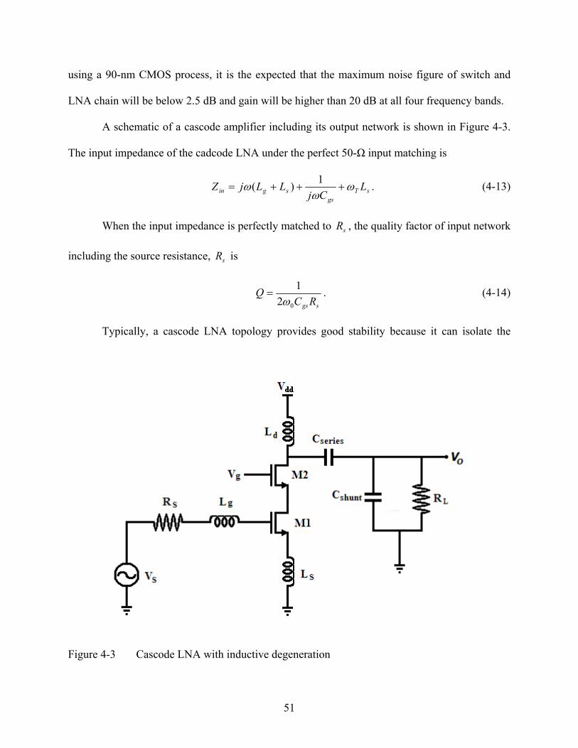
Figure 4-4 shows the proposed multi-band LNA which employs the cascode with
inductive degeneration. The input matching is realized by bond-wires, source/drain-to-gate
varactors [6] and two off-chip inductors. Here, “varactor A” is used to generate dual peaks which
provide tuning for both the lower and higher bands. “Varactor B” is used to adjust quality factor
of input network, which is needed to improve the noise performance of the circuit. Output
matching is achieved by two on-chip inductors and two accumulation mode MOS varactors. Two
on-chip inductors are connected in series between Vdd and drain of transistor M2 to provide DC
bias. “Varactor C” is used to change matching capacitance and “Varactor D” tunes the drain
inductance.
53
4.3 Input Matching of a Multi-Band LNA
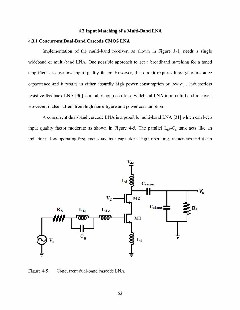
4.3.1 Concurrent Dual-Band Cascode CMOS LNA
Implementation of the multi-band receiver, as shown in Figure 3-1, needs a single
wideband or multi-band LNA. One possible approach to get a broadband matching for a tuned
amplifier is to use low input quality factor. However, this circuit requires large gate-to-source
capacitance and it results in either absurdly high power consumption or low Tω . Inductorless
resistive-feedback LNA [30] is another approach for a wideband LNA in a multi-band receiver.
However, it also suffers from high noise figure and power consumption.
A concurrent dual-band cascode LNA is a possible multi-band LNA [31] which can keep
input quality factor moderate as shown in Figure 4-5. The parallel Lg1-Cg tank acts like an
inductor at low operating frequencies and as a capacitor at high operating frequencies and it can
Figure 4-5 Concurrent dual-band cascode LNA
54
resonate with Lg2, Cgs, and Ls in series at both low and high frequency bands of interest. The high
frequency bands of interest ( DCS 1800, PCS 1900, and WCDMA ) occupy a broad frequency
band between 1805 and 2170 MHz and tenability is highly desirable this frequency range.
4.3.2 Input Matching of a Proposed Multi-Band Cascode CMOS LNA
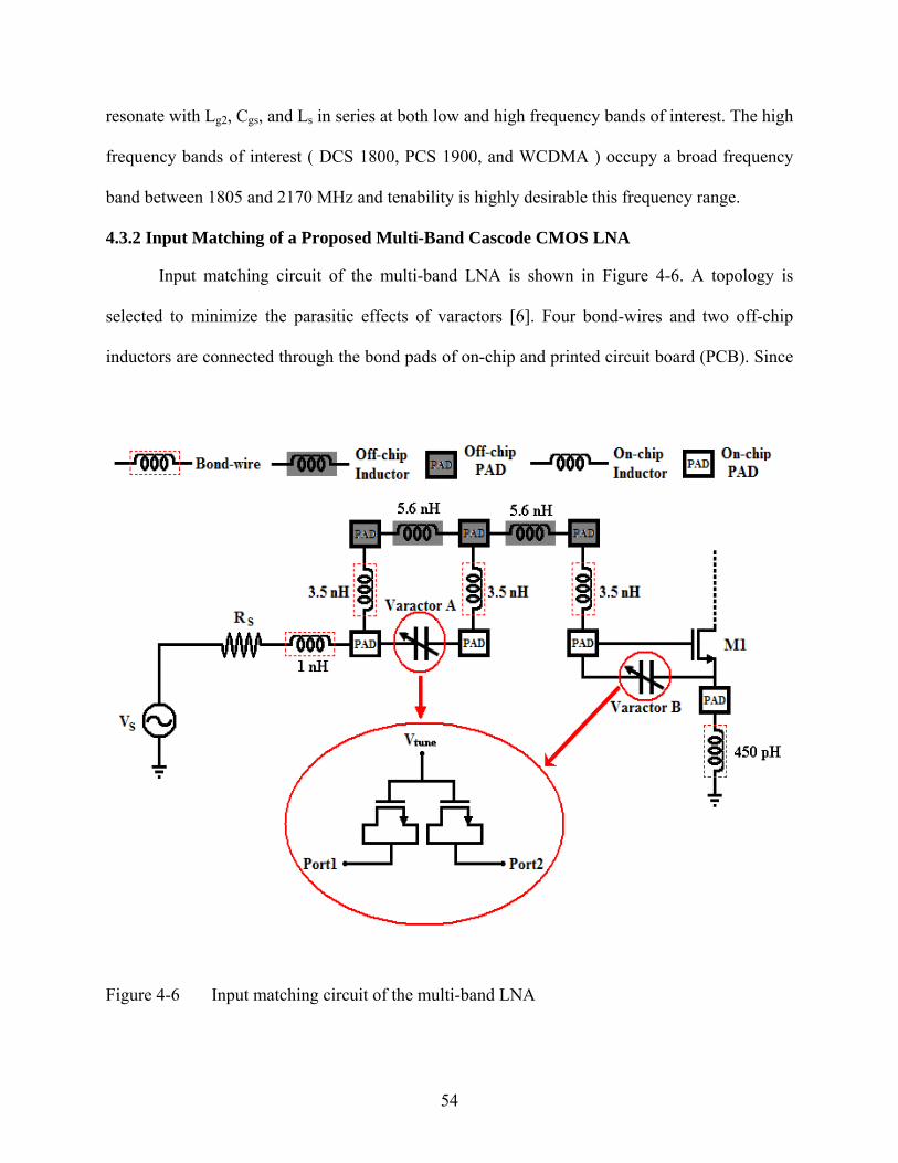
Input matching circuit of the multi-band LNA is shown in Figure 4-6. A topology is
selected to minimize the parasitic effects of varactors [6]. Four bond-wires and two off-chip
inductors are connected through the bond pads of on-chip and printed circuit board (PCB). Since
Figure 4-6 Input matching circuit of the multi-band LNA
55
the parasitic resistances of off-chip inductor and bond-wires are low, so their quality factors are
higher. Varactors A and B employ NMOS source/drain-to-gate varactors [6] which are
composed of NMOS transistors with the source and drain, connected together using metal layers.
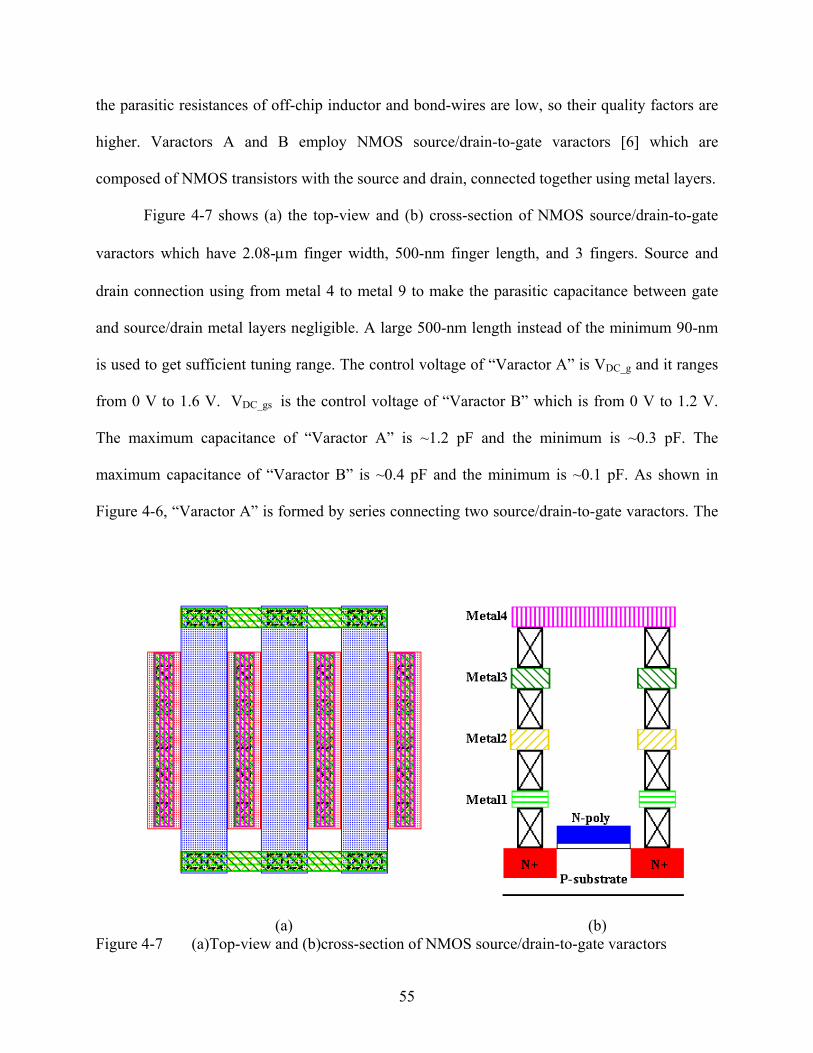
Figure 4-7 shows (a) the top-view and (b) cross-section of NMOS source/drain-to-gate
varactors which have 2.08-μm finger width, 500-nm finger length, and 3 fingers. Source and
drain connection using from metal 4 to metal 9 to make the parasitic capacitance between gate
and source/drain metal layers negligible. A large 500-nm length instead of the minimum 90-nm
is used to get sufficient tuning range. The control voltage of “Varactor A” is VDC_g and it ranges
from 0 V to 1.6 V. VDC_gs is the control voltage of “Varactor B” which is from 0 V to 1.2 V.
The maximum capacitance of “Varactor A” is ~1.2 pF and the minimum is ~0.3 pF. The
maximum capacitance of “Varactor B” is ~0.4 pF and the minimum is ~0.1 pF. As shown in
Figure 4-6, “Varactor A” is formed by series connecting two source/drain-to-gate varactors. The
(a) (b)
Figure 4-7 (a)Top-view and (b)cross-section of NMOS source/drain-to-gate varactors
56
inductance between the gate of transistor M1 and “Varactor A” plays a critical role [6] to keep
|S11|’s below -10 dB at both the high and low frequency bands.
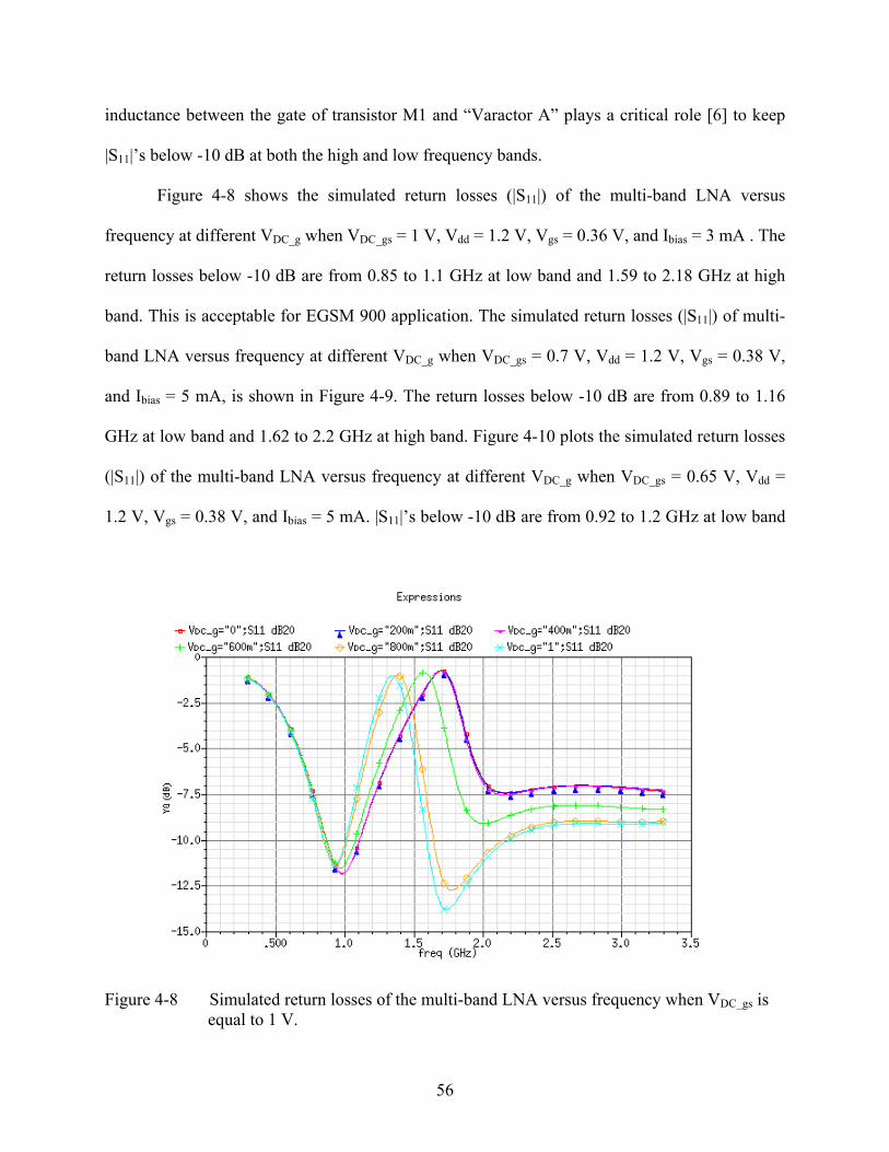
Figure 4-8 shows the simulated return losses (|S11|) of the multi-band LNA versus
frequency at different VDC_g when VDC_gs = 1 V, Vdd = 1.2 V, Vgs = 0.36 V, and Ibias = 3 mA . The
return losses below -10 dB are from 0.85 to 1.1 GHz at low band and 1.59 to 2.18 GHz at high
band. This is acceptable for EGSM 900 application. The simulated return losses (|S11|) of multi-
band LNA versus frequency at different VDC_g when VDC_gs = 0.7 V, Vdd = 1.2 V, Vgs = 0.38 V,
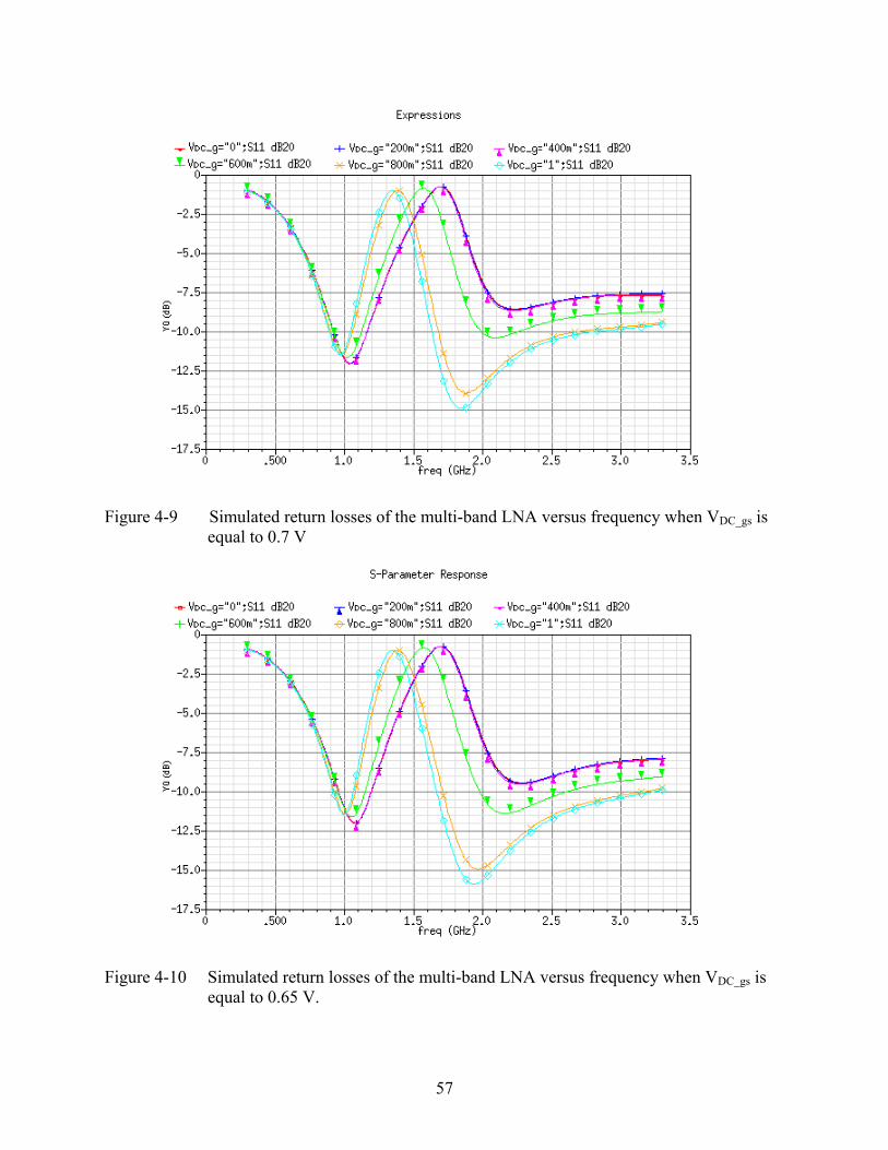
and Ibias = 5 mA, is shown in Figure 4-9. The return losses below -10 dB are from 0.89 to 1.16
GHz at low band and 1.62 to 2.2 GHz at high band. Figure 4-10 plots the simulated return losses
(|S11|) of the multi-band LNA versus frequency at different VDC_g when VDC_gs = 0.65 V, Vdd =
1.2 V, Vgs = 0.38 V, and Ibias = 5 mA. |S11|’s below -10 dB are from 0.92 to 1.2 GHz at low band
Figure 4-8 Simulated return losses of the multi-band LNA versus frequency when VDC_gs is equal to 1 V.
57
Figure 4-9 Simulated return losses of the multi-band LNA versus frequency when VDC_gs is
equal to 0.7 V
Figure 4-10 Simulated return losses of the multi-band LNA versus frequency when VDC_gs is equal to 0.65 V.
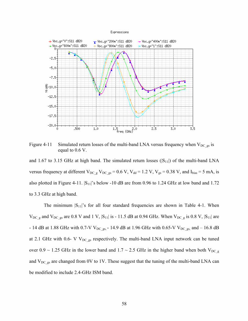
58
Figure 4-11 Simulated return losses of the multi-band LNA versus frequency when VDC_gs is
equal to 0.6 V.
and 1.67 to 3.15 GHz at high band. The simulated return losses (|S11|) of the multi-band LNA
versus frequency at different VDC_g VDC_gs = 0.6 V, Vdd = 1.2 V, Vgs = 0.38 V, and Ibias = 5 mA, is
also plotted in Figure 4-11. |S11|’s below -10 dB are from 0.96 to 1.24 GHz at low band and 1.72
to 3.3 GHz at high band.
The minimum |S11|’s for all four standard frequencies are shown in Table 4-1. When
VDC_g and VDC_gs are 0.8 V and 1 V, |S11| is - 11.5 dB at 0.94 GHz. When VDC_g is 0.8 V, |S11| are
- 14 dB at 1.88 GHz with 0.7-V VDC_gs, - 14.9 dB at 1.96 GHz with 0.65-V VDC_gs, and – 16.8 dB
at 2.1 GHz with 0.6- V VDC_gs respectively. The multi-band LNA input network can be tuned
over 0.9 ~ 1.25 GHz in the lower band and 1.7 ~ 2.5 GHz in the higher band when both VDC_g
and VDC_gs are changed from 0V to 1V. These suggest that the tuning of the multi-band LNA can
be modified to include 2.4-GHz ISM band.
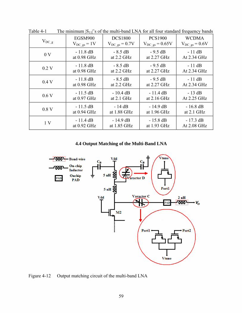
59
Table 4-1 The minimum |S11|’s of the multi-band LNA for all four standard frequency bands
VDC_g EGSM900
VDC_gs = 1V DCS1800
VDC_gs = 0.7V PCS1900
VDC_gs = 0.65V WCDMA
VDC_gs = 0.6V
0 V - 11.8 dB at 0.98 GHz
- 8.5 dB at 2.2 GHz
- 9.5 dB at 2.27 GHz
- 11 dB At 2.34 GHz
0.2 V - 11.8 dB at 0.98 GHz
- 8.5 dB at 2.2 GHz
- 9.5 dB at 2.27 GHz
- 11 dB At 2.34 GHz
0.4 V - 11.8 dB at 0.98 GHz
- 8.5 dB at 2.2 GHz
- 9.5 dB at 2.27 GHz
- 11 dB At 2.34 GHz
0.6 V - 11.5 dB at 0.97 GHz
- 10.4 dB at 2.1 GHz
- 11.4 dB at 2.16 GHz
- 13 dB At 2.25 GHz
0.8 V - 11.5 dB at 0.94 GHz
- 14 dB at 1.88 GHz
- 14.9 dB at 1.96 GHz
- 16.8 dB at 2.1 GHz
1 V - 11.4 dB at 0.92 GHz
- 14.9 dB at 1.85 GHz
- 15.8 dB at 1.93 GHz
- 17.3 dB At 2.08 GHz
4.4 Output Matching of the Multi-Band LNA
Figure 4-12 Output matching circuit of the multi-band LNA
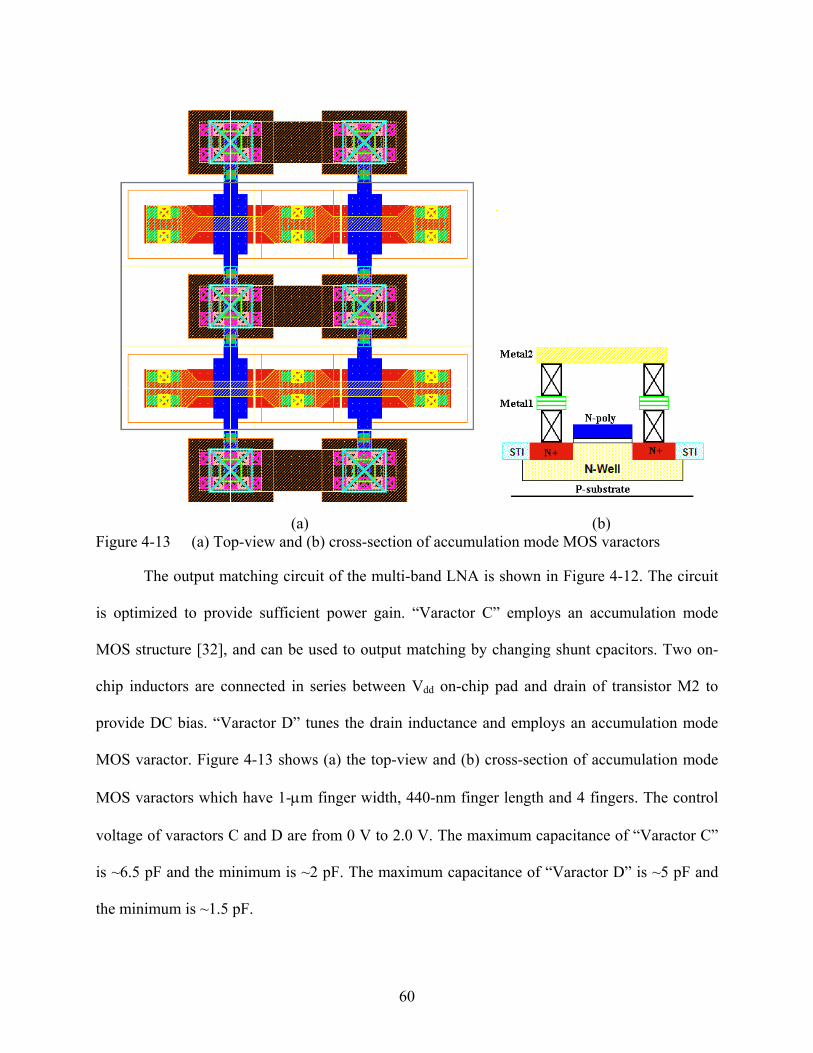
60
(a) (b)
Figure 4-13 (a) Top-view and (b) cross-section of accumulation mode MOS varactors
The output matching circuit of the multi-band LNA is shown in Figure 4-12. The circuit
is optimized to provide sufficient power gain. “Varactor C” employs an accumulation mode
MOS structure [32], and can be used to output matching by changing shunt cpacitors. Two on-
chip inductors are connected in series between Vdd on-chip pad and drain of transistor M2 to
provide DC bias. “Varactor D” tunes the drain inductance and employs an accumulation mode
MOS varactor. Figure 4-13 shows (a) the top-view and (b) cross-section of accumulation mode
MOS varactors which have 1-μm finger width, 440-nm finger length and 4 fingers. The control
voltage of varactors C and D are from 0 V to 2.0 V. The maximum capacitance of “Varactor C”
is ~6.5 pF and the minimum is ~2 pF. The maximum capacitance of “Varactor D” is ~5 pF and
the minimum is ~1.5 pF.
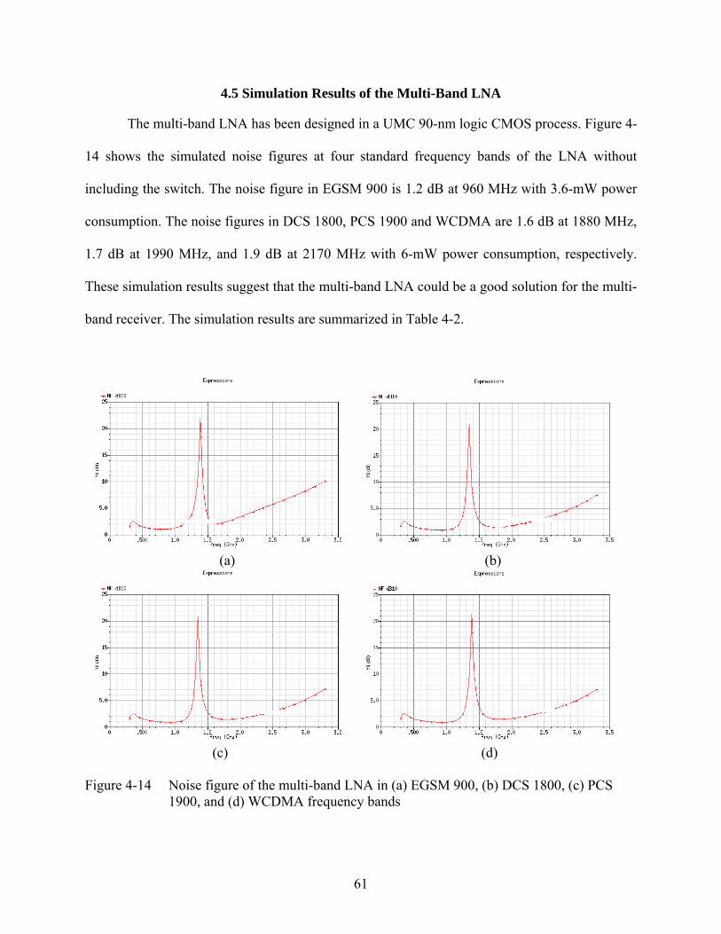
61
4.5 Simulation Results of the Multi-Band LNA
The multi-band LNA has been designed in a UMC 90-nm logic CMOS process. Figure 4-
14 shows the simulated noise figures at four standard frequency bands of the LNA without
including the switch. The noise figure in EGSM 900 is 1.2 dB at 960 MHz with 3.6-mW power
consumption. The noise figures in DCS 1800, PCS 1900 and WCDMA are 1.6 dB at 1880 MHz,
1.7 dB at 1990 MHz, and 1.9 dB at 2170 MHz with 6-mW power consumption, respectively.
These simulation results suggest that the multi-band LNA could be a good solution for the multi-
band receiver. The simulation results are summarized in Table 4-2.
(a) (b)
(c) (d)
Figure 4-14 Noise figure of the multi-band LNA in (a) EGSM 900, (b) DCS 1800, (c) PCS
1900, and (d) WCDMA frequency bands
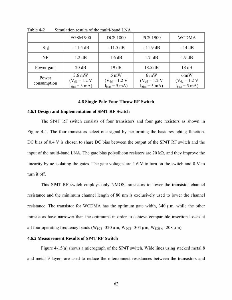
62
Table 4-2 Simulation results of the multi-band LNA
EGSM 900 DCS 1800 PCS 1900 WCDMA
|S11| - 11.5 dB - 11.5 dB - 11.9 dB - 14 dB
NF 1.2 dB 1.6 dB 1.7 dB 1.9 dB
Power gain 20 dB 19 dB 18.5 dB 18 dB
Power consumption
3.6 mW (Vdd = 1.2 V Ibias = 3 mA)
6 mW (Vdd = 1.2 V Ibias = 5 mA)
6 mW (Vdd = 1.2 V Ibias = 5 mA)
6 mW (Vdd = 1.2 V Ibias = 5 mA)
4.6 Single-Pole-Four-Throw RF Switch
4.6.1 Design and Implementation of SP4T RF Switch
The SP4T RF switch consists of four transistors and four gate resistors as shown in
Figure 4-1. The four transistors select one signal by performing the basic switching function.
DC bias of 0.4 V is chosen to share DC bias between the output of the SP4T RF switch and the
input of the multi-band LNA. The gate bias polysilicon resistors are 20 kΩ, and they improve the
linearity by ac isolating the gates. The gate voltages are 1.6 V to turn on the switch and 0 V to
turn it off.
This SP4T RF switch employs only NMOS transistors to lower the transistor channel
resistance and the minimum channel length of 80 nm is exclusively used to lower the channel
resistance. The transistor for WCDMA has the optimum gate width, 340 μm, while the other
transistors have narrower than the optimums in order to achieve comparable insertion losses at
all four operating frequency bands (WPCS=320 μm, WDCS=304 μm, WEGSM=208 μm).
4.6.2 Measurement Results of SP4T RF Switch
Figure 4-15(a) shows a micrograph of the SP4T switch. Wide lines using stacked metal 8
and metal 9 layers are used to reduce the interconnect resistances between the transistors and
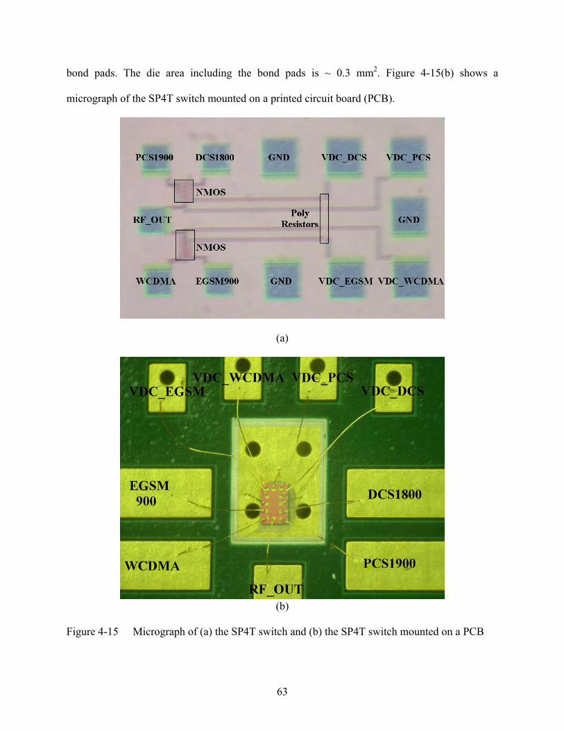
63
bond pads. The die area including the bond pads is ~ 0.3 mm2. Figure 4-15(b) shows a
micrograph of the SP4T switch mounted on a printed circuit board (PCB).
(a)
(b)
Figure 4-15 Micrograph of (a) the SP4T switch and (b) the SP4T switch mounted on a PCB
64
Figure 4-16 Measured insertion losses of the SP4T RF switch versus frequency
Figure 4-16 shows the measured insertion losses of the SP4T RF switch versus
frequency. The insertion losses of the SP4T RF switch are 0.35 dB at 960 MHz, 0.34 dB at 1880
MHz, 0.35 dB at 1990 MHz, and 0.40 dB at 2140 MHz, respectively, which are excellent.
Table 4-3 summarizes the performance of SP4T RF switch in the UMC 90-nm logic
CMOS technology. The isolations of the SP4T RF switch at EGSM 900, DCS 1800, PCS 1900,
Table 4-3 Performance of SP4T RF switch
Frequency [GHz] Insertion loss [dB]
Isolation [dB] IP1dB [dBm] IIP3 [dBm] Tech.
0.96 (EGSM) 0.35 28 13 24 90-nm
1.88 (DCS) 0.34 22 12 23 90-nm
1.99 (PCS) 0.35 21 12 23 90-nm
2.17 (WCDMA) 0.40 20 12 23 90-nm
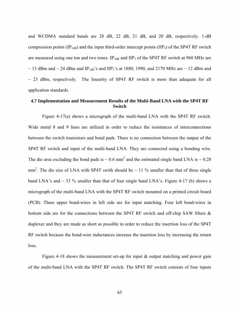
65
and WCDMA standard bands are 28 dB, 22 dB, 21 dB, and 20 dB, respectively. 1-dB
compression points (IP1dB) and the input third-order intercept points (IIP3) of the SP4T RF switch
are measured using one ton and two tones. IP1dB and IIP3 of the SP4T RF switch at 960 MHz are
~ 13 dBm and ~ 24 dBm and IP1dB’s and IIP3’s at 1880, 1990, and 2170 MHz are ~ 12 dBm and
~ 23 dBm, respectively. The linearity of SP4T RF switch is more than adequate for all
application standards.
4.7 Implementation and Measurement Results of the Multi-Band LNA with the SP4T RF Switch
Figure 4-17(a) shows a micrograph of the multi-band LNA with the SP4T RF switch.
Wide metal 8 and 9 lines are utilized in order to reduce the resistances of interconnections
between the switch transistors and bond pads. There is no connection between the output of the
SP4T RF switch and input of the multi-band LNA. They are connected using a bonding wire.
The die area excluding the bond pads is ~ 0.6 mm2 and the estimated single band LNA is ~ 0.28
mm2. The die size of LNA with SP4T swith should be ~ 11 % smaller than that of three single
band LNA’s and ~ 33 % smaller than that of four single band LNA’s. Figure 4-17 (b) shows a
micrograph of the multi-band LNA with the SP4T RF switch mounted on a printed circuit board
(PCB). Three upper bond-wires in left side are for input matching. Four left bond-wires in
bottom side are for the connections between the SP4T RF switch and off-chip SAW filters &
duplexer and they are made as short as possible in order to reduce the insertion loss of the SP4T
RF switch because the bond-wire inductances increase the insertion loss by increasing the return
loss.
Figure 4-18 shows the measurement set-up for input & output matching and power gain
of the multi-band LNA with the SP4T RF switch. The SP4T RF switch consists of four inputs
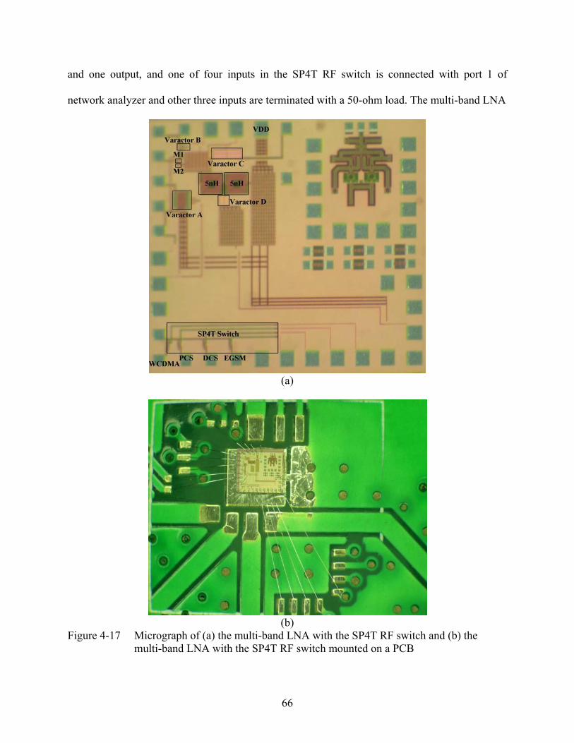
66
and one output, and one of four inputs in the SP4T RF switch is connected with port 1 of
network analyzer and other three inputs are terminated with a 50-ohm load. The multi-band LNA
(a)
(b)
Figure 4-17 Micrograph of (a) the multi-band LNA with the SP4T RF switch and (b) the multi-band LNA with the SP4T RF switch mounted on a PCB
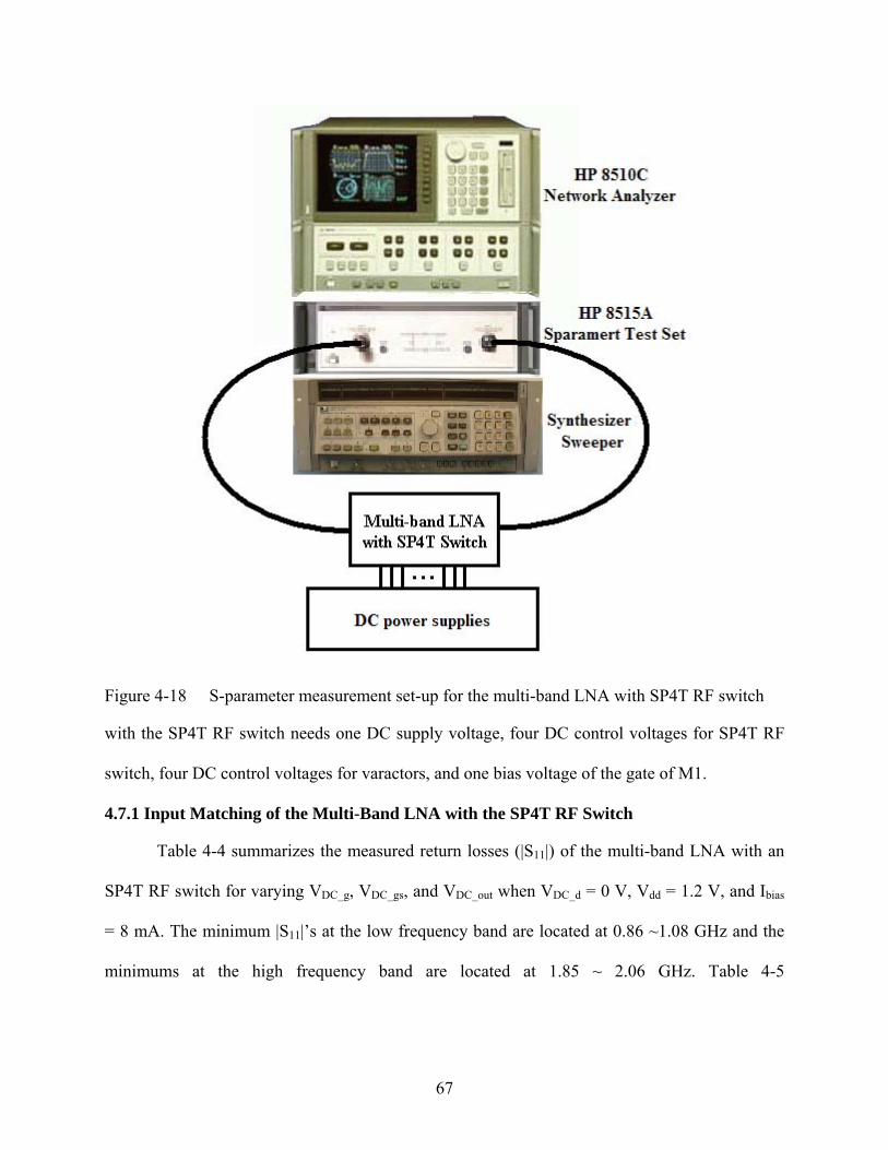
67
Figure 4-18 S-parameter measurement set-up for the multi-band LNA with SP4T RF switch
with the SP4T RF switch needs one DC supply voltage, four DC control voltages for SP4T RF
switch, four DC control voltages for varactors, and one bias voltage of the gate of M1.
4.7.1 Input Matching of the Multi-Band LNA with the SP4T RF Switch
Table 4-4 summarizes the measured return losses (|S11|) of the multi-band LNA with an
SP4T RF switch for varying VDC_g, VDC_gs, and VDC_out when VDC_d = 0 V, Vdd = 1.2 V, and Ibias
= 8 mA. The minimum |S11|’s at the low frequency band are located at 0.86 ~1.08 GHz and the
minimums at the high frequency band are located at 1.85 ~ 2.06 GHz. Table 4-5
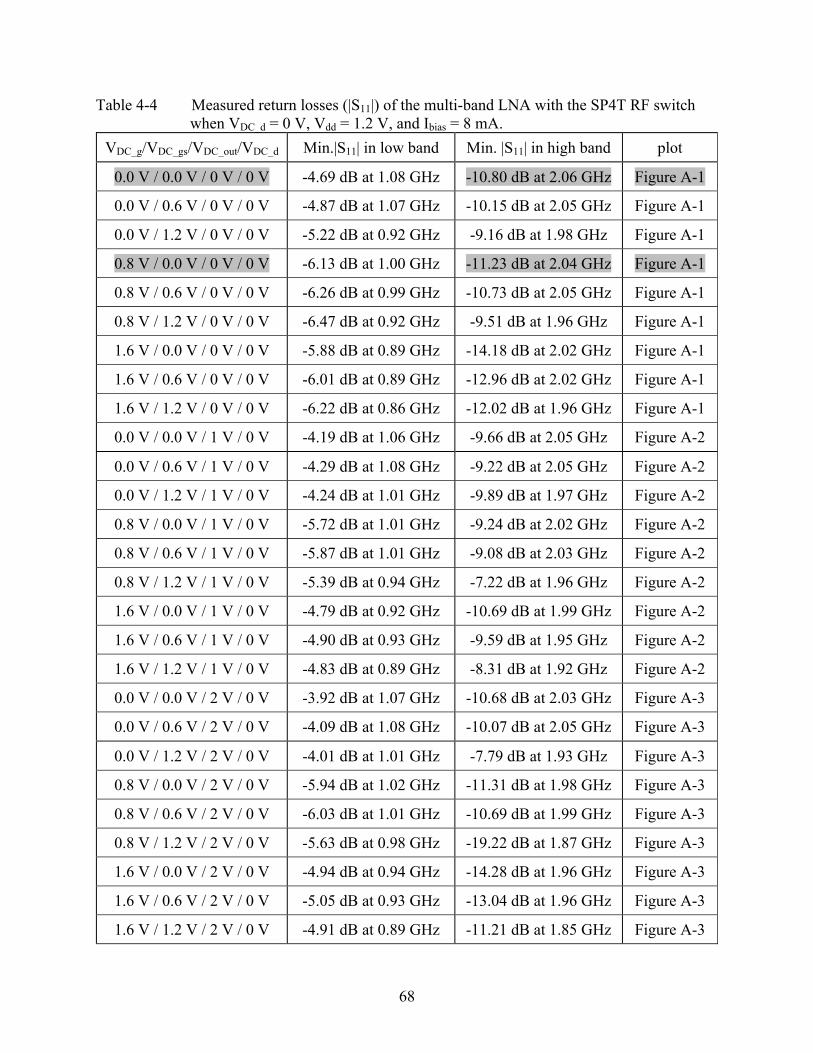
68
Table 4-4 Measured return losses (|S11|) of the multi-band LNA with the SP4T RF switch when VDC_d = 0 V, Vdd = 1.2 V, and Ibias = 8 mA.
VDC_g/VDC_gs/VDC_out/VDC_d Min.|S11| in low band Min. |S11| in high band plot
0.0 V / 0.0 V / 0 V / 0 V -4.69 dB at 1.08 GHz -10.80 dB at 2.06 GHz Figure A-1
0.0 V / 0.6 V / 0 V / 0 V -4.87 dB at 1.07 GHz -10.15 dB at 2.05 GHz Figure A-1
0.0 V / 1.2 V / 0 V / 0 V -5.22 dB at 0.92 GHz -9.16 dB at 1.98 GHz Figure A-1
0.8 V / 0.0 V / 0 V / 0 V -6.13 dB at 1.00 GHz -11.23 dB at 2.04 GHz Figure A-1
0.8 V / 0.6 V / 0 V / 0 V -6.26 dB at 0.99 GHz -10.73 dB at 2.05 GHz Figure A-1
0.8 V / 1.2 V / 0 V / 0 V -6.47 dB at 0.92 GHz -9.51 dB at 1.96 GHz Figure A-1
1.6 V / 0.0 V / 0 V / 0 V -5.88 dB at 0.89 GHz -14.18 dB at 2.02 GHz Figure A-1
1.6 V / 0.6 V / 0 V / 0 V -6.01 dB at 0.89 GHz -12.96 dB at 2.02 GHz Figure A-1
1.6 V / 1.2 V / 0 V / 0 V -6.22 dB at 0.86 GHz -12.02 dB at 1.96 GHz Figure A-1
0.0 V / 0.0 V / 1 V / 0 V -4.19 dB at 1.06 GHz -9.66 dB at 2.05 GHz Figure A-2
0.0 V / 0.6 V / 1 V / 0 V -4.29 dB at 1.08 GHz -9.22 dB at 2.05 GHz Figure A-2
0.0 V / 1.2 V / 1 V / 0 V -4.24 dB at 1.01 GHz -9.89 dB at 1.97 GHz Figure A-2
0.8 V / 0.0 V / 1 V / 0 V -5.72 dB at 1.01 GHz -9.24 dB at 2.02 GHz Figure A-2
0.8 V / 0.6 V / 1 V / 0 V -5.87 dB at 1.01 GHz -9.08 dB at 2.03 GHz Figure A-2
0.8 V / 1.2 V / 1 V / 0 V -5.39 dB at 0.94 GHz -7.22 dB at 1.96 GHz Figure A-2
1.6 V / 0.0 V / 1 V / 0 V -4.79 dB at 0.92 GHz -10.69 dB at 1.99 GHz Figure A-2
1.6 V / 0.6 V / 1 V / 0 V -4.90 dB at 0.93 GHz -9.59 dB at 1.95 GHz Figure A-2
1.6 V / 1.2 V / 1 V / 0 V -4.83 dB at 0.89 GHz -8.31 dB at 1.92 GHz Figure A-2
0.0 V / 0.0 V / 2 V / 0 V -3.92 dB at 1.07 GHz -10.68 dB at 2.03 GHz Figure A-3
0.0 V / 0.6 V / 2 V / 0 V -4.09 dB at 1.08 GHz -10.07 dB at 2.05 GHz Figure A-3
0.0 V / 1.2 V / 2 V / 0 V -4.01 dB at 1.01 GHz -7.79 dB at 1.93 GHz Figure A-3
0.8 V / 0.0 V / 2 V / 0 V -5.94 dB at 1.02 GHz -11.31 dB at 1.98 GHz Figure A-3
0.8 V / 0.6 V / 2 V / 0 V -6.03 dB at 1.01 GHz -10.69 dB at 1.99 GHz Figure A-3
0.8 V / 1.2 V / 2 V / 0 V -5.63 dB at 0.98 GHz -19.22 dB at 1.87 GHz Figure A-3
1.6 V / 0.0 V / 2 V / 0 V -4.94 dB at 0.94 GHz -14.28 dB at 1.96 GHz Figure A-3
1.6 V / 0.6 V / 2 V / 0 V -5.05 dB at 0.93 GHz -13.04 dB at 1.96 GHz Figure A-3
1.6 V / 1.2 V / 2 V / 0 V -4.91 dB at 0.89 GHz -11.21 dB at 1.85 GHz Figure A-3
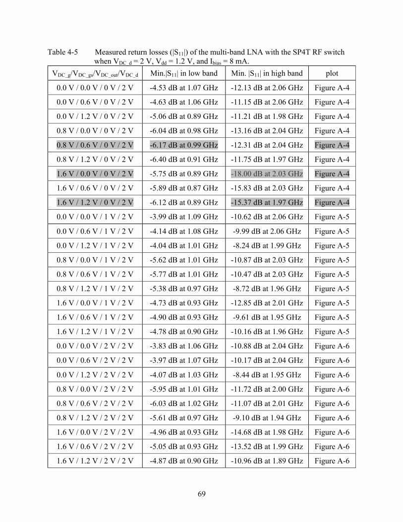
69
Table 4-5 Measured return losses (|S11|) of the multi-band LNA with the SP4T RF switch when VDC_d = 2 V, Vdd = 1.2 V, and Ibias = 8 mA.
VDC_g/VDC_gs/VDC_out/VDC_d Min.|S11| in low band Min. |S11| in high band plot
0.0 V / 0.0 V / 0 V / 2 V -4.53 dB at 1.07 GHz -12.13 dB at 2.06 GHz Figure A-4
0.0 V / 0.6 V / 0 V / 2 V -4.63 dB at 1.06 GHz -11.15 dB at 2.06 GHz Figure A-4
0.0 V / 1.2 V / 0 V / 2 V -5.06 dB at 0.89 GHz -11.21 dB at 1.98 GHz Figure A-4
0.8 V / 0.0 V / 0 V / 2 V -6.04 dB at 0.98 GHz -13.16 dB at 2.04 GHz Figure A-4
0.8 V / 0.6 V / 0 V / 2 V -6.17 dB at 0.99 GHz -12.31 dB at 2.04 GHz Figure A-4
0.8 V / 1.2 V / 0 V / 2 V -6.40 dB at 0.91 GHz -11.75 dB at 1.97 GHz Figure A-4
1.6 V / 0.0 V / 0 V / 2 V -5.75 dB at 0.89 GHz -18.00 dB at 2.03 GHz Figure A-4
1.6 V / 0.6 V / 0 V / 2 V -5.89 dB at 0.87 GHz -15.83 dB at 2.03 GHz Figure A-4
1.6 V / 1.2 V / 0 V / 2 V -6.12 dB at 0.89 GHz -15.37 dB at 1.97 GHz Figure A-4
0.0 V / 0.0 V / 1 V / 2 V -3.99 dB at 1.09 GHz -10.62 dB at 2.06 GHz Figure A-5
0.0 V / 0.6 V / 1 V / 2 V -4.14 dB at 1.08 GHz -9.99 dB at 2.06 GHz Figure A-5
0.0 V / 1.2 V / 1 V / 2 V -4.04 dB at 1.01 GHz -8.24 dB at 1.99 GHz Figure A-5
0.8 V / 0.0 V / 1 V / 2 V -5.62 dB at 1.01 GHz -10.87 dB at 2.03 GHz Figure A-5
0.8 V / 0.6 V / 1 V / 2 V -5.77 dB at 1.01 GHz -10.47 dB at 2.03 GHz Figure A-5
0.8 V / 1.2 V / 1 V / 2 V -5.38 dB at 0.97 GHz -8.72 dB at 1.96 GHz Figure A-5
1.6 V / 0.0 V / 1 V / 2 V -4.73 dB at 0.93 GHz -12.85 dB at 2.01 GHz Figure A-5
1.6 V / 0.6 V / 1 V / 2 V -4.90 dB at 0.93 GHz -9.61 dB at 1.95 GHz Figure A-5
1.6 V / 1.2 V / 1 V / 2 V -4.78 dB at 0.90 GHz -10.16 dB at 1.96 GHz Figure A-5
0.0 V / 0.0 V / 2 V / 2 V -3.83 dB at 1.06 GHz -10.88 dB at 2.04 GHz Figure A-6
0.0 V / 0.6 V / 2 V / 2 V -3.97 dB at 1.07 GHz -10.17 dB at 2.04 GHz Figure A-6
0.0 V / 1.2 V / 2 V / 2 V -4.07 dB at 1.03 GHz -8.44 dB at 1.95 GHz Figure A-6
0.8 V / 0.0 V / 2 V / 2 V -5.95 dB at 1.01 GHz -11.72 dB at 2.00 GHz Figure A-6
0.8 V / 0.6 V / 2 V / 2 V -6.03 dB at 1.02 GHz -11.07 dB at 2.01 GHz Figure A-6
0.8 V / 1.2 V / 2 V / 2 V -5.61 dB at 0.97 GHz -9.10 dB at 1.94 GHz Figure A-6
1.6 V / 0.0 V / 2 V / 2 V -4.96 dB at 0.93 GHz -14.68 dB at 1.98 GHz Figure A-6
1.6 V / 0.6 V / 2 V / 2 V -5.05 dB at 0.93 GHz -13.52 dB at 1.99 GHz Figure A-6
1.6 V / 1.2 V / 2 V / 2 V -4.87 dB at 0.90 GHz -10.96 dB at 1.89 GHz Figure A-6
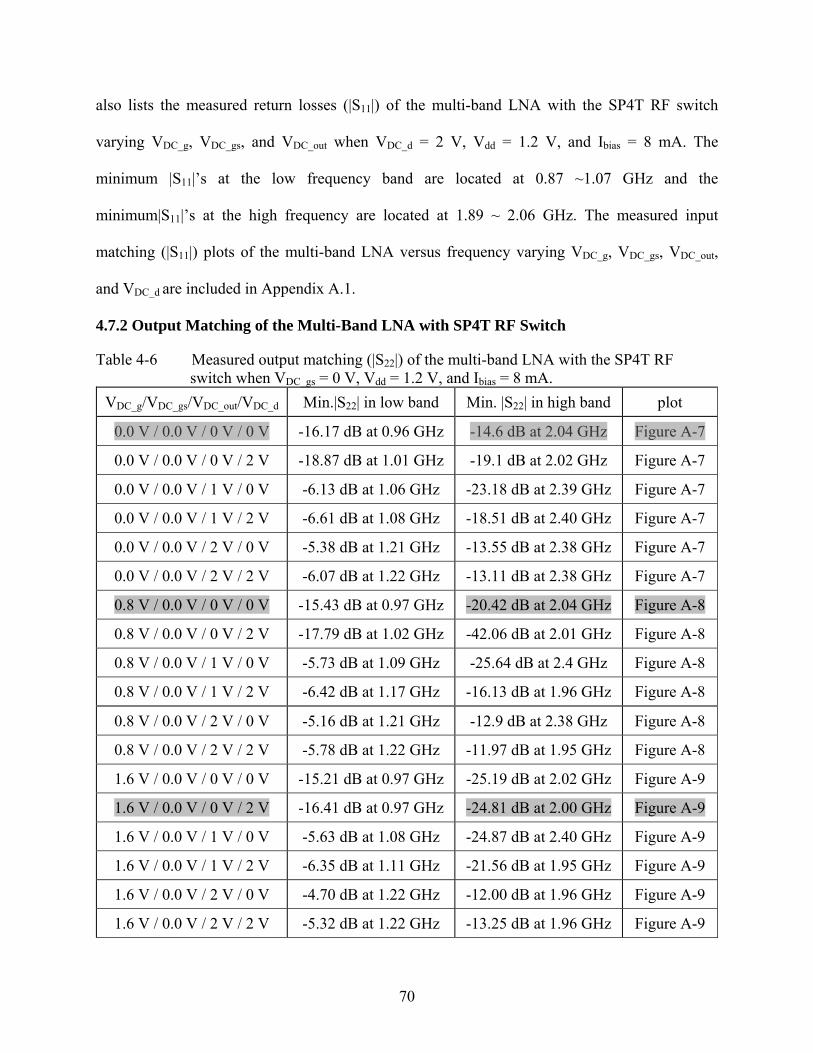
70
also lists the measured return losses (|S11|) of the multi-band LNA with the SP4T RF switch
varying VDC_g, VDC_gs, and VDC_out when VDC_d = 2 V, Vdd = 1.2 V, and Ibias = 8 mA. The
minimum |S11|’s at the low frequency band are located at 0.87 ~1.07 GHz and the
minimum|S11|’s at the high frequency are located at 1.89 ~ 2.06 GHz. The measured input
matching (|S11|) plots of the multi-band LNA versus frequency varying VDC_g, VDC_gs, VDC_out,
and VDC_d are included in Appendix A.1.
4.7.2 Output Matching of the Multi-Band LNA with SP4T RF Switch
Table 4-6 Measured output matching (|S22|) of the multi-band LNA with the SP4T RF switch when VDC_gs = 0 V, Vdd = 1.2 V, and Ibias = 8 mA.
VDC_g/VDC_gs/VDC_out/VDC_d Min.|S22| in low band Min. |S22| in high band plot
0.0 V / 0.0 V / 0 V / 0 V -16.17 dB at 0.96 GHz -14.6 dB at 2.04 GHz Figure A-7
0.0 V / 0.0 V / 0 V / 2 V -18.87 dB at 1.01 GHz -19.1 dB at 2.02 GHz Figure A-7
0.0 V / 0.0 V / 1 V / 0 V -6.13 dB at 1.06 GHz -23.18 dB at 2.39 GHz Figure A-7
0.0 V / 0.0 V / 1 V / 2 V -6.61 dB at 1.08 GHz -18.51 dB at 2.40 GHz Figure A-7
0.0 V / 0.0 V / 2 V / 0 V -5.38 dB at 1.21 GHz -13.55 dB at 2.38 GHz Figure A-7
0.0 V / 0.0 V / 2 V / 2 V -6.07 dB at 1.22 GHz -13.11 dB at 2.38 GHz Figure A-7
0.8 V / 0.0 V / 0 V / 0 V -15.43 dB at 0.97 GHz -20.42 dB at 2.04 GHz Figure A-8
0.8 V / 0.0 V / 0 V / 2 V -17.79 dB at 1.02 GHz -42.06 dB at 2.01 GHz Figure A-8
0.8 V / 0.0 V / 1 V / 0 V -5.73 dB at 1.09 GHz -25.64 dB at 2.4 GHz Figure A-8
0.8 V / 0.0 V / 1 V / 2 V -6.42 dB at 1.17 GHz -16.13 dB at 1.96 GHz Figure A-8
0.8 V / 0.0 V / 2 V / 0 V -5.16 dB at 1.21 GHz -12.9 dB at 2.38 GHz Figure A-8
0.8 V / 0.0 V / 2 V / 2 V -5.78 dB at 1.22 GHz -11.97 dB at 1.95 GHz Figure A-8
1.6 V / 0.0 V / 0 V / 0 V -15.21 dB at 0.97 GHz -25.19 dB at 2.02 GHz Figure A-9
1.6 V / 0.0 V / 0 V / 2 V -16.41 dB at 0.97 GHz -24.81 dB at 2.00 GHz Figure A-9
1.6 V / 0.0 V / 1 V / 0 V -5.63 dB at 1.08 GHz -24.87 dB at 2.40 GHz Figure A-9
1.6 V / 0.0 V / 1 V / 2 V -6.35 dB at 1.11 GHz -21.56 dB at 1.95 GHz Figure A-9
1.6 V / 0.0 V / 2 V / 0 V -4.70 dB at 1.22 GHz -12.00 dB at 1.96 GHz Figure A-9
1.6 V / 0.0 V / 2 V / 2 V -5.32 dB at 1.22 GHz -13.25 dB at 1.96 GHz Figure A-9
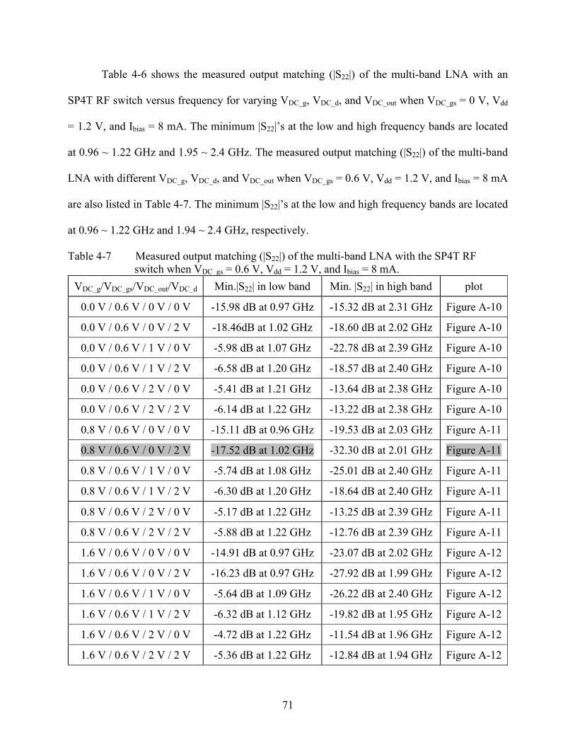
71
Table 4-6 shows the measured output matching (|S22|) of the multi-band LNA with an
SP4T RF switch versus frequency for varying VDC_g, VDC_d, and VDC_out when VDC_gs = 0 V, Vdd
= 1.2 V, and Ibias = 8 mA. The minimum |S22|’s at the low and high frequency bands are located
at 0.96 ~ 1.22 GHz and 1.95 ~ 2.4 GHz. The measured output matching (|S22|) of the multi-band
LNA with different VDC_g, VDC_d, and VDC_out when VDC_gs = 0.6 V, Vdd = 1.2 V, and Ibias = 8 mA
are also listed in Table 4-7. The minimum |S22|’s at the low and high frequency bands are located
at 0.96 ~ 1.22 GHz and 1.94 ~ 2.4 GHz, respectively.
Table 4-7 Measured output matching (|S22|) of the multi-band LNA with the SP4T RF switch when VDC_gs = 0.6 V, Vdd = 1.2 V, and Ibias = 8 mA.
VDC_g/VDC_gs/VDC_out/VDC_d Min.|S22| in low band Min. |S22| in high band plot
0.0 V / 0.6 V / 0 V / 0 V -15.98 dB at 0.97 GHz -15.32 dB at 2.31 GHz Figure A-10
0.0 V / 0.6 V / 0 V / 2 V -18.46dB at 1.02 GHz -18.60 dB at 2.02 GHz Figure A-10
0.0 V / 0.6 V / 1 V / 0 V -5.98 dB at 1.07 GHz -22.78 dB at 2.39 GHz Figure A-10
0.0 V / 0.6 V / 1 V / 2 V -6.58 dB at 1.20 GHz -18.57 dB at 2.40 GHz Figure A-10
0.0 V / 0.6 V / 2 V / 0 V -5.41 dB at 1.21 GHz -13.64 dB at 2.38 GHz Figure A-10
0.0 V / 0.6 V / 2 V / 2 V -6.14 dB at 1.22 GHz -13.22 dB at 2.38 GHz Figure A-10
0.8 V / 0.6 V / 0 V / 0 V -15.11 dB at 0.96 GHz -19.53 dB at 2.03 GHz Figure A-11
0.8 V / 0.6 V / 0 V / 2 V -17.52 dB at 1.02 GHz -32.30 dB at 2.01 GHz Figure A-11
0.8 V / 0.6 V / 1 V / 0 V -5.74 dB at 1.08 GHz -25.01 dB at 2.40 GHz Figure A-11
0.8 V / 0.6 V / 1 V / 2 V -6.30 dB at 1.20 GHz -18.64 dB at 2.40 GHz Figure A-11
0.8 V / 0.6 V / 2 V / 0 V -5.17 dB at 1.22 GHz -13.25 dB at 2.39 GHz Figure A-11
0.8 V / 0.6 V / 2 V / 2 V -5.88 dB at 1.22 GHz -12.76 dB at 2.39 GHz Figure A-11
1.6 V / 0.6 V / 0 V / 0 V -14.91 dB at 0.97 GHz -23.07 dB at 2.02 GHz Figure A-12
1.6 V / 0.6 V / 0 V / 2 V -16.23 dB at 0.97 GHz -27.92 dB at 1.99 GHz Figure A-12
1.6 V / 0.6 V / 1 V / 0 V -5.64 dB at 1.09 GHz -26.22 dB at 2.40 GHz Figure A-12
1.6 V / 0.6 V / 1 V / 2 V -6.32 dB at 1.12 GHz -19.82 dB at 1.95 GHz Figure A-12
1.6 V / 0.6 V / 2 V / 0 V -4.72 dB at 1.22 GHz -11.54 dB at 1.96 GHz Figure A-12
1.6 V / 0.6 V / 2 V / 2 V -5.36 dB at 1.22 GHz -12.84 dB at 1.94 GHz Figure A-12
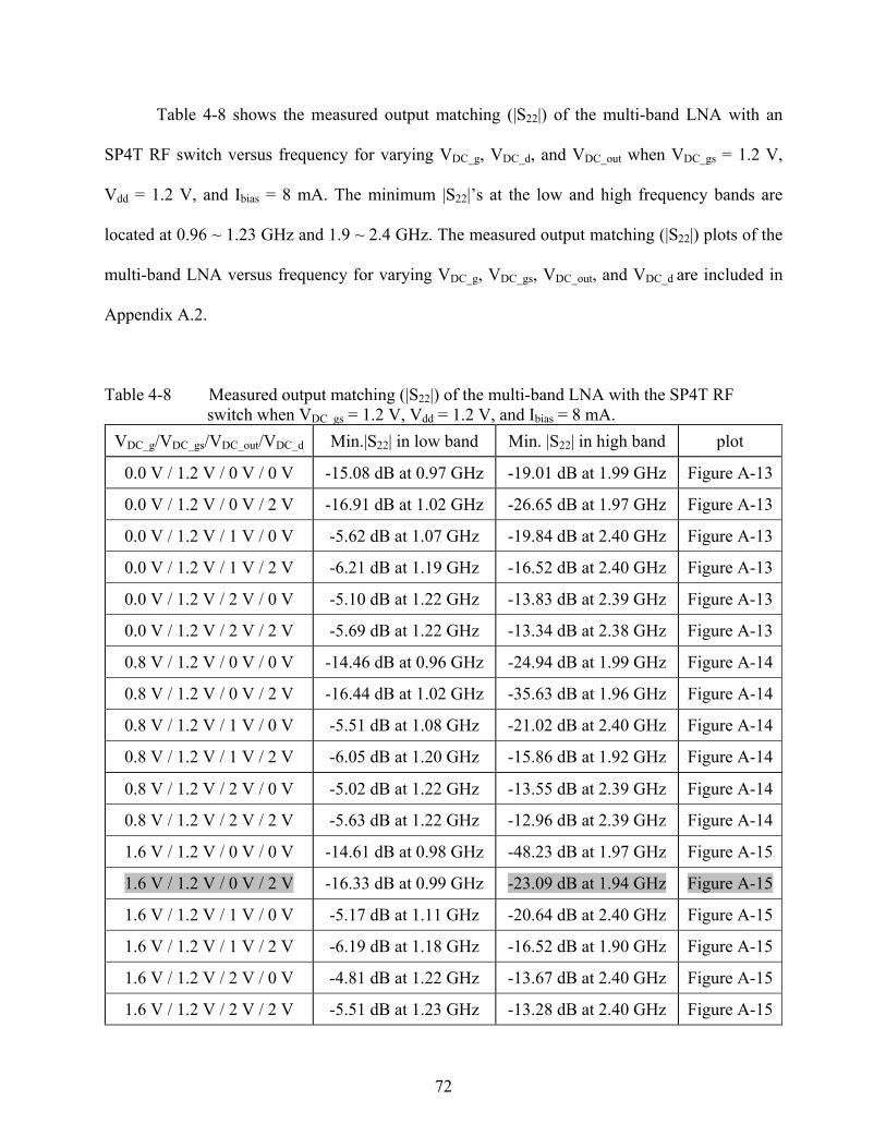
72
Table 4-8 shows the measured output matching (|S22|) of the multi-band LNA with an
SP4T RF switch versus frequency for varying VDC_g, VDC_d, and VDC_out when VDC_gs = 1.2 V,
Vdd = 1.2 V, and Ibias = 8 mA. The minimum |S22|’s at the low and high frequency bands are
located at 0.96 ~ 1.23 GHz and 1.9 ~ 2.4 GHz. The measured output matching (|S22|) plots of the
multi-band LNA versus frequency for varying VDC_g, VDC_gs, VDC_out, and VDC_d are included in
Appendix A.2.
Table 4-8 Measured output matching (|S22|) of the multi-band LNA with the SP4T RF switch when VDC_gs = 1.2 V, Vdd = 1.2 V, and Ibias = 8 mA.
VDC_g/VDC_gs/VDC_out/VDC_d Min.|S22| in low band Min. |S22| in high band plot
0.0 V / 1.2 V / 0 V / 0 V -15.08 dB at 0.97 GHz -19.01 dB at 1.99 GHz Figure A-13
0.0 V / 1.2 V / 0 V / 2 V -16.91 dB at 1.02 GHz -26.65 dB at 1.97 GHz Figure A-13
0.0 V / 1.2 V / 1 V / 0 V -5.62 dB at 1.07 GHz -19.84 dB at 2.40 GHz Figure A-13
0.0 V / 1.2 V / 1 V / 2 V -6.21 dB at 1.19 GHz -16.52 dB at 2.40 GHz Figure A-13
0.0 V / 1.2 V / 2 V / 0 V -5.10 dB at 1.22 GHz -13.83 dB at 2.39 GHz Figure A-13
0.0 V / 1.2 V / 2 V / 2 V -5.69 dB at 1.22 GHz -13.34 dB at 2.38 GHz Figure A-13
0.8 V / 1.2 V / 0 V / 0 V -14.46 dB at 0.96 GHz -24.94 dB at 1.99 GHz Figure A-14
0.8 V / 1.2 V / 0 V / 2 V -16.44 dB at 1.02 GHz -35.63 dB at 1.96 GHz Figure A-14
0.8 V / 1.2 V / 1 V / 0 V -5.51 dB at 1.08 GHz -21.02 dB at 2.40 GHz Figure A-14
0.8 V / 1.2 V / 1 V / 2 V -6.05 dB at 1.20 GHz -15.86 dB at 1.92 GHz Figure A-14
0.8 V / 1.2 V / 2 V / 0 V -5.02 dB at 1.22 GHz -13.55 dB at 2.39 GHz Figure A-14
0.8 V / 1.2 V / 2 V / 2 V -5.63 dB at 1.22 GHz -12.96 dB at 2.39 GHz Figure A-14
1.6 V / 1.2 V / 0 V / 0 V -14.61 dB at 0.98 GHz -48.23 dB at 1.97 GHz Figure A-15
1.6 V / 1.2 V / 0 V / 2 V -16.33 dB at 0.99 GHz -23.09 dB at 1.94 GHz Figure A-15
1.6 V / 1.2 V / 1 V / 0 V -5.17 dB at 1.11 GHz -20.64 dB at 2.40 GHz Figure A-15
1.6 V / 1.2 V / 1 V / 2 V -6.19 dB at 1.18 GHz -16.52 dB at 1.90 GHz Figure A-15
1.6 V / 1.2 V / 2 V / 0 V -4.81 dB at 1.22 GHz -13.67 dB at 2.40 GHz Figure A-15
1.6 V / 1.2 V / 2 V / 2 V -5.51 dB at 1.23 GHz -13.28 dB at 2.40 GHz Figure A-15
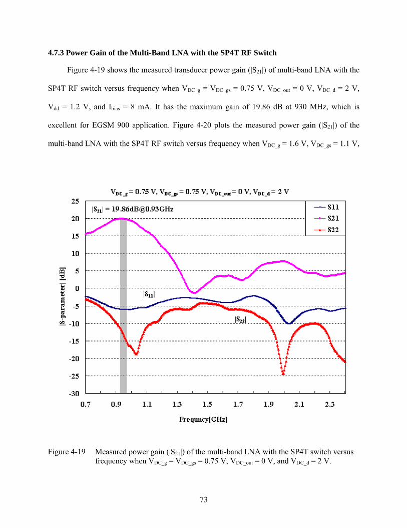
73
4.7.3 Power Gain of the Multi-Band LNA with the SP4T RF Switch
Figure 4-19 shows the measured transducer power gain (|S21|) of multi-band LNA with the
SP4T RF switch versus frequency when VDC_g = VDC_gs = 0.75 V, VDC_out = 0 V, VDC_d = 2 V,
Vdd = 1.2 V, and Ibias = 8 mA. It has the maximum gain of 19.86 dB at 930 MHz, which is
excellent for EGSM 900 application. Figure 4-20 plots the measured power gain (|S21|) of the
multi-band LNA with the SP4T RF switch versus frequency when VDC_g = 1.6 V, VDC_gs = 1.1 V,
Figure 4-19 Measured power gain (|S21|) of the multi-band LNA with the SP4T switch versus
frequency when VDC_g = VDC_gs = 0.75 V, VDC_out = 0 V, and VDC_d = 2 V.
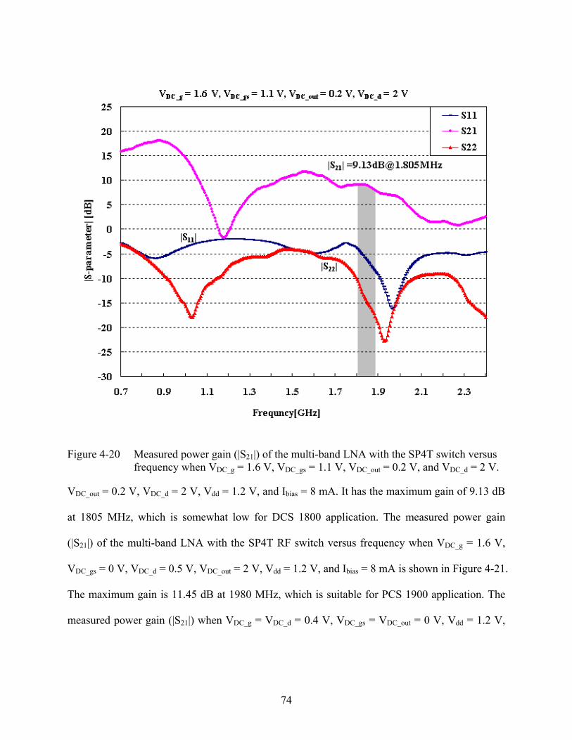
74
Figure 4-20 Measured power gain (|S21|) of the multi-band LNA with the SP4T switch versus frequency when VDC_g = 1.6 V, VDC_gs = 1.1 V, VDC_out = 0.2 V, and VDC_d = 2 V.
VDC_out = 0.2 V, VDC_d = 2 V, Vdd = 1.2 V, and Ibias = 8 mA. It has the maximum gain of 9.13 dB
at 1805 MHz, which is somewhat low for DCS 1800 application. The measured power gain
(|S21|) of the multi-band LNA with the SP4T RF switch versus frequency when VDC_g = 1.6 V,
VDC_gs = 0 V, VDC_d = 0.5 V, VDC_out = 2 V, Vdd = 1.2 V, and Ibias = 8 mA is shown in Figure 4-21.
The maximum gain is 11.45 dB at 1980 MHz, which is suitable for PCS 1900 application. The
measured power gain (|S21|) when VDC_g = VDC_d = 0.4 V, VDC_gs = VDC_out = 0 V, Vdd = 1.2 V,
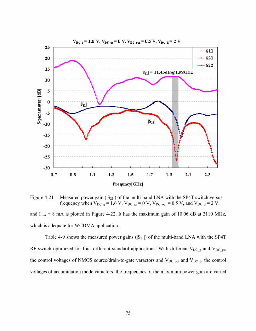
75
Figure 4-21 Measured power gain (|S21|) of the multi-band LNA with the SP4T switch versus
frequency when VDC_g = 1.6 V, VDC_gs = 0 V, VDC_out = 0.5 V, and VDC_d = 2 V.
and Ibias = 8 mA is plotted in Figure 4-22. It has the maximum gain of 10.06 dB at 2110 MHz,
which is adequate for WCDMA application.
Table 4-9 shows the measured power gains (|S21|) of the multi-band LNA with the SP4T
RF switch optimized for four different standard applications. With different VDC_g and VDC_gs,
the control voltages of NMOS source/drain-to-gate varactors and VDC_out and VDC_d, the control
voltages of accumulation mode varactors, the frequencies of the maximum power gain are varied
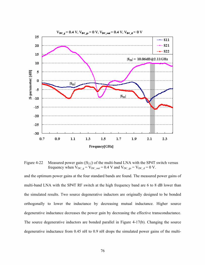
76
Figure 4-22 Measured power gain (|S21|) of the multi-band LNA with the SP4T switch versus frequency when VDC_g = VDC_out = 0.4 V and VDC_gs = VDC_d = 0 V.
and the optimum power gains at the four standard bands are found. The measured power gains of
multi-band LNA with the SP4T RF switch at the high frequency band are 6 to 8 dB lower than
the simulated results. Two source degenerative inductors are originally designed to be bonded
orthogonally to lower the inductance by decreasing mutual inductance. Higher source
degenerative inductance decreases the power gain by decreasing the effective transconductance.
The source degenerative inductors are bonded parallel in Figure 4-17(b). Changing the source
degenerative inductance from 0.45 nH to 0.9 nH drops the simulated power gains of the multi-
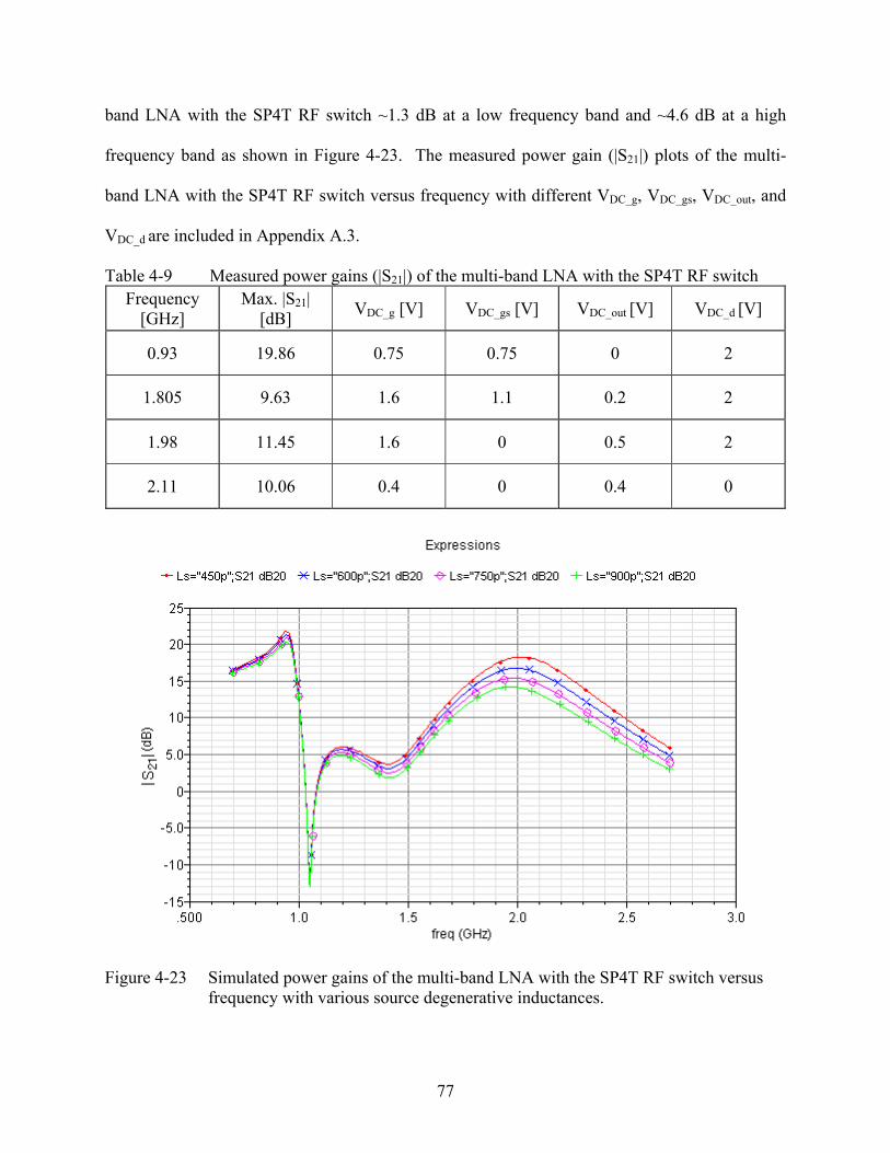
77
band LNA with the SP4T RF switch ~1.3 dB at a low frequency band and ~4.6 dB at a high
frequency band as shown in Figure 4-23. The measured power gain (|S21|) plots of the multi-
band LNA with the SP4T RF switch versus frequency with different VDC_g, VDC_gs, VDC_out, and
VDC_d are included in Appendix A.3.
Table 4-9 Measured power gains (|S21|) of the multi-band LNA with the SP4T RF switch Frequency
[GHz] Max. |S21|
[dB] VDC_g [V] VDC_gs [V] VDC_out [V] VDC_d [V]
0.93 19.86 0.75 0.75 0 2
1.805 9.63 1.6 1.1 0.2 2
1.98 11.45 1.6 0 0.5 2
2.11 10.06 0.4 0 0.4 0
Figure 4-23 Simulated power gains of the multi-band LNA with the SP4T RF switch versus
frequency with various source degenerative inductances.
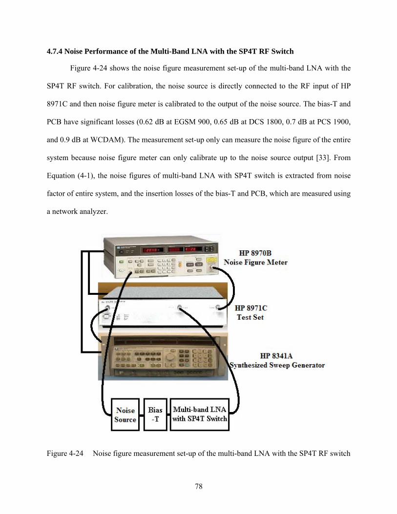
78
4.7.4 Noise Performance of the Multi-Band LNA with the SP4T RF Switch
Figure 4-24 shows the noise figure measurement set-up of the multi-band LNA with the
SP4T RF switch. For calibration, the noise source is directly connected to the RF input of HP
8971C and then noise figure meter is calibrated to the output of the noise source. The bias-T and
PCB have significant losses (0.62 dB at EGSM 900, 0.65 dB at DCS 1800, 0.7 dB at PCS 1900,
and 0.9 dB at WCDAM). The measurement set-up only can measure the noise figure of the entire
system because noise figure meter can only calibrate up to the noise source output [33]. From
Equation (4-1), the noise figures of multi-band LNA with SP4T switch is extracted from noise
factor of entire system, and the insertion losses of the bias-T and PCB, which are measured using
a network analyzer.
Figure 4-24 Noise figure measurement set-up of the multi-band LNA with the SP4T RF switch
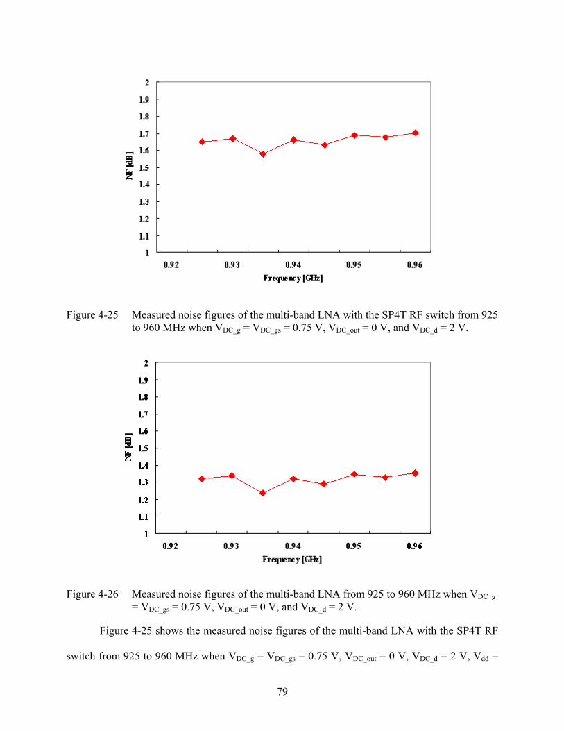
79
Figure 4-25 Measured noise figures of the multi-band LNA with the SP4T RF switch from 925 to 960 MHz when VDC_g = VDC_gs = 0.75 V, VDC_out = 0 V, and VDC_d = 2 V.
Figure 4-26 Measured noise figures of the multi-band LNA from 925 to 960 MHz when VDC_g = VDC_gs = 0.75 V, VDC_out = 0 V, and VDC_d = 2 V.
Figure 4-25 shows the measured noise figures of the multi-band LNA with the SP4T RF
switch from 925 to 960 MHz when VDC_g = VDC_gs = 0.75 V, VDC_out = 0 V, VDC_d = 2 V, Vdd =
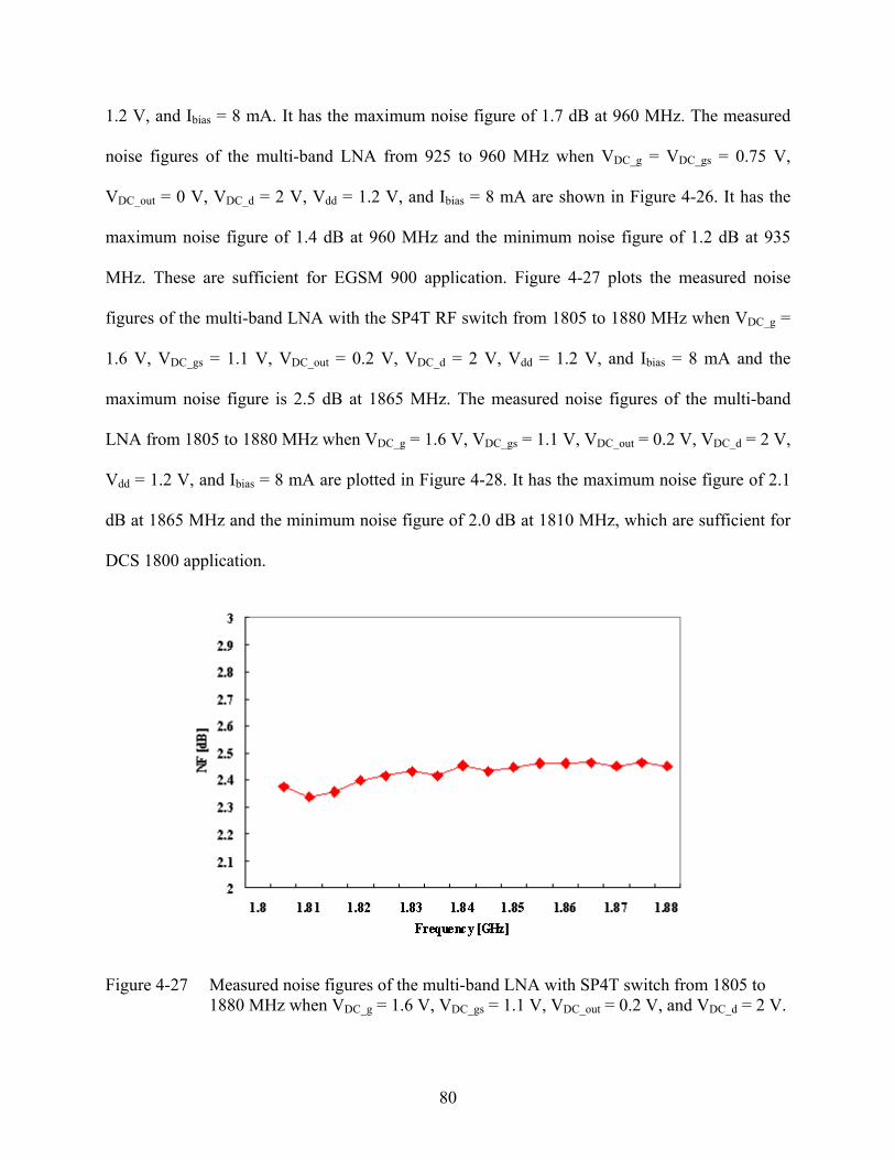
80
1.2 V, and Ibias = 8 mA. It has the maximum noise figure of 1.7 dB at 960 MHz. The measured
noise figures of the multi-band LNA from 925 to 960 MHz when VDC_g = VDC_gs = 0.75 V,
VDC_out = 0 V, VDC_d = 2 V, Vdd = 1.2 V, and Ibias = 8 mA are shown in Figure 4-26. It has the
maximum noise figure of 1.4 dB at 960 MHz and the minimum noise figure of 1.2 dB at 935
MHz. These are sufficient for EGSM 900 application. Figure 4-27 plots the measured noise
figures of the multi-band LNA with the SP4T RF switch from 1805 to 1880 MHz when VDC_g =
1.6 V, VDC_gs = 1.1 V, VDC_out = 0.2 V, VDC_d = 2 V, Vdd = 1.2 V, and Ibias = 8 mA and the
maximum noise figure is 2.5 dB at 1865 MHz. The measured noise figures of the multi-band
LNA from 1805 to 1880 MHz when VDC_g = 1.6 V, VDC_gs = 1.1 V, VDC_out = 0.2 V, VDC_d = 2 V,
Vdd = 1.2 V, and Ibias = 8 mA are plotted in Figure 4-28. It has the maximum noise figure of 2.1
dB at 1865 MHz and the minimum noise figure of 2.0 dB at 1810 MHz, which are sufficient for
DCS 1800 application.
Figure 4-27 Measured noise figures of the multi-band LNA with SP4T switch from 1805 to 1880 MHz when VDC_g = 1.6 V, VDC_gs = 1.1 V, VDC_out = 0.2 V, and VDC_d = 2 V.
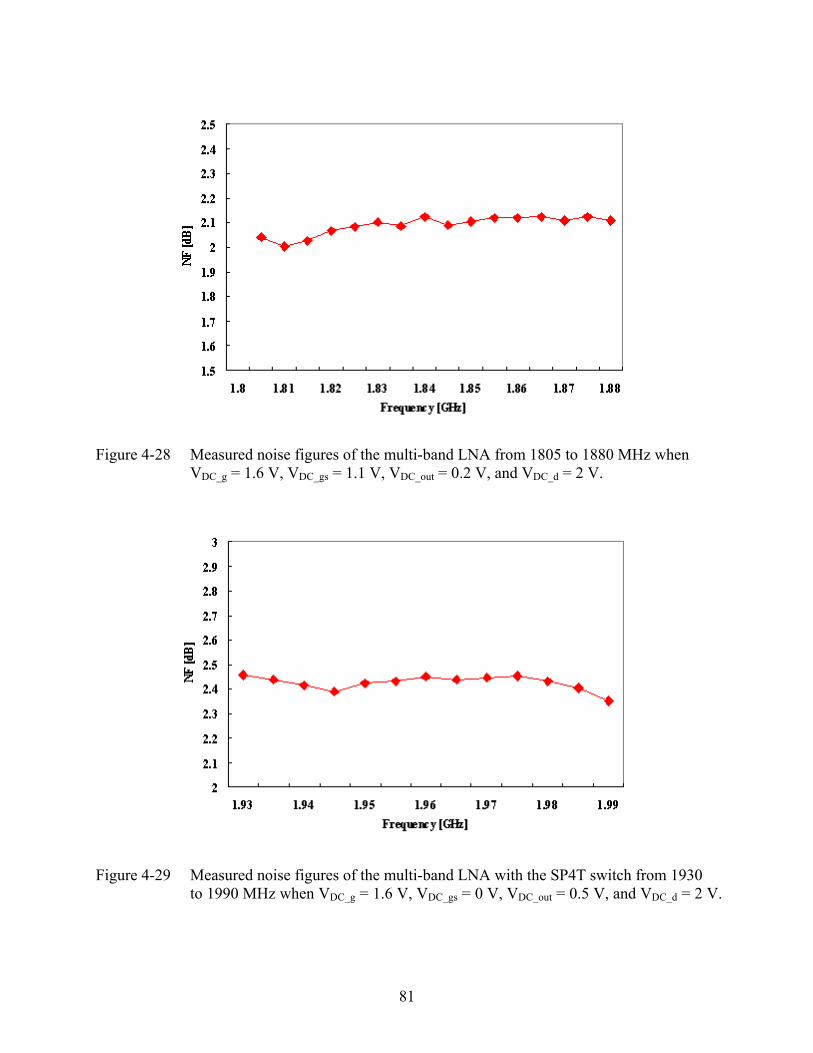
81
Figure 4-28 Measured noise figures of the multi-band LNA from 1805 to 1880 MHz when
VDC_g = 1.6 V, VDC_gs = 1.1 V, VDC_out = 0.2 V, and VDC_d = 2 V.
Figure 4-29 Measured noise figures of the multi-band LNA with the SP4T switch from 1930 to 1990 MHz when VDC_g = 1.6 V, VDC_gs = 0 V, VDC_out = 0.5 V, and VDC_d = 2 V.
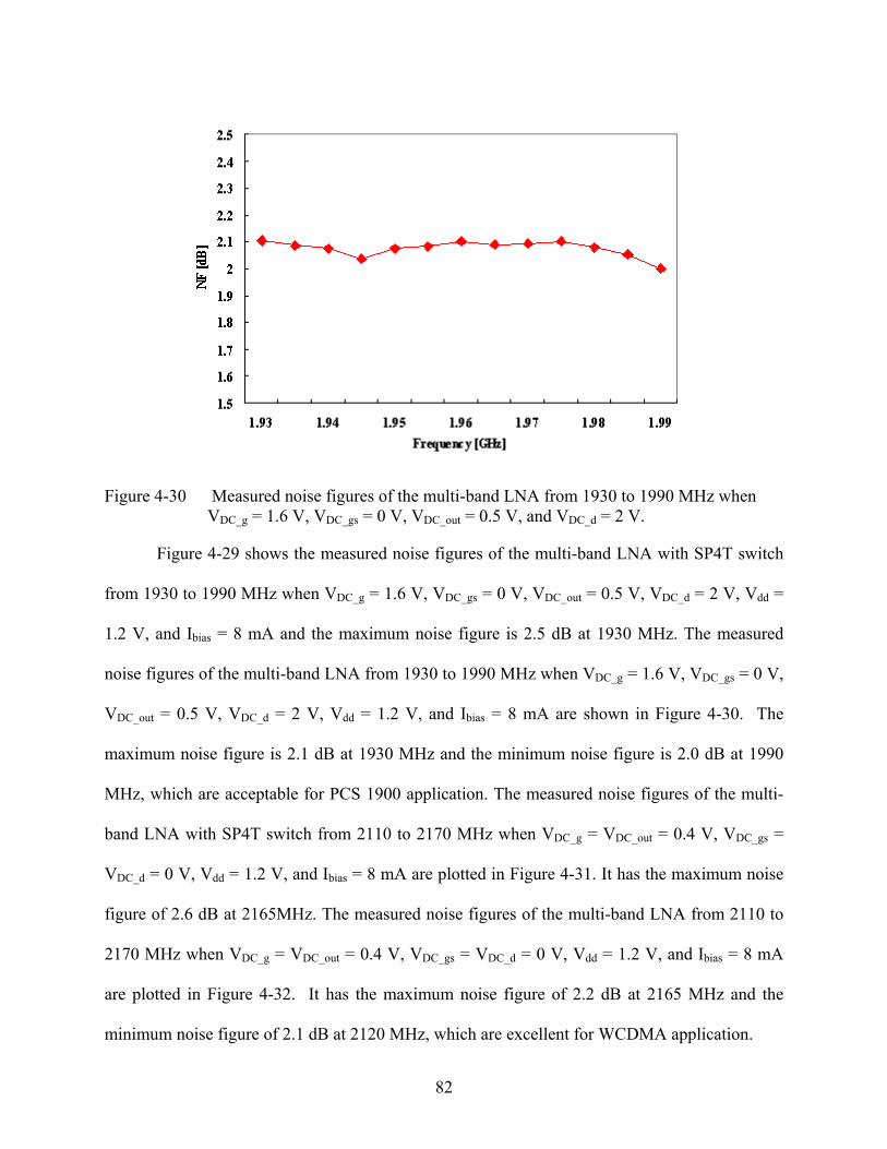
82
Figure 4-30 Measured noise figures of the multi-band LNA from 1930 to 1990 MHz when VDC_g = 1.6 V, VDC_gs = 0 V, VDC_out = 0.5 V, and VDC_d = 2 V.
Figure 4-29 shows the measured noise figures of the multi-band LNA with SP4T switch
from 1930 to 1990 MHz when VDC_g = 1.6 V, VDC_gs = 0 V, VDC_out = 0.5 V, VDC_d = 2 V, Vdd =
1.2 V, and Ibias = 8 mA and the maximum noise figure is 2.5 dB at 1930 MHz. The measured
noise figures of the multi-band LNA from 1930 to 1990 MHz when VDC_g = 1.6 V, VDC_gs = 0 V,
VDC_out = 0.5 V, VDC_d = 2 V, Vdd = 1.2 V, and Ibias = 8 mA are shown in Figure 4-30. The
maximum noise figure is 2.1 dB at 1930 MHz and the minimum noise figure is 2.0 dB at 1990
MHz, which are acceptable for PCS 1900 application. The measured noise figures of the multi-
band LNA with SP4T switch from 2110 to 2170 MHz when VDC_g = VDC_out = 0.4 V, VDC_gs =
VDC_d = 0 V, Vdd = 1.2 V, and Ibias = 8 mA are plotted in Figure 4-31. It has the maximum noise
figure of 2.6 dB at 2165MHz. The measured noise figures of the multi-band LNA from 2110 to
2170 MHz when VDC_g = VDC_out = 0.4 V, VDC_gs = VDC_d = 0 V, Vdd = 1.2 V, and Ibias = 8 mA
are plotted in Figure 4-32. It has the maximum noise figure of 2.2 dB at 2165 MHz and the
minimum noise figure of 2.1 dB at 2120 MHz, which are excellent for WCDMA application.
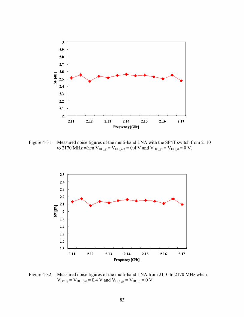
83
Figure 4-31 Measured noise figures of the multi-band LNA with the SP4T switch from 2110 to 2170 MHz when VDC_g = VDC_out = 0.4 V and VDC_gs = VDC_d = 0 V.
Figure 4-32 Measured noise figures of the multi-band LNA from 2110 to 2170 MHz when VDC_g = VDC_out = 0.4 V and VDC_gs = VDC_d = 0 V.
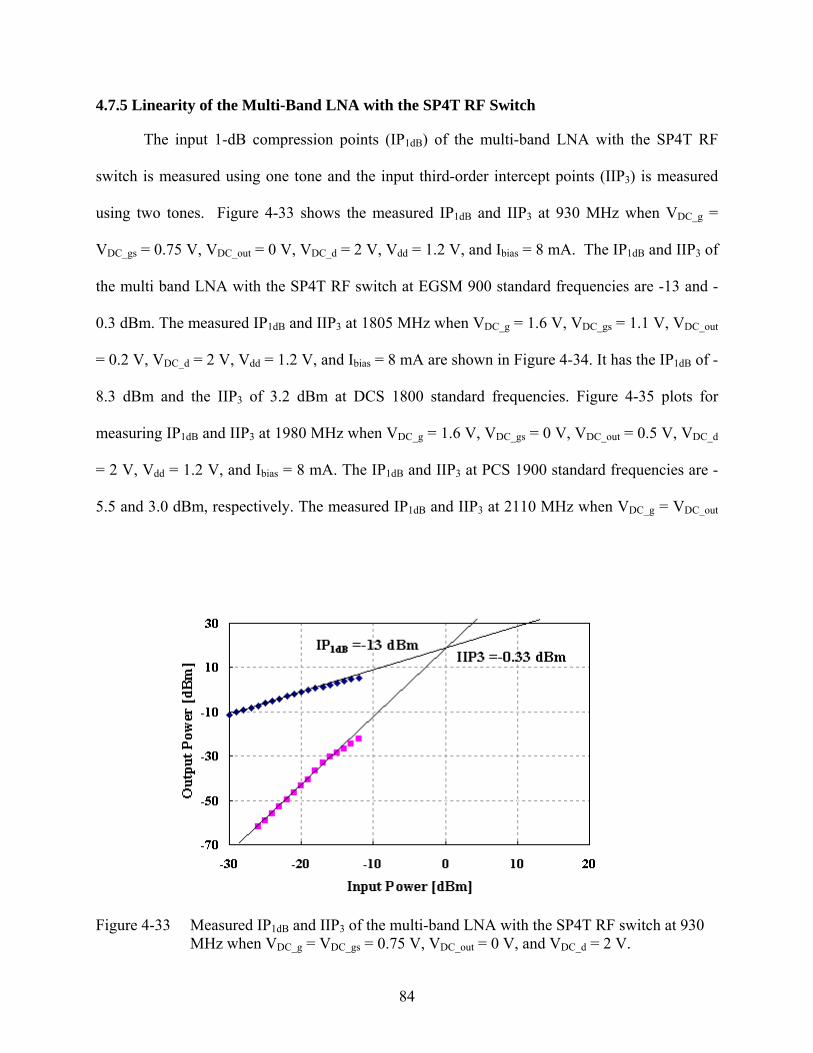
84
4.7.5 Linearity of the Multi-Band LNA with the SP4T RF Switch
The input 1-dB compression points (IP1dB) of the multi-band LNA with the SP4T RF
switch is measured using one tone and the input third-order intercept points (IIP3) is measured
using two tones. Figure 4-33 shows the measured IP1dB and IIP3 at 930 MHz when VDC_g =
VDC_gs = 0.75 V, VDC_out = 0 V, VDC_d = 2 V, Vdd = 1.2 V, and Ibias = 8 mA. The IP1dB and IIP3 of
the multi band LNA with the SP4T RF switch at EGSM 900 standard frequencies are -13 and -
0.3 dBm. The measured IP1dB and IIP3 at 1805 MHz when VDC_g = 1.6 V, VDC_gs = 1.1 V, VDC_out
= 0.2 V, VDC_d = 2 V, Vdd = 1.2 V, and Ibias = 8 mA are shown in Figure 4-34. It has the IP1dB of -
8.3 dBm and the IIP3 of 3.2 dBm at DCS 1800 standard frequencies. Figure 4-35 plots for
measuring IP1dB and IIP3 at 1980 MHz when VDC_g = 1.6 V, VDC_gs = 0 V, VDC_out = 0.5 V, VDC_d
= 2 V, Vdd = 1.2 V, and Ibias = 8 mA. The IP1dB and IIP3 at PCS 1900 standard frequencies are -
5.5 and 3.0 dBm, respectively. The measured IP1dB and IIP3 at 2110 MHz when VDC_g = VDC_out
Figure 4-33 Measured IP1dB and IIP3 of the multi-band LNA with the SP4T RF switch at 930 MHz when VDC_g = VDC_gs = 0.75 V, VDC_out = 0 V, and VDC_d = 2 V.
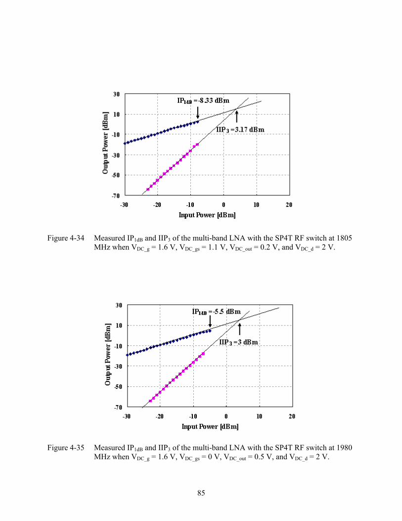
85
Figure 4-34 Measured IP1dB and IIP3 of the multi-band LNA with the SP4T RF switch at 1805 MHz when VDC_g = 1.6 V, VDC_gs = 1.1 V, VDC_out = 0.2 V, and VDC_d = 2 V.
Figure 4-35 Measured IP1dB and IIP3 of the multi-band LNA with the SP4T RF switch at 1980 MHz when VDC_g = 1.6 V, VDC_gs = 0 V, VDC_out = 0.5 V, and VDC_d = 2 V.
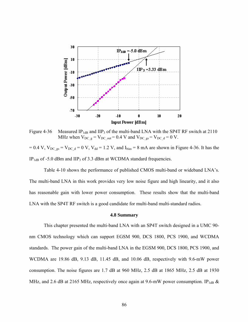
86
Figure 4-36 Measured IP1dB and IIP3 of the multi-band LNA with the SP4T RF switch at 2110
MHz when VDC_g = VDC_out = 0.4 V and VDC_gs = VDC_d = 0 V.
= 0.4 V, VDC_gs = VDC_d = 0 V, Vdd = 1.2 V, and Ibias = 8 mA are shown in Figure 4-36. It has the
IP1dB of -5.0 dBm and IIP3 of 3.3 dBm at WCDMA standard frequencies.
Table 4-10 shows the performance of published CMOS multi-band or wideband LNA’s.
The multi-band LNA in this work provides very low noise figure and high linearity, and it also
has reasonable gain with lower power consumption. These results show that the multi-band
LNA with the SP4T RF switch is a good candidate for multi-band multi-standard radios.
4.8 Summary
This chapter presented the multi-band LNA with an SP4T switch designed in a UMC 90-
nm CMOS technology which can support EGSM 900, DCS 1800, PCS 1900, and WCDMA
standards. The power gain of the multi-band LNA in the EGSM 900, DCS 1800, PCS 1900, and
WCDMA are 19.86 dB, 9.13 dB, 11.45 dB, and 10.06 dB, respectively with 9.6-mW power
consumption. The noise figures are 1.7 dB at 960 MHz, 2.5 dB at 1865 MHz, 2.5 dB at 1930
MHz, and 2.6 dB at 2165 MHz, respectively once again at 9.6-mW power consumption. IP1dB &
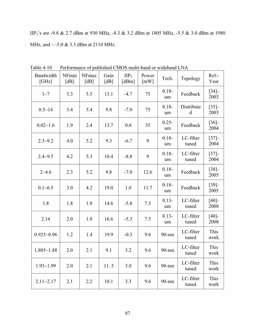
87
IIP3’s are -9.8 & 2.7 dBm at 930 MHz, -8.3 & 3.2 dBm at 1805 MHz, -5.5 & 3.0 dBm at 1980
MHz, and ~ -5.0 & 3.3 dBm at 2110 MHz.
Table 4-10 Performance of published CMOS multi-band or wideband LNA Bandwidth
[GHz] NFmin
[dB] NFmax
[dB] Gain [dB]
IIP3 [dBm]
Power [mW]
Tech. Topology Ref.-Year
1~7 3.3 5.5 13.1 -4.7 75 0.18-um Feedback [34]-
2003
0.5~14 3.4 5.4 9.8 -7.0 75 0.18-um
Distributed
[35]-2003
0.02~1.6 1.9 2.4 13.7 0.0 35 0.25-um Feedback [36]-
2004
2.3~9.2 4.0 5.2 9.3 -6.7 9 0.18-um
LC-filter tuned
[37]-2004
2.4~9.5 4.2 5.3 10.4 -8.8 9 0.18-um
LC-filter tuned
[37]-2004
2~4.6 2.3 5.2 9.8 -7.0 12.6 0.18-um Feedback [38]-
2005
0.1~6.5 3.0 4.2 19.0 1.0 11.7 0.18-um Feedback [39]-
2005
1.8 1.8 1.8 14.6 -5.8 7.5 0.13-um
LC-filter tuned
[40]-2008
2.14 2.0 1.8 16.6 -5.3 7.5 0.13-um
LC-filter tuned
[40]-2008
0.925~0.96 1.2 1.4 19.9 -0.3 9.6 90-nm LC-filter tuned
This work
1.805~1.88 2.0 2.1 9.1 3.2 9.6 90-nm LC-filter tuned
This work
1.93~1.99 2.0 2.1 11. 5 3.0 9.6 90-nm LC-filter tuned
This work
2.11~2.17 2.1 2.2 10.1 3.3 9.6 90-nm LC-filter tuned
This work
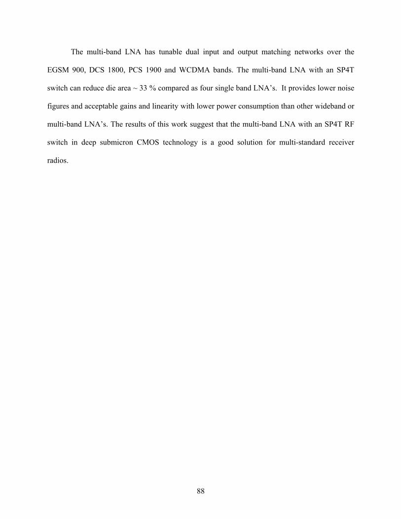
88
The multi-band LNA has tunable dual input and output matching networks over the
EGSM 900, DCS 1800, PCS 1900 and WCDMA bands. The multi-band LNA with an SP4T
switch can reduce die area ~ 33 % compared as four single band LNA’s. It provides lower noise
figures and acceptable gains and linearity with lower power consumption than other wideband or
multi-band LNA’s. The results of this work suggest that the multi-band LNA with an SP4T RF
switch in deep submicron CMOS technology is a good solution for multi-standard receiver
radios.
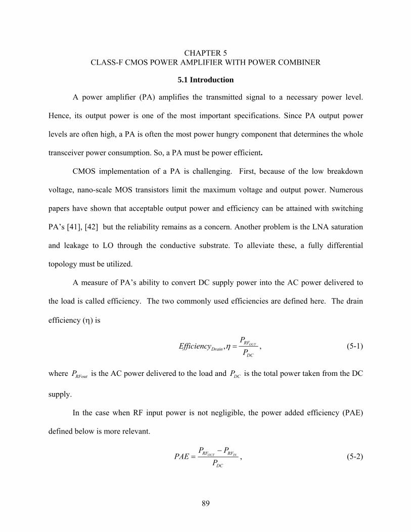
89
CHAPTER 5 CLASS-F CMOS POWER AMPLIFIER WITH POWER COMBINER
5.1 Introduction
A power amplifier (PA) amplifies the transmitted signal to a necessary power level.
Hence, its output power is one of the most important specifications. Since PA output power
levels are often high, a PA is often the most power hungry component that determines the whole
transceiver power consumption. So, a PA must be power efficient.
CMOS implementation of a PA is challenging. First, because of the low breakdown
voltage, nano-scale MOS transistors limit the maximum voltage and output power. Numerous
papers have shown that acceptable output power and efficiency can be attained with switching
PA’s [41], [42] but the reliability remains as a concern. Another problem is the LNA saturation
and leakage to LO through the conductive substrate. To alleviate these, a fully differential
topology must be utilized.
A measure of PA’s ability to convert DC supply power into the AC power delivered to
the load is called efficiency. The two commonly used efficiencies are defined here. The drain
efficiency (η) is
DC
RFDrain P
PEfficiency OUT=η, , (5-1)
where RFoutP is the AC power delivered to the load and DCP is the total power taken from the DC
supply.
In the case when RF input power is not negligible, the power added efficiency (PAE)
defined below is more relevant.
DC
RFRF
PPP
PAE INOUT−
= , (5-2)
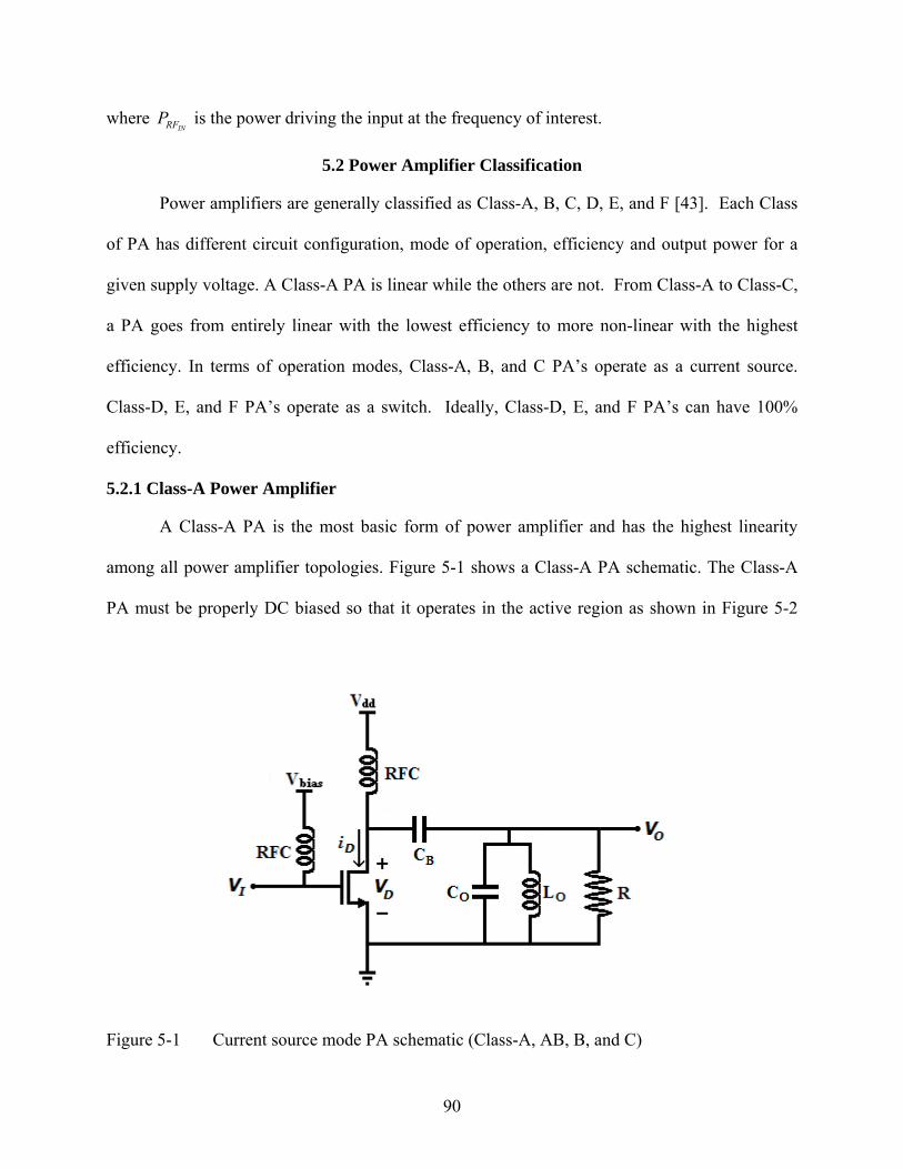
90
where INRFP is the power driving the input at the frequency of interest.
5.2 Power Amplifier Classification
Power amplifiers are generally classified as Class-A, B, C, D, E, and F [43]. Each Class
of PA has different circuit configuration, mode of operation, efficiency and output power for a
given supply voltage. A Class-A PA is linear while the others are not. From Class-A to Class-C,
a PA goes from entirely linear with the lowest efficiency to more non-linear with the highest
efficiency. In terms of operation modes, Class-A, B, and C PA’s operate as a current source.
Class-D, E, and F PA’s operate as a switch. Ideally, Class-D, E, and F PA’s can have 100%
efficiency.
5.2.1 Class-A Power Amplifier
A Class-A PA is the most basic form of power amplifier and has the highest linearity
among all power amplifier topologies. Figure 5-1 shows a Class-A PA schematic. The Class-A
PA must be properly DC biased so that it operates in the active region as shown in Figure 5-2
Figure 5-1 Current source mode PA schematic (Class-A, AB, B, and C)
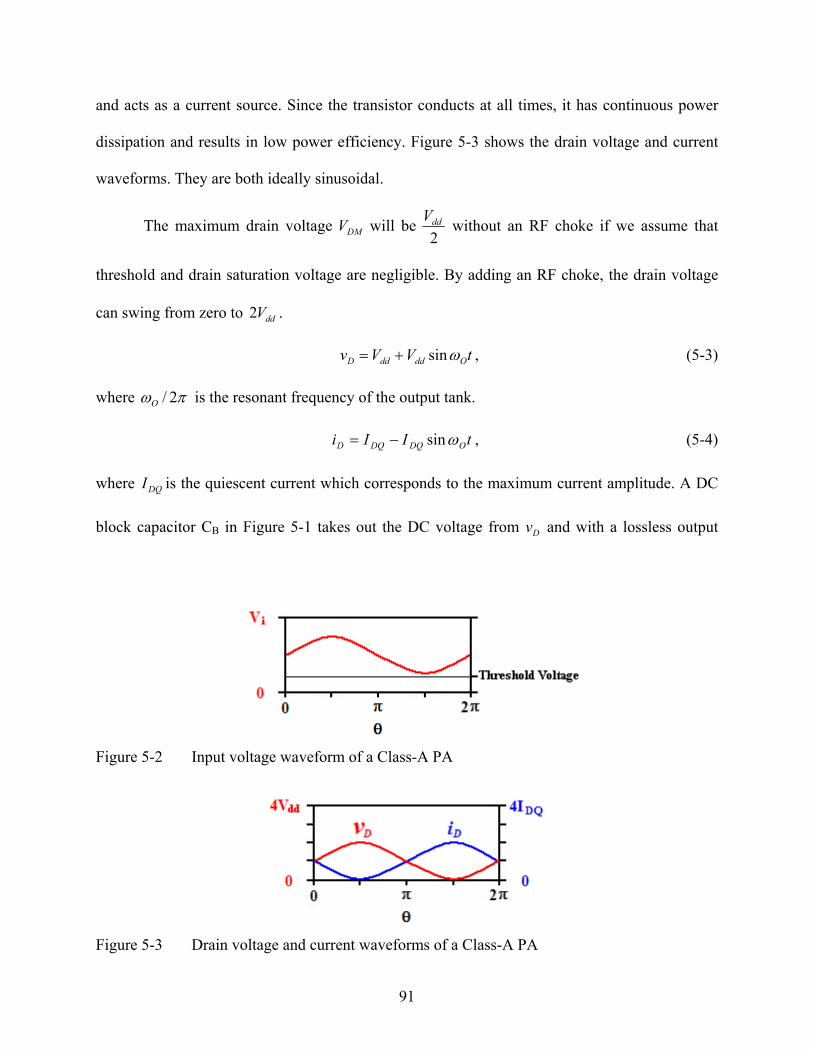
91
and acts as a current source. Since the transistor conducts at all times, it has continuous power
dissipation and results in low power efficiency. Figure 5-3 shows the drain voltage and current
waveforms. They are both ideally sinusoidal.
The maximum drain voltage DMV will be 2ddV without an RF choke if we assume that
threshold and drain saturation voltage are negligible. By adding an RF choke, the drain voltage
can swing from zero to ddV2 .
tVVv OddddD ωsin+= , (5-3)
where πω 2/O is the resonant frequency of the output tank.
tIIi ODQDQD ωsin−= , (5-4)
where DQI is the quiescent current which corresponds to the maximum current amplitude. A DC
block capacitor CB in Figure 5-1 takes out the DC voltage from Dv and with a lossless output
Figure 5-2 Input voltage waveform of a Class-A PA
Figure 5-3 Drain voltage and current waveforms of a Class-A PA
92
circuit, the output voltage at the load Ov is
tVv OddO ωsin= , (5-5)
The DC input power is
DQddDC IVP ⋅= , (5-6)
The RF output power is
2DQdd
RFout
IVP
⋅= , (5-7)
Hence, the maximum drain efficiency is
21
==DC
RFMAX P
POUTη . (5-8)
The ideal maximum drain efficiency of Class-A PA of 50% is not bad. However, the
efficiency of real Class-A PA’s is degraded by on-resistance and saturation voltage of the
transistor, and inductor power loss. The dissipated power is the difference between the DC input
power and RF output power.
RFoutDCnDissipatio PPP −= . (5-9)
5.2.2 Class-B Power Amplifier
A Class-B PA has the same schematic as a Class-A PA. However it must have gate DC
bias at the threshold of conduction so that it operates in the active region during half of the time
and drain current Di is a half sinusoid, which results in higher efficiency than that of the Class-A
PA. Figure 5-4 shows the drain voltage and current waveforms of Class-B PA. Here, the drain
voltage is ideally sinusoidal but the drain current is a half sinusoid.
Figure 5-5 shows a transformer coupled push-pull Class-B PA. During a positive half
cycle, one transistor pulls current from the load, and during a negative half cycle, the other
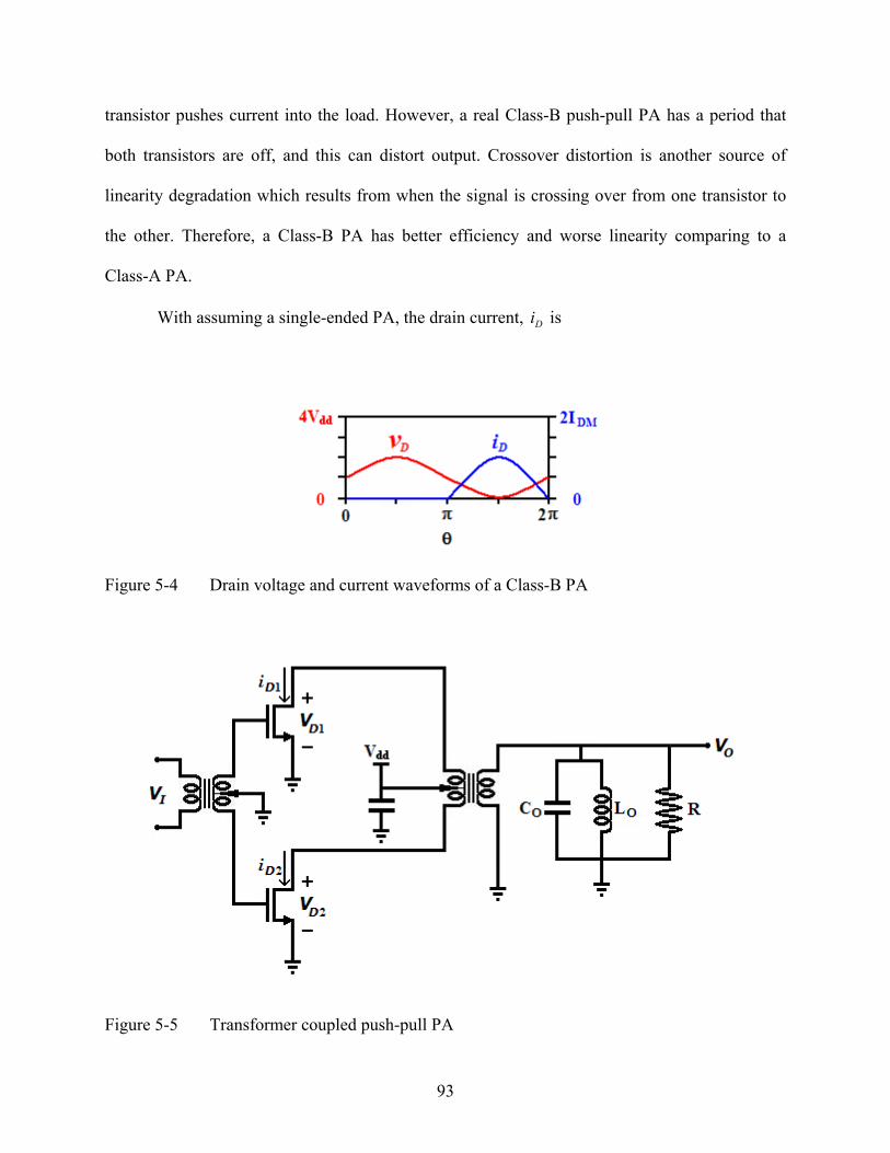
93
transistor pushes current into the load. However, a real Class-B push-pull PA has a period that
both transistors are off, and this can distort output. Crossover distortion is another source of
linearity degradation which results from when the signal is crossing over from one transistor to
the other. Therefore, a Class-B PA has better efficiency and worse linearity comparing to a
Class-A PA.
With assuming a single-ended PA, the drain current, Di is
Figure 5-4 Drain voltage and current waveforms of a Class-B PA
Figure 5-5 Transformer coupled push-pull PA
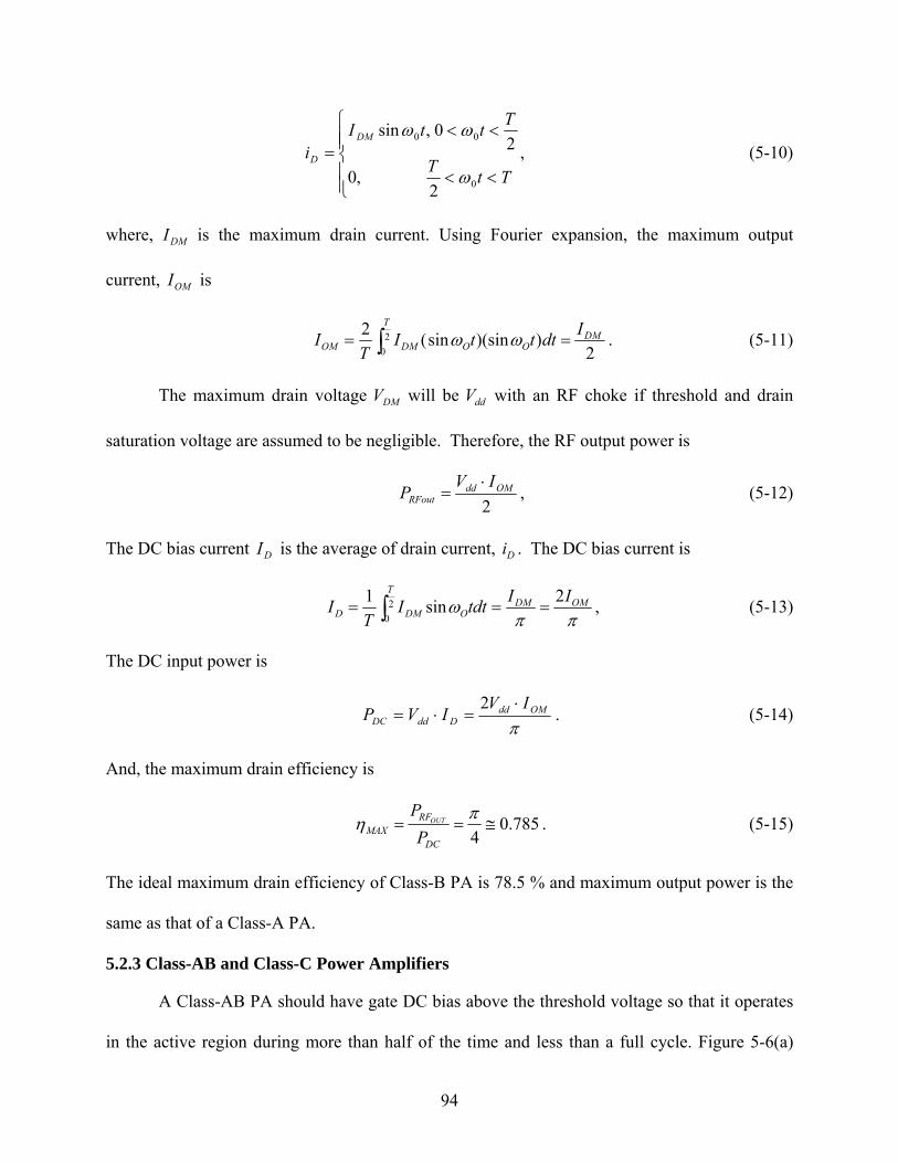
94
⎪⎪⎩
⎪⎪⎨
⎧
<<
<<=
TtT
TttIi
DM
D
0
00
2,0
20,sin
ω
ωω, (5-10)
where, DMI is the maximum drain current. Using Fourier expansion, the maximum output
current, OMI is
2))(sinsin(2 2
0DM
OO
T
DMOMIdtttI
TI == ∫ ωω . (5-11)
The maximum drain voltage DMV will be ddV with an RF choke if threshold and drain
saturation voltage are assumed to be negligible. Therefore, the RF output power is
2OMdd
RFoutIVP ⋅
= , (5-12)
The DC bias current DI is the average of drain current, Di . The DC bias current is
ππω OMDM
O
T
DMDIItdtI
TI 2sin1 2
0=== ∫ , (5-13)
The DC input power is
πOMdd
DddDCIV
IVP⋅
=⋅=2
. (5-14)
And, the maximum drain efficiency is
785.04≅==
πηDC
RFMAX P
POUT . (5-15)
The ideal maximum drain efficiency of Class-B PA is 78.5 % and maximum output power is the
same as that of a Class-A PA.
5.2.3 Class-AB and Class-C Power Amplifiers
A Class-AB PA should have gate DC bias above the threshold voltage so that it operates
in the active region during more than half of the time and less than a full cycle. Figure 5-6(a)
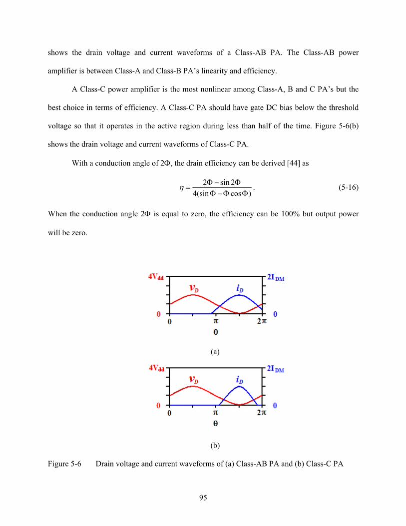
95
shows the drain voltage and current waveforms of a Class-AB PA. The Class-AB power
amplifier is between Class-A and Class-B PA’s linearity and efficiency.
A Class-C power amplifier is the most nonlinear among Class-A, B and C PA’s but the
best choice in terms of efficiency. A Class-C PA should have gate DC bias below the threshold
voltage so that it operates in the active region during less than half of the time. Figure 5-6(b)
shows the drain voltage and current waveforms of Class-C PA.
With a conduction angle of 2Φ, the drain efficiency can be derived [44] as
)cos(sin42sin2
ΦΦ−ΦΦ−Φ
=η . (5-16)
When the conduction angle 2Φ is equal to zero, the efficiency can be 100% but output power
will be zero.
(a)
(b)
Figure 5-6 Drain voltage and current waveforms of (a) Class-AB PA and (b) Class-C PA
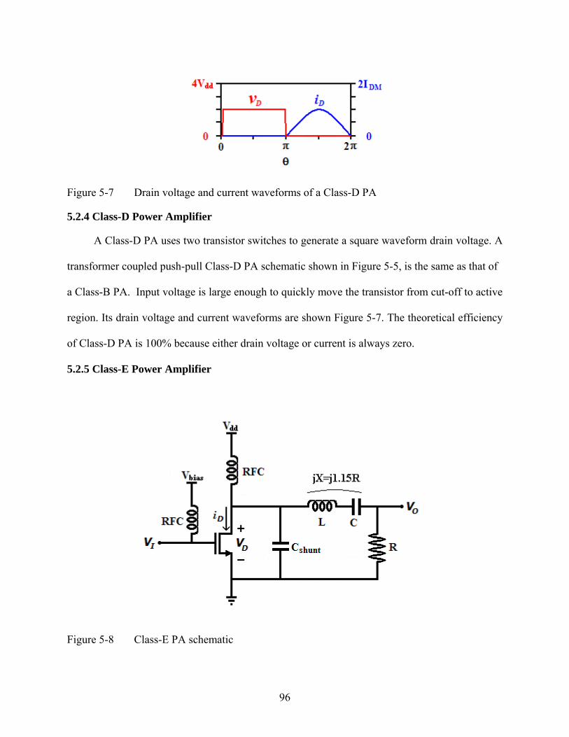
96
Figure 5-7 Drain voltage and current waveforms of a Class-D PA
5.2.4 Class-D Power Amplifier
A Class-D PA uses two transistor switches to generate a square waveform drain voltage. A
transformer coupled push-pull Class-D PA schematic shown in Figure 5-5, is the same as that of
a Class-B PA. Input voltage is large enough to quickly move the transistor from cut-off to active
region. Its drain voltage and current waveforms are shown Figure 5-7. The theoretical efficiency
of Class-D PA is 100% because either drain voltage or current is always zero.
5.2.5 Class-E Power Amplifier
Figure 5-8 Class-E PA schematic
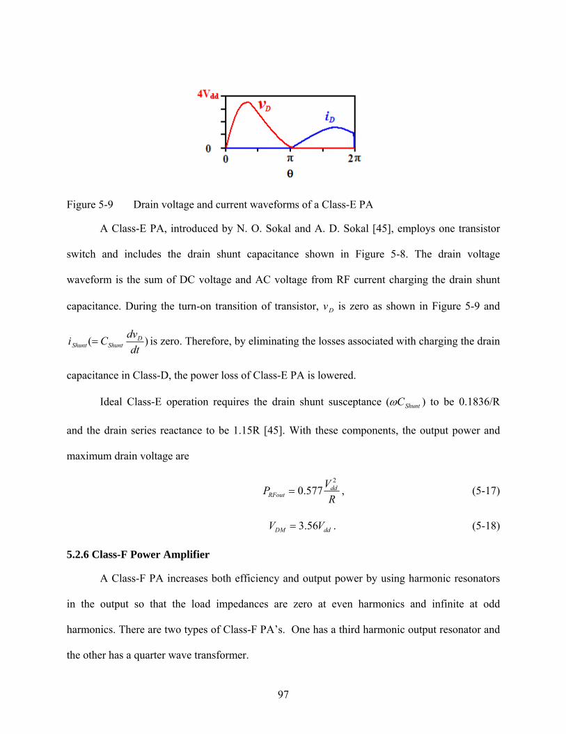
97
Figure 5-9 Drain voltage and current waveforms of a Class-E PA
A Class-E PA, introduced by N. O. Sokal and A. D. Sokal [45], employs one transistor
switch and includes the drain shunt capacitance shown in Figure 5-8. The drain voltage
waveform is the sum of DC voltage and AC voltage from RF current charging the drain shunt
capacitance. During the turn-on transition of transistor, Dv is zero as shown in Figure 5-9 and
)(dt
dvCi DShuntShunt = is zero. Therefore, by eliminating the losses associated with charging the drain
capacitance in Class-D, the power loss of Class-E PA is lowered.
Ideal Class-E operation requires the drain shunt susceptance )( ShuntCω to be 0.1836/R
and the drain series reactance to be 1.15R [45]. With these components, the output power and
maximum drain voltage are
RVP dd
RFout
2
577.0= , (5-17)
ddDM VV 56.3= . (5-18)
5.2.6 Class-F Power Amplifier
A Class-F PA increases both efficiency and output power by using harmonic resonators
in the output so that the load impedances are zero at even harmonics and infinite at odd
harmonics. There are two types of Class-F PA’s. One has a third harmonic output resonator and
the other has a quarter wave transformer.
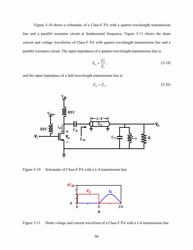
98
Figure 5-10 shows a schematic of a Class-F PA with a quarter-wavelength transmission
line and a parallel resonator circuit at fundamental frequency. Figure 5-11 shows the drain
current and voltage waveforms of Class-F PA with quarter-wavelength transmission line and a
parallel resonator circuit. The input impedance of a quarter-wavelength transmission line is
L
Oin Z
ZZ2
= , (5-19)
and the input impedance of a half-wavelength transmission line is
Lin ZZ = . (5-20)
Figure 5-10 Schematic of Class-F PA with a λ/4 transmission line
Figure 5-11 Drain voltage and current waveform of a Class-F PA with a λ/4 transmission line
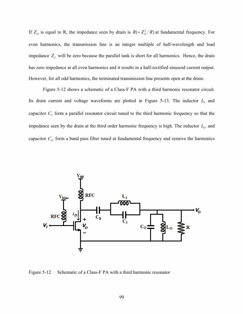
99
If OZ is equal to R, the impedance seen by drain is )/( 2 RZR O= at fundamental frequency. For
even harmonics, the transmission line is an integer multiple of half-wavelength and load
impedance LZ will be zero because the parallel tank is short for all harmonics. Hence, the drain
has zero impedance at all even harmonics and it results in a half-rectified sinusoid current output.
However, for all odd harmonics, the terminated transmission line presents open at the drain.
Figure 5-12 shows a schematic of a Class-F PA with a third harmonic resonator circuit.
Its drain current and voltage waveforms are plotted in Figure 5-13. The inductor 3L and
capacitor 3C form a parallel resonator circuit tuned to the third harmonic frequency so that the
impedance seen by the drain at the third order harmonic frequency is high. The inductor OL and
capacitor OC form a band pass filter tuned at fundamental frequency and remove the harmonics
Figure 5-12 Schematic of a Class-F PA with a third harmonic resonator
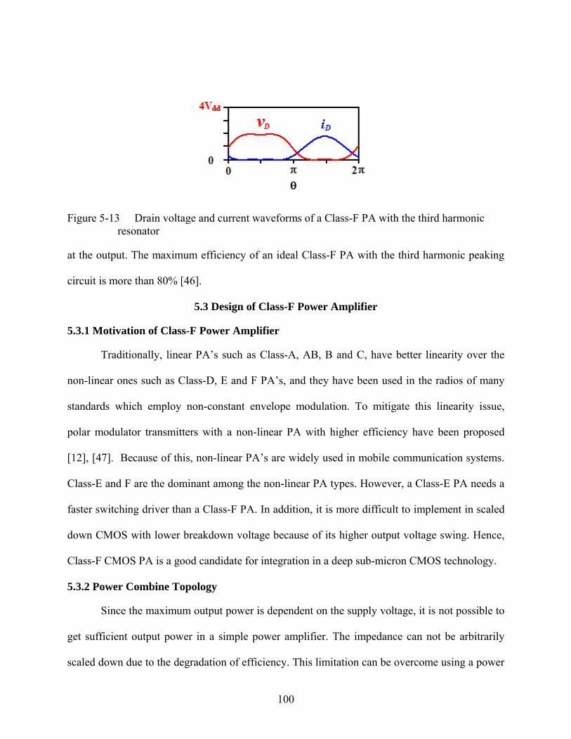
100
Figure 5-13 Drain voltage and current waveforms of a Class-F PA with the third harmonic resonator
at the output. The maximum efficiency of an ideal Class-F PA with the third harmonic peaking
circuit is more than 80% [46].
5.3 Design of Class-F Power Amplifier
5.3.1 Motivation of Class-F Power Amplifier
Traditionally, linear PA’s such as Class-A, AB, B and C, have better linearity over the
non-linear ones such as Class-D, E and F PA’s, and they have been used in the radios of many
standards which employ non-constant envelope modulation. To mitigate this linearity issue,
polar modulator transmitters with a non-linear PA with higher efficiency have been proposed
[12], [47]. Because of this, non-linear PA’s are widely used in mobile communication systems.
Class-E and F are the dominant among the non-linear PA types. However, a Class-E PA needs a
faster switching driver than a Class-F PA. In addition, it is more difficult to implement in scaled
down CMOS with lower breakdown voltage because of its higher output voltage swing. Hence,
Class-F CMOS PA is a good candidate for integration in a deep sub-micron CMOS technology.
5.3.2 Power Combine Topology
Since the maximum output power is dependent on the supply voltage, it is not possible to
get sufficient output power in a simple power amplifier. The impedance can not be arbitrarily
scaled down due to the degradation of efficiency. This limitation can be overcome using a power
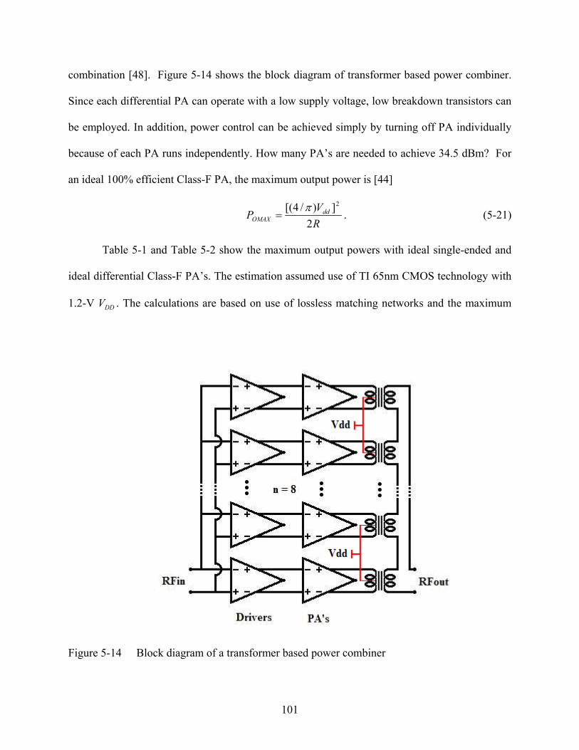
101
combination [48]. Figure 5-14 shows the block diagram of transformer based power combiner.
Since each differential PA can operate with a low supply voltage, low breakdown transistors can
be employed. In addition, power control can be achieved simply by turning off PA individually
because of each PA runs independently. How many PA’s are needed to achieve 34.5 dBm? For
an ideal 100% efficient Class-F PA, the maximum output power is [44]
RV
P ddOMAX 2
])/4[( 2π= . (5-21)
Table 5-1 and Table 5-2 show the maximum output powers with ideal single-ended and
ideal differential Class-F PA’s. The estimation assumed use of TI 65nm CMOS technology with
1.2-V DDV . The calculations are based on use of lossless matching networks and the maximum
Figure 5-14 Block diagram of a transformer based power combiner
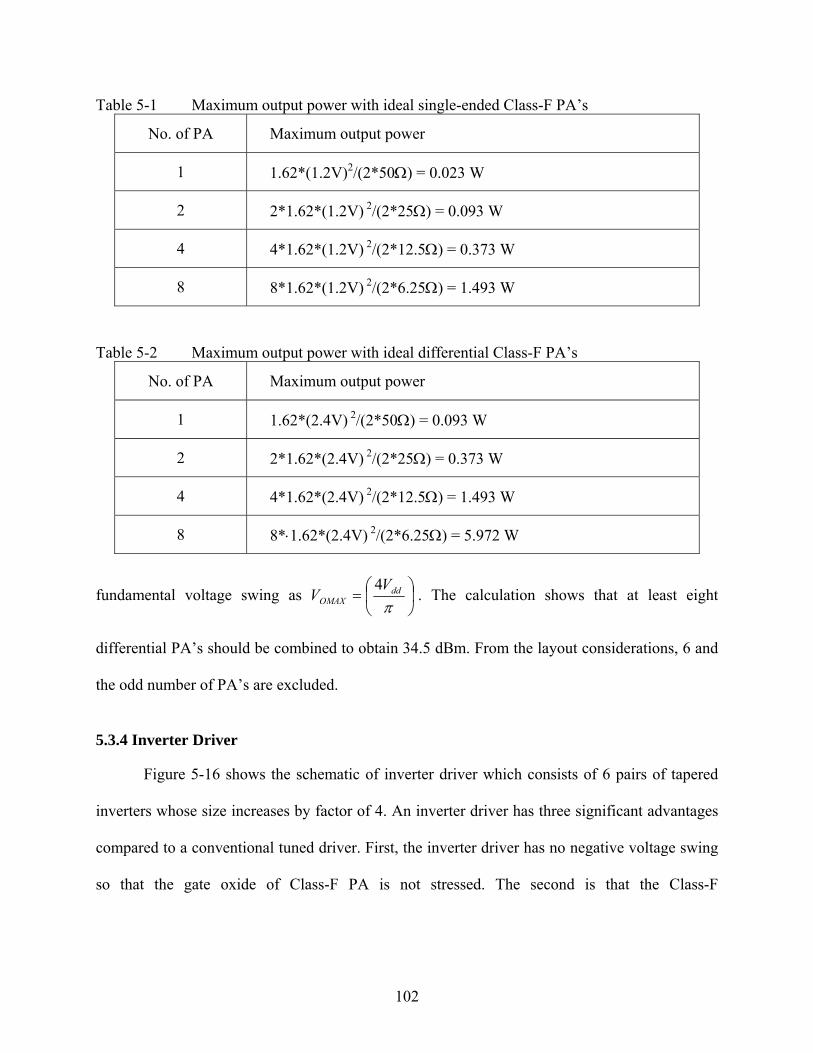
102
Table 5-1 Maximum output power with ideal single-ended Class-F PA’s
No. of PA Maximum output power
1 1.62*(1.2V)2/(2*50Ω) = 0.023 W
2 2*1.62*(1.2V) 2/(2*25Ω) = 0.093 W
4 4*1.62*(1.2V) 2/(2*12.5Ω) = 0.373 W
8 8*1.62*(1.2V) 2/(2*6.25Ω) = 1.493 W
Table 5-2 Maximum output power with ideal differential Class-F PA’s
No. of PA Maximum output power
1 1.62*(2.4V) 2/(2*50Ω) = 0.093 W
2 2*1.62*(2.4V) 2/(2*25Ω) = 0.373 W
4 4*1.62*(2.4V) 2/(2*12.5Ω) = 1.493 W
8 8*⋅1.62*(2.4V) 2/(2*6.25Ω) = 5.972 W
fundamental voltage swing as ⎟⎠⎞
⎜⎝⎛=
πdd
OMAXV
V4
. The calculation shows that at least eight
differential PA’s should be combined to obtain 34.5 dBm. From the layout considerations, 6 and
the odd number of PA’s are excluded.
5.3.4 Inverter Driver
Figure 5-16 shows the schematic of inverter driver which consists of 6 pairs of tapered
inverters whose size increases by factor of 4. An inverter driver has three significant advantages
compared to a conventional tuned driver. First, the inverter driver has no negative voltage swing
so that the gate oxide of Class-F PA is not stressed. The second is that the Class-F
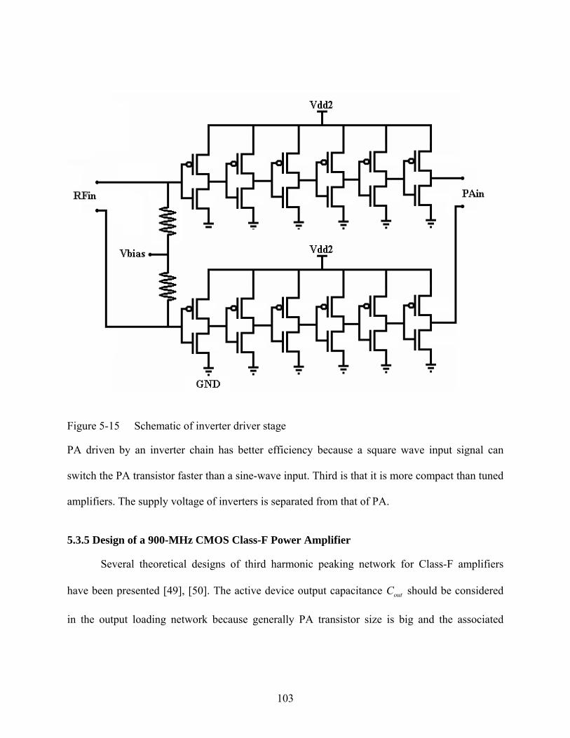
103
Figure 5-15 Schematic of inverter driver stage
PA driven by an inverter chain has better efficiency because a square wave input signal can
switch the PA transistor faster than a sine-wave input. Third is that it is more compact than tuned
amplifiers. The supply voltage of inverters is separated from that of PA.
5.3.5 Design of a 900-MHz CMOS Class-F Power Amplifier
Several theoretical designs of third harmonic peaking network for Class-F amplifiers
have been presented [49], [50]. The active device output capacitance outC should be considered
in the output loading network because generally PA transistor size is big and the associated
104
(a) (b)
Figure 5-16 Third harmonic peaking load networks of Class-F PA’s with additional (a) series
resonant circuit and (b) parallel resonant circuit
parasitic capacitance is not negligible. Figure 5-16 shows two possible third harmonic peaking
load networks with additional (a) series resonant circuit and (b) parallel resonant circuit.
The 1L , 2L , and 2C in Figure 5-16(a) are
1615
,159
,9
42
121
out
outo
CC
LL
CL ===
ω, (5-22)
where πω 2/O is the resonant frequency of the output tank.
The 1L , 2L , and 2C in Figure 5-16(b) are
512
,3
5,6
12
121
out
outo
CCLL
CL ===
ω. (5-23)
In this PA design, the topology in Figure 5-16(a) is chosen and Equation (5-22) is a good starting
point for design.
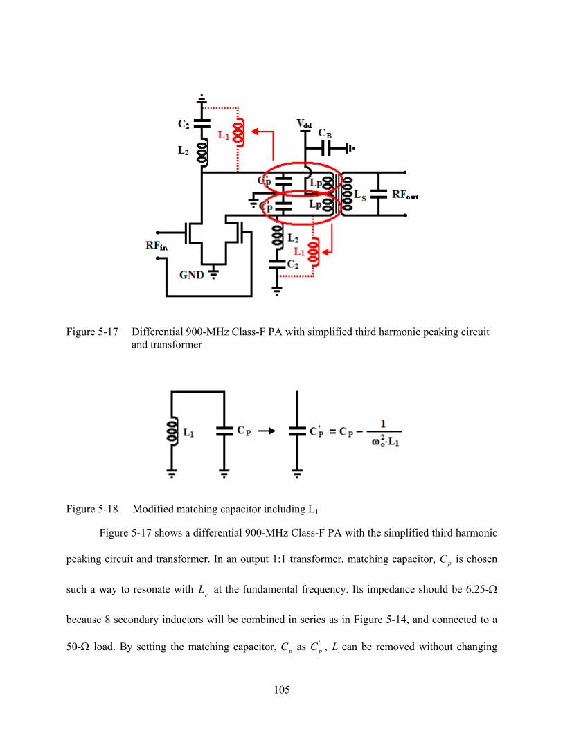
105
Figure 5-17 Differential 900-MHz Class-F PA with simplified third harmonic peaking circuit and transformer
Figure 5-18 Modified matching capacitor including L1
Figure 5-17 shows a differential 900-MHz Class-F PA with the simplified third harmonic
peaking circuit and transformer. In an output 1:1 transformer, matching capacitor, pC is chosen
such a way to resonate with pL at the fundamental frequency. Its impedance should be 6.25-Ω
because 8 secondary inductors will be combined in series as in Figure 5-14, and connected to a
50-Ω load. By setting the matching capacitor, pC as 'pC , 1L can be removed without changing
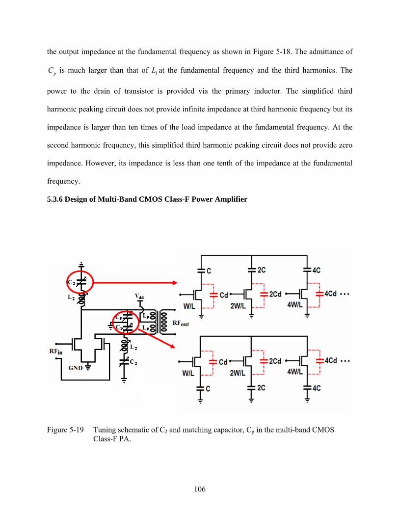
106
the output impedance at the fundamental frequency as shown in Figure 5-18. The admittance of
pC is much larger than that of 1L at the fundamental frequency and the third harmonics. The
power to the drain of transistor is provided via the primary inductor. The simplified third
harmonic peaking circuit does not provide infinite impedance at third harmonic frequency but its
impedance is larger than ten times of the load impedance at the fundamental frequency. At the
second harmonic frequency, this simplified third harmonic peaking circuit does not provide zero
impedance. However, its impedance is less than one tenth of the impedance at the fundamental
frequency.
5.3.6 Design of Multi-Band CMOS Class-F Power Amplifier
Figure 5-19 Tuning schematic of C2 and matching capacitor, Cp in the multi-band CMOS Class-F PA.
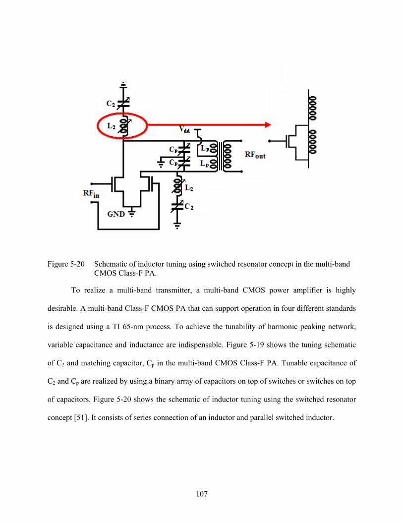
107
Figure 5-20 Schematic of inductor tuning using switched resonator concept in the multi-band CMOS Class-F PA.
To realize a multi-band transmitter, a multi-band CMOS power amplifier is highly
desirable. A multi-band Class-F CMOS PA that can support operation in four different standards
is designed using a TI 65-nm process. To achieve the tunability of harmonic peaking network,
variable capacitance and inductance are indispensable. Figure 5-19 shows the tuning schematic
of C2 and matching capacitor, Cp in the multi-band CMOS Class-F PA. Tunable capacitance of
C2 and Cp are realized by using a binary array of capacitors on top of switches or switches on top
of capacitors. Figure 5-20 shows the schematic of inductor tuning using the switched resonator
concept [51]. It consists of series connection of an inductor and parallel switched inductor.
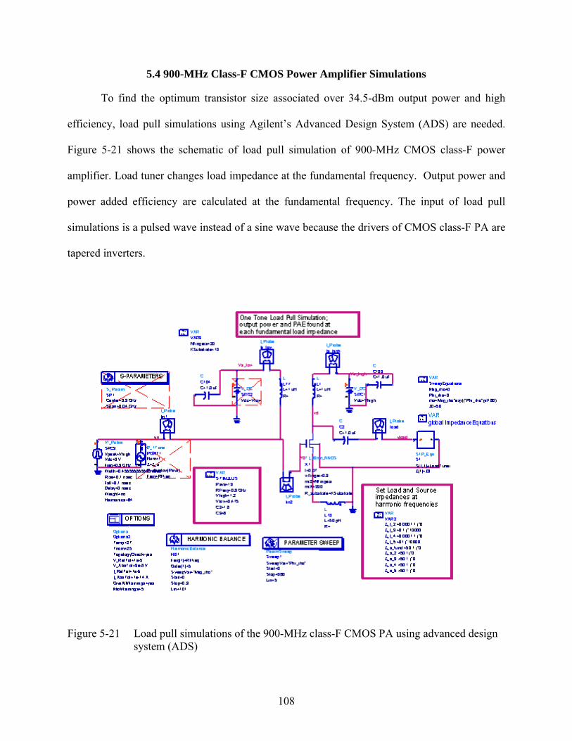
108
5.4 900-MHz Class-F CMOS Power Amplifier Simulations
To find the optimum transistor size associated over 34.5-dBm output power and high
efficiency, load pull simulations using Agilent’s Advanced Design System (ADS) are needed.
Figure 5-21 shows the schematic of load pull simulation of 900-MHz CMOS class-F power
amplifier. Load tuner changes load impedance at the fundamental frequency. Output power and
power added efficiency are calculated at the fundamental frequency. The input of load pull
simulations is a pulsed wave instead of a sine wave because the drivers of CMOS class-F PA are
tapered inverters.
Figure 5-21 Load pull simulations of the 900-MHz class-F CMOS PA using advanced design
system (ADS)
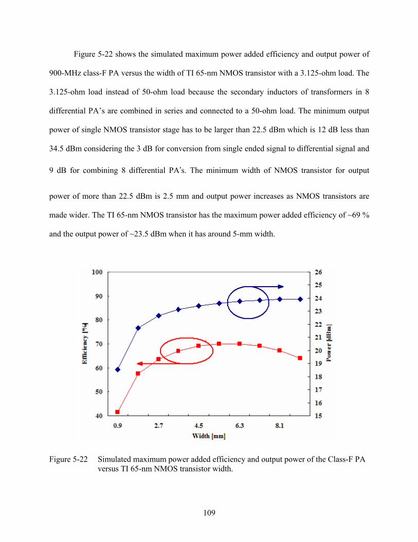
109
Figure 5-22 shows the simulated maximum power added efficiency and output power of
900-MHz class-F PA versus the width of TI 65-nm NMOS transistor with a 3.125-ohm load. The
3.125-ohm load instead of 50-ohm load because the secondary inductors of transformers in 8
differential PA’s are combined in series and connected to a 50-ohm load. The minimum output
power of single NMOS transistor stage has to be larger than 22.5 dBm which is 12 dB less than
34.5 dBm considering the 3 dB for conversion from single ended signal to differential signal and
9 dB for combining 8 differential PA’s. The minimum width of NMOS transistor for output
power of more than 22.5 dBm is 2.5 mm and output power increases as NMOS transistors are
made wider. The TI 65-nm NMOS transistor has the maximum power added efficiency of ~69 %
and the output power of ~23.5 dBm when it has around 5-mm width.
Figure 5-22 Simulated maximum power added efficiency and output power of the Class-F PA versus TI 65-nm NMOS transistor width.
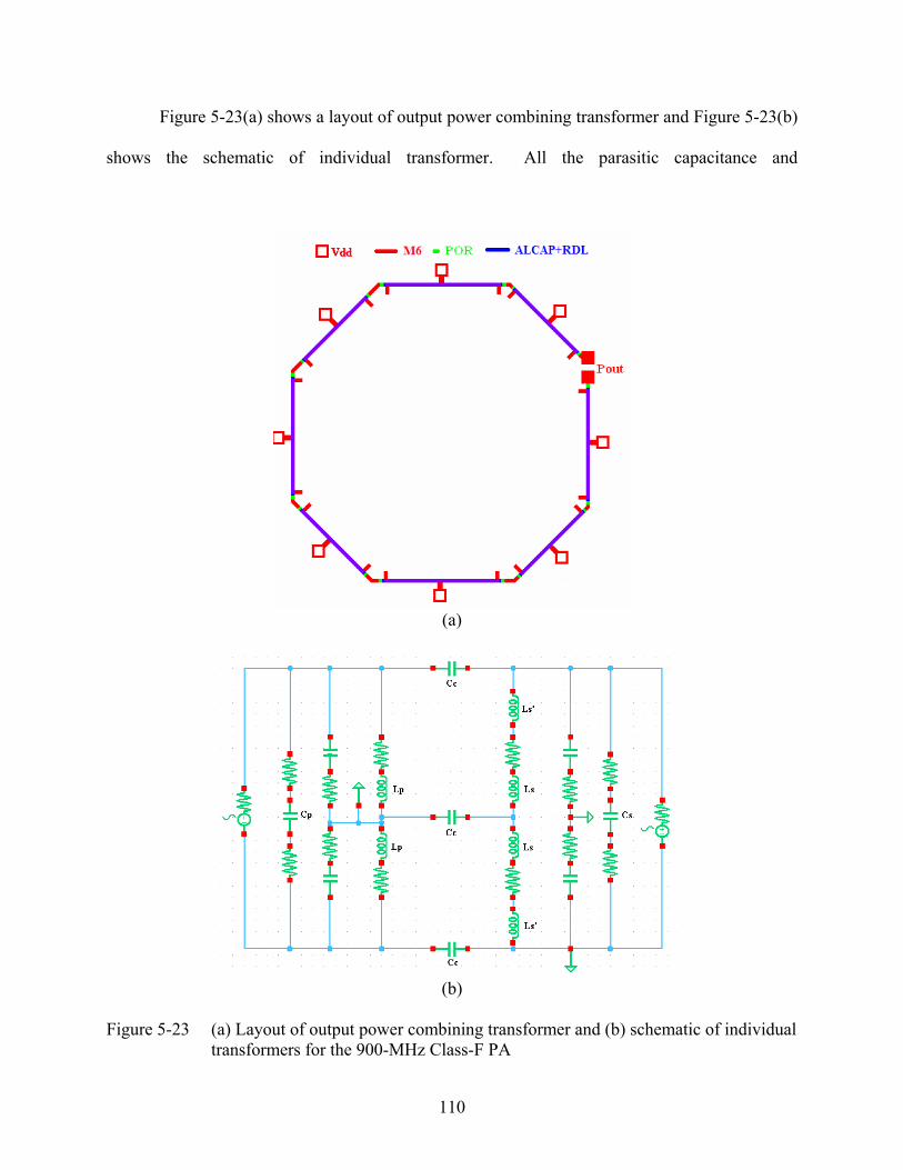
110
Figure 5-23(a) shows a layout of output power combining transformer and Figure 5-23(b)
shows the schematic of individual transformer. All the parasitic capacitance and
(a)
(b)
Figure 5-23 (a) Layout of output power combining transformer and (b) schematic of individual
transformers for the 900-MHz Class-F PA
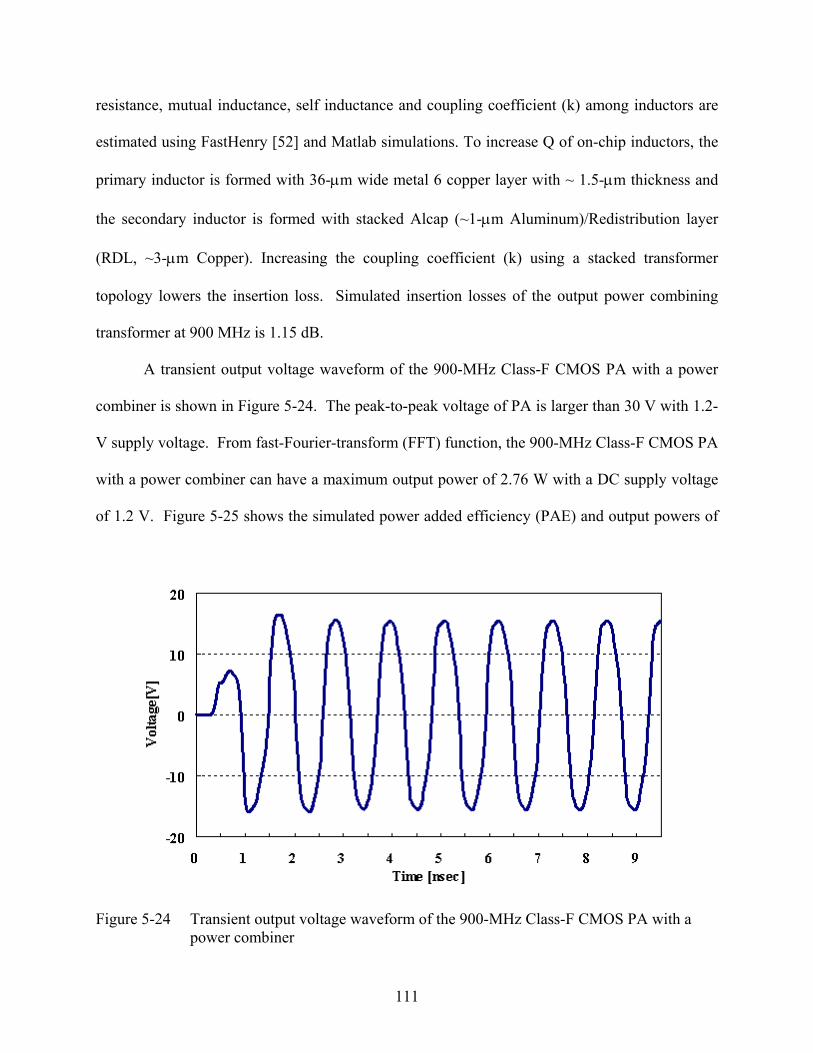
111
resistance, mutual inductance, self inductance and coupling coefficient (k) among inductors are
estimated using FastHenry [52] and Matlab simulations. To increase Q of on-chip inductors, the
primary inductor is formed with 36-μm wide metal 6 copper layer with ~ 1.5-μm thickness and
the secondary inductor is formed with stacked Alcap (~1-μm Aluminum)/Redistribution layer
(RDL, ~3-μm Copper). Increasing the coupling coefficient (k) using a stacked transformer
topology lowers the insertion loss. Simulated insertion losses of the output power combining
transformer at 900 MHz is 1.15 dB.
A transient output voltage waveform of the 900-MHz Class-F CMOS PA with a power
combiner is shown in Figure 5-24. The peak-to-peak voltage of PA is larger than 30 V with 1.2-
V supply voltage. From fast-Fourier-transform (FFT) function, the 900-MHz Class-F CMOS PA
with a power combiner can have a maximum output power of 2.76 W with a DC supply voltage
of 1.2 V. Figure 5-25 shows the simulated power added efficiency (PAE) and output powers of
Figure 5-24 Transient output voltage waveform of the 900-MHz Class-F CMOS PA with a power combiner
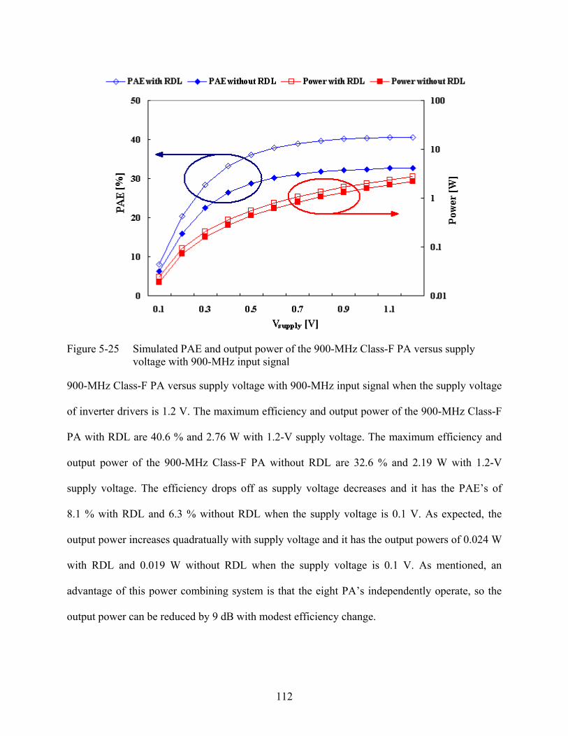
112
Figure 5-25 Simulated PAE and output power of the 900-MHz Class-F PA versus supply
voltage with 900-MHz input signal
900-MHz Class-F PA versus supply voltage with 900-MHz input signal when the supply voltage
of inverter drivers is 1.2 V. The maximum efficiency and output power of the 900-MHz Class-F
PA with RDL are 40.6 % and 2.76 W with 1.2-V supply voltage. The maximum efficiency and
output power of the 900-MHz Class-F PA without RDL are 32.6 % and 2.19 W with 1.2-V
supply voltage. The efficiency drops off as supply voltage decreases and it has the PAE’s of
8.1 % with RDL and 6.3 % without RDL when the supply voltage is 0.1 V. As expected, the
output power increases quadratually with supply voltage and it has the output powers of 0.024 W
with RDL and 0.019 W without RDL when the supply voltage is 0.1 V. As mentioned, an
advantage of this power combining system is that the eight PA’s independently operate, so the
output power can be reduced by 9 dB with modest efficiency change.
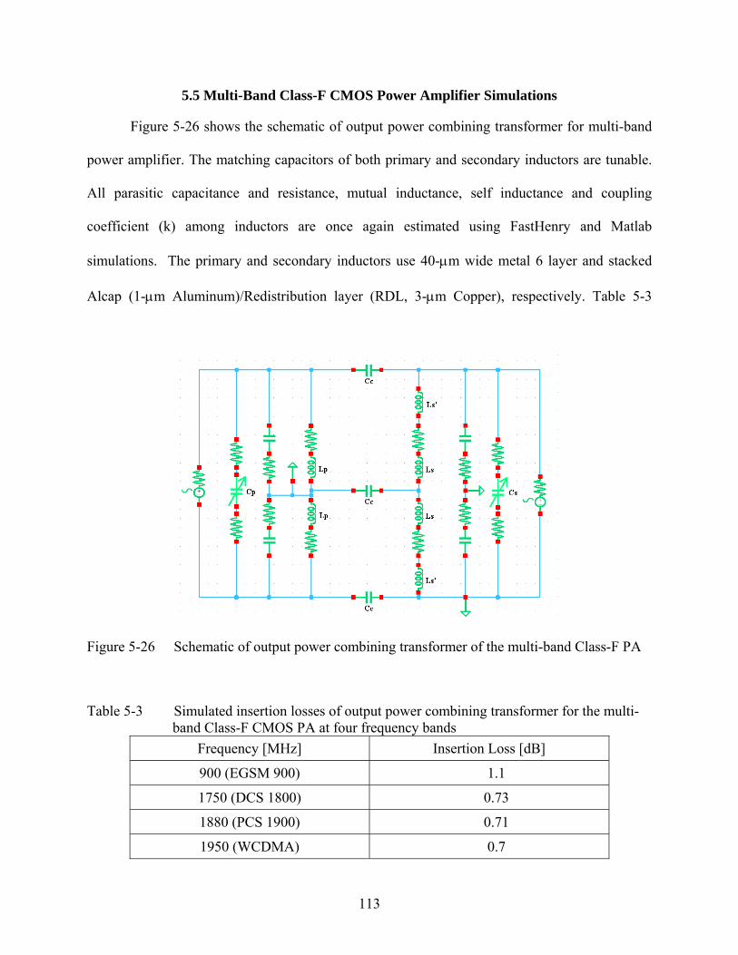
113
5.5 Multi-Band Class-F CMOS Power Amplifier Simulations
Figure 5-26 shows the schematic of output power combining transformer for multi-band
power amplifier. The matching capacitors of both primary and secondary inductors are tunable.
All parasitic capacitance and resistance, mutual inductance, self inductance and coupling
coefficient (k) among inductors are once again estimated using FastHenry and Matlab
simulations. The primary and secondary inductors use 40-μm wide metal 6 layer and stacked
Alcap (1-μm Aluminum)/Redistribution layer (RDL, 3-μm Copper), respectively. Table 5-3
Figure 5-26 Schematic of output power combining transformer of the multi-band Class-F PA
Table 5-3 Simulated insertion losses of output power combining transformer for the multi-band Class-F CMOS PA at four frequency bands
Frequency [MHz] Insertion Loss [dB]
900 (EGSM 900) 1.1
1750 (DCS 1800) 0.73
1880 (PCS 1900) 0.71
1950 (WCDMA) 0.7
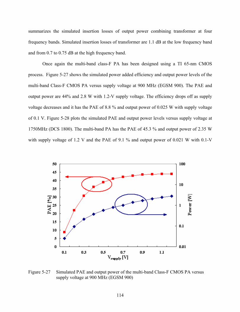
114
summarizes the simulated insertion losses of output power combining transformer at four
frequency bands. Simulated insertion losses of transformer are 1.1 dB at the low frequency band
and from 0.7 to 0.75 dB at the high frequency band.
Once again the multi-band class-F PA has been designed using a TI 65-nm CMOS
process. Figure 5-27 shows the simulated power added efficiency and output power levels of the
multi-band Class-F CMOS PA versus supply voltage at 900 MHz (EGSM 900). The PAE and
output power are 44% and 2.8 W with 1.2-V supply voltage. The efficiency drops off as supply
voltage decreases and it has the PAE of 8.8 % and output power of 0.025 W with supply voltage
of 0.1 V. Figure 5-28 plots the simulated PAE and output power levels versus supply voltage at
1750MHz (DCS 1800). The multi-band PA has the PAE of 45.3 % and output power of 2.35 W
with supply voltage of 1.2 V and the PAE of 9.1 % and output power of 0.021 W with 0.1-V
Figure 5-27 Simulated PAE and output power of the multi-band Class-F CMOS PA versus supply voltage at 900 MHz (EGSM 900)
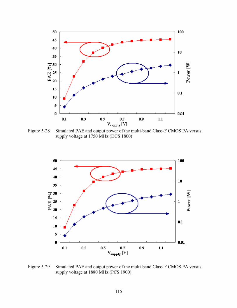
115
Figure 5-28 Simulated PAE and output power of the multi-band Class-F CMOS PA versus
supply voltage at 1750 MHz (DCS 1800)
Figure 5-29 Simulated PAE and output power of the multi-band Class-F CMOS PA versus supply voltage at 1880 MHz (PCS 1900)
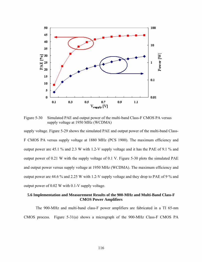
116
Figure 5-30 Simulated PAE and output power of the multi-band Class-F CMOS PA versus supply voltage at 1950 MHz (WCDMA)
supply voltage. Figure 5-29 shows the simulated PAE and output power of the multi-band Class-
F CMOS PA versus supply voltage at 1880 MHz (PCS 1900). The maximum efficiency and
output power are 45.1 % and 2.3 W with 1.2-V supply voltage and it has the PAE of 9.1 % and
output power of 0.21 W with the supply voltage of 0.1 V. Figure 5-30 plots the simulated PAE
and output power versus supply voltage at 1950 MHz (WCDMA). The maximum efficiency and
output power are 44.6 % and 2.25 W with 1.2-V supply voltage and they drop to PAE of 9 % and
output power of 0.02 W with 0.1-V supply voltage.
5.6 Implementation and Measurement Results of the 900-MHz and Multi-Band Class-F CMOS Power Amplifiers
The 900-MHz and multi-band class-F power amplifiers are fabricated in a TI 65-nm
CMOS process. Figure 5-31(a) shows a micrograph of the 900-MHz Class-F CMOS PA
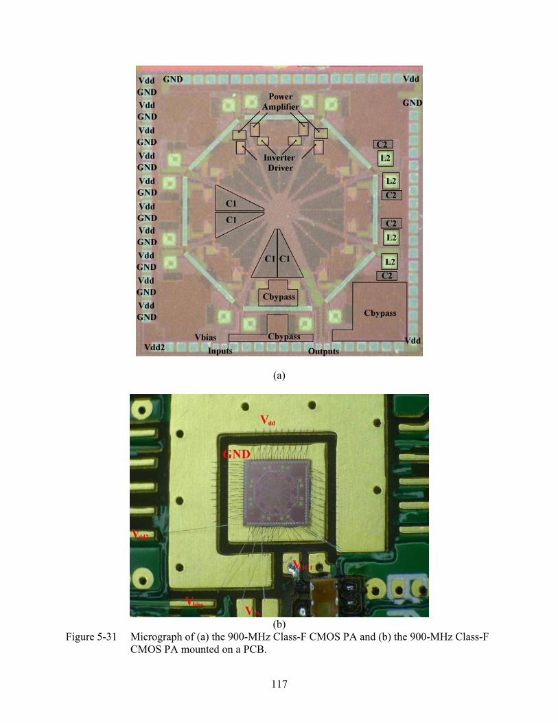
117
(a)
(b)
Figure 5-31 Micrograph of (a) the 900-MHz Class-F CMOS PA and (b) the 900-MHz Class-F CMOS PA mounted on a PCB.
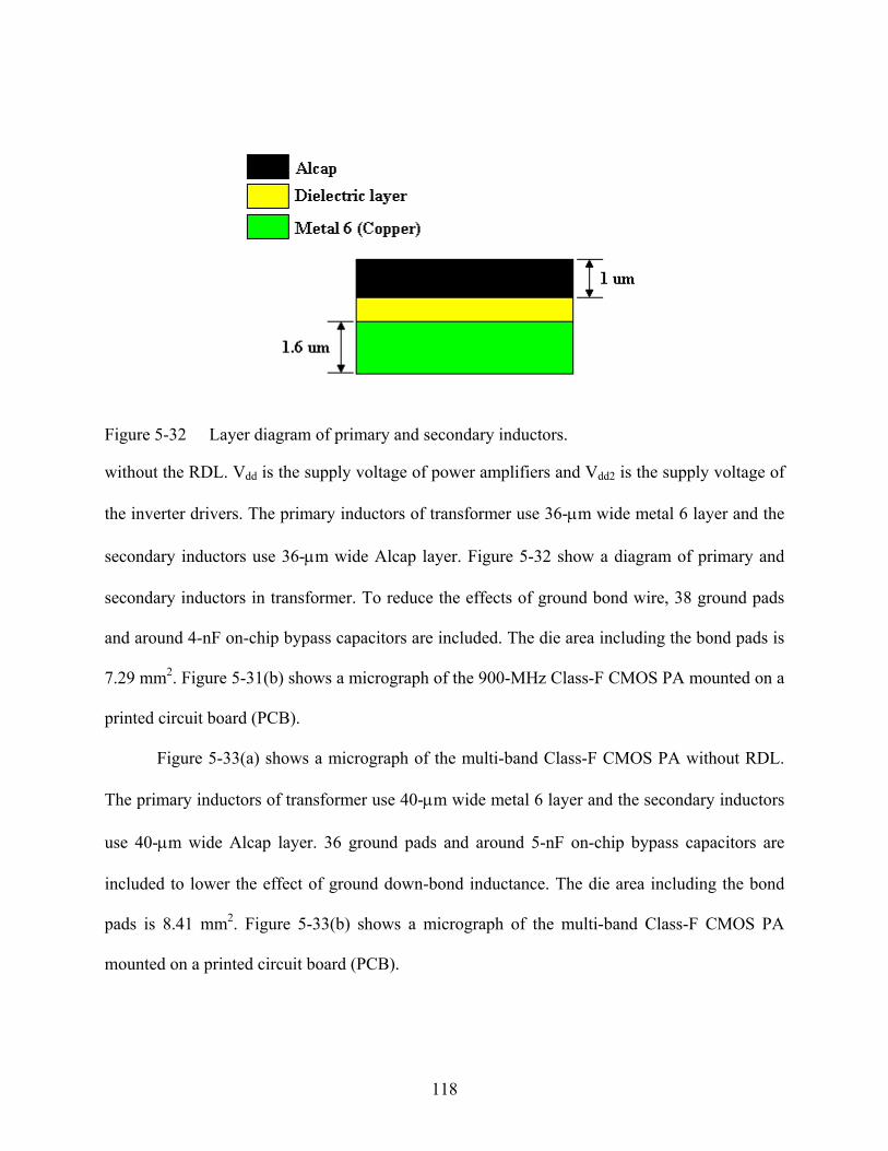
118
Figure 5-32 Layer diagram of primary and secondary inductors.
without the RDL. Vdd is the supply voltage of power amplifiers and Vdd2 is the supply voltage of
the inverter drivers. The primary inductors of transformer use 36-μm wide metal 6 layer and the
secondary inductors use 36-μm wide Alcap layer. Figure 5-32 show a diagram of primary and
secondary inductors in transformer. To reduce the effects of ground bond wire, 38 ground pads
and around 4-nF on-chip bypass capacitors are included. The die area including the bond pads is
7.29 mm2. Figure 5-31(b) shows a micrograph of the 900-MHz Class-F CMOS PA mounted on a
printed circuit board (PCB).
Figure 5-33(a) shows a micrograph of the multi-band Class-F CMOS PA without RDL.
The primary inductors of transformer use 40-μm wide metal 6 layer and the secondary inductors
use 40-μm wide Alcap layer. 36 ground pads and around 5-nF on-chip bypass capacitors are
included to lower the effect of ground down-bond inductance. The die area including the bond
pads is 8.41 mm2. Figure 5-33(b) shows a micrograph of the multi-band Class-F CMOS PA
mounted on a printed circuit board (PCB).
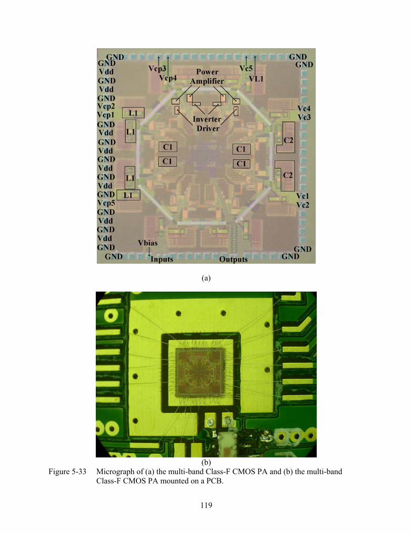
119
(a)
(b)
Figure 5-33 Micrograph of (a) the multi-band Class-F CMOS PA and (b) the multi-band Class-F CMOS PA mounted on a PCB.
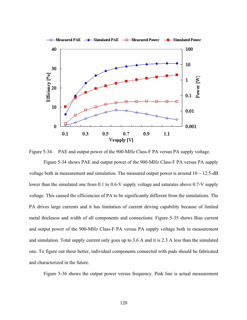
120
Figure 5-34 PAE and output power of the 900-MHz Class-F PA versus PA supply voltage.
Figure 5-34 shows PAE and output power of the 900-MHz Class-F PA versus PA supply
voltage both in measurement and simulation. The measured output power is around 10 ~ 12.5-dB
lower than the simulated one from 0.1 to 0.6-V supply voltage and saturates above 0.7-V supply
voltage. This caused the efficiencies of PA to be significantly different from the simulations. The
PA drives large currents and it has limitation of current driving capability because of limited
metal thickness and width of all components and connections. Figure 5-35 shows Bias current
and output power of the 900-MHz Class-F PA versus PA supply voltage both in measurement
and simulation. Total supply current only goes up to 3.6 A and it is 2.3 A less than the simulated
one. To figure out these better, individual components connected with pads should be fabricated
and characterized in the future.
Figure 5-36 shows the output power versus frequency. Pink line is actual measurement
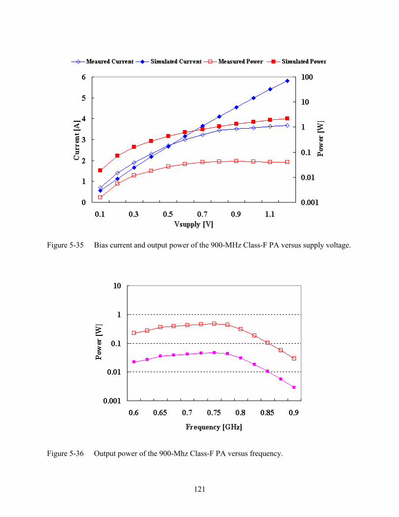
121
Figure 5-35 Bias current and output power of the 900-MHz Class-F PA versus supply voltage.
Figure 5-36 Output power of the 900-Mhz Class-F PA versus frequency.
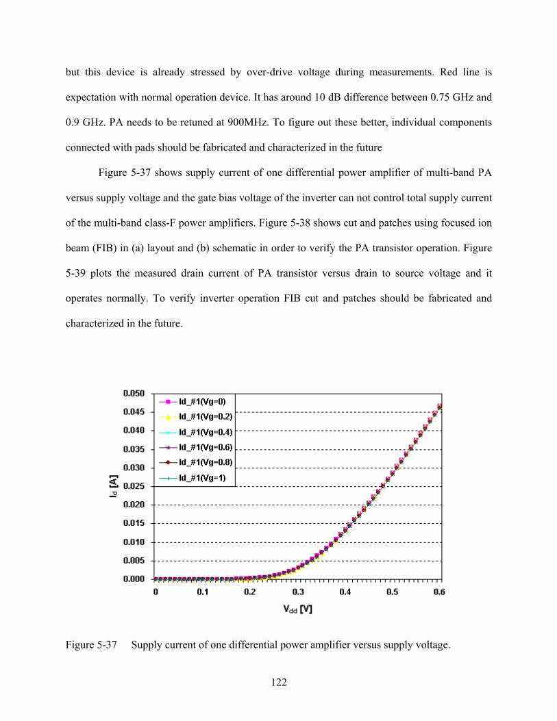
122
but this device is already stressed by over-drive voltage during measurements. Red line is
expectation with normal operation device. It has around 10 dB difference between 0.75 GHz and
0.9 GHz. PA needs to be retuned at 900MHz. To figure out these better, individual components
connected with pads should be fabricated and characterized in the future
Figure 5-37 shows supply current of one differential power amplifier of multi-band PA
versus supply voltage and the gate bias voltage of the inverter can not control total supply current
of the multi-band class-F power amplifiers. Figure 5-38 shows cut and patches using focused ion
beam (FIB) in (a) layout and (b) schematic in order to verify the PA transistor operation. Figure
5-39 plots the measured drain current of PA transistor versus drain to source voltage and it
operates normally. To verify inverter operation FIB cut and patches should be fabricated and
characterized in the future.
Figure 5-37 Supply current of one differential power amplifier versus supply voltage.
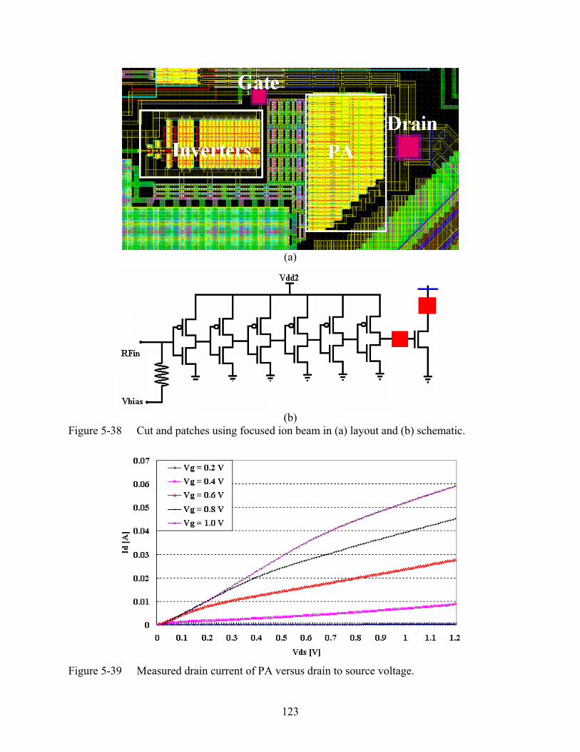
123
(a)
(b)
Figure 5-38 Cut and patches using focused ion beam in (a) layout and (b) schematic.
Figure 5-39 Measured drain current of PA versus drain to source voltage.
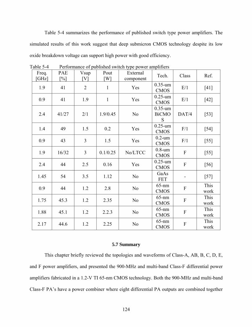
124
Table 5-4 summarizes the performance of published switch type power amplifiers. The
simulated results of this work suggest that deep submicron CMOS technology despite its low
oxide breakdown voltage can support high power with good efficiency.
Table 5-4 Performance of published switch type power amplifiers Freq. [GHz]
PAE [%]
Vsup [V]
Pout [W]
External component Tech. Class Ref.
1.9 41 2 1 Yes 0.35-um CMOS E/1 [41]
0.9 41 1.9 1 Yes 0.25-um CMOS E/1 [42]
2.4 41/27 2/1 1.9/0.45 No 0.35-um BiCMO
S DAT/4 [53]
1.4 49 1.5 0.2 Yes 0.25-um CMOS F/1 [54]
0.9 43 3 1.5 Yes 0.2-um CMOS F/1 [55]
1.9 16/32 3 0.1/0.25 No/LTCC 0.8-um CMOS F [55]
2.4 44 2.5 0.16 Yes 0.25-um CMOS F [56]
1.45 54 3.5 1.12 No GaAs FET - [57]
0.9 44 1.2 2.8 No 65-nm CMOS F This
work
1.75 45.3 1.2 2.35 No 65-nm CMOS F This
work
1.88 45.1 1.2 2.2.3 No 65-nm CMOS F This
work
2.17 44.6 1.2 2.25 No 65-nm CMOS F This
work
5.7 Summary
This chapter briefly reviewed the topologies and waveforms of Class-A, AB, B, C, D, E,
and F power amplifiers, and presented the 900-MHz and multi-band Class-F differential power
amplifiers fabricated in a 1.2-V TI 65-nm CMOS technology. Both the 900-MHz and multi-band
Class-F PA’s have a power combiner where eight differential PA outputs are combined together
125
in order to achieve sufficient output power. The multi-band PA has tunable harmonic peaking
network which consists of variable capacitance and inductance and it also has variable matching
capacitors in both the primary and secondary inductors. In simulation, the maximum efficiency
of 40.6 % and output power of 2.76 W can be achieved from the 900-MHz Class-F power
amplifier. The multi-band Class-F PA can support in EGSM 900, DCS 1800, PCS 1900, and
WCDMA operation. It has simulated PAE of 44 % and output power of 2.8 W at 900 MHz, and
simulated PAE’s of 44.6 ~ 45.3 % and output powers of 2.25 ~ 2.35 W in the high frequency
bands.
The multi-band Class-F CMOS power amplifier can provide the convenience of
designing a multi-band transmitter and save cost and power by realizing a multi-band polar
transmitter. The results of this work suggest that a multi-band power amplifier using deep sub-
micron CMOS technology is possible.
126
CHAPTER 6 SUMMARY AND FUTURE WORK
6.1 Summary
A multi-band radio frequency (RF) transceiver which consists of direct conversion
receiver and polar transmitter that can support EGSM 900, DCS 1800, PCS 1900, and WCDMA
operations is proposed. The feasibility study of possible transmitter and receiver architectures
has been carried out. In the proposed multi-band transceiver, multi-band polar transmitter can
reduce power consumption by a using a high efficiency multi-band power amplifier and lower
cost and area by increasing hardware sharing. The proposed receiver can also lower power
consumption, area and cost by once again increasing hardware sharing using a multi-band LNA
with an SP4T RF switch, wide band mixer variable gain amplifier and tunable low pass filters.
A single-pole-four-throw RF CMOS switch to select one signal among the EGSM 900,
DCS 1800, PCS 1900, and WCDMA from off-chip SAW filters & duplexer to a multi-band
LNA is fabricated and its performance is presented. Since the noise figures of front-end passive
components are directly added to the noise figure of receiver, the design of SP4T switch focused
on lowering insertion losses. The SP4T switch which consists of four transistors and four gate
resistors is designed in a simple topology to minimize the insertion loss. The shunt transistors in
typically formed SPDT CMOS switches have been removed because it increases the insertion
loss. The switch achieves the maximum insertion loss of less than 0.5 dB for four standard
frequency bands, which is acceptable for the multi-band LNA applications. It also has reasonable
isolation and linearity and should be sufficient for the proposed multi-band receiver.
A multi-band LNA with an SP4T RF switch is demonstrated in a UMC 90-nm
technology. The multi-band LNA has variable dual input and output matching networks and it
can support EGSM 900, DCS 1800, PCS 1900 and WCDMA operations. It has power gains of
127
19.9, 9.1, 11.5, and 10.1 dB with 9.4-mW power consumption in the EGSM 900, DCS 1800,
PCS 1900, and WCDMA frequency bands, respectively. The noise figures are 1.7, 2.5, 2.5, and
2.6 dB in EGSM 900, DCS 1800, PCS 1900, and WCDMA bands, respectively. The input third-
order intercept points (IIP3) are 2.7, 3.2, 3, and 3.3 dBm at 930, 1805, 1980, and 2110 MHz. A
multi-band & multi-standard receiver needs a multi-band or wideband LNA with low noise and
moderate gain, and the multi-band LNA with an SP4T switch is a good candidate for this
applications.
The 900-MHz and multi-band Class-F differential power amplifiers fabricated in a 1.2-V
TI 65-nm CMOS technology are presented. The multi-band Class-F PA includes power combing
circuits to realize sufficient output power using low break down nano-scale NMOS transistors.
Variable capacitors and inductors are used to implement a variable harmonic peaking network
and it enables the multi-band Class-F PA to support operation in the EGSM 900, DCS 1800, PCS
1900, and WCDMA bands. The variable matching capacitors are implemented using both on-
chip and off-chip components. At 1.2-V supply voltage, the 900-MHz Class-F power amplifier
has the simulated maximum power added efficiency of 40.6 % and simulated output power of
2.76 W. The multi-band Class-F PA working in the EGSM 900, DCS 1800, PCS 1900, and
WCDMA bands has simulated output power of 2.8 W with simulated PAE of 44 % at 900-MHz
EGSM bands and simulated output powers of 2.25~2.35 W with simulated PAE’s of 44.6 ~
45.3 % in the DCS 1800, PCS 1900, and WCDMA frequency bands. The multi-band Class-F
CMOS power amplifier can provide a good platform for a multi-band transmitter to lower cost
and power.
128
6.2 Future Work
6.2.1 Integrated of the CMOS Multi-Band Receiver
The proposed multi-band direct conversion receiver is a possible solution for a multi-
band receiver for the EGSM 900, DCS 1800, PCS 1900, and WCDMA applications. A fully
integrated multi-band receiver in addition to a multi-band LNA with a SP4T RF switch needs
mixers, VGA’s, VCO and tunable low pass filters. Wide band mixers and VCO, and tunable
channel selection filters with design challenges such as wide band tuning range and linearity
should be researched and developed. The multi-band direct conversion receiver needs lots of
tuning components and a digital control system, as well as circuits to generate the control signals
with appropriate level. These circuit should also be integrated into the multi-band radio .
6.2.1 Improvement of 900-MHz and Multi-Band Class-F CMOS Power Amplifiers
The 900-MHz and multi-band Class-F CMOS PA’s are designed using a TI 65-nm
CMOS. However, there are several concerns which need further research. First, they have
leakage currents from main supply to ground. Second, the current driving of PA is significantly
smaller than simulations. Individual components connected with pads should be fabricated and
characterized to understand these two problems better. These results from these should be
incorporated into a new PA design to experimentally demonstrate the tunable PA.
129
APPENDIX EXPERIMENTAL PLOTS OF THE MULTI-BAND LNA WITH THE SP4T RF SWITCH
A.1 Input Matching Plots of the Multi-Band LNA with the SP4T RF Switch
The plots of measured input matching (|S11|) with different controlled voltages listed in
Tables 4-4 and 4-5 are shown in from Figure A-1 to FigureA-6.
A.2 Output Matching Plots of the Multi-Band LNA with the SP4T RF Switch
The plots of measured output matching (|S22|) with different controlled voltages listed in
Tables 4-6, 4-7, and 4-8 are shown in from Figure A-7 to FigureA-15.
A.3 Power Gain Plots of the Multi-Band LNA with the SP4T RF Switch
The plots of measured power gain (|S21|) with different controlled voltages are shown in in
from Figure A-16 to Figure A-21.
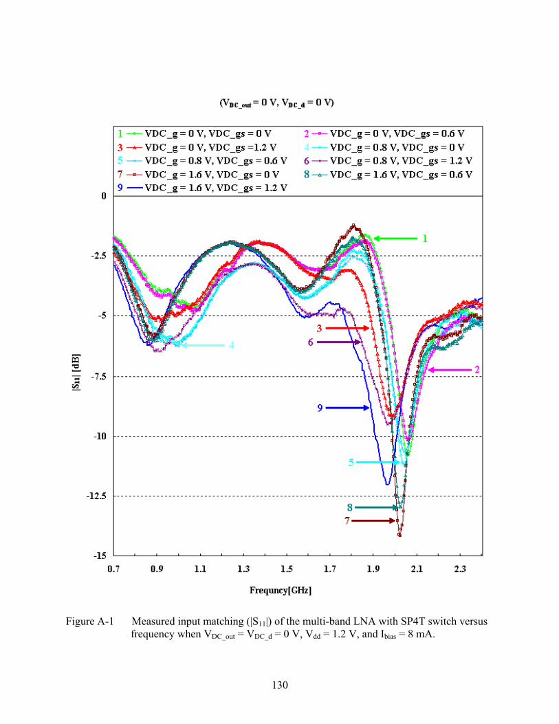
130
Figure A-1 Measured input matching (|S11|) of the multi-band LNA with SP4T switch versus frequency when VDC_out = VDC_d = 0 V, Vdd = 1.2 V, and Ibias = 8 mA.
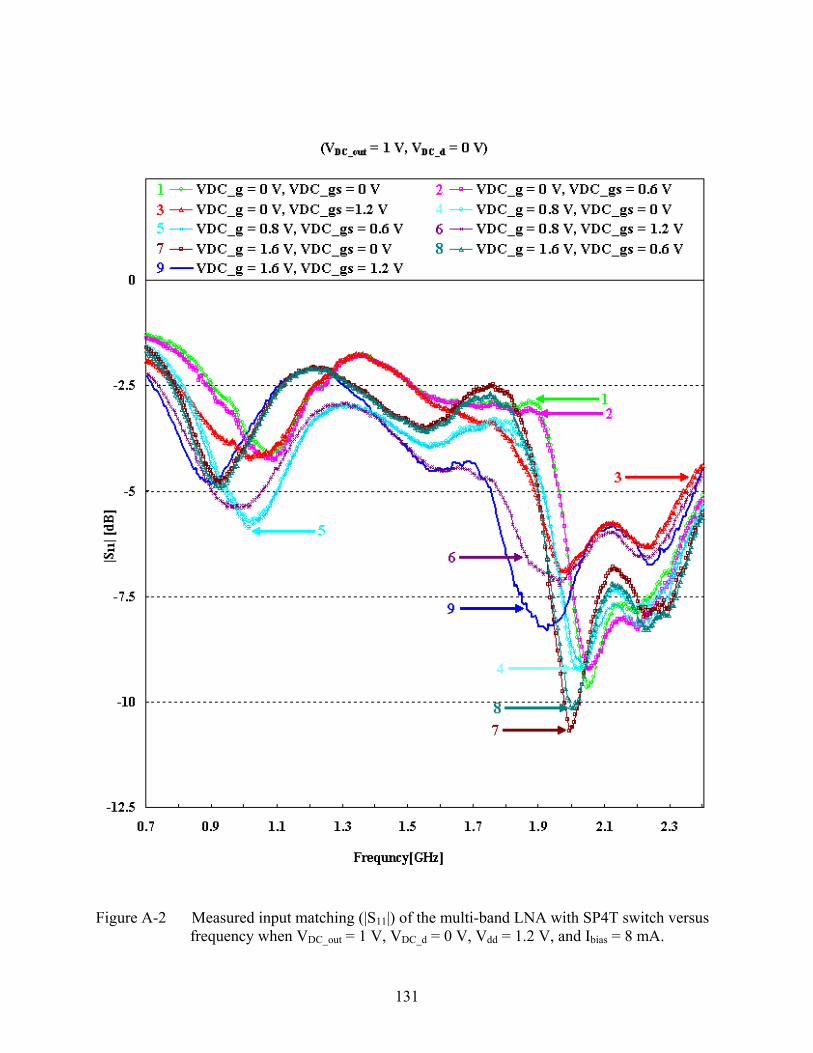
131
Figure A-2 Measured input matching (|S11|) of the multi-band LNA with SP4T switch versus
frequency when VDC_out = 1 V, VDC_d = 0 V, Vdd = 1.2 V, and Ibias = 8 mA.
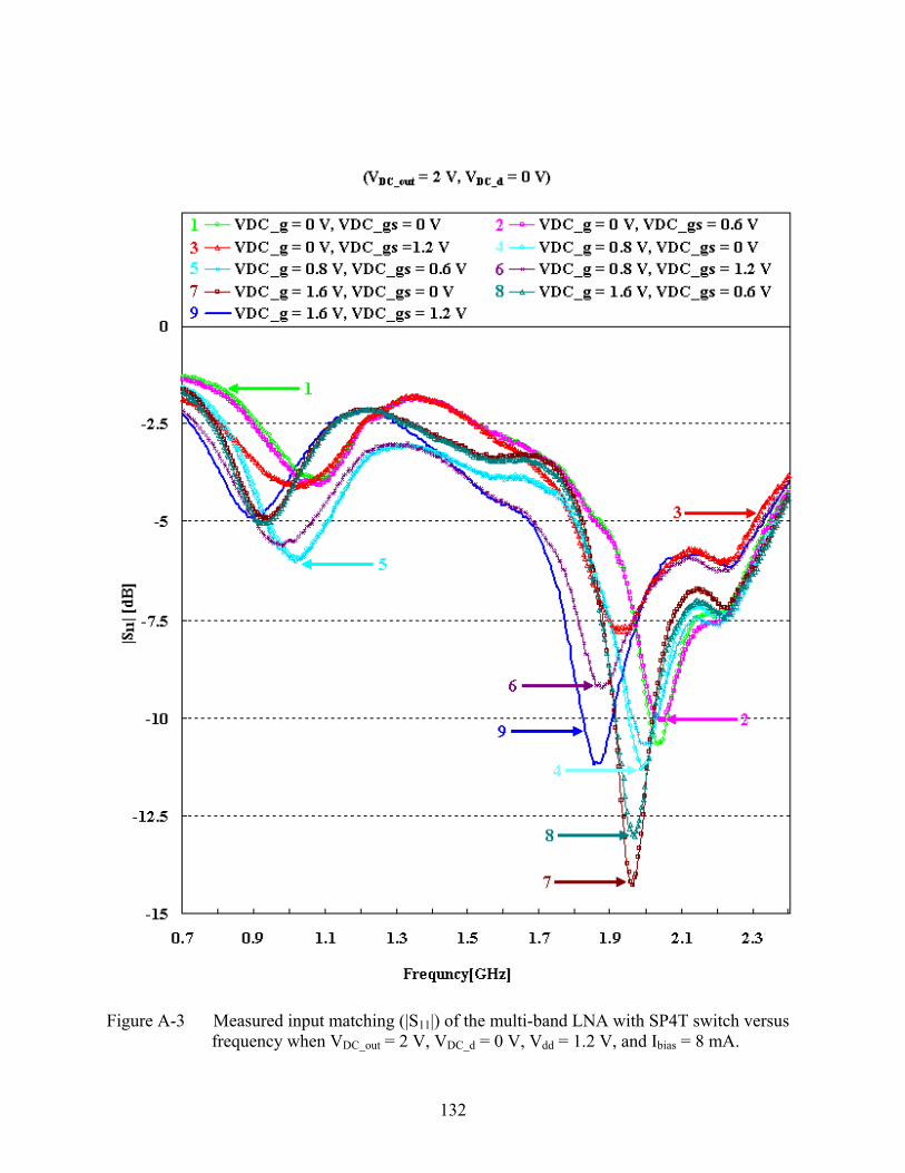
132
Figure A-3 Measured input matching (|S11|) of the multi-band LNA with SP4T switch versus frequency when VDC_out = 2 V, VDC_d = 0 V, Vdd = 1.2 V, and Ibias = 8 mA.
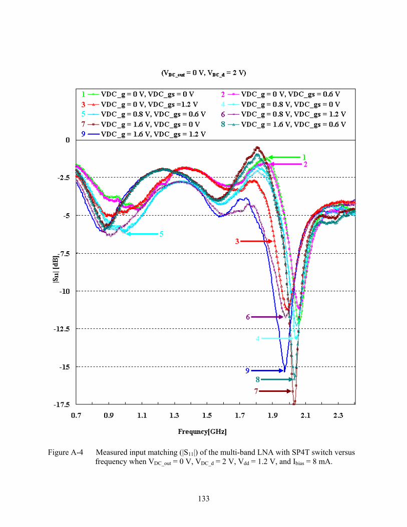
133
Figure A-4 Measured input matching (|S11|) of the multi-band LNA with SP4T switch versus frequency when VDC_out = 0 V, VDC_d = 2 V, Vdd = 1.2 V, and Ibias = 8 mA.
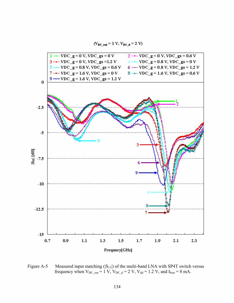
134
Figure A-5 Measured input matching (|S11|) of the multi-band LNA with SP4T switch versus
frequency when VDC_out = 1 V, VDC_d = 2 V, Vdd = 1.2 V, and Ibias = 8 mA.
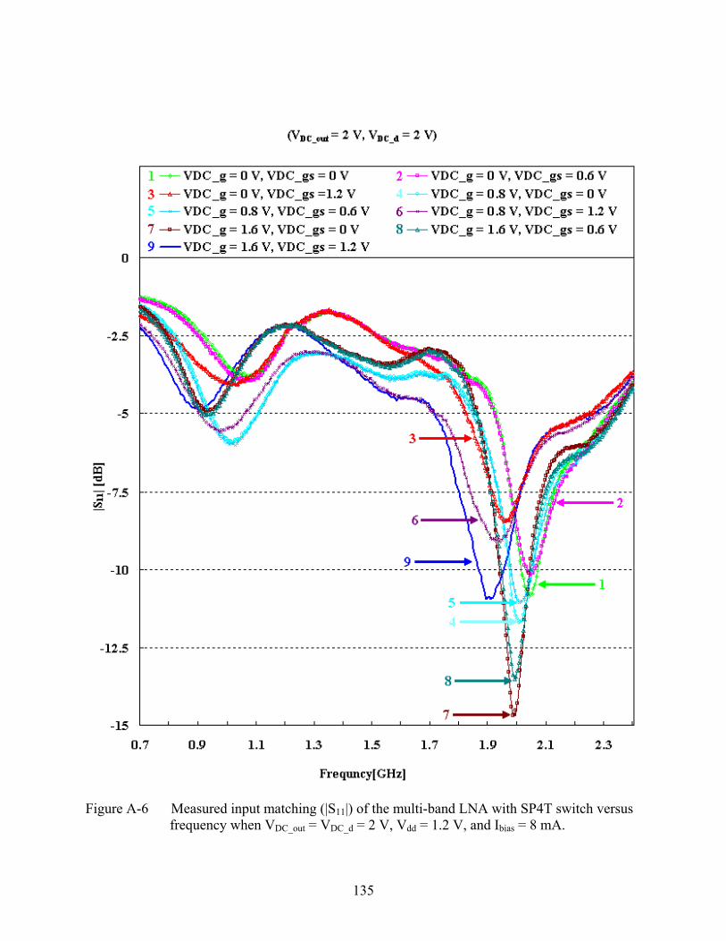
135
Figure A-6 Measured input matching (|S11|) of the multi-band LNA with SP4T switch versus frequency when VDC_out = VDC_d = 2 V, Vdd = 1.2 V, and Ibias = 8 mA.
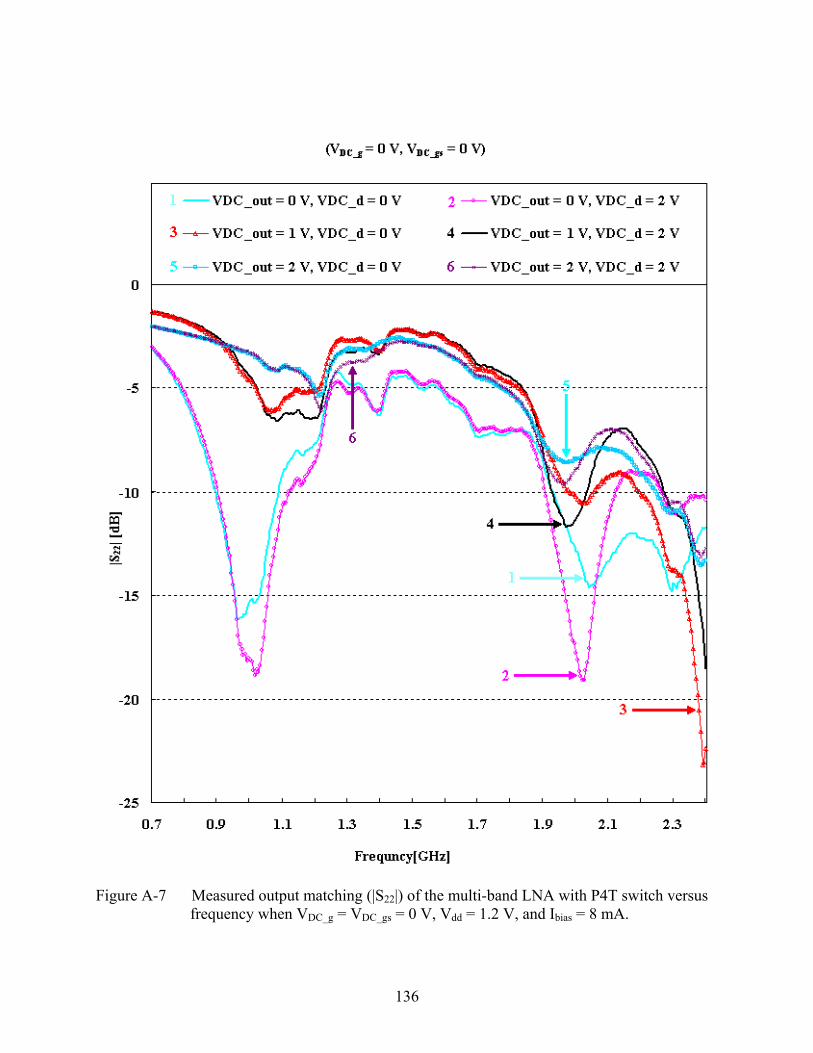
136
Figure A-7 Measured output matching (|S22|) of the multi-band LNA with P4T switch versus frequency when VDC_g = VDC_gs = 0 V, Vdd = 1.2 V, and Ibias = 8 mA.
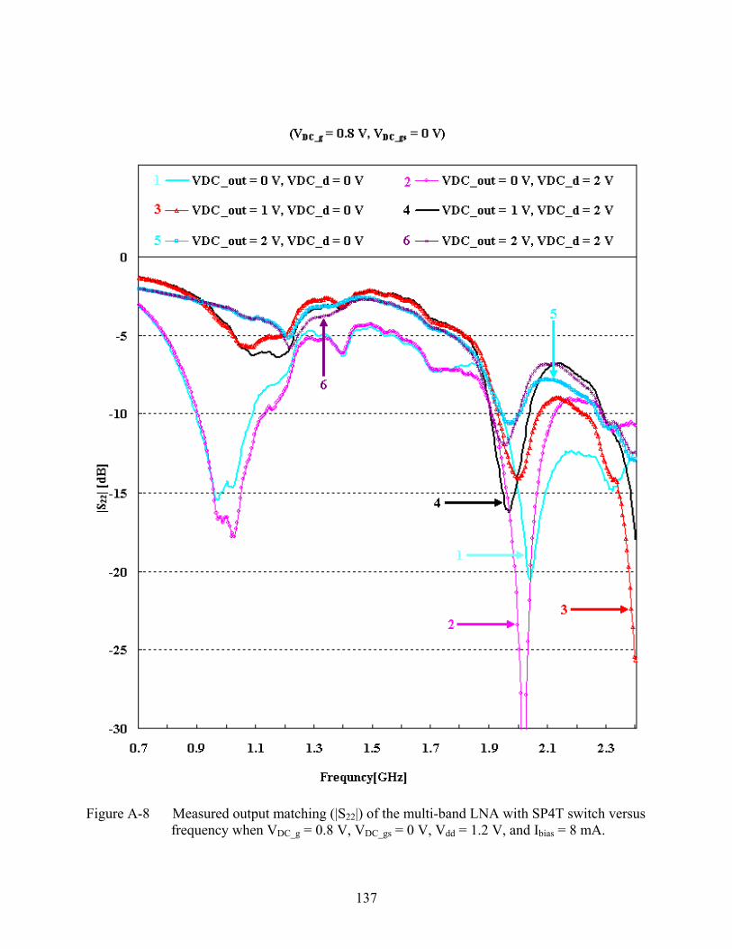
137
Figure A-8 Measured output matching (|S22|) of the multi-band LNA with SP4T switch versus frequency when VDC_g = 0.8 V, VDC_gs = 0 V, Vdd = 1.2 V, and Ibias = 8 mA.
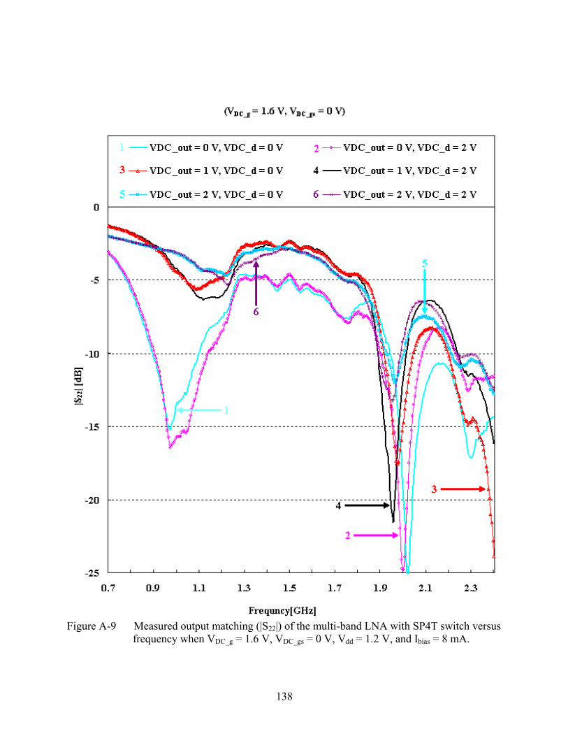
138
Figure A-9 Measured output matching (|S22|) of the multi-band LNA with SP4T switch versus
frequency when VDC_g = 1.6 V, VDC_gs = 0 V, Vdd = 1.2 V, and Ibias = 8 mA.
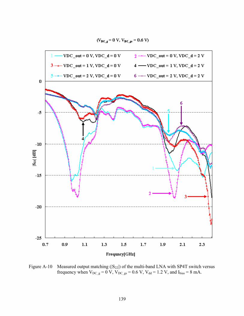
139
Figure A-10 Measured output matching (|S22|) of the multi-band LNA with SP4T switch versus frequency when VDC_g = 0 V, VDC_gs = 0.6 V, Vdd = 1.2 V, and Ibias = 8 mA.
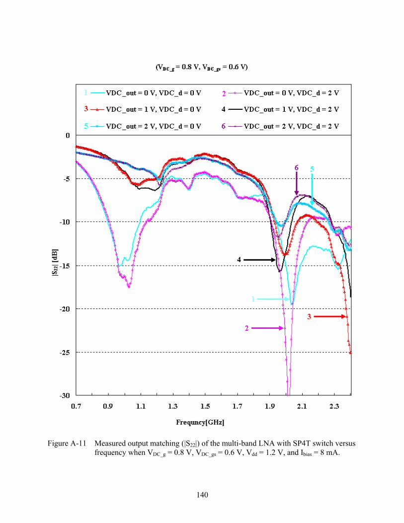
140
Figure A-11 Measured output matching (|S22|) of the multi-band LNA with SP4T switch versus frequency when VDC_g = 0.8 V, VDC_gs = 0.6 V, Vdd = 1.2 V, and Ibias = 8 mA.
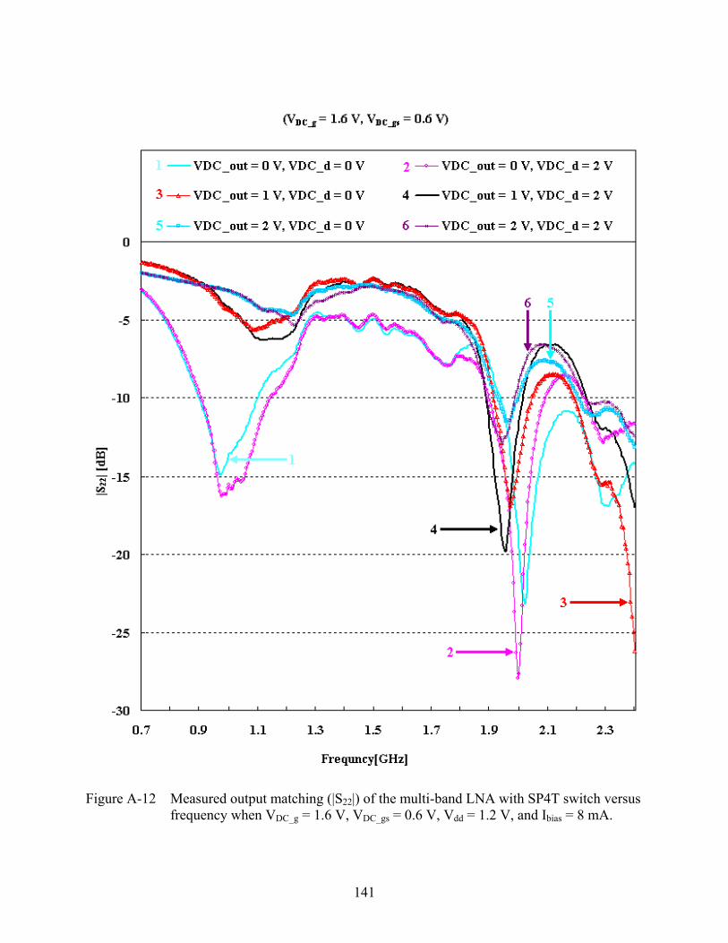
141
Figure A-12 Measured output matching (|S22|) of the multi-band LNA with SP4T switch versus frequency when VDC_g = 1.6 V, VDC_gs = 0.6 V, Vdd = 1.2 V, and Ibias = 8 mA.
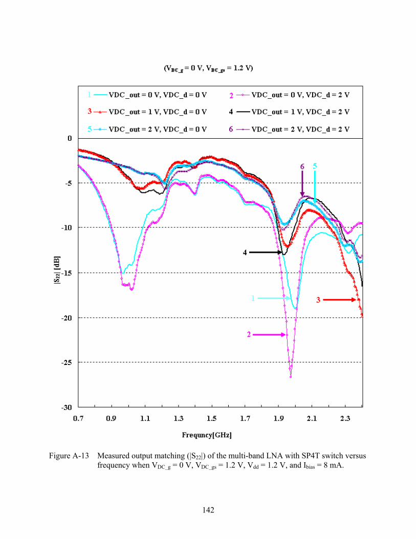
142
Figure A-13 Measured output matching (|S22|) of the multi-band LNA with SP4T switch versus frequency when VDC_g = 0 V, VDC_gs = 1.2 V, Vdd = 1.2 V, and Ibias = 8 mA.
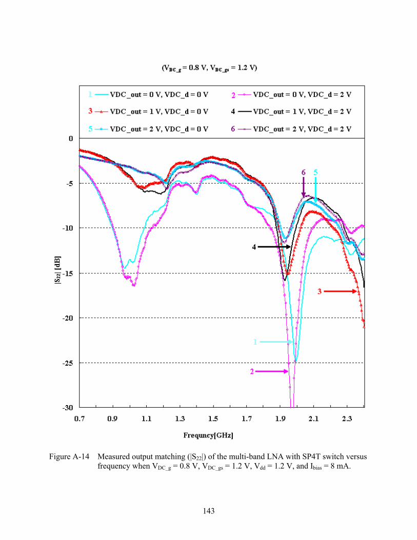
143
Figure A-14 Measured output matching (|S22|) of the multi-band LNA with SP4T switch versus frequency when VDC_g = 0.8 V, VDC_gs = 1.2 V, Vdd = 1.2 V, and Ibias = 8 mA.
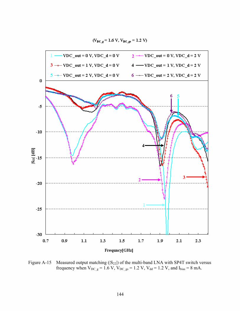
144
Figure A-15 Measured output matching (|S22|) of the multi-band LNA with SP4T switch versus frequency when VDC_g = 1.6 V, VDC_gs = 1.2 V, Vdd = 1.2 V, and Ibias = 8 mA.
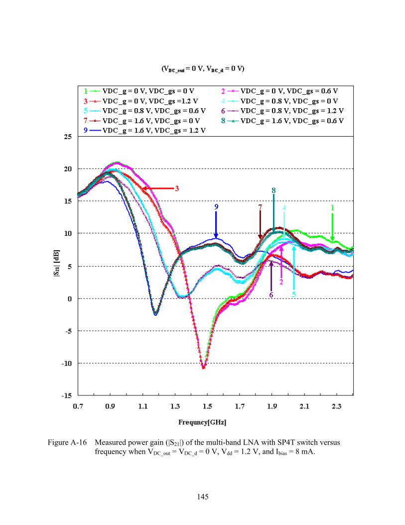
145
Figure A-16 Measured power gain (|S21|) of the multi-band LNA with SP4T switch versus frequency when VDC_out = VDC_d = 0 V, Vdd = 1.2 V, and Ibias = 8 mA.
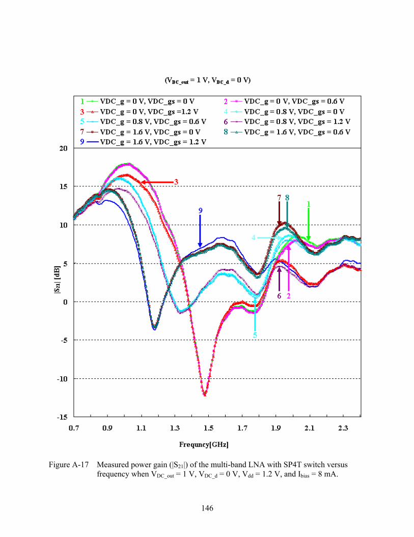
146
Figure A-17 Measured power gain (|S21|) of the multi-band LNA with SP4T switch versus frequency when VDC_out = 1 V, VDC_d = 0 V, Vdd = 1.2 V, and Ibias = 8 mA.
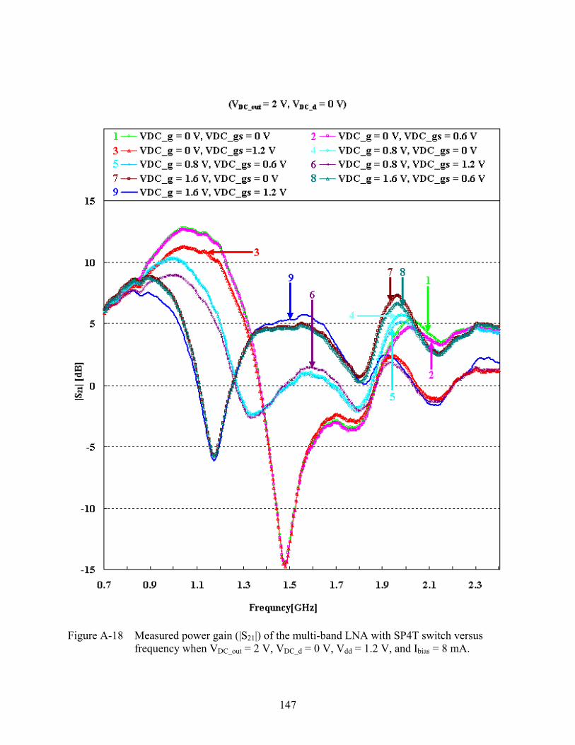
147
Figure A-18 Measured power gain (|S21|) of the multi-band LNA with SP4T switch versus frequency when VDC_out = 2 V, VDC_d = 0 V, Vdd = 1.2 V, and Ibias = 8 mA.
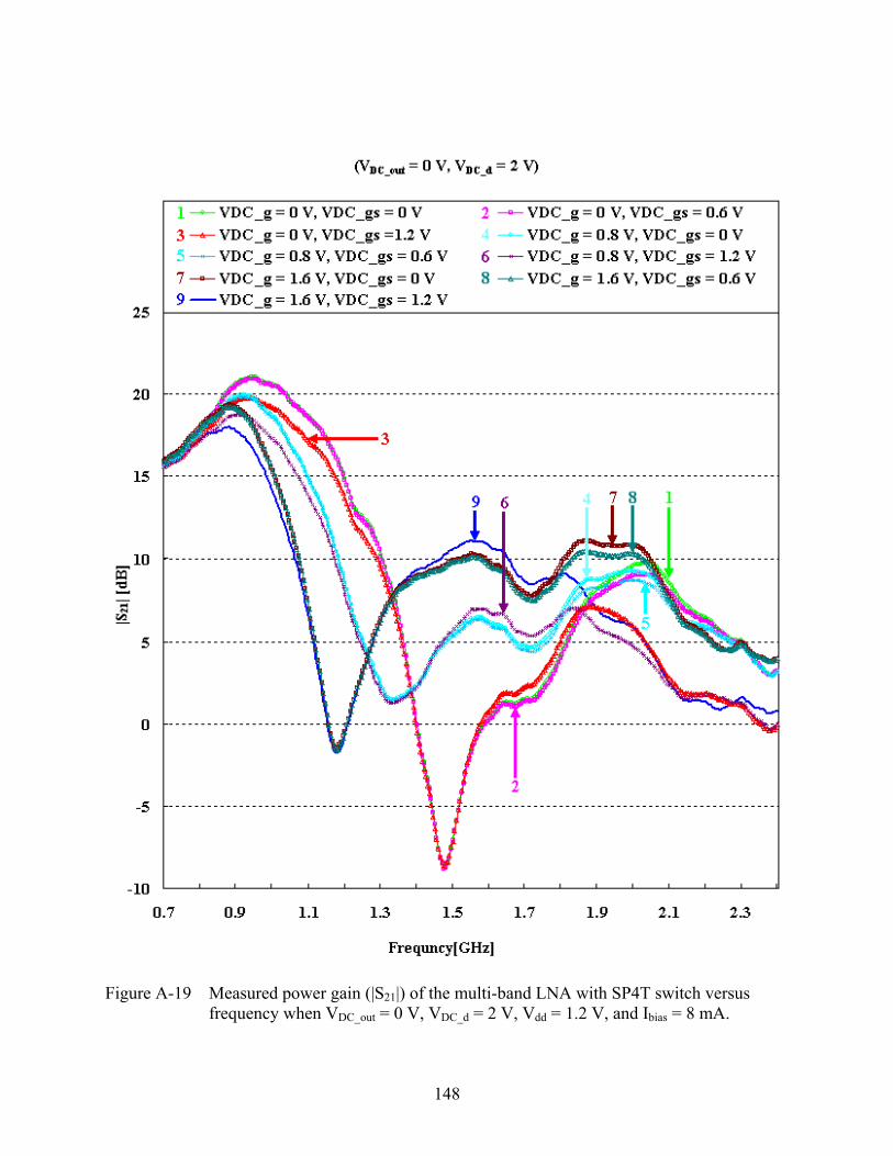
148
Figure A-19 Measured power gain (|S21|) of the multi-band LNA with SP4T switch versus frequency when VDC_out = 0 V, VDC_d = 2 V, Vdd = 1.2 V, and Ibias = 8 mA.
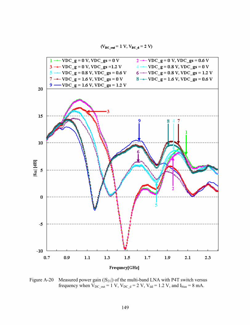
149
Figure A-20 Measured power gain (|S21|) of the multi-band LNA with P4T switch versus frequency when VDC_out = 1 V, VDC_d = 2 V, Vdd = 1.2 V, and Ibias = 8 mA.
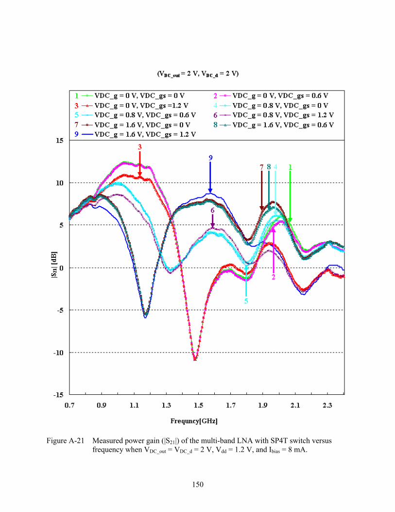
150
Figure A-21 Measured power gain (|S21|) of the multi-band LNA with SP4T switch versus frequency when VDC_out = VDC_d = 2 V, Vdd = 1.2 V, and Ibias = 8 mA.
151
LIST OF REFERENCES
[1] L. Maurer, K.Chabrak, and R. Weigel, “Design of mobile radio transceiver RFICs: Current status and future trends,” in Int. Control, Communications and Signal Processing Symp., 2004, pp. 53-56.
[2] R. Magoon, A. Molnar, J. Zachan, G. Hatcher, and W. Rhee, “A single-chip quad-band (850/900/1800/1900 MHz) direct conversion GSM/SPRS RF transceiver with integrated VCOs and fractional-N synthesizer,” IEEE J. of Solid-State Circuits, vol. 37, no. 12, pp. 1710-1720, Dec. 2002.
[3] J. Ryynänen, K. Kivekäs, J. Jussila, L. Sumanen, A. Pärssinen, and K. A. I. Halonen, “A single-chip multimode receiver for GSM900, DCS1800, PCS1900, and WCDMA,” IEEE J. of Solid-State Circuits, vol. 38, no. 4, pp. 594-602, Apr. 2003.
[4] E. Gotz, H. Krobel, G. Marzinger, B. Memmler, C. Munker, B. Neurauter, D. Romer, J. Rubach, W. Schelmbauer, M. Scholz, M. Simon, U. Steinacker, and C. Stoger, “A quad-band low power single chip direct conversion CMOS transceiver with /spl Sigma//spl Delta/-modulation loop for GSM,” in Proc. Eur. Solid-State Circuits Conf., Sep. 2003, pp. 217-220.
[5] E. Duvivier, S. Cipriani, L. Carpineto, P. Cusinato, B. Bisanti, F. Galant, F. Chalet, F. Coppola, S. Cercelaru, G. Puccio, N. Mouralis, and J.C. Jiguet, “A fully integrated zero-IF transceiver for GSM-GPRS quad band application,” IEEE J. of Solid-State Circuits, vol. 38, no. 12, pp. 2249-2257, Dec. 2003.
[6] S. M. Yim, “Components and circuit techniques for a multi-band wireless receiver,” Ph.D. dissertation, University of Florida, FL, Dec. 2003.
[7] K. Jung and K. O, “A CMOS single-pole-four-throw switch,” IEEE Microw. Wireless Component Lett., vol. 16, no.3, pp. 128-130, Mar. 2006.
[8] Digital Cellular Telecommunications System (Phase 2); Radio Transmission and Reception, GSM standard 05 05, 1999.
[9] J. E. Brittain, The Legacies of Edwin Howard Armstrong. Littleton, CO: The Radio Club of America, 1991.
[10] B. Razavi, RF Microelctronics. Upper Saddle River, NJ: Prentice Hall, 1998.
[11] R. C. Sagers, “Intercept point and undesired responses,” IEEE Trans. Vehicular Tech., vol. 32, no. 1, pp. 121-133, Feb. 1983.
[12] M. R. Elliott, T. Montalvo, B. P. Jeffries, F. Murden, J. Strange, A. Hill, S. Nandipaku, and J. Harrebek “A polar modulator transmitter for GSM/EDGE,” IEEE J. of Solid-State Circuits, vol. 39, no. 12, pp. 2190-2199, Dec. 2004.
152
[13] M. Brandolini, P. Rossi, D. Manstretta, and F. Svelto, “Toward multistandard mobile terminals-fully integrated receiver requirements and architectures,” IEEE Trans. Microw. Theory and Tech., vol. 53, no. 3, pp. 1026-1038, Mar. 2005.
[14] “UAA3535HL-Low power GSM/DCS/PCS multi-band transceiver,” Philips Semiconductor, Sunnyvale, CA, Data Sheet, Feb. 17, 2000. [Online]. Available: www.semiconductors.phi- lips.com
[15] “DFYK61G95LBJCA,” Murata, Kyoto, Japan. 2006. [Online]. Available: www.murata.com
[16] F. J. Huang and K. O, “A 0.5-μm CMOS T/R switches for 900-MHz wireless applications,” IEEE J. of Solid-State Circuits, vol. 36, no. 3, pp. 486-492, Mar. 2001.
[17] Z. Li, H. Yoon, F.J. Huang and K. O, “5.8-GHz CMOS T/R switches with high and low substrate resistances in a 0.18-μm CMOS process,” IEEE Microw. Wireless Component Lett., vol. 13, no.1, pp. 1-3, Jan. 2003.
[18] “ASW5524/ASW5532R SP4T/SPDT switches,” Anadigics, Inc., [Online]. Available: www.anadigics.com
[19] T. Ohnakado, S. Yamkawa, T. Murakami, A. Furukawa, E. Taniguchi, H. Ueda, N. Suematsu, and T. Oomori, “21.5-dBm power-handling 5-GHz transmit/receive CMOS switch realized by voltage division effect of stacked transistor configuration with depletion-layer-extended transistors (DETs),” IEEE J. of Solid-State Circuits, vol. 39, no. 4, pp. 577-695, Apr. 2004.
[20] N. A. Talwalkar, C. P. Yue, H. Gan and S. S Wong, “Integrated CMOS transmit-receive switch using LC-tuned substrate bias for 2.4-GHz and 5.2-GHz applications,” IEEE J. of Solid-State Circuits, vol. 39, no. 6, pp. 863-870, Jun. 2004
[21] A. Springer and R. Weiger, “RF system concepts for highly integrated RFICs for W-CDMA mobile radio terminals,” IEEE Trans. Microw. Theory and Tech., vol. 50, no. 1, pp. 254-267, Jan. 2002.
[22] H. T. Friis, “Noise Figures of Radio Receivers,” Proc. IRE, vol. 32, no. 7, pp. 419-422, Jul. 1944.
[23] Y.-C. Ho, “Implementation and improvement for RF low noise amplifiers in conventional CMOS technologies,” Ph.D. dissertation, University of Florida, FL, Dec. 2000.
[24] D. K. Shaeffer and T. H. Lee, The Design and Implementation of Low-Power CMOS Radio Receivers. Boston, MA: Kluwer, 1999.
[25] B. A. Floyd, “A CMOS Wireless Interconnect System for Multigigahertz Clock Distribution,” Ph.D. dissertation, University of Florida, FL, May 2001.
[26] A. van der Ziel, Noise in Solid State Devices and Circuits. New York: Wiley, 1986.
153
[27] D. K. Shaeffer and T. H. Lee, “A 1.5-V, 1.5GHz CMOS Low Noise Amplifier,” IEEE J. of Solid-State Circuits, vol. 32, no. 5, pp.745-759, May 1997.
[28] D. K. Shaeffer and T. H. Lee, “ Corrections to “ A 1.5-V, 1.5GHz CMOS Low Noise Amplifier”,” IEEE J. of Solid-State Circuits, vol. 40, no. 6, pp.1397-1398, Jun. 2005.
[29] J.-S. Goo, H.-T. Ahn, D.J. Ladwig, Z. Yu, T.H. Lee, and R.W Dutton, “A Noise Optimization Technique for Integrated Low-Noise Amplifiers,” IEEE J. of Solid-State Circuits, vol. 37, no. 8, pp.994-1002, Aug. 2002.
[30] B. G. Perumana, J. C. Zhan, S. S. Taylor, B. R. Carlton, and J. Laskar, “Resistive-feedback CMOS low-noise amplifier for multiband applications,” IEEE Trans. Microw. Theory and Tech., vol. 56, no. 5, pp. 1118-1225, May 2008.
[31] H. Hashemi and A. Hajimiri, “Concurrent dual-band CMOS low noise amplifiers and receiver architectures,” ” in VLSI Circuits Tech. Sym. Dig, Jun. 2001, pp. 247-250.
[32] C.-M. Hung, Y.-C. Ho, I.-C. Wu, and K. O, “High-Q capacitors implemented in a CMOS process for low-power wireless applications,” IEEE Trans. Microw. Theory and Tech., vol. 46, no. 5, pp. 505–511, May. 1998.
[33] “Noise figure measurement accuracy—The Y factor method,” in Agilent Technologies Application Note 57-2.
[34] S. Andersson, C. Svensson and O Drugge, “Wideband LNA for a multistandard wireless receiver in 0.18 μm CMOS,” in Proc. Eur. Solid-State Circuits Conf. , Sep. 2003, pp. 655-658.
[35] R.-C. Liu, C.-S. Lin, K.-L.Deng, and H. Wang, “A 0.5-14 GHz 10.6-dB CMOS cascade distributed amplifier,” in VLSI Circuits Tech. Sym. Dig, Jun. 2003, pp. 139-140.
[36] H. Doh, Y. Jeong, S. Jung, and Y. Joo, “Wide-band CMOS low-noise amplifier exploiting thermal noise canceling,” IEEE J. of Solid-State Circuits, vol. 39, no. 2, pp. 275-282, Feb. 2004.
[37] A. Bevilacqua and A. Niknejad, “An ultra-wideband CMOS LNA for 3.1 to 10.6 GHz wireless receivers,” ” IEEE J. of Solid-State Circuits, vol. 39, no. 12, pp. 2259-2268, Dec. 2004.
[38] C.-W. Kim, M. S. Kang, P. T. Anh, H. T. Kim, and S. G. Lee, “An ultra wideband CMOS low noise amplifier for 3−5-GHz UWB systems,” IEEE J. of Solid-State Circuits, vol. 40, no. 2, pp. 544-547, Feb. 2005.
[39] S. Vishwakarma, A. Mirzaei, R. Bagheri, and A. Abidi, “A 6.5 GHz wideband CMOS low noise amplifier for multi-band use,” in Proc. Custom Integrated Circuits Conf., sep. 2005, pp. 801-804.
154
[40] H. Song, H. Kim, K. Han, J. Choi, C Park, and Bumman Kim, “A sub-2 dB NF dual CMOS LNA for CDMA/WCDMA applications,” IEEE Microw. Wireless Component Lett., vol. 18, no.3, pp. 212-214, Mar. 2008.
[41] K. C. Tsai and P. R. Gray, “A 1.9 GHz, 1-W CMOS Class-E power amplifier for wireless communications,” IEEE J. of Solid-State Circuits, vol. 34, no. 7, pp. 962-969, Jul. 1999.
[42] C. Yoo and Q. Haung, “A common-gate switched 0.9-W Class-E power amplifier with 41% PAE in 0.25-μm CMOS,” IEEE J. of Solid-State Circuits, vol. 36, no. 5, pp. 823-830, May 2001.
[43] H. L. Krauss, C. W. Bostian, and F. H. Raab, Solid State Radio Engineering. New York: Wiley, 1980.
[44] T. H. Lee, The Design of CMOS Radio-Frequency Integrated Circuits. Cambridge U.K., Cambridge University Press, 1998.
[45] N. O. Sokal and A. D. Sokal, “Class E-a new Class of high efficiency tuned single-ended switching power amplifiers,” IEEE J. of Solid-State Circuits, vol. 10, no. 3, pp. 168-176, Jun. 1975.
[46] F. H. Raab, “Introduction to Class-F power amplifiers,” RF Design, vol. 19, no. 5, pp. 79-84, May 1996.
[47] T. Sowlati, D. Rozenblit, E. MacCarthy, M. Damgaard, R. Pullela, D. Koh, and D. Ripley, “Quad Band GSM/GPRS/EDGE. Polar Loop Transmitter,” IEEE J. of Solid-State Circuits, vol. 39, no. 12, pp. 2179-2189, Dec. 2004.
[48] G. Liu, T.-J. King, and A. M. Niknejad, “A 1.2V, 2.4 GHz fully integrated linear CMOS power amplifier with efficiency enhancement,” in Proc. Custom Integrated Circuits Conf., Sep. 2006, pp. 141-144.
[49] C. Trask, “Class-F amplifier loading networks: a unified design approach,” ” in IEEE MTT-S Dig., vol1, Jun. 13-19, 1999, pp. 351-354.
[50] A. V. Grebennikov, “Circuit design technique for high efficiency Class F amplifier, ” in IEEE MTT-S Dig., vol. 2, Jun. 11-16, 1999, pp. 771-774.
[51] S. Yim and K. K. O, “Demonstration of a Switched Resonator Concept in a Dual-Band-Monolithic CMOS LC-Tuned VCO,” in Proc. Custom Integrated Circuits Conf. , 2001, pp. 205-208.
[52] S. R. Whiteley. (2001, Feb.). FastHenry Version 3.0wr. [Online]. Available: http://www.sr-ware.com
[53] I. Aoki, S. D. Kee, D. B. Rutledge, and A. Hajimiri, “Fully integrated CMOS power amplifier design using the distributed active-transformer architecture,” IEEE J. of Solid-State Circuits, vol. 37, no.3, pp. 371-383, Mar. 2002.
155
[54] A. Shirvani, D. K. Su, and B. A. Wooley, “A CMOS RF Power Amplifier with Parallel Amplification for Efficient Power Control”, IEEE J. of Solid-State Circuits, vol. 37, no. 6, pp 684-693, Jun. 2002.
[55] T. C. Kuo and B. B. Lusignan, “A 1.5W Class-F RF Power Amplifier in 0.2μm CMOS Technology”, in Int. Solid-State Circuits Conf. Tech. Dig., vol 1, Feb. 2001, pp. 154-155.
[56] Y. J. E. Chen, M. Hamai, D. Heo, A. Sutono, S. Yoo, and J. Laskar, “RF Power Amplifier Integration in CMOS Technology,” in IEEE MTT-S Dig., vol1, May 2000, pp. 545-548.
[57] M. Nishida, S. Murai, H. Uda, H. Tominaga, T. Sawai, and A. Ibaraki, “A high efficiency GaAs power amplifier module with a single voltage for digital cellular phone systems, ” in IEEE MTT-S Dig., vol.2, Jun. 1998, pp. 443 – 446.
156
BIOGRAPHICAL SKETCH
Kwangchun Jung was born in Kimje, South Korea in August 1972. He received the B.E.
and M.S. degrees in electrical engineering from SungKyunKwan University, Suwon in South
Korea in 1995 and 1997, respectively. Since 2007, he has been a Ph.D. candidate in the
department of electrical and computer engineering of the University of Florida, Gainesville and
has been with the Silicon Microwave Integrated Circuits and Systems (SiMICS) research group
since 2003.
After his master’s degree, he worked in Nara Control Inc. in Seoul, South Korea as a
senior engineer. Before his studies in the USA, he worked in Texas A&M University as a
visiting scholar. During the summer of 2005, he interned at Bitwave Semicondutor Coporation
where he was involved in CMOS RF system and circuit design. His current research interests are
in analysis and design of multi-band RF transceiver systems, CMOS RFIC, multi-band low noise
amplifiers, multi-band CMOS power amplifiers, and Gm-C filters.


![Pengolahan Citra - Stmik Jakartaaqwam.staff.jak-stik.ac.id/files/30.-pengolahan-citra[15].pdfJenisnya : CCD(charge coupled device) dan CMOS ( complementary metal-oxide semiconductor)](https://static.fdocuments.net/doc/165x107/5e47ca1e991bb60b6f25174c/pengolahan-citra-stmik-15pdf-jenisnya-ccdcharge-coupled-device-dan-cmos.jpg)


![ScanGate document (Charge Coupled Device), CMOS (Complementary Metal Oxide Semiconductor) , alebo DPS (Digital Pixel System). Historický vývoj kamery bol nasledujúci [22]: 1884](https://static.fdocuments.net/doc/165x107/5bbae9af09d3f241268bddc0/scangate-document-charge-coupled-device-cmos-complementary-metal-oxide-semiconductor.jpg)