cmx644ad - AppleLogic · This allows easy interfacing to a host µController. ... Changes and...
32
CMX644A V22 and Bell 212A Modem 1998 Consumer Microcircuits Limited D/644A/2 December 1998 Advance Information Features Applications • V22/Bell 212A Compatible Modem • Telephone Telemetry Systems • Integrated DTMF Encoder • Remote Utility Meter Reading • Call Progress/Accurate Answer Tone Detection • Security Systems/Cash Terminals • Line Reversal and Ringing Detector • Industrial Control Systems • Low Power Operation (2.7V) • Pay-Phones • Fully Integrated UART Functions • Cable TV Set-Top Boxes 1.1 Brief Description The CMX644A V22 modem is intended for use in any telephone based information and telemetry system with low power requirements. Using V22 signalling, fast call set up times and robust error resistant transmission can be implemented by efficient low power circuits. The circuit can operate at 1200b/s full duplex over 2-or 4- wire circuits. Control of the device is via a simple high speed serial bus and data may be optionally formatted by the on-chip UART. This allows easy interfacing to a host μController. The data transmitted and received by the modem is also transferred over the same high speed serial bus. In addition to V22, support is included to meet the Bell 212A standard. The integrated DTMF encoder can be used as part of the dial out function. All 16 DTMF combinations are available along with a single tone ‘melody’ mode. The answer tone generator/detector and call progress tone detectors included on the CMX644A make the set- up of a telephone call a simple matter for the host μController. In many data collection and telemetry systems low power consumption is important. The CMX644A features a ‘Zero Power’ standby mode. Whilst in standby, the device can still detect a ringing voltage or line voltage reversal. The CMX644A can operate on a supply voltage between 3.0V and 5.5V across the full temperature range of -40°C to +85°C. A low impedance pull down output is provided for a hook relay. The CMX644A is pin compatible with the CMX624 V23/Bell 202 modem also from CML.
Transcript of cmx644ad - AppleLogic · This allows easy interfacing to a host µController. ... Changes and...

CMX644AV22 and Bell 212A
Modem
1998 Consumer Microcircuits Limited
D/644A/2 December 1998 Advance Information
Features Applications
•• V22/Bell 212A Compatible Modem •• Telephone Telemetry Systems
•• Integrated DTMF Encoder •• Remote Utility Meter Reading
•• Call Progress/Accurate Answer Tone Detection •• Security Systems/Cash Terminals
•• Line Reversal and Ringing Detector •• Industrial Control Systems
•• Low Power Operation (2.7V) •• Pay-Phones
•• Fully Integrated UART Functions •• Cable TV Set-Top Boxes
1.1 Brief Description
The CMX644A V22 modem is intended for use in any telephone based information and telemetry system withlow power requirements. Using V22 signalling, fast call set up times and robust error resistant transmissioncan be implemented by efficient low power circuits. The circuit can operate at 1200b/s full duplex over 2-or 4-wire circuits. Control of the device is via a simple high speed serial bus and data may be optionally formattedby the on-chip UART. This allows easy interfacing to a host µController. The data transmitted and receivedby the modem is also transferred over the same high speed serial bus. In addition to V22, support is includedto meet the Bell 212A standard. The integrated DTMF encoder can be used as part of the dial out function.All 16 DTMF combinations are available along with a single tone ‘melody’ mode.
The answer tone generator/detector and call progress tone detectors included on the CMX644A make the set-up of a telephone call a simple matter for the host µController.
In many data collection and telemetry systems low power consumption is important. The CMX644A features a‘Zero Power’ standby mode. Whilst in standby, the device can still detect a ringing voltage or line voltagereversal. The CMX644A can operate on a supply voltage between 3.0V and 5.5V across the full temperaturerange of -40°C to +85°C. A low impedance pull down output is provided for a hook relay. The CMX644A ispin compatible with the CMX624 V23/Bell 202 modem also from CML.
V22 and Bell 212A Modem CMX644A
1998 Consumer Microcircuits Limited 2 D/644A/2
CONTENTSSection Page
1.1 Brief Description.........................................................................................1
1.2 Block Diagram ............................................................................................3
1.3 Signal List ...................................................................................................4
1.4 External Components.................................................................................6
1.5 General Description....................................................................................71.5.1 ‘C-BUS’ Interface ..........................................................................71.5.2 UART...........................................................................................81.5.3 Software Description ...................................................................10
1.6 Application Notes.....................................................................................211.6.1 Line Interface ..............................................................................211.6.2 Ring Detector Interface................................................................231.6.3 Software Protocol for Transmitting PSK Data Bytes.....................241.6.4 Software Protocol for Receiving PSK Data Bytes.........................25
1.7 Performance Specification.......................................................................261.7.1 Electrical Performance ................................................................261.7.2 Packaging ...................................................................................31
Note: This product is in development: Changes and additions will be made to this specification. Itemsmarked TBD or left blank will be included in later issues.

V22 and Bell 212A Modem CMX644A
1998 Consumer Microcircuits Limited 3 D/644A/2
1.2 Block Diagram
Figure 1 Block Diagram

V22 and Bell 212A Modem CMX644A
1998 Consumer Microcircuits Limited 4 D/644A/2
1.3 Signal List
CMX644AD2/D5/P4
Signal Description
Pin No. Name Type
1 XTALN O/P The inverted output of the on-chip oscillator.
2 XTAL/CLOCK I/P The input to the on-chip oscillator, for externalXtal circuit or clock.
3 SERIAL CLOCK I/P The ‘C-BUS’ serial clock input. This clock,produced by the µController, is used for thetransfer timing of commands to and from thedevice.
4 COMMAND DATA I/P The ‘C-BUS’ serial data input from theµController. Data is loaded into this device in 8-bit bytes, MSB (B7) first, and LSB (B0) last,synchronised to the SERIAL CLOCK.
5 REPLY DATA T/S The ‘C-BUS’ serial data output to theµController. The transmission of REPLY DATAbytes is synchronised to the SERIAL CLOCKunder control of the CSN input. This 3-stateoutput is held at high impedance when notsending data to the µController.
6 CSN I/P The ‘C-BUS’ data loading control function: thisinput is provided by the µController. Datatransfer sequences are initiated, completed oraborted by the CSN signal.
7 IRQN O/P This output indicates an interrupt condition to theµController by going to a logic ‘0’. This is a‘wire-ORable’ output, enabling the connection ofup to 8 peripherals to 1 interrupt port on theµController. This pin has a low impedancepulldown to logic ‘0’ when active and a highimpedance when inactive. An external pull-upresistor is required.
8 TOP O/P The output of the transmit gain control.
9 TXO O/P The output of the line driver amplifier.
10 TXN I/P The inverting input to the line driver amplifier.
11 TXON O/P The inverted output of the line driving amplifier.Pins TXO and TXON provide symmetricaloutputs for use with a balanced load to givesufficient Tx line signal levels even at low VDD.

V22 and Bell 212A Modem CMX644A
1998 Consumer Microcircuits Limited 5 D/644A/2
1.3 Signal List (Continued)
CMX644AD2/D5/P4
Signal Description
Pin No. Name Type
12 VSS POWER The negative supply rail (ground).
13 VBIAS O/P A bias line for the internally circuitry, held at ½VDD. This pin must be decoupled by a
capacitor mounted close to the device pins.
14 RLYDRV O/P An open-drain output for controlling a relay.
15 RXP I/P The non-inverting input of the receive op-amp.
16 RXN I/P The inverting input of the receive op-amp.
17 RXO O/P The output of the receive op-amp.
18 RT BI Open-drain output and Schmitt trigger inputforming part of the Ring or Line PolarityReversal detector. An external resistor to VDDand a capacitor to VSS should be connected toRT to filter and extend the RD input signal.
19 RD I/P Input to the Ring or Line Polarity ReversalDetector.
20, 21,22
- N/C No connections should be made to these pins.
23 ATODCAP O/P The reference voltage for the internal A to D ofthe receiver. This pin must be decoupled by acapacitor mounted close to the device pins.
24 VDD POWER The positive supply rail. Levels and thresholdswithin the device are proportional to thisvoltage. Should be decoupled to VSS by acapacitor mounted close to the device pins.
Notes: I/P = Input
O/P = OutputN/C = No (external) ConnectionsB/I = BidirectionalT/S = Tristate
This device is capable of detecting and decoding small amplitude signals. It is recommended that the printedcircuit board is laid out with a ground plane in the CMX644A area to provide a low impedance connectionbetween the VSS pin and the VDD and VBIAS decoupling capacitors. The receive path should be protected
as much as possible from extraneous signals.
V22 and Bell 212A Modem CMX644A
1998 Consumer Microcircuits Limited 6 D/644A/2
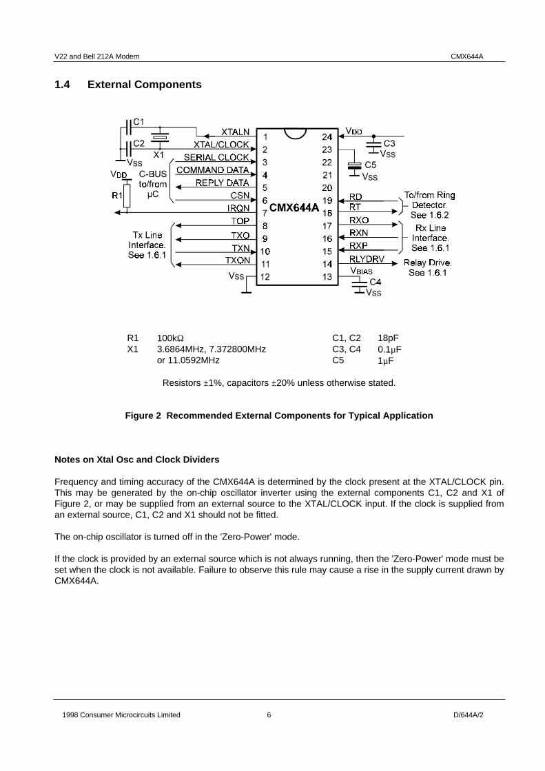
1.4 External Components
R1 100kΩ C1, C2 18pFX1 3.6864MHz, 7.372800MHz
or 11.0592MHzC3, C4C5
0.1µF1µF
Resistors ±1%, capacitors ±20% unless otherwise stated.
Figure 2 Recommended External Components for Typical Application
Notes on Xtal Osc and Clock Dividers
Frequency and timing accuracy of the CMX644A is determined by the clock present at the XTAL/CLOCK pin.This may be generated by the on-chip oscillator inverter using the external components C1, C2 and X1 ofFigure 2, or may be supplied from an external source to the XTAL/CLOCK input. If the clock is supplied froman external source, C1, C2 and X1 should not be fitted.
The on-chip oscillator is turned off in the 'Zero-Power' mode.
If the clock is provided by an external source which is not always running, then the 'Zero-Power' mode must beset when the clock is not available. Failure to observe this rule may cause a rise in the supply current drawn byCMX644A.

V22 and Bell 212A Modem CMX644A
1998 Consumer Microcircuits Limited 7 D/644A/2
1.5 General Description
1.5.1 ‘C-BUS’ Interface
This block provides for the transfer of data and control or status information between the CMX644A’s internalregisters and the µC over the ‘C-BUS’ serial bus. Each transaction, see Figure 3, consists of a single RegisterAddress byte sent from the µC which may be followed by a single data byte sent from the µC to be written intoone of the CMX644A’s Write Only Registers, or a single byte of data read out from one of the CMX644A’sRead Only Registers.
Data sent from the µC on the Command Data line is clocked into the CMX644A on the rising edge of the SerialClock input. Reply Data sent from the CMX644A to the µC is valid when the Serial Clock is high. The interfaceis compatible with the most common µC serial interfaces such as SCI, SPI and Microwire, and may also beeasily implemented with general purpose µC I/O pins controlled by a simple software routine. See section1.7.1 and Figure 9 for detailed ‘C-BUS’ timing requirements.
Figure 3 ‘C-BUS’ Transactions

V22 and Bell 212A Modem CMX644A
1998 Consumer Microcircuits Limited 8 D/644A/2
1.5.2 UART
This block connects the µC, via the ‘C-BUS’ interface, to the received data from the PSK Demodulator and tothe transmit data input to the PSK Modulator.
As part of this function, the block can be programmed to convert data to be transmitted from 7 or 8-bit bytes toasynchronous data characters, adding Start and Stop bits and - optionally - a parity bit to the data beforepassing it to the PSK Modulator. Similarly, in the receive direction it can extract data bits from asynchronouscharacters coming from the PSK Demodulator, stripping off the Start and Stop bits and performing an optionalParity check on the received data before passing the result over the ‘C-BUS’ to the µC. Bits 0-5 of the UARTMODE Register control the number of Stop and Data bits and the Parity options for both receive and transmitdirections.
Data to be transmitted should be loaded by the µC into the TX DATA BYTE Register when the Tx Data Readybit (bit 1) of the FLAGS Register goes high. It will then be treated by the Tx UART block in one of two ways,depending on the setting of bit 5 of the UART MODE Register:
If bit 5 of the UART MODE Register is ‘0’ (‘Sync’ mode) then the 8 bits from the TX DATA BYTERegister will be transmitted sequentially LSB (D0) first.
If bit 5 of the UART MODE Register is ‘1’ (‘Async’ mode) then the 7 or 8 bits will be transmitted asasynchronous data characters according to the following format:
One Start bit (Space).
7 or 8 Data bits from the TX DATA BYTE Register (D0-D6 or D0-D7) as determined by bit 0of the UART MODE Register. LSB (D0) transmitted first.
Optional Parity bit (even or odd parity) as determined by bits 1 and 2 of the UART MODERegister.
Zero, One or Two Stop bits (Mark) as determined by bits 3 and 4 of the UART MODERegister.
In both cases data will only be transmitted if bit 6 of the TX PSK MODE Register is set to ‘1’.
Failure to load the TX DATA BYTE Register with a new value when required will result in bit 2 (TX DATAUNDERFLOW) of the FLAGS Register being set to ‘1’ and a continuous Mark (‘1’) signal will then betransmitted until a new value is loaded into TX DATA BYTE Register.
Figure 4a Transmit UART Function (Async)

V22 and Bell 212A Modem CMX644A
1998 Consumer Microcircuits Limited 9 D/644A/2
Received data from the PSK Demodulator goes into the receive part of the UART block, where it is handled inone of two ways depending on the setting of bit 5 of the UART MODE Register:
If bit 5 of the UART MODE Register is ‘0’ (‘Sync’ mode) then the receive part of the UART block willsimply take 8 consecutive bits from the Demodulator and transfer them to the RX DATA BYTERegister (the first bit going into the D0 position).
If bit 5 of the UART MODE Register is ‘1’ (‘Async’ mode) then the received data output of the PSKDemodulator is treated as asynchronous characters each comprising:
A Start bit (Space).
7 or 8 Data bits as determined by bit 0 of the UART MODE Register. These bits will be placedinto the RX DATA BYTE Register with the first bit received going into the D0 position.
An optional Parity bit as determined by bits 1 and 2 of the UART MODE Register. If Parity isenabled (bit 2 of the UART MODE Register = ‘1’) then bit 7 of the FLAGS Register will be setto ‘1’ if the received parity is incorrect.
Any number of Stop bits (Mark).
Bit 3 (RX DATA READY) of the FLAGS Register will be set to ‘1’ every time a new received value is loadedinto the RX DATA BYTE Register. If the previous contents of the RX DATA BYTE Register had not been readout over the ‘C-BUS’ before the new value is loaded from the UART then bit 4 (RX DATA OVERFLOW) of theFLAGS Register will also be set to ‘1’.
Figure 4b Receive UART Function (Async)

V22 and Bell 212A Modem CMX644A
1998 Consumer Microcircuits Limited 10 D/644A/2
1.5.3 Software Description
Write-only ‘C-BUS’ Registers
REGISTERNAME
HEXADDRESS/COMMAND
BIT 7(D7)
BIT 6(D6)
BIT 5(D5)
BIT 4(D4)
BIT 3(D3)
BIT 2(D2)
BIT 1(D1)
BIT 0(D0)
GENERALRESET
$01 N/A N/A N/A N/A N/A N/A N/A N/A
SET-UP $E0 0RELAYDRIVE
DETECTDET1
DETECTDET0
LOOP-BACK:
L1
LOOP-BACK:
L0
XTALFRQ:
X1
XTALFRQ:
X0TX
TONES $E1TONESEL
TONE /NOTONE
DTMF /MODEMTONES
DTMF /SNGL D3 D2 D1 D0
GAINBLOCKS $E2
TXGAINTG3
TXGAINTG2
TXGAINTG1
TXGAINTG0
RXGAINRG3
RXGAINRG2
RXGAINRG1
RXGAINRG0
TX DATABYTE $E3 D7 D6 D5 D4 D3 D2 D1 D0
UARTMODE
$E4 0 0 SYNC/ASYNC
STOPBITS
B
STOPBITS
A
PARITYENABLE
PARITYODD/EVEN
DATABITS8/7
TX PSKMODE $E7 0
TXONENAB
SCRAMBUNLOCK
SCRAMBENABLE
EQUALET1
EQUALET0
ENABLE HI / LOBAND
RX PSKMODE $E8 0 0
DE-SCRAMBUNLOCK
DE-SCRAMBENABLE
EQUALER1
EQUALER0 ENABLE
HI / LOBAND
IRQMASK BITS $EE
RXPARITY
RINGDETECT DETECT
RX DATAOVER-FLOW
RXDATA
READY
TXDATA
UNDER-FLOW
TXDATA
READY
UN-SCRAMMARK
Write-only Register Descriptions
GENERAL RESET ($01)The reset command has no data attached to it. Application of the GENERAL RESET sets all write-onlyregister bits to ‘0’.
SET-UP Register ($E0)
(Bit 7) Reserved for future use. This bit should be set to ‘0’.
RELAY DRIVE(Bit 6)
This bit controls a low impedance pull-down transistor connected to theRLYDRV pin to assist with the operation of an ‘off-hook relay’. When setto ‘1’ the transistor acts as a pull-down and will sink current. When setto ‘0’ the pin is in a high impedance state.
DETECT DET1 and DET0(Bits 5 and 4)
These 2 bits control the operation of the receiver filter in order to facilitatethe detection of the following signals as shown in the table below:
DET1Bit 5
DET0Bit 4
Required Rx HI/LO Band Setting(Register $E8, Bit 0) Detection
Mode0 0 As required for Rx PSK PSK Carrier0 1 LO = ‘0’ Call Progress1 0 HI = ‘1’ Answer Tone1 1 As required for Rx PSK Detectors OFF
Rx PSK MODE register ENABLE bit should be set to ‘1’ for answertoneand call progress detection.

V22 and Bell 212A Modem CMX644A
1998 Consumer Microcircuits Limited 11 D/644A/2
LOOPBACK L1 and L0(Bits 3 and 2)
These 2 bits control internal signal paths such that loopback tests canbe performed. Function is according to the following table:
L1Bit 3
L0Bit 2
0 0 Normal Device Operation: no loopback.0 1 Local Analogue Loopback: the output of the Tx
gain block is routed to the input of the receivergain block. (The connection between the receiverop-amp and gain block is broken).
1 0 Local Digital Loopback: data is loaded into theTX DATA BYTE register in the usual way via the‘C-BUS’ when indicated by the TX DATA READYflag. This digital data is internally retimed seriallyto the modem bit-rate and is then clocked into thereceiver buffer. When the receiver buffer is full theRX DATA READY flag will be set and the datacan then be read out of RX DATA BYTE registervia the ‘C-BUS’.
1 1 Reserved for future use.
XTAL FRQ X1 and X0(Bits 1 and 0)
These two bits control the internal primary clock dividers to allow for achoice of 3 crystal frequencies. They can also be set to put the deviceinto ‘Zero Power’ mode: in this mode all functions are powersaved,except for the ‘C-BUS’ and the Ring Detector. In ‘Zero Power’ thecrystal oscillator is disabled and the Bias resistor chain is disconnectedfrom the supplies.
Note: When the device is brought out of ‘Zero Power’ mode, thesoftware should allow at least 20ms for the crystal oscillator to re-startand for the Bias capacitor to re-charge, before proceeding with anyfurther device functions. The function is given by the following table:
X1Bit 1
X0Bit 0 Crystal / Mode
0 0 ‘Zero Power’0 1 3.6864MHz crystal1 0 7.3728MHz crystal1 1 11.0592MHz crystal

V22 and Bell 212A Modem CMX644A
1998 Consumer Microcircuits Limited 12 D/644A/2
TX TONES Register ($E1)This register is used to transmit both DTMF and modem progress tones.
TONESEL(Bit 7)
This bit selects the “Answer Tone” frequency in the receive detector. A‘0’ selects 2225Hz and a ‘1’ selects 2100Hz.
TONE/NOTONE(Bit 6)
This bit should be used to begin and end the transmission of tones oncethe required frequency has been programmed. When set to ‘1’ the tonewill be transmitted; when set to ‘0’ a Notone (Bias Voltage) will begenerated.
DTMF/MODEM TONES(Bit 5)
When this bit is set to ‘1’ the device is configured for DTMF. When it isset to ‘0’ the device is configured to transmit modem progress tones.
DTMF/SNGL(Bit 4)
For normal DTMF operation this bit should be set to ‘0’. For testpurposes it can be set to ‘1’ in order to select the tone frequenciesindividually.
The following table shows the settings required for transmitting DTMF (Bit 5 should be set to ‘1’. Bits 6 and 7should be operated as described above).
D3 D2 D1 D0Lower Freq. (Hz)(setting Bit 4 = 0)
Upper Freq. (Hz)(setting Bit 4 = 0)
Keypadsymbol
Single Tone Freq.(Hz)
(setting Bit 4 = 1)0 0 0 0 941 1633 D 16330 0 0 1 697 1209 1 12090 0 1 0 697 1336 2 13360 0 1 1 697 1477 3 14770 1 0 0 770 1209 4 12090 1 0 1 770 1336 5 13360 1 1 0 770 1477 6 14770 1 1 1 852 1209 7 12091 0 0 0 852 1336 8 8521 0 0 1 852 1477 9 8521 0 1 0 941 1336 0 9411 0 1 1 941 1209 * 9411 1 0 0 941 1477 # 9411 1 0 1 697 1633 A 6971 1 1 0 770 1633 B 7701 1 1 1 852 1633 C 852
The following table shows the settings required for transmitting modem progress tones. (Set Bit 4 to ‘0’ andBit 5 to ‘0’. Bits 6 and 7 should be operated as described earlier).
D3 D2 D1 D0 Frequency (Hz) ToneDescription
0 0 0 0 550 Guard0 0 0 1 1300 Calling0 0 1 0 1800 Guard0 0 1 1 2100 Answer0 1 0 0 2225 Answer

V22 and Bell 212A Modem CMX644A
1998 Consumer Microcircuits Limited 13 D/644A/2
GAIN BLOCKS Register ($E2)
Bits 0 to 3 (RG0 to RG3) control the levels of the receiver input gain block according to the following table:
RG3(Bit 3)
RG2(Bit 2)
RG1(Bit 1)
RG0(Bit 0) GAIN (dB)
0 0 0 0 -4.700 0 0 1 -3.460 0 1 0 -2.120 0 1 1 -0.960 1 0 0 0.000 1 0 1 0.870 1 1 0 1.640 1 1 1 2.361 0 0 0 3.081 0 0 1 3.691 0 1 0 4.221 0 1 1 4.761 1 0 0 5.271 1 0 1 5.781 1 1 0 6.211 1 1 1 6.58
The gain should be set in a calibration procedure in order to trim out the effects of any component toleranceswhich may give rise to a variation in the Carrier Detect Threshold levels.
Bits 4 to 7 (TG0 to TG3) control the levels of the transmit path gain block according to the following table:
TG3(Bit 7)
TG2(Bit 6)
TG1(Bit 5)
TG0(Bit 4) GAIN (dB)
0 0 0 0OFF
(o/p at Bias)0 0 0 1 -5.60 0 1 0 -5.20 0 1 1 -4.80 1 0 0 -4.40 1 0 1 -4.00 1 1 0 -3.60 1 1 1 -3.21 0 0 0 -2.81 0 0 1 -2.41 0 1 0 -2.01 0 1 1 -1.61 1 0 0 -1.21 1 0 1 -0.81 1 1 0 -0.41 1 1 1 0.0

V22 and Bell 212A Modem CMX644A
1998 Consumer Microcircuits Limited 14 D/644A/2
TX DATA BYTE Register ($E3)The bytes of data to be transmitted should be loaded into this register. It is double buffered, thus giving theuser up to 8 bit periods to load in the next 8 bits. Each byte represents 4 lots of 2 consecutive bits (dibits) withthe most significant dibit being loaded first (taking Bit 7 of this register as being the most significant). The datais reversed so that it is transmitted least significant dibit first. These dibits represent a transmitted phasechange according to the following table:
Dibit values Phase change Note that the left-hand digit of the dibit is00 + 90° the one occurring first in the data stream01 0° as it enters the modulator portion of the11 + 270° modem after the scrambler.10 + 180°
UART MODE Register ($E4)
(Bit 7 and Bit 6) Reserved for future use. These bits should be set to ‘0’.
SYNC/ASYNC(Bit 5)
When this bit is ‘0’, data will be transmitted and received in normal 8 bitmode without modification.When this bit is ‘1’, data will be transmitted and received with one startbit (‘0’) and 7/8 bits, odd/even parity, 0 or 1 or 2 stop bits according tothe remainder of the bits in this register.
STOP BITS A and B(Bits 4 and 3)
The minimum number of stop bits transmitted after each data byte plusparity is defined by the table below.
Stop BitsA
Stop BitsB
Number ofStop Bits
0 0 00 1 11 0 11 1 2
The receiver does not require any defined number of stop bits.
PARITY ENABLE(Bit 2)
When this bit is ‘1’ an extra bit is added after the data to indicate theparity of that data.When set to ‘0’, parity is disabled. This bit affects both transmitter andreceiver.
PARITY ODD/EVEN(Bit 1)
When this bit is ‘1’ the parity is set odd, and when this bit is ‘0’ the parityis set even.This bit affects both transmitter and receiver.
DATA BITS 8/7(Bit 0)
When this bit is ‘1’ the data is set to transmit and receive 7 bits i.e. bits 0- 6.When this bit is ‘0’ the normal 8 bits of data is programmed.This bit affects both transmitter and receiver.
V22 and Bell 212A Modem CMX644A
1998 Consumer Microcircuits Limited 15 D/644A/2
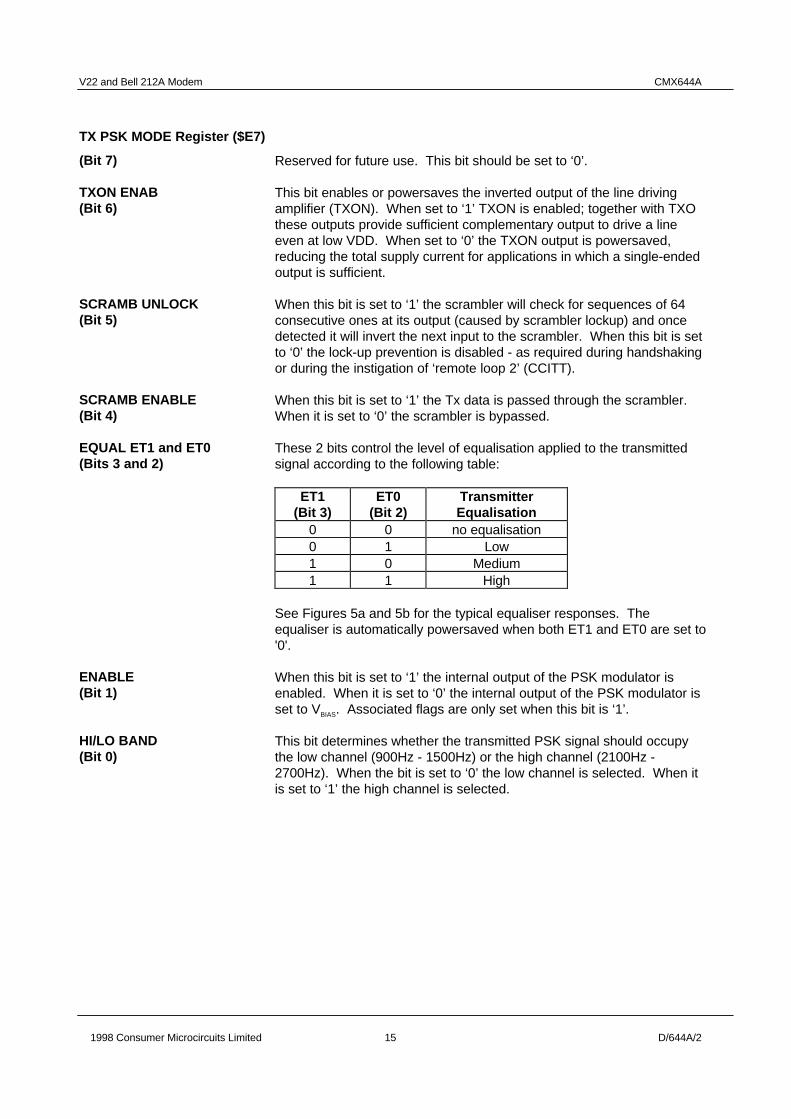
TX PSK MODE Register ($E7)
(Bit 7) Reserved for future use. This bit should be set to ‘0’.
TXON ENAB(Bit 6)
This bit enables or powersaves the inverted output of the line drivingamplifier (TXON). When set to ‘1’ TXON is enabled; together with TXOthese outputs provide sufficient complementary output to drive a lineeven at low VDD. When set to ‘0’ the TXON output is powersaved,reducing the total supply current for applications in which a single-endedoutput is sufficient.
SCRAMB UNLOCK(Bit 5)
When this bit is set to ‘1’ the scrambler will check for sequences of 64consecutive ones at its output (caused by scrambler lockup) and oncedetected it will invert the next input to the scrambler. When this bit is setto ‘0’ the lock-up prevention is disabled - as required during handshakingor during the instigation of ‘remote loop 2’ (CCITT).
SCRAMB ENABLE(Bit 4)
When this bit is set to ‘1’ the Tx data is passed through the scrambler.When it is set to ‘0’ the scrambler is bypassed.
EQUAL ET1 and ET0(Bits 3 and 2)
These 2 bits control the level of equalisation applied to the transmittedsignal according to the following table:
ET1(Bit 3)
ET0(Bit 2)
TransmitterEqualisation
0 0 no equalisation0 1 Low1 0 Medium1 1 High
See Figures 5a and 5b for the typical equaliser responses. Theequaliser is automatically powersaved when both ET1 and ET0 are set to'0'.
ENABLE(Bit 1)
When this bit is set to ‘1’ the internal output of the PSK modulator isenabled. When it is set to ‘0’ the internal output of the PSK modulator isset to VBIAS. Associated flags are only set when this bit is ‘1’.
HI/LO BAND(Bit 0)
This bit determines whether the transmitted PSK signal should occupythe low channel (900Hz - 1500Hz) or the high channel (2100Hz -2700Hz). When the bit is set to ‘0’ the low channel is selected. When itis set to ‘1’ the high channel is selected.

V22 and Bell 212A Modem CMX644A
1998 Consumer Microcircuits Limited 16 D/644A/2
RX PSK MODE Register ($E8)
(Bits 7 and 6) Reserved for future use. These bits should be set to ‘0’.
DE-SCRAMB UNLOCK(Bit 5)
When this bit is set to ‘1’ the de-scrambler will check for sequences of64 consecutive ones at its input and once detected it will invert the nextoutput from the de-scrambler. When this bit is set to ‘0’ the all onesdetection is disabled - it should be set as such until the handshakingsequence is complete.
DE-SCRAMB ENABLE(Bit 4)
When this bit is set to ‘1’ the Rx data is passed through the de-scrambler. When it is set to ‘0’ the de-scrambler is bypassed.
EQUAL ER1 and ER0(Bits 3 and 2)
These 2 bits control the level of equalisation applied to the receivedsignal according to the following table:
ER1(Bit 3)
ER0(Bit 2)
ReceiverEqualisation
0 0 no equalisation0 1 Low1 0 Medium1 1 High
See Figures 5a and 5b for the typical equaliser responses. The equaliser isautomatically powersaved when ET1 and ET0 are set to “no equalisation” (‘0’, ‘0’).
ENABLE(Bit 1)
When this bit is set to ‘1’ the PSK receiver is enabled. When it is set to‘0’ the receiver is disabled. Associated flags are only set when this bit is‘1’.
HI/LO BAND(Bit 0)
This bit determines whether the received PSK signal should be filteredand derived from the low channel (900Hz - 1500Hz) or the high channel(2100Hz - 2700Hz). When this bit is set to ‘0’ the low channel isselected. When it is set to ‘1’ the high channel is selected.

V22 and Bell 212A Modem CMX644A
1998 Consumer Microcircuits Limited 17 D/644A/2
IRQ MASK BITS ($EE)This register is used to control the interrupts (IRQs) as described below:
RX PARITY mask(Bit 7)
When this bit is set to ‘1’ it enables an interrupt that occurs when the RXPARITY flag (Bit 7, FLAGS Register, $EF) changes from ‘0’ to ‘1’ i.e.there is an RX PARITY error. When this bit is ‘0’ the interrupt ismasked.
RING DETECT mask(Bit 6)
When this bit is set to ‘1’ it enables an interrupt that occurs when RINGDETECT CHANGE flag (Bit 6, FLAGS Register, $EF) changes from ‘0’to ‘1’. When this bit is ‘0’ the interrupt is masked.
DETECT mask(Bit 5)
When this bit is set to ‘1’ it enables an interrupt that occurs whenDETECT flag (Bit 5, FLAGS Register, $EF) changes from ‘0’ to ‘1’.When this bit is ‘0’ the interrupt is masked.
RX DATA OVERFLOWmask (Bit 4)
When this bit is set to ‘1’ it enables an interrupt that occurs when RXDATA OVERFLOW flag (Bit 4, FLAGS Register, $EF) changes from ‘0’to ‘1’. When this bit is ‘0’ the interrupt is masked.
RX DATA READY mask(Bit 3)
When this bit is set to ‘1’ it enables an interrupt that occurs when RXDATA READY flag (Bit 3, FLAGS Register, $EF) changes from ‘0’ to ‘1’.When this bit is ‘0’ the interrupt is masked.
TX DATA UNDERFLOWmask (Bit 2)
When this bit is set to ‘1’ it enables an interrupt that occurs when TXDATA UNDERFLOW flag (Bit 2, FLAGS Register, $EF) changes from‘0’ to ‘1’. When this bit is ‘0’ the interrupt is masked.
TX DATA READY mask(Bit 1)
When this bit is set to ‘1’ it enables an interrupt that occurs when TXDATA READY flag (Bit 1, FLAGS Register, $EF) changes from ‘0’ to ‘1’.When this bit is ‘0’ the interrupt is masked.
UNSCRAM MARK mask(Bit 0)
When this bit is set to ‘1’ it enables an interrupt that occurs whenUNSCRAM MARK flag (Bit 0, FLAGS Register, $EF) changes from ‘0’ to‘1’. When this bit is ‘0’ the interrupt is masked.

V22 and Bell 212A Modem CMX644A
1998 Consumer Microcircuits Limited 18 D/644A/2
Read Only ‘C-BUS’ Registers
REGISTERNAME
HEXADDRESS/COMMAND
BIT 7(D7)
BIT 6(D6)
BIT 5(D5)
BIT 4(D4)
BIT 3(D3)
BIT 2(D2)
BIT 1(D1)
BIT 0(D0)
RX DATABYTE $EA D7 D6 D5 D4 D3 D2 D1 D0
TONESDETECT
$EC 0 RINGDETECT
CALLPRGRSSDETECT
CARRIERDETECT
ANSWERDETECT
0 0UN-
SCRAMMARK
DETECT
FLAGS $EFRX
PARITYRING
DETECTCHANGE
DETECTRX DATA
OVER-FLOW
RXDATA
READY
TX DATAUNDER-FLOW
TXDATA
READY
UN-SCRAMMARK
RX DATA BYTE Register ($EA)This register contains the last byte of data received. It is updated every 8 bits at the same time as the RXDATA READY flag is set. The RX DATA BYTE register is double buffered, thus giving the user up to 8 bitperiods to read the data before it is overwritten by the next byte. Each received phase change is decoded into2 bits (a dibit). The incoming dibits fill this register starting at the most significant end (Bits 7 and 6).
Phase change Dibit values Note that the left-hand digit of the dibit will be the more+ 90° 00 significant of the 2 bits when located in this register.
0° 01+ 270° 11+ 180° 10
TONES DETECT Register ($EC)This register provides information as to the presence or absence of various signalling conditions detected bythe receiver. A logic ‘1’ indicates that the signalling condition is present; a logic ‘0’ indicates that it is absent.
(Bit 7) This bit will be set to ‘0’.
RING DETECT(Bit 6)
Indicates the status of the Ring/Line Polarity Reversal Detector circuit.The logic level of this bit represents the level of the internal ‘RINGDETECT’ node (see Figure 1 Block Diagram).
CALL PRGRSS DETECT(Bit 5)
Indicates the detection of call progress tones in the 400Hz to 620Hzband.
CARRIER DETECT(Bit 4)
Indicates the detection of a carrier in the received channel.
ANSWER DETECT(Bit 3)
Indicates the detection of an Answer Tone of 2100Hz or 2225Hz.
(Bits 2 and 1) These bits will be set to ‘0’.
UNSCRAM MARKDETECT (Bit 0)
Indicates the detection of unscrambled binary one in the received datafor a period of time of 160ms.
Note that DETECT bits 5, 4 and 3 are mutually exclusive and are enabled by the setting of the DETECT DET1and DET0 bits (SET-UP Registers Bits 5 and 4). All the DETECT bits in the TONES DETECT register -except for RING DETECT (Bit 6) - require the RX PSK MODE register ENABLE bit to be set to ‘1’.FLAGS Register ($EF)
V22 and Bell 212A Modem CMX644A
1998 Consumer Microcircuits Limited 19 D/644A/2
The flags register is used to indicate when the device requires attention. When a flag becomes set to ‘1’ andits corresponding mask bit is ‘1’ then an interrupt (IRQN) will be generated. Immediately after the flagsregister has been read, all the bits will be reset to ‘0’ and consequently any interrupt will be cleared.
RX PARITY flag(Bit 7)
When this bit is ‘1’ the received parity is in error. When this bit is ‘0’ thereceived parity is correct.
RING DETECT CHANGEflag (Bit 6)
When RING DETECT (TONES DETECT Register, Bit 6) changes state,this bit will be set to ‘1’.
DETECT flag(Bit 5)
When any of the following bits - CALL PRGRSS DETECT, CARRIERDETECT or ANSWER DETECT (TONES DETECT Register Bits 5, 4, 3)- change state, this bit will be set to ‘1’.
RX DATA OVERFLOWflag (Bit 4)
If received data is not read out of the device within the 8-bit window ofRX DATA READY going high, then this bit will be set to ‘1’ to indicate anerror condition.
RX DATA READY flag(Bit 3)
When a full byte of data is received and is available in the RX DATABYTE register, this bit will be set to ‘1’. There is then an 8-bit windowduring which the RX DATA BYTE register must be read.
TX DATA UNDERFLOWflag (Bit 2)
If data is not loaded into the TX DATA BYTE register within the 8-bitwindow of TX DATA READY going high, then this bit will be set to ‘1’ toindicate an error condition.
TX DATA READY flag(Bit 1)
When the Tx data buffer is ready to receive a new byte of data, this bitwill be set to ‘1’. There is then an 8-bit window for the loading of the TXDATA BYTE register.
UNSCRAM MARK flag(Bit 0)
When the UNSCRAM MARK DETECT bit (TONES DETECT RegisterBit 0) changes state, this bit will be set to ‘1’.

V22 and Bell 212A Modem CMX644A
1998 Consumer Microcircuits Limited 20 D/644A/2
0.0E+00
1.0E-04
2.0E-04
3.0E-04
4.0E-04
5.0E-04
6.0E-04
7.0E-04
8.0E-04
9.0E-04
1.0E-03
1.1E-03
1.2E-03
1.3E-03
1.4E-03
1.5E-03
1.6E-03
1.7E-03
1.8E-03
1.9E-03
2.0E-03
600 700 800 900 1000 1100 1200 1300 1400 1500 1600 1700 1800
Frequency (Hz)
Gro
up d
elay
(se
cs)
Lowband
Low
Medium
High
Figure 5a Transmit/Receive Equaliser Responses: Lowband
0.0E+00
1.0E-04
2.0E-04
3.0E-04
4.0E-04
5.0E-04
6.0E-04
7.0E-04
8.0E-04
9.0E-04
1.0E-03
1.1E-03
1.2E-03
1.3E-03
1.4E-03
1.5E-03
1.6E-03
1.7E-03
1.8E-03
1.9E-03
2.0E-03
1800 1900 2000 2100 2200 2300 2400 2500 2600 2700 2800 2900 3000
Frequency (Hz)
Gro
up d
elay
(se
cs)
Highband
Low
Medium
High
Figure 5b Transmit/Receive Equaliser Responses: Highband
The CMX644A utilises two internal equalisers - one is configured for the High Band, the other for the LowBand. The Transmit and Receive paths will be internally switched through the equaliser appropriate totheir HI/LO BAND settings. In the event of both Transmit and Receive paths being set to the same band,both equalisers will be bypassed.

V22 and Bell 212A Modem CMX644A
1998 Consumer Microcircuits Limited 21 D/644A/2
1.6 Application Notes
1.6.1 Line Interface
A line interface circuit is needed to provide dc isolation between the modem and the line, to perform lineimpedance termination, and to set the correct transmit and receive signal levels.
4-Wire Line Interface
Figure 6a shows an interface circuit for use with a 600Ω 4-wire line. The line terminations are provided by R10and R15, while R11 and R13 should be selected to give the desired transmit and receive levels.
When VDD = 5.0V, the gain of the receive input amplifier (R12/R11) should be 6dB (times 2.0) plus whatever
additional gain is required to compensate for the loss of the input transformer. At other values of VDD the
amplifier gain should be multiplied by the ratio VDD/ 5.0.
Thus for R12 = 100kΩ:
R11 = 100kΩ ∗ (5.0/VDD) / (Input transformer loss * 2.0)
where the ‘Input transformer loss’ = (Rx level on 4-wire line) / (level at point A of Figure 6a).
Assuming a transformer loss of about 1dB, R11 should be 47kΩ at VDD = 5.0V, and 68kΩ at 3.3V. The value
of the resistor R11 is optimised for the carrier detect level. Increasing the input gain (by reducing the value ofR11) will improve modem sensitivity.
Note Relay circuit, ac and dc loads and line protection are not shown for clarity.
R10 600Ω R14 100kΩ C10 100nFR11 See text R15 600Ω C11 330pFR12 100kΩ C12 330pFR13 See text C13 100nF
Resistors ±1%, capacitors ±20%.Figure 6a 4-Wire Line Interface Circuit

V22 and Bell 212A Modem CMX644A
1998 Consumer Microcircuits Limited 22 D/644A/2
In the transmit direction, the level on the 4-wire line is determined by the level at the TOP pin, the gain of theOutput Buffer Amplifier, a loss of nominally 6dB due to the line termination resistor R15, and the loss in thetransformer.
The TOP pin signal level is proportional to VDD and is also affected by the setting of the transmitter
programmable gain block.
Assuming that the Tx programmable gain block is set to -2dB (giving a PSK signal level of -4dB wrt 775mVrmsat the TOP pin when VDD = 5.0V) and that there is 1dB loss in the transformer, then:
Tx PSK 4-wire line level = -(4 +6 +1) + 20 ∗ LOG10(2 ∗ R14/R13) + 20 ∗ LOG10(VDD / 5.0) dBm
For example, to generate a nominal Tx FSK line level of -10dBm, R13 should be 180kΩ whenVDD = 5.0V, falling to 120kΩ at 3.3V.
2-Wire Line Interface
Figure 6b shows an interface circuit suitable for connection to a 600Ω 2-wire line. The circuit also shows howa relay may be driven from the RLYDRV pin. Note that when the CMX644A is powered from less than 5.0V,buffer circuitry will be required to drive a 5V relay.
Note: ac and dc loads and line protection are not shown for clarity
R11 See text R15 600Ω C11 330pFR12 100kΩ R16 120kΩ C12 330pFR13 See text R17 100kΩ C13 10nFR14 100kΩ C14 100nF
Resistors ±1%, capacitors ±20%
Figure 6b 2-Wire Line Interface Circuit
This circuit includes a 2-wire to 4-wire hybrid circuit, formed by R11, R15, R16, R17, C13 and the impedanceof the line itself, which ensures that the modem receive input and transmit output paths are both coupledefficiently to the line, while minimising coupling from the modem’s transmit signal into the receive input.The values of R11 and R13 should be calculated in the same way as for the 4-wire interface circuit of Figure6a.

V22 and Bell 212A Modem CMX644A
1998 Consumer Microcircuits Limited 23 D/644A/2
1.6.2 Ring Detector Interface
Figure 7 shows how the CMX644A may be used to detect the large amplitude Ringing signal received at thestart of an incoming telephone call.
The ring signal is usually applied at the subscriber's exchange as an ac voltage inserted in series with one ofthe telephone wires and will pass through either C20 and R20 or C21 and R21 to appear at the top end of R22(point X in Figure 7) in a rectified and attenuated form.
The signal at point X is further attenuated by the potential divider formed by R22 and R23 before being appliedto the CMX644A RD input. If the amplitude of the signal appearing at RD is greater than the input threshold(Vthi) of Schmitt trigger 'A' then the N transistor connected to RT will be turned on, pulling the voltage at RT toVSS by discharging the external capacitor C22. The output of the Schmitt trigger 'B' will then go high, settingbit 6 (RING DETECT) of the TONES DETECT register.
The minimum amplitude ringing signal that is certain to be detected is ( 0.7 + Vthi ∗ [R20 + R22 + R23] / R23 ) ∗ 0.707 Vrms
where Vthi is the high-going threshold voltage of the Schmitt trigger A
With R20 - 22 all 470kΩ as Figure 7, then setting R23 to 68kΩ will guarantee detection of ringing signals of40Vrms and above for VDD over the range 3.0 to 5.5V.
R20,21,22 470kΩ C20,21 0.1µFR23 See text C22 0.33µFR24 470kΩ D1 - 4 1N4004
Resistors ±1%, capacitors ±20%
Figure 7 Ring Signal Detector Interface Circuit

V22 and Bell 212A Modem CMX644A
1998 Consumer Microcircuits Limited 24 D/644A/2
If the time constant of R24 and C22 is large enough then the voltage on RT will remain below the threshold ofthe 'B' Schmitt trigger for the duration of a ring cycle.
The time for the voltage on RT to charge from VSS towards VDD can be derived from the formula
VRT = VDD ∗ [1 - exp(-t/(R24 x C22)) ]
As the Schmitt trigger high-going input threshold voltage (Vthi) has a minimum value of 0.56 x VDD, then theSchmitt trigger B output will remain high for a time of at least 0.821 x R24 x C22 following a pulse at RD.
The values of R24 and C22 given in Figure 7 (470kΩ and 0.33µF) give a minimum RT charge time of100 msec, which is adequate for ring frequencies of 10Hz or above.
Note that the circuit will also respond to a telephone line voltage reversal. If necessary the µC can distinguishbetween a Ring signal and a line voltage reversal by measuring the time that bit 6 of the TONES DETECTregister (RING DETECT) is high.
1.6.3 Software Protocol for Transmitting PSK Data Bytes
In order to transmit PSK data, the following steps should be followed. For clarity, not all bit settings aredescribed here (but HI/LO Band, Equalisation, Guard Tones, Number of Stop Bits etc. should be set asappropriate).
1. Program SETUP register for correct crystal frequency. Wait at least 20ms if device was previously in‘Zero Power’ mode before proceeding.
2. Set Tx Gain Block (GAIN BLOCKS Register $E2) to required gain. Set UART mode.
3. Load first data byte into TX DATA BYTE Register ($E3).
4. Read FLAGS Register ($EF) in order to clear it.
5. Set IRQ MASK BITS Register ($EE Bits 1 and 0) to allow appropriate interrupts (TX DATAUNDERFLOW and TX DATA READY).
6. Set ENABLE bit (TX PSK MODE Register $E7) to ‘1’. The first byte of data will now be transmitted bythe device.
7. Wait for a TX DATA READY generated interrupt (read FLAGS to check and clear the IRQ).
8. Load next TX DATA BYTE.
9. Go to 7.
Note that the transmission should be terminated by setting the ENABLE bit (TX PSK MODE Register) to ‘0’.

V22 and Bell 212A Modem CMX644A
1998 Consumer Microcircuits Limited 25 D/644A/2
1.6.4 Software Protocol for Receiving PSK Data Bytes
1. With the device out of ‘Zero Power’ mode, set up all receiver-related functions: Gain, HI/LO Band,Equalisation, UART mode, etc.
2. Read FLAGS Register ($EF) in order to clear it.
3. Set IRQ MASK BITS Register ($EE Bits 3 and 2) to allow appropriate interrupts (RX DATAOVERFLOW, RX PARITY and RX DATA READY).
4. Set ENABLE bit (RX PSK MODE Register $E8) to ‘1’.
5. Wait for an RX DATA READY generated interrupt (read FLAGS to check and clear the IRQ).
6. Read RX DATA BYTE ($EA).
7. Go to 5.
V22 and Bell 212A Modem CMX644A
1998 Consumer Microcircuits Limited 26 D/644A/2
1.7 Performance Specification
1.7.1 Electrical Performance
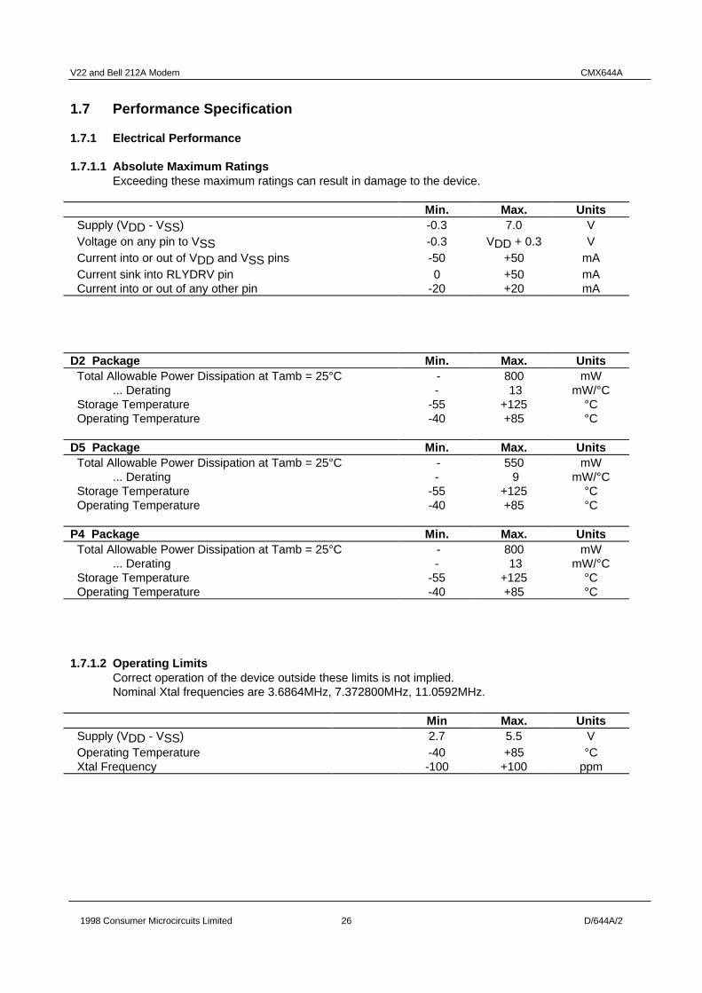
1.7.1.1 Absolute Maximum RatingsExceeding these maximum ratings can result in damage to the device.
Min. Max. Units Supply (VDD - VSS) -0.3 7.0 V Voltage on any pin to VSS -0.3 VDD + 0.3 V Current into or out of VDD and VSS pins -50 +50 mA Current sink into RLYDRV pin 0 +50 mA Current into or out of any other pin -20 +20 mA
D2 Package Min. Max. Units Total Allowable Power Dissipation at Tamb = 25°C - 800 mW ... Derating - 13 mW/°C Storage Temperature -55 +125 °C Operating Temperature -40 +85 °C
D5 Package Min. Max. Units Total Allowable Power Dissipation at Tamb = 25°C - 550 mW ... Derating - 9 mW/°C Storage Temperature -55 +125 °C Operating Temperature -40 +85 °C
P4 Package Min. Max. Units Total Allowable Power Dissipation at Tamb = 25°C - 800 mW ... Derating - 13 mW/°C Storage Temperature -55 +125 °C Operating Temperature -40 +85 °C
1.7.1.2 Operating LimitsCorrect operation of the device outside these limits is not implied.Nominal Xtal frequencies are 3.6864MHz, 7.372800MHz, 11.0592MHz.
Min Max. Units Supply (VDD - VSS) 2.7 5.5 V Operating Temperature -40 +85 °C Xtal Frequency -100 +100 ppm

V22 and Bell 212A Modem CMX644A
1998 Consumer Microcircuits Limited 27 D/644A/2
1.7.1.3 Operating CharacteristicsDetails in this section represent design target values and are not currently guaranteed.
For the following conditions unless otherwise specified:
VDD = 2.7V at Tamb = 25°C and VDD = 3.0V to 5.5V at Tamb = -40 to +85°C.0dBm corresponds to 775mVrms.
Notes Min. Typ. Max. UnitsDC Parameters IDD (‘Zero Power’) 2 - 1 - µA IDD (Operating at VDD = 3.0V) 2 - 3.5 TBD mA
Logic ‘1’ Input Level 5 70% - - VDD
Logic ‘0’ Input Level 5 - - 30% VDD
Logic Input Leakage Current (Vin = 0 to VDD), (excluding XTAL/CLOCK input)
-1.0 - +1.0 µA
Output Logic ‘1’ Level (IOH = 360µA) VDD -0.4 - - V Output Logic ‘0’ Level (IOL = 360µA) - - 0.4 V IRQN O/P ‘Off’ State Current (Vout = VDD) - - 1.0 µA Schmitt trigger input high-going threshold (Vthi) (see Figure 8)
0.56VDD - 0.56VDD V
Schmitt trigger input low-going threshold (Vtlo) (See Figure 8)
0.44VDD -0.6V - 0.44VDD V
Relay Driver pull-down on resistance (VDD = 5.0V)
- 37.0 TBD Ω
Xtal/Clock Input Pulse Width (‘High’ or ‘Low’) 3 40 - - ns Input impedance (at 100Hz) 10 - - MΩ Gain (I/P = 1mV rms at 1kHz) 20 - - dB
AC Parameters
Transmitter (at TOP pin)
Guard Tones Level (below PSK) of 550Hz - -3.0 - dB Level (below PSK) of 1800Hz - -6.0 - dB Frequency Accuracy -0.25 - +0.25 %
PSK Output Transmitted level 1, 4,8 -3.0 -2.0 -1.0 dBm Distortion - 2.0 5.0 %
DTMF Output Transmitted level: high group 1, 4 -2.0 -1.0 0 dBm Twist (high group - low group levels) 4 - 2.0 - dB Distortion 2.0 5 % Frequency Accuracy -0.25 - +0.25 %

V22 and Bell 212A Modem CMX644A
1998 Consumer Microcircuits Limited 28 D/644A/2
Notes Min. Typ. Max. Units Receiver Dynamic Range (VDD = 5.0V) - 45 - dB
Carrier Detect Threshold: Will Decode 1, 6 - - -43 dBm Threshold: Will Not Decode 1, 6 -48 - - dBm Hysteresis 7 - 2.0 - dB Response Time (Delay) - 20 50 ms De-Response Time (Hold) - 20 50 ms
Answer Tone Detector Threshold: Will Decode 1, 6 - - -43 dBm Threshold: Will Not Decode 1, 6 -48 - - dBm Response Time (Delay) - 20 50 ms De-Response Time (Hold) - 20 50 ms
Decode Bandwidth -4 +4 %
Call Progress Detector Effective Bandwidth 400 - 620 Hz Threshold: Will Decode 1, 6 - - -43 dBm Threshold: Will Not Decode 1, 6 -48 - - dBm Response Time (Delay) - 20 50 ms De-Response Time (Hold) - 20 50 ms
Programmable Gain Blocks
Rx Gain Block Nominal Range -4.70 - +6.58 dB (Step Size: see Register Description) Step Accuracy -0.5 - +0.5 dB
Tx Gain Block Nominal Range -5.6 - 0.0 dB Step Size - 0.4 - dB Step Accuracy -0.2 - +0.2 dB
Notes: 1. At VDD = 5.0V only. Signal levels or currents are proportional to VDD.
2. Not including any current drawn from the modem pins by external circuitry.3. Timing for an external input to the CLOCK/XTAL pin.4. Tx Gain Block set to 0dB and measured with a pure tone or DTMF tone pair, without
equalisation.5. Excluding RD, RT and XTAL/CLOCK pins.6. Rx Gain Block nominally set to 0dB but adjusted if necessary for component tolerances.
Measurement point for threshold levels is prior to receive input amplifier circuit (point A onFigure 6a), with external components setting gain to 9dB. Rx Gain Block nominally set to 0dBbut adjusted if necessary for component tolerances. Detector levels measured with a puretone.
7. Hysteresis may be increased, if required, by adding one step (increasing the gain of) to the RxGain Block when a signal is detected and by removing this step when the signal is no longerdetected.
8. Measured with a 511-bit pseudorandom sequence.

V22 and Bell 212A Modem CMX644A
1998 Consumer Microcircuits Limited 29 D/644A/2
0
0 . 5
1
1 . 5
2
2 . 5
3
3 . 5
2 . 5 3 3 . 5 4 4 . 5 5 5 . 5
V d d
V i n
V th i
V t l o
Figure 8 Typical Schmitt Trigger Input Voltage vs. VDD
Tx Timings (See Figure 4a) Notes Min. Typ. Max. UnitsTx Delay from Tx dataloaded (TDEL) TBD ms
Tx Output to Tx reloadsignal (TLOAD) TBD ms
Tx Parity to Tx Underflowflag set (TUFL) TBD ms
Tx Timings (See Figure 4b) Notes Min. Typ. Max. UnitsParity to Rx DataReady flag set (TRDY) TBD ms
V22 and Bell 212A Modem CMX644A
1998 Consumer Microcircuits Limited 30 D/644A/2
1.7.1.3 Operating Characteristics (continued)
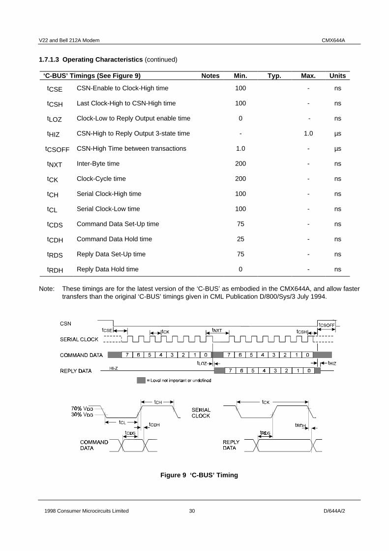
‘C-BUS’ Timings (See Figure 9) Notes Min. Typ. Max. Units
tCSE CSN-Enable to Clock-High time 100 - ns
tCSH Last Clock-High to CSN-High time 100 - ns
tLOZ Clock-Low to Reply Output enable time 0 - ns
tHIZ CSN-High to Reply Output 3-state time - 1.0 µs
tCSOFF CSN-High Time between transactions 1.0 - µs
tNXT Inter-Byte time 200 - ns
tCK Clock-Cycle time 200 - ns
tCH Serial Clock-High time 100 - ns
tCL Serial Clock-Low time 100 - ns
tCDS Command Data Set-Up time 75 - ns
tCDH Command Data Hold time 25 - ns
tRDS Reply Data Set-Up time 75 - ns
tRDH Reply Data Hold time 0 - ns
Note: These timings are for the latest version of the ‘C-BUS’ as embodied in the CMX644A, and allow fastertransfers than the original ‘C-BUS’ timings given in CML Publication D/800/Sys/3 July 1994.
Figure 9 ‘C-BUS’ Timing

V22 and Bell 212A Modem CMX644A
1998 Consumer Microcircuits Limited 31 D/644A/2
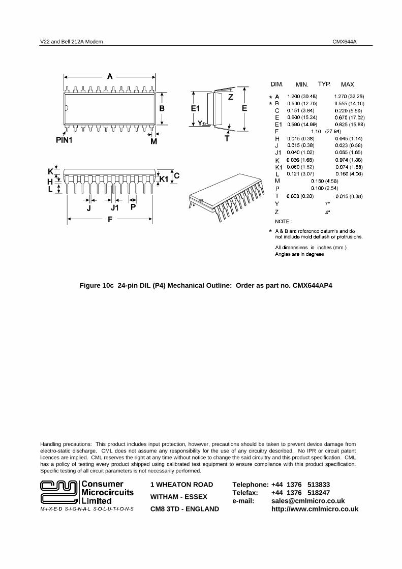
1.7.2 Packaging
Figure 10a 24-pin SOIC (D2) Mechanical Outline: Order as part no. CMX644AD2
Figure 10b 24-pin SSOP (D5) Mechanical Outline: Order as part no. CMX644AD5
V22 and Bell 212A Modem CMX644A
Handling precautions: This product includes input protection, however, precautions should be taken to prevent device damage fromelectro-static discharge. CML does not assume any responsibility for the use of any circuitry described. No IPR or circuit patentlicences are implied. CML reserves the right at any time without notice to change the said circuitry and this product specification. CMLhas a policy of testing every product shipped using calibrated test equipment to ensure compliance with this product specification.Specific testing of all circuit parameters is not necessarily performed.
1 WHEATON ROAD
WITHAM - ESSEX
CM8 3TD - ENGLAND
Telephone: +44 1376 513833Telefax: +44 1376 518247e-mail: [email protected]
http://www.cmlmicro.co.uk
Figure 10c 24-pin DIL (P4) Mechanical Outline: Order as part no. CMX644AP4