CMOS Image Sensors at the Rutherford Appleton Laboratory ...
75
KEK Seminar 9 December 2013, Tsukuba CMOS Image Sensors at the Rutherford Appleton Laboratory and … a bit more Dr Renato Turchetta Rutherford Appleton Laboratory (RAL) Oxfordshire, UK E-mail: [email protected]
Transcript of CMOS Image Sensors at the Rutherford Appleton Laboratory ...

KEK Seminar9 December 2013,
Tsukuba
CMOS Image Sensors at the Rutherford Appleton
Laboratoryand … a bit more
Dr Renato Turchetta
Rutherford Appleton Laboratory (RAL)Oxfordshire, UK
E-mail: [email protected]

Introduction. STFC and some of its detector activities
CMOS image sensors for science
Large area CMOS image sensor Achilles
Lassena
Percival
Ultra-high speed CMOS image sensors PImMS
Kirana
Conclusion
2
Outline

UK Astronomy Technology CentreEdinburgh
Polaris HouseSwindon, Wiltshire
Chilbolton ObservatoryStockbridge, Hampshire
Daresbury LaboratoryDaresbury Science and Innovation CampusWarrington, Cheshire
Rutherford Appleton LaboratoryHarwell Oxford Science and Innovation Campus
Isaac Newton Group of TelescopesLa Palma
Science and Technology Facilities Council
3

International partners
o CERN
o European Southern Observatory ESO
o European Space Agency ESA
o European Synchrotron Radiation Facility ESRF
o Institute Laue-Langevin ILL
STFC in the world4
STFC manage the UK contribution to large scale facilities in the world

Solutions
Transfer
Facilities STFCTechnology
Europracticesoftware
5 Technology

Hexitec ASIC
•80x80 pixels
•Energy Range: 4-200 keV
•1mm CdTe - 500V Bias
•FWHM@60keV = 0.8 +/- 0.2 keV
•(second range 12-600keV)
CdTeor CZT
e-
X-ray
ASIC80x80gold studs
number of electrons= X-ray [eV] / 4.2
2cm
10,000 fps @ rolling shutter
6
Hexitec.
Energy resolving, pixel detector

Hexitec: K-edge Transmission Imaging
Absorption of the I in the tubing and noise of the non-uniform background.
Subtraction to remove background and leave I detail
7
Multi-module, large area sensor
Hexitec. Next.

8 LPD.Large Pixelated Detector
Optimum Energy Range 5 keV – 20 keVSensor Thickness 500 μmPixel Size 500 x 500 μmDynamic Range at 12 keV 105
Inactive area 13%Max. Frame Rate 4.5 MHzMin. Frame Rate 1 MHzGain Factors 1x, 10x, 100xStorage Capacity 512 x 3 Data Output Rate (Mpix) 10GBs
10 KHz
LPD is a high speed (4.5MHz) and high dynamic range (105 @ 12keV) integrating camera system.
Scalable system

9 LPD.Large Pixelated Detector
Custom ASIC in 130 nm CMOS Custom DAQ. 10Gbit links
Custom S/W integrated with machine S/W
The LPD team during the beam test at LCLS this year

CMOS Image Sensor at RAL
10
N+
Br+
N+
Br+ Br+

A
Large area sensor. Stitching.
C
BD
Reticle size is just over 2cm x 2cm ‘stitching’Reticle is subdivided in blocks
A
B
AC A
BD B
C
D
C
D
Sensor size freed from
reticle limitation up
to single sensor per
wafer
Sensors of different
sizes can be
manufactured
56 mm
56 mm
11

12 Transmission Electron Microscopy (TEM). Prior art.
4kx4k CCD camera with phosphor plate
Film
Film: direct detection, very good
resolution, non digital, poor S/N for
weak exposure
CCD with phosphor:
indirect detection
(radiation hardness),
phosphor ruins spatial
resolution, good for
tomography

Direct detection
Good single electron sensitivity
Good MTF and DQE
Radiation resistant
4Kx4K array
16 million pixels
13
CMOS Sensor for TEM

14 Detection of electrons in CMOS
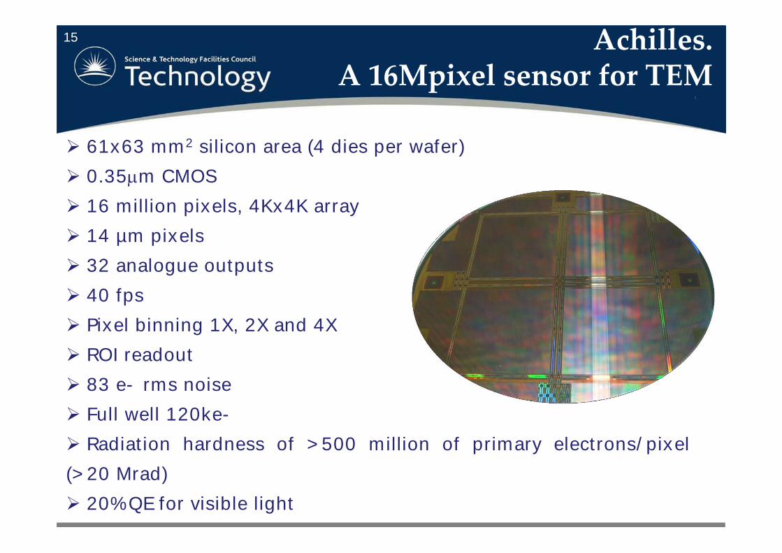
61x63 mm2 silicon area (4 dies per wafer) 0.35m CMOS 16 million pixels, 4Kx4K array 14 µm pixels 32 analogue outputs 40 fps Pixel binning 1X, 2X and 4X ROI readout 83 e- rms noise Full well 120ke- Radiation hardness of >500 million of primary electrons/pixel(>20 Mrad) 20% QE for visible light
15 Achilles.A 16Mpixel sensor for TEM

Courtesy of G. McMullan (LMB, Cambridge, UK)
Adenovirus16

17
Structured scintillators
Mesh in a silicon waferfilled with CsI
‘Artist view’
Photograph

18
Contrast
80
90
100
110
120
130
140
150
350
400
450
500
550
600
200
220
240
260
Scintillator CTF at10LP/mm
Standard A 18%
New Bv1 25um pore
70±10%
New Bv230.8um pore
55±5%
All at 120kV and 3W – noise gives uncertainty to CTF (Contrast Transfer Function) values.
Scint A Scint B
17 lpm @ 10%

19 Wafer‐scale sensor for X‐ray medical imaging
Motivations
Extra-oral dental
with tiling:
Mammography
Chest imaging
Security
...
Guidelines
Wafer-scale sensor
One sensor per 200 mm wafer
3-side buttable 2xN tiling
Radiation hard design
Design for yield

20
Main features
High resolution. 50 µm pixel.
High-speed. Over 30 frames per second at full resolution.
Low noise. 68 e- rms in full frame to give very high sensitivity.
139mmx120mm and 3-side buttable for large area coverage.
High dynamic range. Multiple programmable integration times
Binning x2, x4 and Region-Of-Interest (ROI) readout
Manufactured in 180 nm CMOS Image Sensor process from
TowerJazz Semiconductor

21
Lassena. Floorplan
To the pixel:
3T pixel base with
Low noise, large partially pinned diode
Binning capability

22
68 Full resolution mode (i.e. no binning)
335 Bin 2x2 mode
608 Bin 4x4 mode
112,000 Full resolution mode (i.e. no binning)
1,253,000 Bin 2x2 mode
5,012,000 Bin 4x4 mode
144,000 Full resolution mode (i.e. no binning)
1,374,000 Bin 2x2 mode
5,496,000 Bin 4x4 mode
10.7 Full resolution mode (i.e. no binning)
11.9 Bin 2x2 mode
13.0 Bin 4x4 mode
11.0 Full resolution mode (i.e. no binning)
12.0 Bin 2x2 mode
13.1 Bin 4x4 mode
35 Full resolution mode (i.e. no binning)
70 Bin 2x2 mode
140 Bin 4x4 mode
Quantum efficiency Measured @ 540nm 50%
Lag Negligible
Power supply V 3.3
Number of pads 480 All on one side
Power Consumption (mW) W <2.5 CMOS only
Other
frames per secondReadout speed
Linear full well e-
Optical performance
Rms electronic noise e- rms
Dynamic range (Maximum) bits
Dynamic range (Linear) bits
Maximum full well e-
Lassena. A 6.7Mpixel, wafer‐scale sensor

23
Percival
Pixelated Energy Resolving CMOS Imager,
Versatile and Large

24 Percival target specifications
Low energy X-ray detection <~ 2,000 eV
High efficiency back-side illuminated and direct detection
High resolution 4kx4k on a 25µm pitch
Good single photon sensitivity low noise
High dynamic range, i.e. up to ~ 2*105 photons @ 250 eV high
dynamic range (HDR) pixel --> ~120dB or full well >10 Me-
High frame rate 120 fps
Fully digital

25
HDR pixel
RESET
SELECT
Column
SW0SW1SW2
C0C1C2
Based on overflow
capacitors.
Switches SW0, 1 and 2 are
held ‘almost open’ during
integration

26
Signal path
Pixel Decision block
Sampling stage
MultirampADC
The diode is read first, then the three capacitors
It selects the lowest non saturated value
This value is sampled, as well as the reset value
Both sampled value and reset are converted
ADC conversion over 12 bits. 5 coarse plus 7 fine (plus 1 for over-range)2 bits for gain, as selected by the decision block

Percival sensor floorplan27
Preliminary specifications
16 MPix resolution
120 fps (digital CDS)
High dynamic range (4 gains per
pixel)
12+1bit ADC
15 bits per pixel (2 gain bits + 13
bits)
Digital I/O (LVDS)
60 Gbit/sec continuous data rate
Pixel array4kx4k
@25µm pitch)
28,000 ADCs(7 ADCs per column)
Serialiser and LVDS I/OM
ulti-
leve
l row
con
trol
SP
I and
bia
s ge
nera
tor
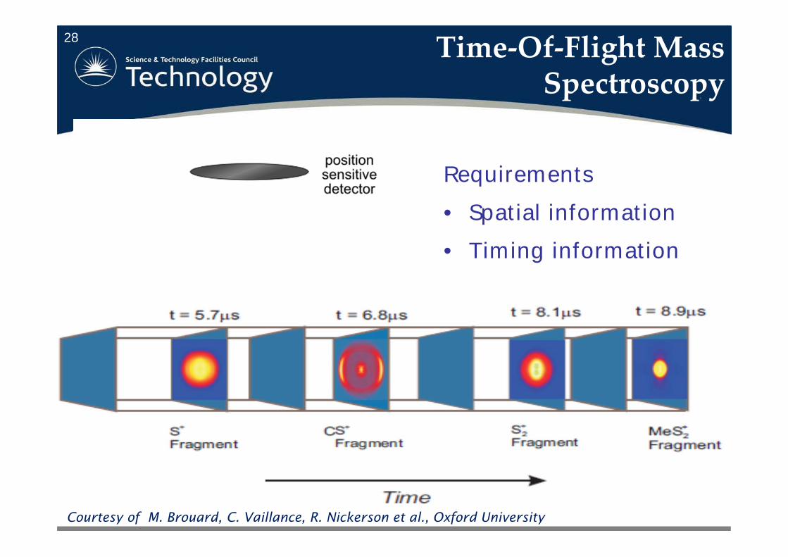
Time‐Of‐Flight Mass Spectroscopy
Courtesy of M. Brouard, C. Vaillance, R. Nickerson et al., Oxford University
28
Requirements• Spatial information• Timing information

29 PImMS. A single particle CMOS Image Sensor.
PImMS – Pixel Imaging Mass Spectrometry

PImMS pixel layout30
Over 600 transistors
per pixel
Modified process
developed with
TowerJazz: deep P-
implant for 100% fill
factor and true CMOS

PImMS172 by 72 pixel array
PImMS2324 by 324 pixel array
31
PImMS family
70 µm x 70 µm pixel size
Time-code resolution= 25 ns (12.5 demonstrated already
on PImMS1)
4 event stored in each pixel
12 bit time-code resolution
Analogue readout of intensity information
Equivalent pixel rate for standard full frame camera
PIMMS USB camera

NOT
N+/Br+ covariance – vertical alignment
N+
Br+
N+
Br+ Br+
32 PImMS. First example of scientific results.

33 (Ultra)‐High speed imaging. Applications
High-speed: 1k to 100kfpsUltra-high speed: >~ 1M fps
Combustion Research Biological/Microscopy Ballistics Mechanics Cavitation Material Research Aerospace Digital Image Correlation PIV

34 (Ultra)‐High speed imaging review
No existing solution

35
Kirana
CMOS for ease of use and readout speed
Start from Tower 180 nm CIS process with
dual gate oxide: 3nm + 10nm
Optimise process for high-speed, high-
efficiency charge transfer
CCD for in-pixel storage

36
Kirana pixel. 1
Photodiode
Memory bank- A vertical entry (VEN)
bank with 10 cells- Ten rows of lateral (LAT)
banks, each with 16 cells- A vertical exit (VEX) bank
with 10 cells
- Total of 180 memory cells

37
Kirana pixel. 2
Highly scalable architecture:- Number of memory cells- Number of pixels

38
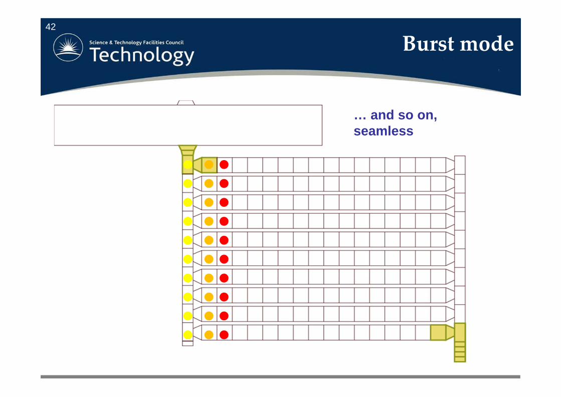
Burst mode
Vertical transfers x10 @ full speed

39
Burst mode
Charge moved into lateral memory bank

40
Burst mode
Ten more vertical transfers

41
Burst mode
Lateral transfer x1 @ full speed / 10
42
Burst mode
… and so on, seamless

43
Burst mode
… and so on, seamless

44
Burst mode
… and so on, seamless

45
Burst mode
… and so on, seamless

46
Burst mode
… and so on, seamless

47
Burst mode
… and so on, seamless

48
Burst mode
… and so on, seamless

49
Burst mode

50
Burst mode
Charge in the vertical exit registers is dumped in the reset node …
… until receipt of the trigger. The status of the memory bank is then frozen and the sensor read out.

51
Continuous mode
Memory bank acting simply like a delay line

52
Continuous mode
Memory bank acting simply like a delay line

53
Continuous mode
Memory bank acting simply like a delay line

54
Continuous mode
Memory bank acting simply like a delay line

55
Continuous mode
Memory bank acting simply like a delay line

56
Continuous mode
Memory bank acting simply like a delay line

57
Continuous mode
Memory bank acting simply like a delay line

58
Continuous mode
Memory bank acting simply like a delay line

59
Continuous mode

60
Continuous mode

61
Continuous mode

62
Continuous mode

63
Continuous mode

64
Continuous mode

65
Continuous mode

66
Sensor floorplan
Pixel array:924 columns
768 rows
CCD drivers (17 lines)For global shutter
operation
Column readout circuitry.
4 rows are read simultaneously
96 valid address on each side; grouped
in 3 banks, individually enabled
42 analogue output channels
@10Mpixel/sec on each side (88 pixels
per amplifier)

67
CCD drivers
Allow multiple level drivers.Signal range: -1V 6V

68
Diode timing
Shutter speed <~ 60 ns

69
Performance summary
Parameter Unit ValuePixel pitch (X) um 30Pixel pitch (Y) um 30
Pixel format (X) 924Pixel format (Y) 768Number of pixels 709,632
Frame rate (burst mode) fps 5,000,000Frame rate (continuous mode) fps 1,180
Pixel rate (burst mode) Pixel/sec 3.5 TPixel rate (continuous mode) Pixel/sec 0.84 G
Noise e- rms <10 e- rmsFull well capacity e- 11,700
Camera gain µV/e- 80Dynamic range >1,170
dB 61.4bit 10.2
Fill Factor 11%
Quantum efficiency Without microlens
2.3% (red)2.2% (blue)
First manufactured on standard epi: 5.5
µm thickness, low resistivity.
New, improved version made on high-res epi and microlenses just received from manufacturing

70
Imaging examples

71
Imaging examples

72
… and also
More CMOS image sensors developed (www.dsc.stfc.ac.uk/cmossensors)
Sensors for Alice at CERN-LHC
Single Photon Avalanche Detector (SPAD) array
Highly Miniaturised Radiation Monitor (HMRM) for ESA
Terahertz detectors

73
Wrap‐up
Broad span of technologies developed at STFC-RAL: detectors, ASIC, DAQ, software, mechanics, cooling, …
Hybrid detectors: Hexitec, LPD, …
CMOS image sensors: focus on science applications, with efficient transfer to industry
Large area sensors up to wafer-scale: Achilles for TEM in production, Lassena for medical imaging, Percival for low-energy X-ray detectors. Ultra-high speed sensors: PIMMS for mass spec, Kiranafor imagingand more!

Colleagues at the Rutherford Appleton Laboratory:
J. Crooks, D. Das, N. Guerrini, B. Marsh, I. Sedgwick, V. Sooden, B. Velagapudi,
M. Hart, M. French, P. Seller, M. Wilson, V. Perera, P. Booker, …
and at collaborating institutes:
R. Henderson, G. McMullan, W. Faruqi (Laboratory of Molecular Biology,
Cambridge)
G. van Hoften (FEI)
M. Brouard, C. Vaillance, R. Nickerson et al. (Oxford University)
W. Chan, K. Taylor (Specialised Imaging)
A. Fenigstein, A. Lahav (TowerJazz Semiconductor)
…
See also www.dsc.stfc.ac.uk/cmossensors
74
Acknowledgements

The last slide75
Questions?
www.dsc.stfc.ac.uk/cmossensors