CMOS Image Sensor(CIS) Image Signal Processor
35
S5C7322X CIS Image Signal Processor Revision 0.0 - of 34 - Nov. 2002 Preliminary 1 Preliminary Specification CMOS Image Sensor(CIS) Image Signal Processor
Transcript of CMOS Image Sensor(CIS) Image Signal Processor

S5C7322X CIS Image Signal Processor
Revision 0.0- of 34 -Nov. 2002
Preliminary
1
Preliminary Specification
CMOS Image Sensor(CIS)Image Signal Processor
S5C7322X CIS Image Signal Processor
Revision 0.0- of 34 -Nov. 2002
Preliminary
2
Documnent TitleCMOS Image Sensor(CIS) Image Signal Processor
Revision HistoryRevision No. History Draft Date Remark
0.0 Initial Draft November 28, 2002 Preliminary
The attached datasheets are provided by SAMSUNG Electronics. SAMSUNG Electronics CO., LTD. reserve the right to change the specifications and
products. SAMSUNG Electronics will answer to your questions about device. If you have any questions, please contact the SAMSUNG branch offices.

S5C7322X CIS Image Signal Processor
Revision 0.0- of 34 -Nov. 2002
Preliminary
3
CMOS Image Sensor(CIS) Image Signal Processor
PROCESS TECHNOLOGY AND PACKAGE
Process : 0.35 um Silicon GATE 4 Metals 2.8 V CMOS Technology(L35)
PKG : 48-ELP-0707
FEATURE
-. Effective Resolution : 640X480, VGA
-. CIS white defect detection and correction
-. Built-in digital clamp function
-. 4-line processing using 3-line memory
-. Luminance/chrominance signal processing of
Bay-array structure
-. Color correction
-. Luminance/chrominance signal processing of
improved SNR
-. Built-in arithmetic function for the AE/AWB
-. Auto exposure
-. Auto white balance
-. Digital Y/Cr/Cb and Sync signals output of 4:2:2
ITU-R.656 format which is 8 bits
-. γ compensation using partial linear interpolation
for each of the degree, R, G and B.
-. Built-in I2C bus interface
-. Built-in self test pattern generator
GENERAL DESCRIPTION
The S5C7322X is highly integrated single chip
CIS(CMOS image sensor) image signal processor,
fabricated by SAMSUNG 0.35um CMOS technology.
The processor is input a digital data of the CIS
output in a camera system which uses a CIS and
produces the luminance signal and the chrominance
signal. It has built-in CalmRISC16 core, the RISC
core for the AE/AWB function.
1) For the signal processing of the camera using the
CIS, the processor separates the luminance signal
and the chrominace signal using built-in 4H delay
line and generates the luminance signal and the
color difference signal by image signal processing. It
calculates intensity using the luminance signal
element for AE which is the main facility of the
camera. It also detects the white color information
and delivers that information to RISC core for AWB.
2) Using the built-in CalmRISC16 core the analog
gain for AE and the coefficient for high-shutter
speed control are calculated. These are output to
CIS and each R/G/B gains for AWB are calculated
to output to RGB Matrix Block.
3) The processor supports the composite image
signal of ITU-R656 format.
4) The processor supports the I2C bus interface.

S5C7322X CIS Image Signal Processor
Revision 0.0- of 34 -Nov. 2002
Preliminary
4
FUNCTIONAL BLOCK DIAGRAM
CISPre-
processor
TG/SSGRISC CORE
S5C7322X
Y/CrCbprocess
Digital
Y/C
(Camera Mode Main OSC)
OSC
ITU.R-656
E2PROM
RGBMATRIX
HSO
VSOI2C
I2C
The preprocess block which accepts the 10-bit CIS outputs performs ADC delay compensation,
digital clamping, CIS defect detection and correction function. This block executes RGB matrix signal
processing for the R/G/B signal generation, luminance signal edge enhancement and chrominance
signal processing, consecutively. And then it outputs the digital Y/C output through output pins. The
oscillator for the above-mentioned camera mode is constructed by main X-TAL only which operates at
24.54MHz.
EACH MODE FREQUENCY
Mode
Item
VGA QVGA QQVGA CIF QCIF
X-tal 24.54MHz
CIS section 12.27MHz 3.06MHz 3.06MHz 3.06MHz 3.06MHz 12.27MHz 3.06MHz
Signal process
section12.27MHz 3.06MHz 3.06MHz 3.06MHz 3.06MHz 12.27MHz 3.06MHz
Y/C Signal
output24.54MHz 6.03MHz 6.03MHz 6.03MHz 6.03MHz 24.54MHz 6.03MHz
I2C BUS 400kHz
CIS
Model S5K433LX
ReadArea
×1 ×1 ×2 ×1 ×2 ×5/3 ×5/3
EffectivePixel
640×480 320×240 320×240 160×120 160×120 352×288 176×144
FrameRate
30 30 30 100 100 30 30

S5C7322X CIS Image Signal Processor
Revision 0.0- of 34 -Nov. 2002
Preliminary
5
ABSOLUTE MAXIMUM RATINGS
Symbol Parameter Rating Unit
VDD DC Supply Voltage -0.3 to 3.8V
VIN DC Input Voltage 3.3V I/O -0.3 to VDD +0.3
IIN DC Input Current ±10 mA
Ilatch Latch-up Current ±200 mA
TSTG Storage Temperature -40 to 125 ℃
RECOMMANDED OPERATING CONDITIONS
Symbol Parameter Rating Unit
VDD DC Supply Voltage 2.55 to 3.05 V
TA Commercial Temperature Range 0 to 70 ℃
1) 0℃ ~ +70℃ 내에서 Function및 AC, DC 특성이 Spec을 만족하도록 함.
ELECTROSTATIC CHARACTERISTICS
ItemElectrostatic Level
UnitPin Number Target Reference Product
Human Body Model
Machine Model
CDM
Latch-Up
ALL
ALL
I-test
Power
±2000V ↑
±200V ↑
±500V ↑
±100㎃ ↑
Vdd max ×1.5 ↑
-
V
V
V
㎃
V

S5C7322X CIS Image Signal Processor
Revision 0.0- of 34 -Nov. 2002
Preliminary
6
RECOMMENDED DC OPERATING CONDITIONS
VDD=2.8±0.25V, TA=0 to 70℃
Item Symbol Condition Min Typ Max Unit Remark
Supply Voltage VDD - 2.55 2.8 3.05
V
Input
voltage
High level VIH - 2.0 - -*1, *2
Low level VIL - - - 0.8
Output
voltage
High level VOH
IOH = -1mA
0.8VDD - -
*3
IOH = -2mA *4
IOH = -4mA *5, *7
IOH = -8mA *6
Low level VOL
IOL = 1mA
- - 0.2VDD
*3
IOL = 2mA *4
IOL = 4mA *5, *7
IOL = 8mA *6
Input
Current
High Level
IIH VIN = VDD
-10 - 10
μA
*1
High level
(Pull-Down)10 30 60 *2
Low Level IIL VIN = VSS -10 - 10 *1, *2
Opreating Current IDD - - 30 - mA -
Static Current ISS - - 100 - mA -
[REMARK]
*1 : #1, #2, #3, #4, #5, #26, #27, #28, #29, #30, #37, #38, #39, #40, #41, #44, #45, #46, #47, #48
*2 : #8, #9, #10, #11, #33, #34, #35
*3 : #36
*4 : #25
*5 : #13, #14
*6 : #12, #15, #16, #17, 20, #21, #22, #23, #24
*7 : #27, #28, #29, #30

S5C7322X CIS Image Signal Processor
Revision 0.0- of 34 -Nov. 2002
Preliminary
7
AC CHARACTERISTICS
VSS = 0V, VDD = 2.8V±0.25, Ta=0∼70℃
Item Signal SymbolCharacteristics
Unit RemarkMin Typ Max
Input Data Setup Time DIN9~DIN0 Tsu 5 - - nsVDD=2.8V±0.25
Ta=0~70℃
Input Data Hold Time DIN9~DIN0 Thd 5 - 50 nsVDD=2.8V±0.25
Ta=0~70℃
CLK
DIN9~0
Thd Tsu
Item Signal SymbolCharacteristics
Unit RemarkMin Typ Max
Output Data Delay Time YC9~YC0 Tdly 0.5 - 3 nsVDD=2.8V±0.25
Ta=0~70℃
VCK
YC9~0
Tdly

S5C7322X CIS Image Signal Processor
Revision 0.0- of 34 -Nov. 2002
Preliminary
8
PIN CONFIGURATION
S5C7322X17
18
19
20
21
13
22
14
15
16
1 2 3 4 5 6 7 8 9 10 11 12
36 35 34 33 32 31 30 29 28 27 26 25
23
24
48
47
42
41
40
39
38
46
37
45
44
43
PCK
VSI
XTAL
RSTN
HSI
VSS
TST2
SCE
VCK
TST1
VDD
TST0
VSO
HSO
YCO0
YCO1
YCO2
VDD
VSS
YCO3
YCO4
YCO5
YCO6
YCO7
DIN0
DIN1
DIN2
DIN3
DIN4
VSS
VDD
DIN5
DIN6
DIN7
DIN8
DIN9
STRB
MD2
MD1
MD0
VSS
VDD
SDA2
SCL2
SDA1
SCL1
STBY
PROT
BLOCK DIAGRAM
PRE-
PROCES
S
4 LINE
PROCES
S
RGB
MATRI
X
EDGE
ENHANC
E
COLOR
MATRIX
AE/
AWB
FORMATTE
R
CPU
TG
1 2 3 4 5 6 7 8 9 10 11 12
PCK
VSI
XTAL
RSTN
HSI
VSS
TST2
SCE
VCK
TST1
VDD
TST0
17
18
19
20
21
13
22
14
15
16
23
24
VSO
HSO
YCO0
YCO1
YCO2
VDD
VSS
YCO3
YCO4
YCO5
YCO6
YCO7
36 35 34 33 32 31 30 29 28 27 26 25
STRB
MD2
MD1
MD0
VSS
VDD
SDA2
SCL2
SDA1
SCL1
SYBY
PROT
48
47
42
41
40
39
38
46
37
45
44
43
DIN0
DIN1
DIN2
DIN3
DIN4
VSS
VDD
DIN5
DIN6
DIN7
DIN8
DIN9

S5C7322X CIS Image Signal Processor
Revision 0.0- of 34 -Nov. 2002
Preliminary
9
PIN DESCRIPTION
Pin # Name I/O Description
1 PCK I Pixel Clock Input from CMOS Image Sensor
2 VSI I Vertical Sync Input from CMOS Image Sensor
3 HSI I Horizontal Sync Input from CMOS Image Sensor
4 RSTN I Master Reset
5 XTAL I X'tal Input
6 VDD P Power
7 VSS G Ground
8 TST0 I Test Mode Selection 0
9 TST1 I Test Mode Selection 1
10 TST2 I Test Mode Selection 2
11 SCE I Scan Test Path Enable Signal
12 VCK O Main Clock Output for Video Module
13 VSO O Vertical sync Output to Video Module
14 HSO O Horizontal sync Output to Video Module
15 YCO0 O Image Data Output 0 (LSB)
16 YCO1 O Image Data Output 1
17 YCO2 O Image Data Output 2
18 VDD P Power
19 VSS G Ground
20 YCO3 O Image Data Output 3
21 YCO4 O Image Data Output 4
22 YCO5 O Image Data Output 5
23 YCO6 O Image Data Output 6
24 YCO7 O Image Data Output 7 (MSB)

S5C7322X CIS Image Signal Processor
Revision 0.0- of 34 -Nov. 2002
Preliminary
10
PIN DESCRIPTION ( Continued )
Pin # Name I/O Description
25 PROT O Protection Signal
26 STBY I Stnad-by Mode ('0' : Stand-by Mode, '1' : Normal Mode)
27 SCL1 I/O Serial Clock Inout1 for I2C Bus
28 SDA1 I/O Serial Address & Data1 Inout for I2C Bus
29 SCL2 I/O Serial Clock Inout2 for I2C Bus
30 SDA2 I/O Serial Address & Data Inout2 for I2C Bus
31 VDD P Power
32 VSS G Ground
33 MD0 I Mode Selection 0
34 MD1 I Mode Selection 1
35 MD2 I Mode Selection 2
36 STRB O Strobe Signal Output to CMOS Image Sensor for Single Frame Capture
37 DIN9 I Data Input from CMOS Image Sensor 9 (MSB)
38 DIN8 I Data Input from CMOS Image Sensor 8
39 DIN7 I Data Input from CMOS Image Sensor 7
40 DIN6 I Data Input from CMOS Image Sensor 6
41 DIN5 I Data Input from CMOS Image Sensor 5
42 VDD P Power
43 VSS G Ground
44 DIN4 I Data Input from CMOS Image Sensor 4
45 DIN3 I Data Input from CMOS Image Sensor 3
46 DIN2 I Data Input from CMOS Image Sensor 2
47 DIN1 I Data Input from CMOS Image Sensor 1
48 DIN0 I Data Input from CMOS Image Sensor 0 (LSB)

S5C7322X CIS Image Signal Processor
Revision 0.0- of 34 -Nov. 2002
Preliminary
11
I2C INTERFACE
The I2C is an industry standard serial interface. The I2C contains a serial two-wire half duplex
interface that features bi-directional operation, master or slave mode. The SDA and SCL are the
bi-directional data and clock pins, respectively. These pins are open-drain type ports and will require
a pull-up resistor to VDD. The image sensor uses the I2C bus to write or read one register byte
per I2C cycle. The I2C bus interface is composed of following parts : START signal, 7-bit slave
device address transmission followed by a read/write bit, an acknowledgement signal from the slave,
8-bit data transfer followed by an acknowledgement signal and STOP signal. The SDA bus line may
only be changed while SCL is low. The data on the SDA bus line is valid on the high-to-low
transition of SCL.
START Signal
When no master device is engaging two bus lines (SCL, SDA), the bus lines are at logical “1”.
A master may initiate communication by sending a START signal which is defined as a high-to-low
transition of SDA while SCL is high. Then, all slaves on the bus wake up to communication.
Slave Address Transmission
After the START signal, the slave address and read/write bit is transmitted by the master. The
7-bit address for the image sensor is 001001b starting with the MSB. The read/write bit following the
7-bit address tells the slave the direction of data transfer. ( 1: read transfer, the slave sends the
data to the master, 0: write transfer, the master sends the data to the slave )
Acknowledgment
Only one slave which has an address sent by the master sends back an acknowledge bit. This is
done by pulling the SDA bus line low at the 9th SCL. If the master receives an acknowledge, it is
said that successful slave addressing has been achieved.
Data Tarnsfer
After successful slave addressing , data transfer is proceeding between the master and the slave
in a direction specified by the read/write bit, the MSB being transferred first. The first data byte of
data is the register address to be read or written. Each data byte is 8bits long and has to followed
by an acknowledge bit, which signals from the receiving device.
STOP Signal
The master can terminate the communication by generating a STOP signal. A STOP signal is
defined as a low-to-high transition of SDA while SCL is high.

S5C7322X CIS Image Signal Processor
Revision 0.0- of 34 -Nov. 2002
Preliminary
12
Write Operation Timing
A. Master transmits a START signal.
B. Master transmits the device slave address with “write” indicated ( binary : 00100010b ).
C. After the device receives slave address, it sends acknowledgment by forcing the SDA bus line
low during the 9th clock.
D. Master transmits the register address.
E. After the device slave receives register address, it sends acknowledgement by forcing the SDA
bus line low during the 9th clock.
F. Master transmits the data to be written at the previously received register address.
G. After the device receives the data to be written, it sends acknowledgement by forcing the SDA
bus line low during the 9th clock.
H. Master transmits STOP signal to end the write cycle.
A6 A5 A4 A3 A2 A1 A0
D7 D6 D5 D4 D3 D2 D1 D0
D7 D6 D5 D4 D3 D2 D1 D0
SCL
SDA
SCL
SCL
SDA
SDA
START WRITE ACK
ACK
ACK STOP
I2C Bus Address
I2C Register Address
I2C Register Data

S5C7322X CIS Image Signal Processor
Revision 0.0- of 34 -Nov. 2002
Preliminary
13
Read Operation Timing
1. Master transmits a START signal
2. Master transmits the S5K711CX slave address with “read” indicated (binary : 00100011b)
3. After S5K711CX slave receives slave address, slave sends acknowledgment by forcing the SDA
bus line low during the 9th clock.
4. Master transmits the register address.
5. After S5K711CX slave receives register address, slave sends acknowledgement by forcing the
SDA bus line low during the 9th clock.
6. S5K711CX transmits the data to be read at the previously received register address.
7. Master does not send an acknowledgment.
8. Master transmits STOP to end the read cycle.
A6 A5 A4 A3 A2 A1 A0
D7 D6 D5 D4 D3 D2 D1 D0
D7 D6 D5 D4 D3 D2 D1 D0
SCL
SDA
SCL
SCL
SDA
SDA
START READ ACK
ACK
NO ACK STOP
I2C Bus Address
I2C Register Address
I2C Register Data

S5C7322X CIS Image Signal Processor
Revision 0.0- of 34 -Nov. 2002
Preliminary
14
SYSTEM FUNCTIONAL DESCRIPTION
PREPROCESS
The preprocess module executes ADC delay adjust, digital clamp, CCD defect detection and
correction. The execution of these function is as follows :
-. ADC Delay Adjust
-. Digital Clamp
-. White Defect Detection
-. Defect Correction
R/G/B MATRIX
The R/G/B matrix is a frequency conversion memory block. In the DVC mode it accomplishes the
function to change a sampling ratio of the output frequency about the input frequency. This
goal is achieved by the address control when we generate the Read Address and the Write Address
using 1H Delay Line which is a input buffer.
-. Adaptive R/G/B Interpolation by 4-Line Processing
-. R/G/B Color Correction
-. Gamma Compensation Using the Partial Linear Approximation
-. Luminance Signal Generation
-. Color Suppression (Highlight, Edge Suppress) Coefficient Generation
EDGE ENHANCEMENT
For the edge enhancement using the output of the luminance signal details tasks following are
performed.
-. Horizontal Edge Enhancement
-. Vertical Edge Enhancement
-. Non-linear Characteristic Process after the Edge Enhancement
-. Noise Slice
-. Level Clip
-. Detail Enhancement
-. High-Light Enhancement Control
-. Gain Control of the luminance
S5C7322X CIS Image Signal Processor
Revision 0.0- of 34 -Nov. 2002
Preliminary
15
COLOR MATRIX
Color difference signals(R-Y,B-Y) for the composite image signal are generated by using R/G/B output.
-. White and Black Adjust
-. Color Difference Signal Generation
-. Hue Adjust
-. Gain Control of the Color Difference Signal
-. High Luminance/Edge Color Suppression
OPTICAL DETECTOR
This block accepts the luminance signal and the R/G/B signal to generate the data for AE(Auto
Exposure) and AWB(Auto White Balance) to the given window area and outputs that data to the RISC
core. And it generates the Window Pulse to display each window area of AE and AWB.
-. 1-Field Luminance Signal Integration for the AE in the Window1 Area
-. 1-Field Luminance Signal Integration for the AE in the Window2 Area
-. Luminance Level Clip Count for the AE in the Window2 Area
-. 1-Field R, G, B Signal Integration for the AWB in the Window Area
RISC CORE
This block receives the data for Auto Exposure(AE) from the optical detector block and generates
Analog Gain and High-Shutter Coefficients from it. These results are output to the CIS. White balance
coefficient is produced from the data for Auto White Balance(AWB) and is output to the Color Matrix
block.
-. Auto Exposure
-. Auto White Balance
-. I2C Bus Interface

S5C7322X CIS Image Signal Processor
Revision 0.0- of 34 -Nov. 2002
Preliminary
16
VIDEO OUTPUT TIMING DIAGRAM
YCrCb Format 1 (Y/Cb/Y/Cr)
HSO
VSO
Y0 Cb0 Y1 Cr0 ··· Y0 Cb0 Y1 Cr0 ··· Y0 Cb0 Y1 Cr0 ···YC
YCrCb Format 2 (Y/Cr/Y/Cb)
HSO
VSO
Y0 Cr0 Y1 Cb0 ··· Y0 Cr0 Y1 Cb0 ··· Y0 Cr0 Y1 Cb0 ···YC

S5C7322X CIS Image Signal Processor
Revision 0.0- of 34 -Nov. 2002
Preliminary
17
YCrCb Format 3 (Cb/Y/Cr/Y)
HSO
VSO
Cb0 Y0 Cr0 Y1 ··· Cb0 Y0 Cr0 Y1 ··· Cb0 Y0 Cr0 Y1 ···YC
YCrCb Format 4 (Cr/Y/Cb/Y)
HSO
VSO
Cr0 Y0 Cb0 Y1 ··· Cr0 Y0 Cb0 Y1 ··· Cr0 Y0 Cb0 Y1 ···YC

S5C7322X CIS Image Signal Processor
Revision 0.0- of 34 -Nov. 2002
Preliminary
18
R/G/B Format 1 (R/G/B)
R : G : B = 5Bits : 6Bits : 5Bits
HSO
VSO
R1/G1
G0/B0 ··· ··· ···YC R0/
G0G1/B1
R0/G0
G0/B0
R1/G1
G1/B1
R0/G0
G0/B0
R1/G1
G1/B1
R[4:0]/G[5:3] G[2:0]/B[4:0]
R/G/B Format 2 (B/G/R)
B : G : R = 5Bits : 6Bits : 5Bits
HSO
VSO
B1/G1
G0/R0 ··· ··· ···YC B0/
G0G1/R1
B0/G0
G0/R0
B1/G1
G1/R1
B0/G0
G0/R0
B1/G1
G1/R1
B[4:0]/G[5:3] G[2:0]/R[4:0]

S5C7322X CIS Image Signal Processor
Revision 0.0- of 34 -Nov. 2002
Preliminary
19
CIS Raw Format
HSO
VSO
D1D0 ··· ··· ···YC D0 D1 D0 D0 D1 D1 D0 D0 D1 D1
6'b000000,D[9:8] D[7:0]

S5C7322X CIS Image Signal Processor
Revision 0.0- of 34 -Nov. 2002
Preliminary
20
REGISTER MAP
Address DATA Default
00
Timing Generator Command
TCMD[7:0]
81
INT_HVS MCK_DIV[1:0] SCK_INV VSO_INV HSO_INV VSI_INV HSI_INV
0 : Use
SYNC
out of
ISP
1 : Use
SYNC
out of
CIS
10 : CIS 8 CLK
division process
→ ISP 4 CLK
division process
01 : CIS 4 CLK
division process
→ ISP 2 CLK
division process
Default : Process
the same CLK
division with CIS
CLK
0 : Red
signal at
the SCK
HIGH
1 : Green
signal at
the SCK
HIGH
0 : Out
VSO
signal
directly
1 : Invert
VSO
signal
0 : Out
HSO
signal
directyl
1 : Invert
HSO
signal
0 : Out
CIS
vertical
signal
directly
1 : Invert
CIS
vertical
signal
0 : Out
CIS
horizontal
signal
directly
1 : Invert
CIS
HORIZON
TAL
SIGNAL
HSO,VSO : H/V signal considered ISP total delay into the
encoder
01
Preproccssor Command
PCOMMAND1[7:0]
00
- HMIR_DEALY[1:0] AD_DELAY[1:0] CLP_EN PTEST THRESH_O
AD Delay reselect
for CIS
10 : AD_DELAY 10
11 : AD_DELAY 00
Default : OUT
AD_DELAY directly
AD clock delay
00 : 1 CLK
01 : 2 CLK
10 : 3 CLK
11 : 4 CLK
0 : Normal
1 : Digital
clamp ON
Defect
generate
enable
0 : OFF
1 : ON
Threshold
value
display
0 : OFF
1 : ON
02
CLAMP_OFFSET
POFFSET[7:0]00
Offset value in CLAMP operation ( -128 ---- 127 : 2's compliment )
03
DUMMY
--
--
04
DUMMY
--
--
05
DUMMY
--
--
06
DUMMY
--
--

S5C7322X CIS Image Signal Processor
Revision 0.0- of 34 -Nov. 2002
Preliminary
21
Address DATA Default
07 DUMMY
08
Detection Window Horizontal Start
PWIN_H_START[7:0]00
Window horizontal start point for defect detection (× 4)
09
Detection Window Horizontal End
PWIN_H_END[7:0]00
Window horizontal end point for defect detection (× 4)
0A
Detection Window Vertical Start
PWIN_V_START[7:0]00
Window vertical start point for defect detection (× 2)
0B
Detection Window Vertical End
PWIN_V_END[7:0]00
Window vertical end point for defect detection (× 2)
0C DUMMY
0D
Horizontal Clamp Start Point
CLP_H_START[7:0]01
Horizontal start point of the optical black region of the CIS (×1)
0E
Vertical Clamp Start Point
CLP_H_START[9:8] CLP_V_START[5:0]
Vertical start point of the optical black region of the CIS (×2)
0F
Threshold Value To Search The Defect Pixel Position
PTHRESH1[7:0]00
Threshold value to judge the white defect
10
CR & CB
CRCB_SEL_ADRS[7:0]
- - - - OUT_SEL[1:0] YC_SEL CRCB_SEL
04- - -
- 00 : ITU656 FORMAT
01 : ITU601 FORMAT
10 : R/G/B FORMAT
11 : CIS OUTPUT
0 : Y
1 : C
0 : CB
1 : CR
11
GAMMA SELECT & PIXEL SEQUENCE CHANGE
RCONTROL_ADRS[7:0]
BW RGB_LIN GAM_SEL RH_CONT RV_CONT RCS_DLY[2:0]
10
0 : BW CIS
1 : Color
CIS
0 : ADM
algorithm
1 : 3-Line
linear
algorithm
Gamma
correction
method
0 : NEW
1 : OLD
Horizontal
pixel
arrangement
0 : SCK
1 : ~SCK
Vertical pixel
arrangement
0 : ID
1 : ~ID
000: -1 MCK 100: 0 MCK
001: -2 MCK 101: 1 MCK
010: -3 MCK 110: 2 MCK
011: -4 MCK 111: 3 MCK

S5C7322X CIS Image Signal Processor
Revision 0.0- of 34 -Nov. 2002
Preliminary
22
Address DATA Default
12
Horizontal Correlation Threshold
RCORTH_H[7:0]
Correlation value among the horizontal pixels for the adaptive RGB interpolation 05
13
Vertical Correlation Threshold
RCORTH_V[7:0]
Correlation value among the vertical pixels for the adaptive RGB interpolation 05
14
R Gain for the R Color Correction
RRR_GAIN[7:0]
R signal gain for the R signal color correction ( X0 ~ X2 ) See address 1CH A4
15
G Gain for the R Color Correction
RRG_GAIN[7:0]
G signal gain for the R signal color correction ( X-1 ~ X1 ) See address 1CH 1D
16
B Gain for the R Color Correction
RRB_GAIN[7:0]
B signal gain for the R signal color correction ( X-1 ~ X1 ) See address 1CH 1F
17
R Gain for the G Color Correction
RGR_GAIN[7:0]
R signal gain for the G signal color correction ( X-1 ~ X1 ) See address 1CH 1E
18
G Gain for the G Color Correction
RGG_GAIN[7:0]
G signal gain for the G signal color correction ( X0 ~ X2 ) See address 1CH B2
19
B Gain for the G Color Correction
RGB_GAIN[7:0]
B signal gain for the G signal color correction ( X-1 ~ X1 ) See address 1CH 21
1A
R Gain for the B Color Correction
RBR_GAIN[7:0]
R signal gain for the B signal color correction ( X-1 ~ X1 ) See address 1CH 24
1B
G Gain for the B Color Correction
RBG_GAIN[7:0]
G signal gain for the B signal color correction ( X-1 ~ X1 ) See address 1CH 23
1C
B Gain for the B Color Correction
RBB_GAIN[7:0]
B signal gain for the B signal color correction ( X0 ~ X2 )
′′′
=
R
G
B
RRR GAIN RRG GAIN RRB GAIN
RGR GAIN RGG GAIN RGB GAIN
RBR GAIN RBG GAIN RBB GAIN
R
G
B
_ _ _
_ _ _
_ _ _
AD
1D
R Coefficient For The Y Signal
RR_COEF[7:0]
R coefficient for the Y signal ( X0 ~ X1 ) See address 1FH 4C
1E
G Coefficient For The Y Signal
RG_COEF[7:0]
G coefficient for the Y signal ( X0 ~ X1 ) See address 1FH 98

S5C7322X CIS Image Signal Processor
Revision 0.0- of 34 -Nov. 2002
Preliminary
23
Address DATA Default
1F
B Coefficient For The Y Signal
RB_COEF[7:0]
B coefficient for the Y signal ( X0 ~ X1 )
※ Y = RR_COEF X R + RG_COEF X G + RB_COEF X B1C
20
Y Highlight Color Suppress Reference
RHLREF[7:0]
Color suppress reference for highlight
Y VALUE
HLREF
VALUE
A0
21
Edge Color Suppression Reference
REGREF[7:0]
Reference value for edge chroma suppress 20
22
C Suppression Gain
RHLFALL_ADRS[7:0]
- - RHLSEL[5] RHLFALL[4:0]
28
- -0 : OFF
1 : ONHigh light color suppress slope
THRESHHOLD(24H)
COLOR GAIN =1 *_C_SUPP-GAIN = 0
*_C_SUPP-GAIN = 63
0 ≤ (HLFALL or EGFALL)/64 < 1.
※ Color suppress coefficient setting <<REGSEL,RHLSEL>>
00 : 6'h3F 01 : Highlight suppress coefficient
10 : Edge suppress coefficient 11 : if HLCS <= EGCS, HLCS else EGCS
23
C Suppress Gain
REGFALL_ADRS[7:0]
- - REGSEL[5] REGFALL[4:0]
28- -
0: OFF
1: ONEdge color suppress slope
24
Gamma Value 1
GM1[7:0]08
Gamma correction coefficient 1 (Output 8-bit value according to the input 23 )
25
Gamma Value 2
GM2[7:0]10
Gamma correction coefficient 2 (Output 8-bit value according to the input 24 )
26
Gamma Value 3
GM3[7:0]20
Gamma correction coefficient 3 (Output 8-bit value according to the input 25 )

S5C7322X CIS Image Signal Processor
Revision 0.0- of 34 -Nov. 2002
Preliminary
24
Address DATA Default
27
Gamma Value 4
GM4[7:0]40
Gamma correction coefficient 4 (Output 8-bit value according to the input 26 )
28
Gamma Value 5
GM57:0]80
Gamma correction coefficient 5 (Output 8-bit value according to the input 27 )
29
Gamma Value 6
GM67:0]00
Gamma correction coefficient 6 (Output 8-bit value according to the input 28 )
2A
Gamma Value 7
GM7[7:0]00
Gamma correction coefficient 7 (Output 8-bit value according to the input 29 )
2B
Gamma Value 8
GM8[7:0]
FF
Gamma correction coefficient 8 (Output 8-bit value according to the input 210 )
2C
Separate Gamma Value For 10-Bit Gamma Value
GM1234H[7:0]
00GM1[9:8] GM2[9:8] GM3[9:8] GM4[9:8]
2D
Separate Gamma Value For 10-Bit Gamma Value
GM5678H[7:0]
1BGM5[9:8] GM6[9:8] GM7[9:8] GM8[9:8]
2E
Pattern Generation Select Signal
PATTERN[7:0]
00
- - PATTERN[1:0] - - - -
01 : color bar
10 : ramp(horizon)
11 : color blue
00 : same as the
preprocessor output
2F DUMMY
102451225612864
512256128
y5
y4
y3
y2
y1
y0
′y0
′y1
′y2
′y 3
′y 4′y5
Input
Output

S5C7322X CIS Image Signal Processor
Revision 0.0- of 34 -Nov. 2002
Preliminary
25
Address DATA Default
30
R Dark Slice
CRDS[7:0]00
Dark slice coefficient of the RED signal (-128≤CRDS≤127)
31
B Dark Slice
CBDS[7:0]00
Dark slice coefficient of the BLUE signal (-128≤CBDS≤127)
32
G Dark Slice
CGDS[7:0]00
Dark slice coefficient of the GREEN signal (-128≤CGDS≤127)
33
RB White Balance
CRBWB[7:0]
- - - - CRWB[9:8] CBWB[9:8]00
- - - - RED white balance BLUE white balance
34
R White Balance
CRWB[7:0]20
White balance coefficient of RED signal (0≤CRWB≤32) ※ SEE ADDR 36
35
B White Balance
CBWB[7:0]20
White balance coefficient of BLUE signal (0≤CBWB≤32) ※ SEE ADDR 36
36
G White Balance
CGWB[7:0]
40
White balance coefficient of GREEN signal (0≤CGWB≤4)
※ R (Black & White) = CRWB×R + CRDS
( 0 ≤ CRWB < 32 , -128 ≤ CRDS ≤ 127 )
G (Black & White) = CGWB×G + CGDS
( 0 ≤ CGWB < 4 , -128 ≤ CGDS ≤ 127 )
B (Black & White) = CBWB×B + CBDS
( 0 ≤ CBWB < 32 , -128 ≤ CBDS ≤ 127 )
37
(R-G) Gain Control for (R-Y)
CRRG[7:0]
59R-G signal coefficient for R-Y signal generation (-1≤CRRG < 1)
※ R-Y = CRRG(R-G) + CRBG(B-G)
B-Y = CBRG(R-G) + CBBG(B-G)
38
(B-G) Gain Control for (R-Y)
CBRG[7:0]D9
B-G signal coefficient for R-Y signal generation (-1≤CBRG < 1) ※ SEE ADDR 37
39
(R-G) Gain Control for (B-Y)
CRBG[7:0]F2
R-G signal coefficient for B-Y signal generation (-1≤CRBG < 1) ※ SEE ADDR 37
3A
(B-G) Gain Control for (B-Y)
CBBG[7:0]72
B-G signal coefficient for B-Y signal generation (-1≤CBBG < 1) ※ SEE ADDR 37

S5C7322X CIS Image Signal Processor
Revision 0.0- of 34 -Nov. 2002
Preliminary
26
Address DATA Default
3B
Horizontal Blank Rising Edge
HBLK_RE[7:0]21
Horizontal-blank rising edge value setting
3C
Horizontal Blank Falling Edge
HBLK_FE[7:0]A1
Horizontal-blank falling edge value setting
3D
Vertical Blank Rising Edge
VBLK_RE[7:0]01
Vertical-blank rising edge value setting
3E
Vertical Blank Falling Edge
VBLK_FE[7:0]E1
Vertical-blank falling edge value setting
3F
Separate H/V Blank Value For 10-Bit H/V Blank Value
HVBLK_RFE[7:0]21
HBLK_RE_ADRS[9:8] HBLK_FE_ADRS[9:8] VBLK_RE_ADRS[9:8] VBLK_FE_ADRS[9:8]
40
(R-Y)_POSI_GAIN
CRYGP[7:0]
80
R-Y positive coefficient for R-Y signal gain control (0 ≤ CRYGP < 2)
※ (R-Y)hue = CRYG(R-Y) + CBYH(B-Y)
(B-Y)hue = CRYH(R-Y) + CBYG(B-Y) G : Gain Control / H : Hue Control
CRYGP CRYHP
CBYHN CBYGN
R-Y
B-Y
CRYGP CRYHP
CBYHP CBYGP
CRYGN CRYHN
CBYHN CBYGN
CRYGN CRYHN
CBYHP CBYGP
41
(R-Y)_NEGA_GAIN
CRYGN[7:0]80
R-Y Negative coefficient for R-Y signal gain control (0 ≤ CRYGN < 2)
42
(B-Y)_HUE_POSI_GAIN
CRYHP[7:0]00
R-Y positive coefficient for B-Y signal hue control (-1 ≤ CRYGP < -1)
43
(B-Y)_HUE_NEGA_GAIN
CRYHN[7:0]00
R-Y Negative coefficient for B-Y signal gain control (-1 ≤ CRYGP < 1)
44
(B-Y)_POSI_GAIN
CBYGP[7:0]80
B-Y positive coefficient for B-Y signal gain control (0 ≤ CBYGP < 2)

S5C7322X CIS Image Signal Processor
Revision 0.0- of 34 -Nov. 2002
Preliminary
27
Address DATA Default
45
(B-Y)_NEGA_GAIN
CBYGN[7:0]80
B-Y negative coefficient for B-Y signal gain control (0 ≤ CBYGN < 2)
46
(R-Y)_HUE_POSI_GAIN
CBYHP[7:0]00
B-Y positive coefficient for R-Y signal hue control (-1 ≤ CBYHP < 1)
47
(R-Y)_HUE_NEGA_GAIN
CBYHN[7:0]00
B-Y negative coefficient for R-Y signal hue control (-1 ≤ CBYHN < 1)
48
C GAIN
CGAIN[7:0]80
Color Level Gain : ×0 ~ ×2
49
COLOR HUE FIX CONTROL
CEFFECT_ADRS[7:0]
- - - - - - - CHUE_FIX
00- - - - - - -
1:Gain = 80(hex)
Hue = 0
0: Just read
directrly
4A DUMY
4B DUMY
4C DUMY
4D DUMY
4E DUMY
4F DUMY
50
AERTURE_NON_LINEAR_CONTROL
YNONLIN_ADRS[7:0]
YVAPTBKTH[1:0] YVAPTBKG[1:0] YHAPTBKTH[1:0] YHATPBKG[1:0]
AA
Non-linear control
threshold value of
the vertical edge
enhancement
Non-linear control
gain of the vertical
edge enhancement
Non-linear control
threshold value of
the horizontal edge
enhancement
Non-linear control gain
of the horizontal edge
enhancement
THRESHOLD
GAIN
※SLOPE=1THRESHOLD
[1:0]Value GAIN[1:0] Value
00 00 00 × 0
01 16(1.6%) 01 ×1/4
10 32(3.1%) 10 ×1/2
11 64(6.3%) 11 × 1

S5C7322X CIS Image Signal Processor
Revision 0.0- of 34 -Nov. 2002
Preliminary
28
Address DATA Default
51
Horizontal Edge Enhancement Control
YHAPGP[7:0]
- YAPTGAIN_H[1:0] YHAPTGAIN_P[4:0]
50-
High-Frequency Edge
Enhancement Filter(HHAP)
Gain Coefficient
Horizontal Positive Edge Enhancement Gain :
(X0 ~ X1)
YAPTGAIN_H[1:0] 00 01 10 11
Mode 2 x HHAP(Z) 4 x HHAP(Z) 8 x HHAP(Z) 10 x HHAP(Z)
HHAP(Z) = -1 + 2Z-1 - Z-2
※ For Aperture Filter Characteristics, see address 52 !
52
Vertical Edge Enhancement Control
YVAPGP[7:0]
- YAPTGAIN_L[1:0] VAPTGAIN_P[4:0]
50-
Low-frequency edge
enhancement Filter(HLAP)
Gain Coefficient
Vertical Positive Edge Enhancement Gain:
(X0 ~ X1)
YAPTGAIN_L[1:0] 00 01 10 11
Mode 0 x HLAP(Z) 2 x HLAP(Z) 4 x HLAP(Z) 6 x HLAP(Z)
HLAP(Z) = -1 + 2Z-3 - Z-4
Transfer function of the final edge enhancement filter : HGAP(Z) = ( HGHAP(Z) + HGLAP(Z))
IF (YAPTGAIN_H,YAPTGAIN_L=0000) : HGAP(Z)
ELSE IF (YAPTGAIN_H,YAPTGAIN_L=0001) : HGAP(Z) / 2
ELSE IF (YAPTGAIN_H,YAPTGAIN_L=1100 OR 1011 OR 1101 OR 1110 OR 1111) : HGAP(Z)/8
ELSE : HGAP(Z)/4
53
H_APERTURE_NEGA_GAIN
YHAPGN[7:0]
10- - - YHAPTGN[4:0]
- - - Horizontal Negative-Edge Enhancement Gain (X0 ~ X1)
54
V_APERTURE_NEGA_GAIN
YVAPGN[7:0]
10- - - YVAPTGN[4:0]
- - - Vertical Negative-Edge Enhancement Gain (X0 ~ X1)
55
Highlight Enhancement
YHLCLP[7:0]
0A- - - - YHCLP[3:0]
- - - -YAPTHLCLP[3:0] : Highlight
enhancement clip level : (7 ~ 127)
56
Y Edge Enhancement Clip
YAPTCLP[7:0]
BFEdge enhancement clip level (x2) (0 ~ 510)

S5C7322X CIS Image Signal Processor
Revision 0.0- of 34 -Nov. 2002
Preliminary
29
Address DATA Default
57
Y Highlight enhancement Noise Slice
YHLSC[7:0]
7F- YHLSC[6:0]
- Highlight enhancement noise slice level ( 0~ 127 )
58
Y Edge Enhancement Noise Slice
YAPTSC[7:0]
00- - APTSC[5:0]
- - Edge enhancement noise slice level (0 ~ 63)
59
Detail Enhancer Threshold & Gain
YENHANTH[7:0]
00
- YENHANTH[6:4] → Threshold - YENHANG[1:0] → Gain
-
000 : 0 100 : 80
001 : 32 101 : 96
010 : 48 110 : 112
011 : 64 111 : 128
-
00 : 1
01 : 1.25
10 : 1.5
11 : 1.75
5A
Highlight Enhancement Gain
YHLGAIN[7:0]
10- - - HLGAIN[4:0]
- - - Highlight enhancement gain (x0 ~ x1)
5B
Y White Clip
YWC[7:0]FF
Y White Clip Level
5C
Y Gain
YGAIN[7:0]80
Y Gain : ×0 ~ ×2
5D
Y Group Delay
YGRPDLY[7:0]
10
- - - OZONE_EN YVAPTSEL[3] YGRPDLY[2:0]
- - -
AE/AWB window
pulse enable
0 : OFF
1 : ON
0 : No LPF
used
1 : LPF
used
Y/C group delay match adjust
000:0CK Delay 100:-3CK Delay
001:1CK Delay 101:-3CK Delay
010:2CK Delay 110:-2CK Delay
011:3CK Delay 111:-1CK Delay
60
AE Window1 Horizontal Start
OAEHS_W1[7:0]23
AE window1 horizontal-start point ( x3 ) ( 1 ~ 211 )
61
AE Window1 Horizontal End
OAEHE_W1[7:0]AF
AE window1 horizontal-end point ( x3 ) ( 3 ~ 213 )

S5C7322X CIS Image Signal Processor
Revision 0.0- of 34 -Nov. 2002
Preliminary
30
Address DATA Default
62
AE Window1 Vertical Start
OAEVS_W1[7:0]0F
AE window1 vertical-start point ( x2 )( 1 ~ 237 )
63
AE Window1 Vertical End
OAEVE_W1[7:0]C8
AE window1 vertical-end point ( x2 )( 3 ~ 239 )
64
AE Window2 Horizontal Start
OAEHS_W2[7:0]0A
AE window2 horizontal-start point ( x3 )( 1 ~ 211 )
65
AE Window2 Horizontal End
OAEHE_W2[7:0]C8
AE window2 horizontal-end point ( x3 )( 3 ~ 213 )
66
AE Window2 Vertical Start
OAEVS_W2[7:0]05
AE window2 vertical-start point ( x2 )( 1 ~ 237 )
67
AE Window2 Vertical End
OAEVE_W2[7:0]DC
AE window2 vertical-end point ( x2 )( 3 ~ 239 )
68
AWB Window Horizontal Start
OAWBHS[7:0]37
AWB window horizontal-start point ( x3 )( 1 ~ 211 )
69
AWB Window Horizontal End
OAWBHE[7:0]BE
AWB window horizontal-end point ( x3 )( 3 ~ 213 )
6A
AWB Window Vertical Start
OAWBVS[7:0]14
AWB window vertical-start point ( x2 )( 1 ~ 237 )
6B
AWB Window Vertical End
OAWBVE[7:0]AA
AWB window vertical-end point ( x2 )( 3 ~ 239 )
6C DUMMY
6D DUMMY
6E DUMMY
6F DUMMY
70
AE Y Signal High Threshold
OYH_AE[7:0]FF
Y signal high-threshold value for the AE ( 0 ≤ OYH_AE ≤ 255 )
71
AE Y Signal Low Threshold
OYL_AE[7:0]00
Y signal low-threshold value for the AE ( 0 ≤ OYL_AE ≤ 255 )
S5C7322X CIS Image Signal Processor
Revision 0.0- of 34 -Nov. 2002
Preliminary
31
Address DATA Default
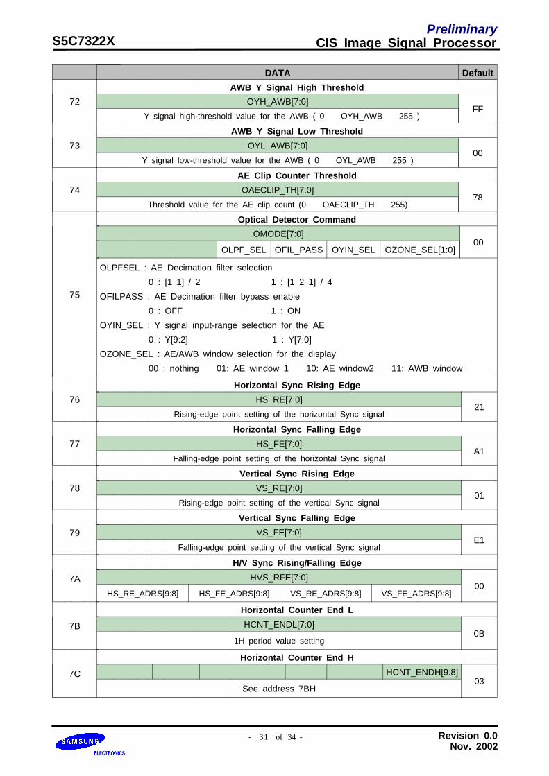
72
AWB Y Signal High Threshold
OYH_AWB[7:0]FF
Y signal high-threshold value for the AWB ( 0 ≤ OYH_AWB ≤ 255 )
73
AWB Y Signal Low Threshold
OYL_AWB[7:0]00
Y signal low-threshold value for the AWB ( 0 ≤ OYL_AWB ≤ 255 )
74
AE Clip Counter Threshold
OAECLIP_TH[7:0]78
Threshold value for the AE clip count (0 ≤ OAECLIP_TH ≤ 255)
75
Optical Detector Command
OMODE[7:0]00
OLPF_SEL OFIL_PASS OYIN_SEL OZONE_SEL[1:0]
OLPFSEL : AE Decimation filter selection
0 : [1 1] / 2 1 : [1 2 1] / 4
OFILPASS : AE Decimation filter bypass enable
0 : OFF 1 : ON
OYIN_SEL : Y signal input-range selection for the AE
0 : Y[9:2] 1 : Y[7:0]
OZONE_SEL : AE/AWB window selection for the display
00 : nothing 01: AE window 1 10: AE window2 11: AWB window
76
Horizontal Sync Rising Edge
HS_RE[7:0]21
Rising-edge point setting of the horizontal Sync signal
77
Horizontal Sync Falling Edge
HS_FE[7:0]A1
Falling-edge point setting of the horizontal Sync signal
78
Vertical Sync Rising Edge
VS_RE[7:0]01
Rising-edge point setting of the vertical Sync signal
79
Vertical Sync Falling Edge
VS_FE[7:0]E1
Falling-edge point setting of the vertical Sync signal
7A
H/V Sync Rising/Falling Edge
HVS_RFE[7:0]00
HS_RE_ADRS[9:8] HS_FE_ADRS[9:8] VS_RE_ADRS[9:8] VS_FE_ADRS[9:8]
7B
Horizontal Counter End L
HCNT_ENDL[7:0]0B
1H period value setting
7C
Horizontal Counter End H
HCNT_ENDH[9:8]03
See address 7BH

S5C7322X CIS Image Signal Processor
Revision 0.0- of 34 -Nov. 2002
Preliminary
32
Address DATA Default
7D
Line Memory Hold
LM_ADDRL[7:0]00
Vertical point of the line memory hold
7E
Line Memory Hold Enable
LM_ADDRH[7:0]
00
- - - - - LM_HOLD_ENABLE LM_ADDR[9:8]
- - - - -
0 : Normal
1 : Shutter replace
enable
See address 7D
7F DUMMY
80
AE Window1 Data H
OAEW1H[7:0]
AE accumulated value of the luminance signal in window1 ( [23:16] )
81
AE Window1 Data M
OAEW1M[7:0]
AE Accumulated value of the luminance signal in window1 ( [15:8] )
82
AE Window1 Data L
OAEW1L[7:0]
AE Accumulated value of the luminance signal in window1 ( [7:0] )
83
AE Window2 Data H
OAEW2H[7:0]
AE accumulated value of the luminance signal in window2 ( [23:16] )
84
AE Window2 Data M
OAEW2M[7:0]
AE Accumulated value of the luminance signal in window2 ( [15:8] )
85
AE Window2 Data L
OAEW2L[7:0]
AE Accumulated value of the luminance signal in window2 ( [7:0] )
86
AE Clip Counter H
OAECLIPH[7:0]
AE clip count value (AECLIPCNT [15:8] )
87
AE Clip Counter L
OAECLIPL[7:0]
AE clip count value (AECLIPCNT [7:0] )
88 DUMMY
89 DUMMY
8A DUMMY
8B DUMMY
8C DUMMY
8D DUMMY
8E DUMMY
8F DUMMY

S5C7322X CIS Image Signal Processor
Revision 0.0- of 34 -Nov. 2002
Preliminary
33
Address DATA Default
90
AWB Window B Data H
OAWBBH[23:16]
Accumulated AWB(B) value in window ( [23:16] )
91
AWB Window B Data M
OAWBBM[15:8]
Accumulated AWB(B) value in window ( [15:8] )
92
AWB Window B Data L
OAWBBL[7:0]
Accumulated AWB(B) value in window ( [7:0] )
93
AWB Window G Data H
OAWBGH[23:16]
Accumulated AWB(G) value in window ( [23:16] )
94
AWB Window G Data M
OAWBGM[15:8]
Accumulated AWB(G) value in window ( [15:8] )
95
AWB Window G Data L
OAWBGL[7:0]
Accumulated AWB(G) value in window ( [7:0] )
96
AWB Window R Data H
OAWBRH[23:16]
Accumulated AWB(R) value in window ( [23:16] )
97
AWB Window R Data M
OAWBRM[15:8]
Accumulated AWB(R) value in window ( [15:8] )
98
AWB Window R Data L
OAWBRL[7:0]
Accumulated AWB(R) value in window ( [7:0] )
99
AWB Counter H
OAWBCNTH[7:0]
Y pixel counter value that is detected in the AWB window (AWB_CNT[15:8])
9A
AWB Counter L
OAWBCNTL[7:0]
Y pixel counter value that is detected in the AWB window (AWB_CNT[7:0])
9B DUMMY
9C DUMMY
9D DUMMY
9E DUMMY
9F DUMMY

S5C7322X CIS Image Signal Processor
Revision 0.0- of 34 -Nov. 2002
Preliminary
34
APPLICATION CIRCUIT DIAGRAM
S5C7322X
PCK
VSI
XTAL
RSTN
HSI
VSS
TST2
SCE
VCK
TST1
VDD
TST0
VSO
HSO
YCO0
YCO1
YCO2
VDD
VSS
YCO3
YCO4
YCO5
YCO6
YCO7
DIN0
DIN1
DIN2
DIN3
DIN4
VSS
VDD
DIN5
DIN6
DIN7
DIN8
DIN9
STRB
MD2
MD1
MD0
VSS
VDD
SDA2
SCL2
SDA1
SCL1
STBY
PROT
Θ
CIS VIDEO
MODULE
E2PROM

S5C7322X CIS Image Signal Processor
Revision 0.0- of 34 -Nov. 2002
Preliminary
35
PACKAGE SPEC