Clock distribution on standing wave with CMOS active ...cj82q861k/... · clock distribution on...
115
CLOCK DISTRIBUTION ON STANDING WAVE WITH CMOS ACTIVE INDUCTOR LOADING Jing Yang A DISSERTATION SUBMITTED IN PARTIAL FULFILLMENT OF THE REQUIREMENTS FOR THE DEGREE OF DOCTOR OF PHILOSOPHY Department of Electrical and Computer Engineering College of Engineering Northeastern University Boston, Massachusetts April 24, 2017 Doctoral Committee Prof. Yong-Bin Kim (Chair) Prof. Nian X. Sun Prof. Fabrizio Lombardi 1
Transcript of Clock distribution on standing wave with CMOS active ...cj82q861k/... · clock distribution on...

CLOCK DISTRIBUTION ON STANDING WAVEWITH CMOS ACTIVE INDUCTOR LOADING
Jing Yang
A DISSERTATION
SUBMITTED IN PARTIAL FULFILLMENT OF THE REQUIREMENTSFOR THE DEGREE OF
DOCTOR OF PHILOSOPHY
Department of Electrical and Computer Engineering
College of Engineering
Northeastern University
Boston, Massachusetts
April 24, 2017
Doctoral Committee
Prof. Yong-Bin Kim (Chair)
Prof. Nian X. Sun
Prof. Fabrizio Lombardi
1

Abstract
Global clock distribution design is becoming an increasingly challenge
task for multi GHz microprocessors. Clock skew and jitter requirement are
becoming more and more stringent as clock frequency increases. For tradi-
tional clock distributions, skew and jitter are proportional to latency, which
is dominated by a series of resistive-capacitance delay and does not scale
with clock period. Moreover, the resistive-capacitance wire-load consumes a
significant amount of power.
As an alternative, resonant clock is applied to reduce dynamic power
and achieve better control of clock skew and jitter. There are three ap-
proaches to create resonant clocks, standing wave, traveling wave, and L-C
tank resonance. Among these approaches, standing wave clock scheme forms
an energy efficient tank that dissipates power only at the parasitic resistance
of the network. Furthermore, standing wave resonance has uniform phase
across the entire clock network, which yields almost zero skew in global clock
distribution. But its voltage and current vary spatially. To overcome the
position-dependent amplitude variation and low output swing issue, passive
inductive loading is proposed, where uniform phase and almost uniform am-
plitude standing wave is realized.
In this thesis, we extend the idea of clock distribution with inductive
loading further by applying CMOS active inductor as inductive loading.
2

Compared to passive inductor design, active inductor can potentially achieve
tunable design with reduced area overhead and high Q value. Moreover, it is
compatible with CMOS technology process and easily integrated into chip-
sets. The thesis first presents a global clock distribution design by generating
standing wave oscillations along inductively loaded micro-strip lines. Trans-
mission line modeling is setting up and analyzed. An improved X-tree clock
topology is employed and cross-coupled pair (CCP) is used to reduce loss
on transmission line. Then standing wave clock distribution with active in-
ductor loading is presented. Three types of active inductor loading on a
standing wave resonant global clock distribution network are proposed. In
the first case, we design a CMOS single cascoded active inductor with tuned
capacitor to increase Q value. The design with a 0.6 nH active inductance
achieves Q of 4630. Applying the active inductor to the entire clock network,
the clock jitter introduced by the active inductor is 0.39 ps. Clock skew is
0.39 ps. In the second case, a novel CMOS differential active inductor with
CCP compensation is proposed. The design has 1.2 nH inductance and Q
of 327. The clock jitter introduced by active inductor loading is 1ps. Clock
skew is 0.52 ps. In the last case, a improved CMOS differential cascoded
active inductor with 1nH inductance and Q 344 is designed. The clock jitter
introduced by active inductor loading is 0.16 ps. Clock skew is 1.95 ps. All
the schemes are based on an improved X-tree clock topology and simulated
in CMOS 28nm technology. The proposed clock distribution schemes greatly
reduce clock skew, jitter, power consumption and chip area.
3

Acknowledgment
I am very grateful to many people for their support and collaboration
through my study in Northeastern University and in my life to date. This
thesis would not have been possible without them. First and foremost, I
would like to thank Professor Yong-bin Kim, my research advisor. He first
raised up my interest in investigating clock distribution using standing wave.
I was enlightened a lot by Professor Kim’s wisdom and ways he solves prob-
lems. Thanks for all the guidance and discussions and challenges as well, all
of which leads to a better understanding of the academic knowledge through
these many years of research and my thesis.
I also would like to thank Professor Nian X. Sun and Professor Fabrizio
Lombardi for serving as my thesis defense committee. Thanks for the time
and effort, the valuable suggestions and generous support. My thanks also
goes to Professor Joseph Ayers, and Professor Kyung Ki Kim for the fantastic
research topic we made together. I learned a lot from this project.
I am deeply indebted to all of my group mates in HPVLSI group, par-
ticularly Inseok Jung, Heungjun Jeon, Jing Lu and Sheng Lin, thanks for
all the discussion and sharing of knowledge during the research. My lab
mates, Donny Yi, Daein Kang, Gyunam Jeon and Yongsuk Choi made life in
HPVLSI lab lots of fun. I really enjoy the accompany and short talks with
your guys. I would also like to thank Rongrong Fu, Chengcheng Jia and
4

Nasibeh Teimouri for all the lunch conversation and tea time. I appreciate
Junxiang Chen’s help for maintaining my desktop while I am remotely doing
my research.
Finally, I would like to thank my parents, it is their support and en-
couragement that I can keep on purchasing the PhD degree. I am so lucky
to be their daughter: I got a fulfillment of love from my parents, I know I
always have a strong support on my back and I can reach the loved one when
in need. I learned the best attitude towards study from them and I know
how people treat their job if they love it. Thanks for all the chatting that I
can share my achievements and frustrations. Thanks for the encouragement
and scarification that I can go for my dream. Thanks for all the snacks and
gifts that I got warmed even when I was alone overseas. I love you my dear
parents.
5

Contents
1 Introduction 15
1.1 Motivations . . . . . . . . . . . . . . . . . . . . . . . . . . . . 15
1.2 Summary of Contributions . . . . . . . . . . . . . . . . . . . . 16
1.3 Outline of Thesis . . . . . . . . . . . . . . . . . . . . . . . . . 18
2 Clock Distribution System 19
2.1 Figure of Merit . . . . . . . . . . . . . . . . . . . . . . . . . . 19
2.1.1 Clock Skew . . . . . . . . . . . . . . . . . . . . . . . . 19
2.1.2 Clock Jitter . . . . . . . . . . . . . . . . . . . . . . . . 20
2.1.3 Power Consumption . . . . . . . . . . . . . . . . . . . 21
2.2 Conventional Clock Distribution . . . . . . . . . . . . . . . . . 22
2.2.1 Tree . . . . . . . . . . . . . . . . . . . . . . . . . . . . 22
2.2.2 Grid . . . . . . . . . . . . . . . . . . . . . . . . . . . . 23
2.2.3 Hybrid . . . . . . . . . . . . . . . . . . . . . . . . . . . 24
2.3 Resonant Clock Distribution . . . . . . . . . . . . . . . . . . . 25
2.3.1 Traveling Wave Resonant . . . . . . . . . . . . . . . . . 26
2.3.2 Standing Wave Resonant . . . . . . . . . . . . . . . . . 27
2.3.3 LC Tank Resonant . . . . . . . . . . . . . . . . . . . . 28
2.3.4 Oscillator Array . . . . . . . . . . . . . . . . . . . . . . 30
3 Transmission Line and Modeling 32
3.1 Background . . . . . . . . . . . . . . . . . . . . . . . . . . . . 32
6

3.2 RLGC Matrix Extract . . . . . . . . . . . . . . . . . . . . . . 38
4 Standing Wave Clock Distribution on Lossy Transmission
Line 40
4.1 Introduction . . . . . . . . . . . . . . . . . . . . . . . . . . . . 40
4.2 Negative Resistance Circuit . . . . . . . . . . . . . . . . . . . 41
4.2.1 Literature Reviews . . . . . . . . . . . . . . . . . . . . 41
4.2.2 Modified Negative Resistance Circuit . . . . . . . . . . 43
4.3 Standing Wave Clocking with Short Ended Load . . . . . . . . 45
4.4 Passive Inductor Loading . . . . . . . . . . . . . . . . . . . . . 51
5 Active Inductor Loading for Transmission Line 58
5.1 Introduction . . . . . . . . . . . . . . . . . . . . . . . . . . . . 58
5.2 Single-Ended Active Inductor . . . . . . . . . . . . . . . . . . 59
5.2.1 General Active Inductor Structure . . . . . . . . . . . . 59
5.2.2 Circuit Examples . . . . . . . . . . . . . . . . . . . . . 66
5.2.3 Improved Single-Ended Active Inductor . . . . . . . . . 71
5.3 Differential Active Inductor . . . . . . . . . . . . . . . . . . . 76
5.3.1 Introduction . . . . . . . . . . . . . . . . . . . . . . . . 76
5.3.2 Improved Topology . . . . . . . . . . . . . . . . . . . . 78
5.3.3 Differential Active Inductor with Cross-Coupled Pair
Compensation . . . . . . . . . . . . . . . . . . . . . . . 81
5.3.4 Cascoded Differential Active Inductor . . . . . . . . . . 85
7

6 Standing Wave Clock Distribution with Active Inductor Load-
ing 91
6.1 Introduction . . . . . . . . . . . . . . . . . . . . . . . . . . . . 91
6.2 Standing Wave Clock Distribution with Single-Ended Active
Inductor . . . . . . . . . . . . . . . . . . . . . . . . . . . . . . 91
6.3 Standing Wave Clock Distribution with Differential Active In-
ductor(CCP) . . . . . . . . . . . . . . . . . . . . . . . . . . . 96
6.4 Standing Wave Clock Distribution with Cascoded Differential
Active Inductor . . . . . . . . . . . . . . . . . . . . . . . . . . 98
6.5 Comparison of Various Standing Wave Clock Distribution . . . 100
7 Conclusion and Future Research 102
7.1 Conclusions . . . . . . . . . . . . . . . . . . . . . . . . . . . . 102
7.2 Future Research Directions . . . . . . . . . . . . . . . . . . . . 103
8

List of Figures
1 Clock skew . . . . . . . . . . . . . . . . . . . . . . . . . . . . . 20
2 Clock jitter . . . . . . . . . . . . . . . . . . . . . . . . . . . . 21
3 Clock tree for global clock distribution . . . . . . . . . . . . . 23
4 Clock grid for global clock distribution . . . . . . . . . . . . . 24
5 Hybrid clock scheme for global clock distribution [27] . . . . . 25
6 Rotary clock distribution network [10] . . . . . . . . . . . . . 27
7 Coupled standing wave resonant clock distribution [4] . . . . . 28
8 Resonant LC tank clock network, with H-tree and grid, induc-
tor, decoupling cap and gain elements are attached to the leaf
of the tree [17] . . . . . . . . . . . . . . . . . . . . . . . . . . . 29
9 Distributed phase locked loops (PLLs) array . . . . . . . . . . 30
10 Distributed VCO array . . . . . . . . . . . . . . . . . . . . . . 31
11 Transmission line RLGC model . . . . . . . . . . . . . . . . . 32
12 Transmission line with ZL loading . . . . . . . . . . . . . . . . 35
13 Standing wave on transmission line with λ length . . . . . . . 38
14 Cross-section of interconnection structure [48,50] . . . . . . . 39
15 Negative resistance circuits . . . . . . . . . . . . . . . . . . . . 41
16 Modified CMOS negative resistance . . . . . . . . . . . . . . . 43
17 Small signal model for the proposed CMOS negative resistance 44
18 Standing wave oscillator with 5 cross-coupled pairs . . . . . . 45
9

19 Simulation result of a single short ended standing wave oscil-
lator with voltage controlled cross-coupled pair . . . . . . . . . 48
20 Standing wave clock distribution with short ended load and
CCP compensation . . . . . . . . . . . . . . . . . . . . . . . . 49
21 Output voltages of various clock nodes . . . . . . . . . . . . . 49
22 Eye-diagram of the clock node next to the short end . . . . . . 50
23 Standing wave oscillator on short-ended and inductive loading
transmission line . . . . . . . . . . . . . . . . . . . . . . . . . 51
24 Standing wave amplitude on short ended and inductive loading
transmission line . . . . . . . . . . . . . . . . . . . . . . . . . 53
25 Standing wave oscillator with inductive loading . . . . . . . . 54
26 Transient waveform of various nodes on SWO with inductive
loading . . . . . . . . . . . . . . . . . . . . . . . . . . . . . . . 55
27 Standing wave clock distribution with inductive load and cross-
coupled pair . . . . . . . . . . . . . . . . . . . . . . . . . . . . 55
28 Output voltages from node closed to the inductor loading . . . 56
29 Skew for the standing wave clock distribution with passive
inductor loading . . . . . . . . . . . . . . . . . . . . . . . . . . 57
30 Jitter for the standing wave clock distribution with passive
inductor loading . . . . . . . . . . . . . . . . . . . . . . . . . . 57
31 Model of ideal single-ended gyrator-C active inductor . . . . . 60
32 Model of lossy single-ended gyrator-C active inductor . . . . . 61
33 The equivalent RLGC model for active inductor . . . . . . . . 62
10

34 Root locus of the lossy gyrator-C active inductor . . . . . . . 64
35 Phase characteristics of the lossy gyrator-C active inductor . . 65
36 Gyrator-C active inductor circuit examples . . . . . . . . . . . 67
37 Small signal model for CS-CD active inductor . . . . . . . . . 68
38 Simplified OTA model for CS-CD active inductor . . . . . . . 70
39 Simplified schematic of Uyanik-Tarim active inductor . . . . . 71
40 Small signal model of Uyanik-Tarim active inductor . . . . . . 72
41 Single-ended active inductor with tunable inductance and Qs 73
42 Simulation result of Uyanik-Tarim active inductor . . . . . . 74
43 Proposed schematic of single-ended active inductor . . . . . . 75
44 Simulation result of the proposed single-ended cascoded active
inductor . . . . . . . . . . . . . . . . . . . . . . . . . . . . . . 76
45 Differential active inductor using differential OTAs . . . . . . 77
46 Differential active inductor circuit examples . . . . . . . . . . 78
47 Schematic of differential active inductor . . . . . . . . . . . . . 79
48 Circuit topology of differential active inductor . . . . . . . . . 79
49 Equivalent circuit of differential active inductor . . . . . . . . 80
50 Small signal model of differential active inductor . . . . . . . . 80
51 Schematic of differential active inductor with CCP . . . . . . 82
52 Half circuit equivalent model of differential active inductor
with CCP . . . . . . . . . . . . . . . . . . . . . . . . . . . . . 82
53 Small signal model of differential active inductor with CCP . . 82
54 Simulation results of differential active inductor with CCP . . 84
11

55 Tuning range of differential active inductor with CCP . . . . . 84
56 THD of differential active inductor with CCP . . . . . . . . . 85
57 Schematic model of cascoded differential active inductor . . . 86
58 Equivalent model of cascoded differential active inductor . . . 86
59 Small signal model of cascoded differential active inductor . . 87
60 Simulation results of cascoded differential active inductor . . . 88
61 Tuning range of cascoded differential active inductor . . . . . 89
62 THD of cascoded differential active inductor . . . . . . . . . . 90
63 Standing wave on transmission line with active inductor loading 91
64 Eye diagram of standing wave on transmission line with active
inductor loading . . . . . . . . . . . . . . . . . . . . . . . . . . 92
65 Global clock distribution with active inductor loading circuit
schematic . . . . . . . . . . . . . . . . . . . . . . . . . . . . . 93
66 Transient simulation results for global clock distribution with
single-ended cascoded active inductor loading . . . . . . . . . 94
67 Eye diagram of global clock distribution with active inductor
loading . . . . . . . . . . . . . . . . . . . . . . . . . . . . . . . 95
68 Global clock distribution with differential active inductor load-
ing and cross-coupled pairs . . . . . . . . . . . . . . . . . . . 96
69 Simulation result of global clock distribution with differential
active inductor loading and CCP . . . . . . . . . . . . . . . . 97
70 Eye diagram of clock distribution with CCP active inductor . 97
12

71 Global clock distribution with cascoded differential active in-
ductor loading . . . . . . . . . . . . . . . . . . . . . . . . . . . 98
72 Simulation result of global clock distribution with cascoded
differential active inductor . . . . . . . . . . . . . . . . . . . . 99
73 Eye diagram of global clock distribution with cascoded differ-
ential active inductor . . . . . . . . . . . . . . . . . . . . . . . 99
13

List of Tables
1 Design parameters of a coupled microstrip transmission line . 39
2 Design parameters of SWO with 5 cross-coupled pairs . . . . . 46
3 Design parameters of the short ended clock distribution in
Figure 20 . . . . . . . . . . . . . . . . . . . . . . . . . . . . . 50
4 Monte Carlo simulation results for passive inductor loading
clock distribution . . . . . . . . . . . . . . . . . . . . . . . . . 57
5 L and Q tunable CMOS active inductor design data, Figure 41 74
6 Design parameters of proposed cascoded single-ended active
inductor . . . . . . . . . . . . . . . . . . . . . . . . . . . . . . 75
7 Design parameters of differential active inductor with CCP . . 83
8 Design parameters of cascoded differential active inductor for
Figure 57 . . . . . . . . . . . . . . . . . . . . . . . . . . . . . 88
9 Design parameters of global clock distribution with single-
ended cascoded active inductor loading . . . . . . . . . . . . . 94
10 Comparison of different loading on standing wave clock distri-
bution network . . . . . . . . . . . . . . . . . . . . . . . . . . 101
14

1 Introduction
1.1 Motivations
Clock distribution design in multi-GHz systems is becoming more and
more challenging. To achieve the desired time margin in synchronous sys-
tems, both clock skew and jitter need to be reduced proportionally to the
clock period. However, for conventional clock distribution, which is typically
buffered clock-tree, the clock skew and jitter are proportional to latency.
Regulating skew and jitter to be less than 10 % of the total clock cycle is
very difficult when clock frequency is above 10GHz.
Furthermore, conventional clock distribution contains a large number
of buffers to balance clock paths and reduce clock skew, the highly toggling
active elements consume a large amount of the total power, as much as 30% -
50% [1] and in extreme cases, up to 70% [2]. High power consumption would
impose more stringent requirements on power supply and heat dissipation.
Ultimately it affects the reliability of the systems.
As an alternative solution, resonant clock distribution is applied to have
better control on clock skew/jitter and reduce the overall power consumption.
Electrical resonance occurs when imaginary parts of impedance cancel out at
a particular frequency known as resonant frequency. Meanwhile the recycling
energy are restored in the on-chip inductors and save the power. According to
this concept, there are three approaches to create resonant clocks: standing
wave [3–9], traveling wave [10–14], and L-C tank resonant [15–21].
15

Standing wave occurs if two harmonic waves of the same frequency and
amplitude travel in opposite direction. If the wire length is properly designed
at integer of quarter wave length [4], the input signal can be delivered along
the line with identical phase but spacial various amplitude. One classic
example of standing wave resonance is by shorting both ends of a half wave
length transmission line. The standing wave amplitude gets its peak at the
center of the line and diminishes to zero at the end of the line. Therefore,
auxiliary circuits such as sense amplifiers are needed to convert it to full
swing, which leads to more power consumption and susceptible to noise.
The low output swing can be improved by using lumped spiral inductor
load instead of shorting the end by wire [7]. The inductor load provides phase
shift and acts as a replacement to part of the transmission line. As a result,
transmission line positions with relatively large standing wave amplitude are
retained, which makes the clock output uniform phase and almost uniform
amplitude.
1.2 Summary of Contributions
In this thesis, we extend the idea of clock distribution with inductive
loading further by applying CMOS active inductor as inductive loading.
Compared to passive inductor design, active inductor can potentially achieve
tunable design with reduced area overhead and high Q value. Moreover, it is
compatible with CMOS technology process and easily integrated into chip-
sets. To get an optimized design, both single-ended and differential active
16

inductor designs are explored with significant efforts to enhance the quality
factor. Issues like transmission loss compensation on clock network when
span is comparable to wave length are discussed. For clock distribution
topologies, most existing standing wave resonant schemes use grid structure,
which is a way to reduce skew, but consume more power and cost large area
overhead. Moreover, the mutual inductance from the grid will be a inter-
ference source to the entire chip. In this thesis, an improved X-tree clock
distribution typology is used, along with the proposed active inductor load-
ing. Detailed designs of 10GHz clock distribution network are presented.
In summary, the purpose of the study is to establish a clock distribution
network that transfer clock signals with a minimum skew and jitter while
consumes less energy and takes up less chip area. The key contributions of
this thesis are:
1. Designed CMOS negative transconductance circuits to compensate trans-
mission line loss for generating standing wave on lossy line
2. Proposed and designed three CMOS active inductor schemes, used
as active inductive load to enhanced the standing wave amplitude on
transmission line
3. Designed global clock distribution scheme with the proposed active
inductor loading to minimize skew, jitter and power consumption
17

1.3 Outline of Thesis
This thesis is organized as follows: Chapter 2 reviews literature of alter-
native clock distribution technique and topologies, lists figure-of-merit and
recent trends in designing global clock. Chapter 3 first explains the trans-
mission line theory basis and the RLGC model. then presents the extracted
RLGC matrices using Cadence transmission line model generator. Chapter 4
focuses on how to generate standing wave reliably on lossy transmission lines.
A improved CMOS cross-coupled pair is proposed to compensate the on-chip
interconnect loss. A 10GHz standing-wave clock distribution design example
with cross-coupled pair compensation is presented. To overcome the spatial
variation in the clock amplitude, Chapter 5 presents the use of active induc-
tor as load on both ends of the mictrostrip. Several improved CMOS active
inductor circuit schemes have been proposed, including singled-ended and
differential active inductors. Chapter 6 reports the entire global clock dis-
tribution network, an improved X-tree clock distribution scheme is proposed
with detailed simulation results. Chapter 7 summarizes work presented in
this thesis and points out potential areas for further studies.
18
2 Clock Distribution System
2.1 Figure of Merit
Most of the digital systems in nowadays, e.g. high-performance micro-
processor, employ synchronous clocking design. High-speed clocks exceeding
GHz are required to globally distributed across the chip. The clock distribu-
tion network are mainly characterized by two aspects: time uncertainty and
power consumption. Clock skew (spatial variation of clock arrival time) and
jitter (clock period from nominal) are two major concern of time uncertainty.
Power usually categorizes into static power and dynamic power.
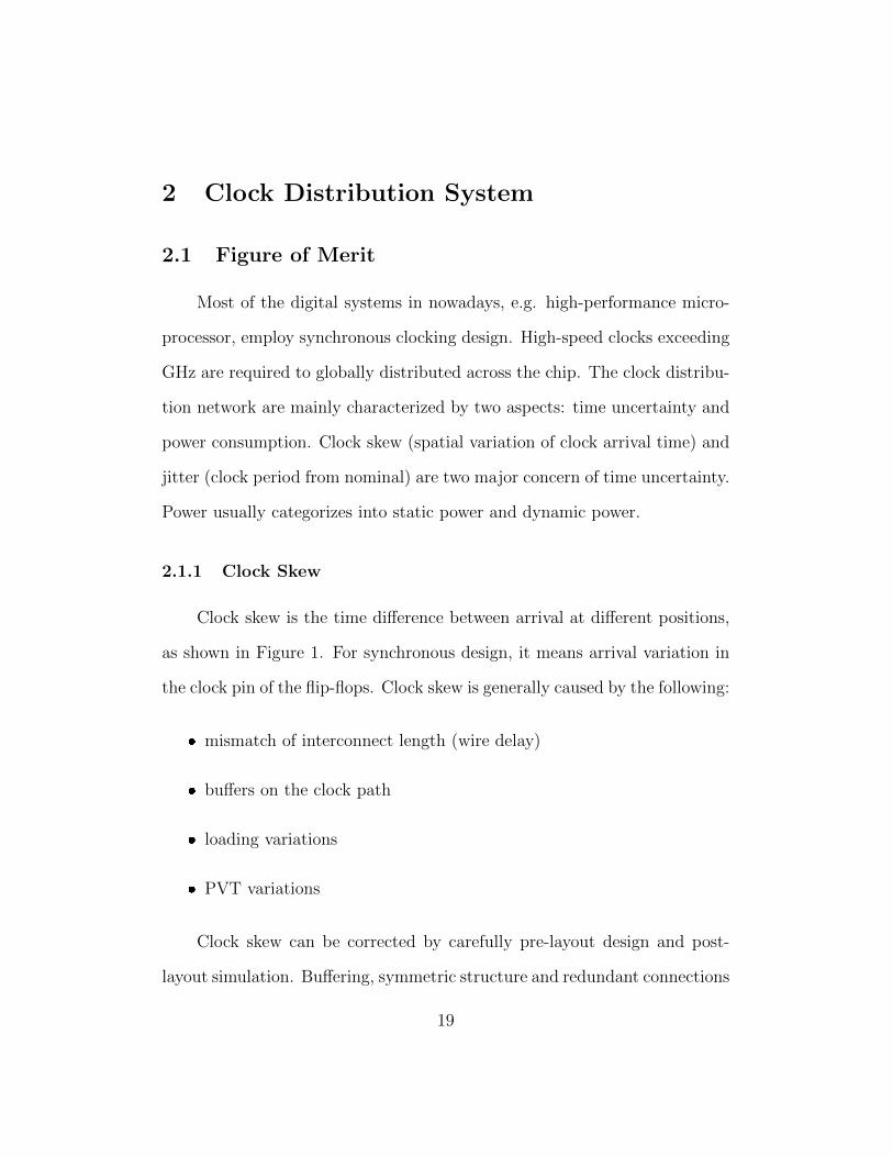
2.1.1 Clock Skew
Clock skew is the time difference between arrival at different positions,
as shown in Figure 1. For synchronous design, it means arrival variation in
the clock pin of the flip-flops. Clock skew is generally caused by the following:
mismatch of interconnect length (wire delay)
buffers on the clock path
loading variations
PVT variations
Clock skew can be corrected by carefully pre-layout design and post-
layout simulation. Buffering, symmetric structure and redundant connections
19

y
x
xtskew
Figure 1: Clock skew
are commonly used to minimize clock skew [22–26].
2.1.2 Clock Jitter
Jitter is defined as period variations at different clock cycles on a clock
node, as shown as in Figure 2. There are two types of jitter: deterministic
and random. Deterministic jitter is caused by interference signals such as
power supply noise, gate switching etc. Random jitter is usually caused by
PVT variations and can be characterized statistically.
In the past, jitter was dominated by the clock source, which is usually
made of an on-chip phase-locked loop (PLL) that multiplies the off-chip clock
reference to the core clock frequency. However, PLL jitter has been scaled
well with technology while the jitter in the clock distribution has not. As
a result, the dominant source of clock jitter for today’s high-performance
microprocessors is the clock distribution.
20

x
y
tclk tclk
tjitter
tclk-tjitter tclk+tjitter
Figure 2: Clock jitter
2.1.3 Power Consumption
Power consumption can be categorized into static power and dynamic
power. Static power consumption refers to the power when there is no cir-
cuit activity, e.g. the leakage from transistors. Dynamic power is power
consumed while the inputs are active, e.g. power consumed when charging
and discharging a capacitive output load. Dynamic power is the main contri-
bution to the overall system power. But as technology scaled to nano meter
design, static power is playing a more and more important role.
The dynamic power Pdyn of digital systems can be expressed as
Pdyn = αCLV2f (1)
where α is switching rate, CL is load capacitance, V is the voltage swing
and f is the clock frequency. For a clock distribution network, the major
21

power consumption comes from the loading on the leaf of the clock network,
which usually is capacitance of the flip-flop clock pins, the loading from the
buffer and wiring capacitance. For modern high speed design, the power
consumption of the clock distribution network can be around 30% to 50% [1]
and in extreme cases can be up to 70% [2] of the entire digital system.
2.2 Conventional Clock Distribution
Conventional clock distribution uses a hierarchical approach to deliver
the clock signal across the entire chip. The global clock distribution network
takes the clock reference and drives the local distribution network with low
skew clocks copies. Typically the global clock topologies can be tree, grid or
hybrid of tree and grid. The local distribution network would contain buffers
to match the loading and equalize the delay from the clock source to the
clock pin of the flip-flops.
2.2.1 Tree
Figure 3 shows some example of global clock distribution using tree
topology, including binary tree and H-tree scheme. The main idea is to
balance the delays of various path by splitting the clock source symmetrically
at each stage. Therefore, multiple clock copies are created. H-tree clock
distribution (Figure 3b) is constructed from perpendicular line segments and
the repeating pattern resembles the letter ”H”. It requires relatively regular
floorplan. In contrast, binary tree (Figure 3a) has less stringent floorplan
22

requirement. The buffer along the tree can be placed closely. Both H-tree
and binary tree provide the flexibility to individually tune the skew along each
path through sizing of the buffers. Additionally, fine-grained clock gating can
be easily achieved by inserting clock gating cells on individual clock branches.
However, due to the various number of flip-flops to be driven at each clock
nodes, it is difficult to balance the path delays and gain closed to zero skews,
especially under various PVT from on chip variation (OCV).
(a) binary clock tree
(b) H-tree
Figure 3: Clock tree for global clock distribution
2.2.2 Grid
Clock grid is popular in high performance high speed microprocessors
using custom methodologies, as shown in Figure 4. In the clock grid architec-
23

ture, multiple copies of the root clock signal are injected into various nodes a
metal mesh. The metal mesh provides paths down to the clock sinks via its
regular mesh routing structure. Due to the cross-linking between the clock
nodes, clock grid is less susceptible to loading variations and has better con-
trol on skew and jitter. On the other hand, clock grids has large capacitive
loads, and hence higher power dissipation and wire usage.
Clock
Figure 4: Clock grid for global clock distribution
2.2.3 Hybrid
As addressed before, clock grid provides a load-independent method of
clock delivering but takes more wiring and routing resources, which results
in high power and area overhead. Clock tree, on the contrary, has relatively
low routing overhead but are sensitive to PVT OCV and hard to balance
between clock nodes. Hybrid clock scheme is a mixture of clock grid and
clock tree to take benefits from each scheme. Various hybrid clock scheme
has been proposed. Figure 5a shows an example when a mesh is used to
24

distribute clocks from a global clock source and the local trees distribute the
clock to local regions. Figure 5b is a clock scheme that trees feed the global
clock source to local mesh at each leaf. Other hybrid mesh-style structures
are also possible.
Sinks
LocalTrees
Globalmesh
Drivingtree
(a) global mesh with local trees
Sinks
LocalMeshes
Globaltree
(b) global tree with local meshes
Figure 5: Hybrid clock scheme for global clock distribution [27]
Many commercial micro-processors employed the hybrid clock distribu-
tion approach [38–45]. The designs consist of multilevel trees and grids and
achieve clock skew in ps range. It also reports the clock distribution network
contributed to a significant amount of the total power [38–45].
2.3 Resonant Clock Distribution
As clock frequency continues to increase and is approaching 10GHz,
more and more buffer levels are inserted into conventional clock distribution
to achieve the desired edge rates and cover the increasing die size. This, in
turn, results in higher latency relative to the clock period and higher skew
and jitter.
25

In recent years, significant research has been focused on improving the
existing clock distribution architecture to allow further process scaling and re-
duction of clock period. Additionally, alternative topologies, such as traveling-
wave distribution, standing-wave distribution and coupled arrays of oscilla-
tors, are proposed to replace the conventional clock distribution architecture.
All these new schemes utilize the resonant behavior on the transmission line
and can be classified as resonant clock distribution. This section gives a brief
summary of the research in these areas and leads to the proposed global clock
distribution scheme in the following chapter.
2.3.1 Traveling Wave Resonant
Traveling wave resonant utilizes transmission line to convey the global
clock source by means of traveling wave. One form of traveling wave resonant
is a rotary clock that an inner and outer transmission line form a closed
parallel loop [10, 12]. If there is no loss on transmission line, the signal
applied to the loop could travel indefinitely.
For rotary clock, the swing of all positions are the same while the phase
varies with position. Since clock sinks may be attached to different posi-
tions on the loop, the position-dependent phase variation would bring extra
work in clock timing and synchronization. For lossy transmission line, neg-
ative impedance devices are needed to overcome the signal attenuation and
maintain traveling wave along the transmission line.
26

Figure 6: Rotary clock distribution network [10]
2.3.2 Standing Wave Resonant
A standing wave is formed when two harmonic waves of the same fre-
quency and amplitude propagate in opposite directions. A simple method
to generate a standing wave is to send a wave signal along a transmission
line and reflect it back at the end of the line. Figure 7 shows the example
implementation.
In standing wave clocks, the phases of all points are the same which
achieves very low clock skews. Transmission line loss causes amplitude at-
tenuation along the line. Therefore, amplitude of the reflected wave does
not match incident wave, which results in residual traveling wave and causes
clock skew. Distributed negative impedance devices are introduced to com-
pensate for signal attenuation [4]. Another practical issue of standing wave
27

VDD
Figure 7: Coupled standing wave resonant clock distribution [4]
clock is the spatial varying amplitude. In [6], tapered transmission lines is
used to change the standing wave amplitude distribution from sinusoid to a
more gradual curve. Therefore, the range of low swing positions is reduced.
Moreover, the phase noise of the tapered standing wave oscillator is improved
by the tapered line. In [7–9], passive lumped inductor load is used to provide
almost uniform amplitude clock distribution.
2.3.3 LC Tank Resonant
LC tank resonant clock is extension of conventional clock scheme with
additional spiral inductors at leaf nodes. Ideally, LC tank resonant clock has
constant phase, constant magnitude and topology similar to non-resonant
28

clock described previously. Compared to standing wave and rotary clock, it
has less restrictions on physical implementation, i.e. no requirement on a
fully symmetric and balanced structure.
Figure 8: Resonant LC tank clock network, with H-tree and grid, inductor,decoupling cap and gain elements are attached to the leaf of the tree [17]
Figure 8 shows an LC tank and H-tree combined clock architecture with
inductors, decoupling capacitors and negative transconductance. H-tree is
used as the global clock distribution network. Spiral inductors are connected
at certain branches of the H-tree in series with the decoupling capacitors.
The decoupling capacitors are sufficiently large that the spiral inductor and
the decoupling capacitor forms a serial LC tank. When the clock frequency
equals to the LC tank resonant frequency, the LC tank is in resonant mode
and the energy is recycling inside the LC tank and results in large power
savings.
29

2.3.4 Oscillator Array
Another resonant clock distribution scheme is oscillator array, where
distributed multiple clock generators are used instead of a single root clock
source. This scheme reduces the skews from clock generator to the load.
The distributed oscillator arrays are coupled. Its phase is averaged between
oscillators and this would reduce clock skew and jitter.
clk
1/N
LPFCPPFD
VCO
1/N
LPFCPPFD
VCO
Figure 9: Distributed phase locked loops (PLLs) array
Two forms of oscillator array are proposed: distributed phase locked
loops (PLLs) [28–31] and distributed VCO arrays [32–36]. In distributed PLL
array, the loops are duplicated to each clocks, as shown in Figure 9. Therefore
all the oscillators are in phase. The clock skew is mostly caused by mismatch
of buffers and phase detectors. Jitter also gets reduced because all PLLs are
localized. However, distributed PLL array is expensive to implement and has
relatively high power consumption.
30

clk
1/N
LPFCPPFD
VCOVCO
Global distribution
Local distribution
Figure 10: Distributed VCO array
Distributed VCO clock array is similar to distributed PLL clock array,
except that a single control loop is used for multiple VCOs. Figure 10 shows
one design example from [32]. A single set of phase detector, charge pump
and low pass filter are used in the loop. All the VCOs are coupled together
to oscillate at the same frequency and reduce jitter and skew. Clearly the
solution is more cost effective compared to distributed PLL array scheme.
In reality, the routing and device mismatch will inevitably worsen the clock
skew and jitter. An test-chip of 264 17-stage ring oscillators at 0.25um CMOS
technology is reported in [32]. The measured jitter between oscillator 1 and
65 is 17ps at 434MHz.
31

3 Transmission Line and Modeling
3.1 Background
In low frequency clock distribution, the interconnect wiring is usually
analyzed as simple lumpedRC orRLC models and provides a convenient way
for delay calculation. As clock frequency keeps increasing and the wire length
increases due to bigger die size, the lumped RC/RLC model is no longer
sufficient to provide enough accuracy and hence distributed RLC mode like
transmission line model needs to be employed (Figure 11).
L R
G C
L R
G C
L R
G C
Figure 11: Transmission line RLGC model
Assuming for transmission line, R is series resistance per unit length in
Ω/m, L is series inductance per unit length in H/m, G is shunt conductance
per unit length in S/m and C is shunt capacitance per unit length in F/m,
from the well-known Telegrapher Equation [70],
∂v(z, t)
∂z= −(R + jωL)i(z, t) (2)
∂i(z, t)
∂z= −(G+ jωC)v(z, t) (3)
For calculation convenience, v(z, t) and i(z, t) can be replaced by its
32

phasor version V (z) and I(z). Define γ, α, β as propagation constant, loss
constant and phase constant respectively,
γ = α + jβ =√
(R + jωL)(G+ jωC) (4)
There are,
d2V (z)
dz2− γ2V (z) = 0 (5)
d2I(z)
dz2− γ2I(z) = 0 (6)
The voltage and current on the transmission line can be expressed as two
waves travel superimposed in opposite direction. while the forward phasor
voltage V +0 and reverse phasor voltage V −0 depend on boundary conditions
and the initial condition.
V (z) = V +0 e−γz + V −0 e
γz (7)
I(z) = I+0 e−γz + I−0 e
γz (8)
The characteristic impedance of the transmission line Z0 is defined as
the impedance of the forward phasor voltage over its current, or the reverse
phasor voltage over its current,
Z0 =V +0
I+0= −V
−0
I−0=R + jωL
γ=
√R + jωL
G+ jωC(9)
33

If the line is lossless, α = R = G = 0, and we have
γ = jβ = jω√LC (10)
Z0 =
√L
C(11)
In case the line loss is small enough that satisfies R ωL,G ωC,
then, RG ω2LC, and Equation 16 can be simplified to
γ ≈ jω√LC
√1− j( R
ωL+
G
ωC) (12)
Furthermore, expand Equation 12 with Taylor series using√
1 + x ≈
1 + x/2 + ..., we get,
γ ≈ jω√LC
[1− j
2(R
ωL+
G
ωC)
]= α + jβ (13)
α ≈ 1
2(R
√C
L+G
√L
C) =
R
2Z0
+GZ0
2(14)
β ≈ ω√LC (15)
λ =2π
β=
1
f√LC
(16)
Now assume the infinite length transmission line is terminated at one
end by a ZL loading, as shown in Figure 12. In this case, the forward wave
with voltage of V +0 got reflected at the right end of the transmission line. The
reflected wave is with voltage of V −0 and subjected to the constraint that it
needs to satisfy Ohm’s law on the lumped component ZL. It can be derived
34

ZLZ0
V(z),I(z) VLIL
z0l
Figure 12: Transmission line with ZL loading
that for lossless transmission line,
V (z) = V +0 (e−jβz + Γejβz) (17)
I(z) =V +0
Zo(e−jβz − Γejβz) (18)
where Γ is the voltage reflection coefficient
Γ =V −0V +0
=ZL − Z0
ZL + Z0
(19)
There are three special cases of line terminations where the reflected
wave has the same amplitude as the forward wave,
Short circuit, ZL = 0, Γ = −1
Open circuit, ZL =∞, Γ = 1
Reactance load, ZL=jωL, |Γ| = 1
35

Let Γ = ejθ, then
V (z) = V +0 (e−jβz + Γejβz)
= V +0 (e−jβz + ejθejβz)
= V +0 e
jθ/22cos(βz + θ/2) (20)
Clearly, for |Γ| = 1, standing wave is formed with its amplitude depends
on the position, |V +0 |cos(βz+ θ/2). As an example, for the short circuit, the
voltage and current becomes
V (z) = V +0 (e−jβz − ejβz) = −2jV +
0 sinβz (21)
I(z) = V +0 (e−jβz + ejβz)/Zo = 2V +
0 cosβz/Zo (22)
The voltage along the transmission line has the same phase with its
amplitude varies based on its position (sinβz). Standing wave is formed
along the line.
For loossy transmission line, the forward and reflected wave can be ex-
pressed as,
V (z) = V +0 (e−γz + Γeγz) (23)
I(z) =V +0
Zo(e−γz − Γeγz) (24)
36

Take the short end transmission line as an example, the voltage becomes,
V (z) = V +0 (e−γz − eγz)
= V +0 (e−αz−βz − eαz+βz)
= V +0 e−αz(e−jβz + ejβz)− V +
0 (eαz + e−αz)ejβz (25)
= V +0 2e−αzcos(βz)− V +
0 (eαz + e−αz)ejβz (26)
From Equation 26, the first part represents a standing wave attenuated
with amplitude 2e−αzcos(βz), the second part is a traveling wave with am-
plitude of (eαz + e−αz) and phase βz. Traveling wave does not have uniform
phase across the transmission line. As a result, skew is introduced. To reduce
the traveling wave, the loss constant α needs to be minimized. To demon-
strate the effect of the line loss, modeling and simulation of lossless and lossy
transmission line with λ length is run. Assume the lossy transmission line
has attenuation of 2dB on λ length. Figure 13a shows the waveform from
12 evenly divided sample positions on a lossless transmission line. All the
waveforms are with the same phases and its amplitude depends on position.
Figure 13b shows the waveform from 12 evenly divided sample positions on
a lossy transmission line. Clearly all the waveforms are attenuated and not
line up any more and large skew is observed.
37

(a) no loss (b) 2dB loss
Figure 13: Standing wave on transmission line with λ length
3.2 RLGC Matrix Extract
Coupled microstrip lines contain two strips, a substrate and an insulating
layer in between. This thesis is using TSMC 180nm [48] and 28nm [49]
technology for micro-strip lines. Figure 14 shows the cross section of metal
layers and the electric properties of the 28nm process. The coupled strips are
made up by the top metal layer in case for low resistance, thus low loss. The
substrate of this research is made up by M2, which gives a height if insulating
layer 4.28 µm. A more precise result comes from using an electromagnetic
(EM) simulator. Recently, a simple LMG parameter generator has been
developed and embedded in the most recent version of Cadence Virtuoso,
where people can easily reach for simple geometric transmission line RLGC
values. Table 1 lists geometry and per unit length transmission line RLGC
parameters through Cadence LMG generator.
38

Figure 14: Cross-section of interconnection structure [48,50]
Parameter ValueLine width (µm) 20Line space (µm) 14Line height (µm) 2.8
Insulating layer height (µm) 4.28R(mΩ/mm) 7.56L(nH/mm) 215.5G(mS/mm) 0C(fF/mm) 211
Table 1: Design parameters of a coupled microstrip transmission line
39

4 Standing Wave Clock Distribution on Lossy
Transmission Line
4.1 Introduction
As mentioned in previous chapters, one of the key issue in generating
standing wave on transmission line is to ensure the incident wave and re-
flected wave have the same amplitude. Otherwise residual traveling wave is
formed and will impact on clock skew. The unequal amplitude of incident
wave and reflected wave are mostly due to transmission line loss. According
to [25], CPW with 5-10 metal layers fabricated in an emulated silicon CMOS
technologies has the lowest reported wire loss to 0.14 dB/mm at 10GHz. Con-
sider a 15mm wavelength, the loss is normalized as 2.1 dB/λ, corresponding
to a skew of 7% clock cycle. Therefore, for design with large die size and high
frequency, loss compensation is needed. One approach is to use distributed
negative resistances for the compensation.
This chapter first summarizes the existing negative resistive circuits,
then presents an alternative voltage controlled cross-coupled pair design,
which compensates the wire loss in an adjustable approach. Design example
of an improved X-tree clock topology with 10GHz and cross-coupled pair
compensation is presented. To overcome the position dependent standing
wave output issue, standing wave clock distribution on transmission line with
passive loading is discussed.
40

4.2 Negative Resistance Circuit
4.2.1 Literature Reviews
Various types of negative resistance circuits have been used in transmis-
sion loss compensation. In [37], common-gate FETs were distributed along
the transmission lines with a broadband negative resistance. In [10], cross-
coupled inverters were used as negative resistance. But the highly nonlinear
digital inverters tend to cause distortion when working with large signal
swing. Additionally, it is hard to dynamically control the negative resistance
except adjusting the supply voltage. In [4], cross-coupled pair (CCP) is used
to generate a differential negative resistance for the transmission line loss.
M1 M2 M1 M2 M1 M2 M1 M2
VDDVDD
I1I1 I1 I1
M3 M4
VDDVDD
M3 M4
R1 R2
VDDVDD
M3 M4
Vbias
(a) (b) (c) (d)
Figure 15: Negative resistance circuits
A simple cross-coupled pair is shown in Figure 15(a). The circuit of-
fers −gm/2 negative conductance, where gm is the transconductance of the
41

transistor. Furthermore, it allows tuning of the negative resistance through
control of the current source.
Figure 15(b) is used to further increase the negative resistance as it
consists a PMOS cross-coupled pair and an NMOS cross-coupled pair. By
carefully designed W/L ratio, negative resistance can be doubled compared
to Figure 15(a). However, this structure can operate at lower frequency since
PMOS devices have lower ωT than NMOS devices.
To solve this, Figure 15(c) is introduced. It composes of NMOS cross-
coupled pair and a pair of diode-connected PMOS pair with a large resistor
as load. The bias current I1 controls gm of the devices. The load sets the
common mode voltage at the terminals to be one diode-drop from supply
voltage while isolate the gate capacitance from the terminals at high fre-
quencies [4]. However, the circuit requires large resistors, which cost lots of
area and hard to be designed with CMOS process technology.
Figure 15(d) is another option to induce negative resistance. It makes
up of a standard NMOS cross-coupled pair with a pair of PMOS diode load.
The PMOS is biased by a separate biasing voltage Vbias, this eliminate the
requirement of large resistors between gate and drain of PMOS transistors,
thus saving the chip area. The disadvantage is, this structure sets up the
common-mode voltage by the drain-to-source resistance of the PMOS load
and the drain current of NMOS transistors, which may varies a lot with the
PVT variations.
42

4.2.2 Modified Negative Resistance Circuit
Figure 16 introduces a modified CCP structure. It is formed by standard
NMOS and PMOS cross-coupled pairs and a pair of diode-connected PMOS
transistors.The negative resistance can be controlled by biasing voltage VB.
M3 M4 M5 M6
VDDVB VB
Va Vb
M1 M2
I1
Ia Ib
Figure 16: Modified CMOS negative resistance
The small signal model is shown in Figure 17.
Assume M1 and M2, M3 and M6, M4 and M5 match respectively, ignore
the parasitic capacitance, the resistance in Va or Vb can be derived as,
g = −gm2 − gm4 + gds2 + gds4 + gds3 + gm3
= −gm1 − gm5 + gds1 + gds5 + gds6 + gm6 (27)
where gm1 − gm6 are the transconductance of M1 to M6 respectively.
43

Va
gm4Va gds4gds3 gm3
Vb
gm2Va gds2
gds1 gm5Vb gds5 gm6 gds6gm1Vb
I I
Figure 17: Small signal model for the proposed CMOS negative resistance
Define the voltage between Va and Vb as Vout
Vout = Va − Vb (28)
And the corresponding output resistance from the circuit is given by
Rout =VoutIout
=2
−gm2 − gm4 + gds2 + gds4 + gds3 + gm3
(29)
≈ − 2
gm2 + gm4 − gm3
(30)
The negative resistance can be tuned by adjusting VB and the biasing
current source I1.
44

4.3 Standing Wave Clocking with Short Ended Load
As mentioned previously, a short ended transmission line with multiple
quarter wave length can generate standing wave clocks. Figure 18 shows
the schematic of a single standing wave oscillator which consists short ended
coupled microstrip lines and voltage controlled cross-coupled pairs.
VB
VDD
VB
VB
VDD
VB
VB
VDD
VB
VB
VDD
VB
VB
VDD
VB
Figure 18: Standing wave oscillator with 5 cross-coupled pairs
The transmission line is a microstrip line using TSMC 0.18µm CMOS
technology. Metal 6, the top metal layer, is used as the coupled strips. Metal
4 is used for conducting layer at the bottom of the interconnect. Dielectric
layers between metal 6 and metal 4 are used as insulating layers.
Table 2 lists parameters of standing wave oscillator shown in Figure 18.
Five cross-coupled pairs are equally distributed along transmission lines. The
45

Parameter ValueLine width 4 µmLine space 14 µmLine height 2.34 µm
Insulating layer height 3.5 µmSWO length l 2500 µm
R(Ω/mm) 3.95L(pH/mm) 207C(fF/mm) 184G(mS/mm) 0
Vcc 0.8 VVdd 1.8 V
(W/L)p 4µm/0.18µm(W/L)n 2µm/0.18µmIbias 5 mAgd 1.25 mS/ccpcd 17 fF/ccp
Table 2: Design parameters of SWO with 5 cross-coupled pairs
loss constant α and phase constant β can be expressed as:
α ≈ 1
2(R
√C + CdL
+ (G−Gd)
√L
C + Cd)
=R
2Z0
+(G−Gd)Z0
2(31)
β ≈ ω√L(C + Cd) (32)
To make sure the transmission line is a low loss line, loss constant α < 0
should be guaranteed, which gives
R
2Z0
− Z0(G−Gd)
2< 0 (33)
46

that is
Gd >R(C + Cd)
L(34)
For a given transmission line, RLCG values are fixed, as listed in table
2. It can be derived Gd & 4mS, which is gd & 0.8mS/ccp. For the cross-
coupled pair structure, the NMOS and PMOS transistor size is (W/L)n =
2µm/0.18µm, (W/L)p = 4µm/0.18µm respectively. Then
gm8 = 975µS
gm5 = 1.83mS
gm1 = 1.74mS
gd1 = gm5 − gm8
gd2 ≈ gm1/2
gd = gd1 + gd2 ≈ 1.25mS/ccp
Transient simulation result is shown in Figure 19. The diagram plots
the time-domain waveform from the five positions evenly distributed across
the transmission line. Only four clock cycles are plotted for brevity. Clearly
all the waveform are line up together with almost no clock skew. The ampli-
tude is varied by its position and follows the sinusoid amplitude distribution.
Standing wave is formed in this case.
A complete clock distribution network based on X-tree structure with
47

Figure 19: Simulation result of a single short ended standing wave oscillatorwith voltage controlled cross-coupled pair
the proposed cross-couple pair compensation is also designed and simulated.
Figure 20(a) shows the detailed clock tree structure. All the ends of the
branches are short ended. CMOS cross-coupled pairs are evenly spaced to
compensate for the transmission loss. The clock distribution network is built
with coupled mictrostrip lines using metal 6 and metal 4 layers of TSMC
0.18µm technology. Details design parameters are listed in Table 3.
Figure 21 shows the output voltages of different nodes, the amplitude of
the output signal is from 64 mV to 700mV. The clock distribution network
consumes an average power of 195 mW .
Figure 22 is the eye diagram of clock skew from clock node next to the
shorted end. The skew is about 0.4477 ps.
48

clk
Cross-coupled pairs
Transmission line
Figure 20: Standing wave clock distribution with short ended load and CCPcompensation
Figure 21: Output voltages of various clock nodes
49

Parameter ValueLine width 4 µmLine space 14 µmLine height 2.34 µm
Insulating layer height 3.5 µmEffective dielectric constant 3.7
Network dimensions 7.5× 7.5mm2
R 3.95 Ω/mmL 207 pH/mmC 184 fF/mmG 0 mS/mmVcc 0.9 VVdd 1.8 V
(W/L)p 2µm/0.18µm(W/L)n 2µm/0.18µmIbias 1 mA
gd(mS/ccp) 1.25cd(fF/ccp) 17
Table 3: Design parameters of the short ended clock distribution in Figure20
Figure 22: Eye-diagram of the clock node next to the short end
50

4.4 Passive Inductor Loading
In conventional standing-wave clock distribution scheme, the output am-
plitude varies with its position in the transmission line and becomes zero
at the end of the line. To overcome this issue, inductive loading is pro-
posed [7–9]. The idea is to use inductor as termination to maintain the
reflection with the same phase/amplitude at the position accordingly, while
effectively shorten the transmission line. Figure 23 shows both short-ended
loading and inductive loading transmission line for standing wave resonance.
Assume l is the length of short-ended transmission line length, l′ is the length
of inductive loaded transmission line.
Γ=-1
Γ=
L
jwL-Z0jwL+Z0
l'/2
v(t) Γ*v(t)
v(t)v'(t)
(l-l’)/2
l/2
Figure 23: Standing wave oscillator on short-ended and inductive loadingtransmission line
51

At the inductor loading point, the reflection coefficient Γ can be ex-
pressed as:
Γ =ZL − Z0
ZL + Z0
=jωL− Z0
jωL+ Z0
(35)
∠Γ = π − 2tan−1ωL
Z0
(36)
Equation 36 denotes incident wave and reflected wave differs ∠Γ in phase
at the inductor loading point, but with same amplitude. Given the same
incident wave, the phase of the reflected wave should be equal in both cases
as in Figure 23
π − 2β(l − l′
2) = ∠Γ (37)
Where β is phase velocity, which can be expressed as 2π/λ (λ is electrical
wave length). From Equation 37, assume l = nλ/4, n=1,2,3,4..., length l′
can be expressed in term of length l as:
l′ =nλ
4− λ
πtan−1
ωL
Z0
(38)
The standing wave amplitude at the inductor load point is the same as
the l′ position in short-ended transmission line. Therefore, by controlling the
length and inductance, a larger voltage swing is obtained at the expense of
a shorter transmission line. Figure 24 shows a comparison of the standing
wave amplitude on a short ended and an inductive loading transmission line.
52

The transmission line is set to half wave-length in the short ended case for
illustration. Obviously the inductive loading transmission line removes the
low swing region in the short ended transmission line. The amplitude vari-
ation can be controlled by selecting the length of the line and the inductor
loading accordingly. The larger the inductor, the shorter the transmission
line and more uniform of the amplitude.
λ/2
Low swing region
l’
No low swing region
Figure 24: Standing wave amplitude on short ended and inductive loadingtransmission line
Figure 25 shows a standing wave oscillator structure with passive induc-
tive loading. The schematic is almost the same as structure shown in Figure
18, except the former one has inductive loading, the latter has shorted ends.
As described before, both can generate standing wave if satisfied certain
conditions. The advantage of using inductive loading is the output signal
amplitude gets increased. On the other hand, the length of the transmission
line needs to be shrink in order to achieve the same resonant frequency due
to the inductance in the load point.
53

VB
VDD
VB
VB
VDD
VB
VB
VDD
VB
VB
VDD
VB
VB
VDD
VB
Figure 25: Standing wave oscillator with inductive loading
In this case, (W/L)n = (W/L)p = 2µm/0.18µm, and Vcc = 0.9V . Figure
26 shows the simulation results of output voltages at every node that has a
cross-coupled pair. The furthest point of the swo is the loading point, which
is zero at the short ended schematic, and is 0.5V with inductive load.
Figure 27 shows a X-tree global clock distribution using on-chip spiral
inductors loading. The loaded inductor is 904 pH. The dimensions of the
inductor are 6µm for inductor width, 2µm for inductor space, 89µm for inner
radius and 1.25 turns. This increases the output amplitude of the resonant
clock, the disadvantages of this loading are: first, the available clock network
sizes are shorten; Second, the chip inductor has lower Q factors and occupies
large areas.
NMOS cross-coupled pairs are used in this typology to compensate the
transmission loss. Figure 28 shows the output voltages from the clock signal
54

Figure 26: Transient waveform of various nodes on SWO with inductiveloading
clk
Cross-coupled pairs
Transmission line
Figure 27: Standing wave clock distribution with inductive load and cross-coupled pair
55

to the very far end of an X-tree branch, and the voltage amplitude is 1.19
V at the end of the X-tree branch. The entire clock distribution network
consumes an average power of 51.75 mW.
Figure 28: Output voltages from node closed to the inductor loading
Monte Carlo simulation results are listed below in Table 4. In the simu-
lation, supply voltage varies from 1.1V to 1.3V, biasing current of the cross-
coupled pairs varies from 1.1mA to 1.9mA and the process corners includes
FF, MC, SS and TT. Since there is no PMOS transistors in the whole clock
networking schematic, FS and SF corners are ignored. Figure 29 shows the
clock delays between the clock output nodes and the clock source. The clock
skew for inductive loading clock distribution networking is between -0.1ps
and +0.1ps. Figure 30 is the eye-diagram for the standing wave clock distri-
bution with passive inductor loading, which indicates clock jitters of 1.8574
ps together for all corners.
56

corners FF MC TT SSskew(fs) ±0.1jitter(fs) 768.31 999.18 761.29 746.24power(mW ) 48 56 54 60
Table 4: Monte Carlo simulation results for passive inductor loading clockdistribution
Figure 29: Skew for the standing wave clock distribution with passive induc-tor loading
Figure 30: Jitter for the standing wave clock distribution with passive induc-tor loading
57

5 Active Inductor Loading for Transmission
Line
5.1 Introduction
As mentioned in Chapter 4, standing wave clock scheme has uniform
phase across the entire clock network, which yields almost zero skew in global
clock distribution. But its voltage and current vary spatially. Furthermore,
voltage swing at the loading point (the end of a transmission line) usually
reduces to zero.
To overcome the position-dependent amplitude variation and low output
swing issue, passive inductive loading is proposed [7–9], where uniform phase
and almost uniform amplitude standing wave is realized. The detailed anal-
ysis of standing wave clock distribution using inductor loading is addressed
in Chapter 4. spiral inductor is usually used as lumped passive inductor in
CMOS process. Drawbacks of implement spiral inductor are: fist, it takes up
large chip area, second, it has low Q value, below 20 for 28nm CMOS tech-
nology (By using special design, such as using much wider winding, single
turn, it may reach up to 40, but then, it will consume even more chip area).
In this chapter, we extend the idea of inductive loading further by applying
CMOS active inductor instead of its passive counterpart.
Compare with spiral inductors, first, CMOS active inductor is made up
by MOSFET, thus is area saving, second, it is inductively tunable, by tuning
58

biasing voltage/current and device parameter, inductance can be tuned. For
low power design, dynamic frequency scaling is widely used. By applying
inductance tunable active inductor, which fits wider frequency range will
benefit from the above mentioned low power design. Third, active inductor
can achieve high quality factor, mostly more than 100. Moreover, active
inductor is composed by MOSFET, which makes it compatible with CMOS
technology process. Due to these advantages, CMOS active inductors are
applied with lots of RF components nowadays.
For the rest of the chapter, we investigate both single-ended and differ-
ential active inductor design. Three active inductor schemes are proposed:
single-ended cascoded, differential active inductor with cross-coupled pair
compensation and differential cascoded active inductor. All of the circuits
achieve more than one hundred Q value and some tunability. The proposed
schemes are employed in an improved X-tree clock distribution network to
distribute low skew, low jitter clocks across the chip.
5.2 Single-Ended Active Inductor
5.2.1 General Active Inductor Structure
CMOS active inductor is constructed by gyrator-C structure, as shown in
Figure 31. A gyrator-C structure is made up by two back-to-back connected
OTAs. gm1 and gm2 are transconductance of OTA- and OTA+ respectively.
OTA-, loading capacitor C and OTA+ provide a v → i→ v → i conversion.
59

VA
IA
gm2
gm1
C
I=gm1VA
VB=-gm1VA/sC
IA=gm1gm2VA/sC
Figure 31: Model of ideal single-ended gyrator-C active inductor
OTA- provides 180 phase shift and the capacitor C makes -90 phase shift.
Both together gain a 90 phase shift between voltage and current. As a
result, an active inductor is formed with the inductance of
Leq =C
gm1gm2
(39)
Ideal OTA with infinite input and output impedance can achieve per-
fect Q value. In reality, circuit implementation with single transistor amplier
suffers from low input or output impedance and affects quality factor value.
Non-ideal OTA can be modeled as ideal OTA with limited output conduc-
tance and capacitance. Figure 32 shows a non-ideal (lossy) gyrator-C active
inductor model. The conductance of lossy gyrator-C active inductor can be
expressed as
Y =IAVA
=gm1gm2
g1 + sc+ sC2 + g2 (40)
60

VA
IA
gm2
gm1
gm1VA
gm2VB
VB
g2
g1 C
C2
Figure 32: Model of lossy single-ended gyrator-C active inductor
The RLGC parameter of lossy gyrator-C active inductor can be ex-
pressed as
L =C
gm1gm2
(41)
Rs =g1
gm1gm2
(42)
Rp =1
g2(43)
Cp = C2 (44)
The equivalent RLGC model is shown in Figure 33.
Unlike lossless active inductor, which performs inductive character across
the entire frequency spectrum, a lossy active inductor is inductive effective
only within certain frequency range, which can be determined by its poles
and zeros. From the RLC equivalent circuit in Figure 33, the impedance of
61

Rs
L Cp Rp
VA
Figure 33: The equivalent RLGC model for active inductor
the RLGC equivalent circuit is,
Z(s) =1
Cp
s+Rs
L
s2 + s(1
RpCp+Rs
L) +
Rp +Rs
RpCpL
(45)
Therefore Z has one zero and two poles and can be expressed as,
Z(s) =RsRp
Rs +Rp
(1−s
z)
(1−s
p1)(1−
s
p2)
(46)
62

where
z = −Rs
L(47)
p1 ≈ −(1
RpCp+Rs
L)/2 + j
√Rp +Rs
RpCpL(48)
p2 ≈ −(1
RpCp+Rs
L)/2− j
√Rp +Rs
RpCpL(49)
All the zero and poles are located in the left plane. The two poles are
complex conjugate and mirrored to X-axis. When the operating frequency
is closed to DC, Z ≈RsRp
Rs +Rp
. To further analyze the impedance change
along various frequency, plug in the design parameters of the lossy gyrator-C
active inductor, assume gm1 g1, gm2 g2, we get,
z = −g1C
(50)
p1 ≈ −(g1C
+g2C2
)/2 + j
√gm1gm2
CC2
(51)
p2 ≈ −(g1C
+g2C2
)/2− j√gm1gm2
CC2
(52)
The root locus plot is shown in Figure 34,
Typically gm1 and gm2 is comparable, C and C2 is comparable,gm1
C
g1
C 1,
gm2
C2
g2
C2
1 and
√√√√gm1gm2
CC2
(g1
C+g2
C2
)/2, so p1 ≈ j
√√√√gm1gm2
CC2
63

o α
jω
ω
p1
p2
z o α
jω
ω
p1
p2
z o α
jω
ωp1
p2
z
(a) (b) (c)
Figure 34: Root locus of the lossy gyrator-C active inductor
, p2 ≈ −j
√√√√gm1gm2
CC2
. Define ωz =g1
Cas the frequency of the zero, ωp =√√√√gm1gm2
CC2
as the frequency on the imaginary axis of the poles (ignore its real
part since it’s much smaller than its imaginary part). For ω ωz, the phase
contribution from the zero is closed to 0 while contributions from the poles
canceled out each other, the circuit behaves like a resistor with resistance of
RsRp
Rs +Rp
, as shown in Figure 34a. If ωz < ω < ωp, the phase contribution
from the zero is closed to 90 while contributions from the poles canceled
out each other, the circuit acts as a inductor of L =C
gm1gm2
, as shown in
Figure 34b. For ω ωp, the phase contribution from two poles add up
64

together closed to -180 and the contribution from zero is closed to 90. The
total phase closes to -90, the circuit is capacitive, as shown in Figure 34c.
The phase of the lossy gyrator-C active inductor versus frequency is plot in
Figure 35
ω
arg|Z(jω)|
90o
0 ωz ωp
45o
resistive inductive capacitive
-90o
Figure 35: Phase characteristics of the lossy gyrator-C active inductor
The quality factor Q of an inductor can be expressed as ratio of the
recycling energy verses the resistive power dissipation:
Q =Im(Z)
Re(Z)
= (ω L
Rs
)Rp
Rp +Rs[1 + (ωLRs
)2][1− R2
sCpL− ω2LCp] (53)
Clearly, the more the phase of Z(jω) approaches to 90, the better the
quality factor. When the phase of Z is 90 for a particular frequency, Q
equals to infinity. Additional, to achieve a wide tuning range, i.e. the circuit
remains inductive, ωz and ωp needs to be separated as much as possible.
65

Given that ωp ≈
√√√√gm1gm2
CC2
, for single transistor amplifier,gm
cis usually the
transit frequency of the transistor, reducing ωz to zero is desired and g1
should be minimized.
From Equation 53, Q is a function of frequency ω. For low frequency,
ωL Rp and closed to Rs, Q will be dominated by the value of Rs and can
be simplified to,
Q ≈ Qs =ωL
Rs
(54)
When frequency goes higher that ωL Rs, Q will be dominated by the
value of Rp and can be simplified to,
Q ≈ Qp =Rp
ωL(55)
When frequency reaches sufficiently high that 1−R2sCp
L−ω2LCp = 0, i.e.
ω ≈ 1/√LCp, Q becomes zero and turns to negative. The active inductor is
no longer inductive and becomes capacitive.
5.2.2 Circuit Examples
Various active inductor circuits have been proposed using the gyrator-
C structure [51–58]. Figure 36a is a simple active inductor with common-
source, common-drain (CS-CD) gyrator-C structure by [51]. The circuit
66

exploits the parasitic capacitance of M1 and M2 and is inductive up to the
fT of the transistor. As shown later, the equivalent OTA topology is slight
different from the gyrator-C structure addressed before in that one end of the
capacitor C is connected to the output of the gyrator instead of the ground.
This topology creates undesired feedback from the gyrator output and limits
the Q factor that can be achieved.
VL
ILM1
M2
(a)
Vbias
VL
(b)
ILM1
M2VL
ILM1
(c)
Figure 36: Gyrator-C active inductor circuit examples
Figure 36b is a common-source, common-gate (CS-CG) active inductor
structure proposed by [55], the bias current of M1 and M2 is shared and
reused, thus lower the power consumption. The circuit has limited Q value
due to the low output impedance of the common gate stage. Figure 36c is
a single transistor active inductor proposed by [56] with minimum number
of transistor. However, the circuit requires a large R value to achieve high
Q value. There’s many other variations existing, which is mostly derived
from combinations of basic amplifiers, i.e. common-source, common-drain,
67

common-gate etc.
In the following, the common-source, common-drain (CS-CD) gyrator-
C structure in Figure 36a is analyzed as an example to show its merit and
limitations. If we only consider gds and Cgs and ignore other parasitics of the
transistors, the small signal model is shown in Figure 37.
VA
VB
Cgs1
gm1VA
gds1
gm2(VB-VA) gds2 Cgs2
Figure 37: Small signal model for CS-CD active inductor
Admittance is expressed in Equation 56,
Y = sCgs1 + gm1 + gds1 + gds2 +gm1gm2 + gds1(gm2 − gm1 − gds1)
sCgs2 + gds1(56)
68

All parasitic can be expressed as Equation 57.
L =Cgs2
gm1gm2 + gds1(gm2 − gm1 − gds1)
Rs =gds1
gm1gm2 + gds1(gm2 − gm1 − gds1)
Rp =1
gm1 + gds1 + gds2
Cp =Cgs1 (57)
Since gm1 gds1 and gm2 gds2, Equation 57 can be simplified as:
L =Cgs2
gm1 gm2
Rs =gds1
gm1 gm2
Rp =1
gm1
Cp =Cgs1 (58)
Qp and Qs are:
Qs ≈ωL
Rs
=ωCgs2gds1
=ω
fT
gm2
gds1(59)
Qp ≈Rp
ωL=
gm2
ωCgs2=fTω
(60)
Q is determined by Qp or Qs, whichever is dominant. To maximize Qs,
Rs needs to be minimized. If we re-visit the circuit from an equivalent but
simplified OTA model by ignoring all the parasitic, as shown in Figure 38
69

VA
IA
gm2
gm1
Cgs2
gm1VA
gm2(VB-VA)VB
Figure 38: Simplified OTA model for CS-CD active inductor
The admittance looking into node A and the equivalent RL network are:
Y = gm1 +1
s Cgs2
gm1gm2
L =Cgs2
gm1 gm2
Rp =1
gm1
Rs = 0
Cp = 0 (61)
Compared to Figure 31, the feedback path of Cgs2 in Figure 38 intro-
duced a parallel conductance of gm1, therefore, for circuit like Figure 36a,
the upper bound of Q is limited as shown in Equation (62). Qp is limited
by transit frequency fT . To increase Q, Rp need to be maximized, which
70

requires a different circuit topology.
Q =gm2
ωCgs2=ωTω
(62)
5.2.3 Improved Single-Ended Active Inductor
Figure 39 shows an alternative design [57], M2, M3 and M4 act as OTA+
while M1 as OTA-. The equivalent OTA model is shown in Figure 31. Com-
pared to Figure 38, the feedback from the input of OTA+ to its output by
Cgs2 is removed, a larger Rp is achieved. The small signal model is shown in
Figure 40.
VAIA
M1 M4 M3
M2VB
VC
Figure 39: Simplified schematic of Uyanik-Tarim active inductor
71

VA
Cgs1 gm1VA gds1
gm2VB
gds2VB
gm4VC gds4 gm3VCCgs4 Cgs3 gds3
Cgs2
VC
Figure 40: Small signal model of Uyanik-Tarim active inductor
Admittance and equivalent L,Rs, Rp, Cp are listed in Equation 63,
Y = sCgs1 + gds4 +gm1gm2gm4
(gm3 + gds2 + gds3 + sCgs3 + sCgs4)(gds1 + sCgs2)
L =(gm3 + gds2 + gds3)Cgs2 + (Cgs3 + Cgs4)gds1
gm1gm2gm4
Rs =−ω2Cgs2(Cgs3 + Cgs4) + (gds2 + gds3 + gm3)gds1
gm1gm2gm4
Rp =1
gds4
Cp = Cgs1 (63)
Q expressions are listed in Equation 64.
Qs ≈ωL
Rs
=ωCgs2gm3
−ω2Cgs2(Cgs3 + Cgs4) + (gds2 + gds3 + gm3)gds1
Qp ≈Rp
ωL=
1
gds4
gm1gm2gm4
(gm3 + gds2 + gds3)Cgs2 + (Cgs3 + Cgs4)gds1(64)
The circuit shown in Figure 39 can be improved to have tunable in-
72

ductance and Qs value by introducing capacitors connected to the gate of
M2 and M3 respectively. Figure 41 is the designed circuit, the inductance
is tuned by CL, as shown in Equation(65). Qs can be tuned independently
by lowering Rs. From Equation 67, by tuning CQ, Cgs2, Cgs3, Cgs4, gm3 and
gds1, Rs can reach close to zero. Qp becomes dominant in this case.
VAIA
M1 M4 M3
M2VB
VC
CL
CQ
Figure 41: Single-ended active inductor with tunable inductance and Qs
L =(gm3 + gds2 + gds3)(Cgs2 + CL) + (Cgs3 + Cgs4 + CQ)gds1
gm1gm2gm4
(65)
Qs ≈ωL
Rs
=ω(Cgs2 + CL)gm3
−ω2Cgs2(Cgs3 + Cgs4 + CQ) + (gds2 + gds3 + gm3)gds1(66)
Qp ≈Rp
ωL=
1
gds4
gm1gm2gm4
(gm3 + gds2 + gds3)(Cgs2 + CL) + (Cgs3 + Cgs4 + CQ)gds1
(67)
To verify the active inductor circuit, an active inductor of 500pH and
10GHz operating frequency is designed and simulated with TSMC 28nm
73

technology. The designed active inductor is intended to use as the active
loading of standing wave clock distribution network. The detailed design
parameters are listed in Table 5.
Parameter ValueVdd 1.8 V
(W/L)1 2.4µm/60nm(W/L)2 9.6µm/60nm
(W/L)3,4 2.4µm/60nmIbias 1.6mACL 0aFCQ 0fF
Table 5: L and Q tunable CMOS active inductor design data, Figure 41
Figure 42 shows simulation results, at 10 GHz frequency, we can obtain
a ∼ 500 pH inductor with Q larger than 3700.
Figure 42: Simulation result of Uyanik-Tarim active inductor
74
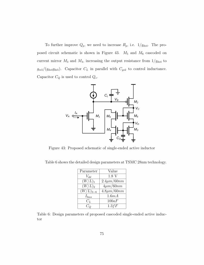
To further improve Qp, we need to increase Rp, i.e. 1/gds4. The pro-
posed circuit schematic is shown in Figure 43. M5 and M6 cascoded on
current mirror M3 and M4, increasing the output resistance from 1/gds4 to
gm5/(gds4gds5). Capacitor CL in parallel with Cgs2 to control inductance.
Capacitor CQ is used to control Qs.
VAIA
M1 M5 M6
M2VB
VC
M3M4
VD
CL
CQ
Figure 43: Proposed schematic of single-ended active inductor
Table 6 shows the detailed design parameters at TSMC 28nm technology.
Parameter ValueVdd 1.8 V
(W/L)1 2.4µm/60nm(W/L)2 4µm/60nm
(W/L)3−6 4.8µm/60nmIbias 1.6mACL 100aFCQ 1.3fF
Table 6: Design parameters of proposed cascoded single-ended active induc-tor
75

Figure 44 shows the simulation result that at 10 GHz, we can obtain a
∼ 600 pH inductor which Q is around 4630.
Figure 44: Simulation result of the proposed single-ended cascoded activeinductor
5.3 Differential Active Inductor
5.3.1 Introduction
Differential active inductor compared with its single counterparts has
two attractive advantages: rejection of common-mode disturbances due to
differential configuration, and double of voltage swing. Conventional differ-
ential active inductor is made up of two differential OTAs or two single-ended
active inductors [59–65]. Figure 45a shows the back-to-back connected dif-
ferential OTA topology and Figure 45b shows the differential OTA composed
76

by two single-ended OTAs.
Vin+
Vin-
C
Cgm1 gm2 I
gm4
gm3C
Vin+ Vin-
C gm1
gm2
(a) (b)
Figure 45: Differential active inductor using differential OTAs
The principle between differential active inductor is the same as single-
ended active inductor addressed previously, where the back-to-back con-
nected OTA+ and OTA- provides 180 phase shift while the parasitic ca-
pacitor offers a -90 phase shift, both together gain a 90 phase shift between
voltage and current and form an active inductor. Some circuit examples are
shown in Figure 46 for the above mentioned topologies.
In Figure 46a, the differential active inductor [60] is constructed by using
two basic differential OTAs. Negative resistors are connected across the OTA
output to cancel out the OTA output parasitic resistances and achieve better
Q. A Q = 600 (at 2GHz) differential inductor is reported in [60] in 0.18um
technology.
Figure 46b shows the differential active inductor based on two single-
ended common-source common-gate (CS-CG) active inductor. The PMOS
common-source stage (M2,M3) is cascoded to have larger output resistance.
77

A cross-couple pair is inserted to cancel out the parasitic output resistance
too. A 70nH Active inductor with Q exceeds 100 is reported [59] from
0.83GHz to 1.33GHz. Various circuits have been proposed to further improve
the active inductor quality factors and tuning range, examples includes using
feedback resistor, etc.
M1 M2
Vb
M5 M6
Vb
-R
-R
M3 M4
M7 M8
Vin+ Vin-Vb1 Vb1Vb2
Vin-Vin+
M1 M2 M3 M4
M5 M6
M7 M8
I1 I2
I3 I4
(a) (b)
Figure 46: Differential active inductor circuit examples
5.3.2 Improved Topology
Compared to single-ended active inductor, differential structure have
inputs(outputs) of opposite phases, this feature enables flexibility of OTA
choices for active inductor, e.g. an active inductor can be composed by two
OTA-. Figure 47 below shows the proposed structure.
78

Vin+ M1 M2
iVin-
i
M3 M4
Ibias1 Ibias1Ibias2 Ibias2
2*Ibias1
VA VB
Figure 47: Schematic of differential active inductor
Its equivalent circuit topology is shown in Figure 48. It is made up of
a differential pair and two single OTA-. Each employed the common-source
single stage amplifier with high input and output impedance. Equivalent
circuit and small signal model are listed in Figure 49 and Figure 50.
in
in
m1
m3
m4
D
C
Figure 48: Circuit topology of differential active inductor
79

Vin+ M1
iVin-
i
M4
Ibias1 Ibias2
VA
Figure 49: Equivalent circuit of differential active inductor
Cgs1
gm1Vin+ gds1 gm4VACgs4 gds4
Vin+ Vin-ii VA
Figure 50: Small signal model of differential active inductor
The input admittance of the active inductor is given by:
Y = s2Cgs2 + 2gds4 +2gm1gm4
sCgs4 + gds1
L =2Cgs4gm1 gm4
Rs =2gds1gm1 gm4
Q =Cgs4gds1
(68)
From Equation 68, Rs is determined by gds1, gm1 and gm4, roughly,
80

gm1 ≈ 10gds1, Rs ≈ 2/10gm4, therefore Rs is limited by the gain of M1 stage
(gm1/gds1) and can not be too small. For a 1nH differential active inductor
we would like to apply in global clock distribution network, Q ≈ ωL/Rs,
with fixed L value, and a relative high Rs, Q can not reach a high value. To
decrease Rs, we need to increase gds1. There are two ways to improve gds1:
to add a cross-coupled pair as a negative resistor to reduce gds1 or to cascode
differential pair to reduce conductance.
5.3.3 Differential Active Inductor with Cross-Coupled Pair Com-
pensation
A Cross-Coupled pair can offer −gm/2 transconductance to reduce Rs
value thus improve quality factor. Figure 51 shows the circuit schematic. And
Figure 52 and Figure 53 are half equivalent circuit model and its correspond-
ing small signal model. Transistor M5 and M6 are cross-coupled pair, which
equals to a negative −2/gm5 shunt resistor to compensate Rs. Transistor
M7 forms a transmission gate and is used to control M5,M6 compensation,
make sure the negative resistor introduced by M5 and M6 does not over-
compensate Rs that leads to oscillation. The resistance of the transmission
gate can be tuned by Vbias.
81

bias
in 1 25 in
3 4
bias1 bias1bias2 bias2
bias1
6
7
A B
Figure 51: Schematic of differential active inductor with CCP
in 1
in
4
bias1 bias2
A
Figure 52: Half circuit equivalent model of differential active inductor withCCP
Cgs1
gm1Vin+ gds1 gm4VACgs4 gds4
Vin+ Vin-ii
-gccp
VA
Figure 53: Small signal model of differential active inductor with CCP
82

The equivalent L and Rs of the differential active inductor with CCP
can be expressed as following, where gtrans is the equivalent resistance of the
transmission gate M7.
L =2Cgs4gm1 gm4
Rs =2(gds1 − gm5) + gtrans
gm1 gm4
Q =Cgs4
(gds1 − gm5) + gtrans/2(69)
By adjusting gtrans with Vbias, Rs can be closed to zero and a large Q is
achieved. To verify the active inductor circuit, a differential active inductor
around 1nH and 10 GHz operating frequency is designed and simulated with
TSMC 28nm technology. The designed active inductor is intended to use as
the active loading of standing wave clock distribution network. The detailed
design parameters are listed in Table 7.
Parameter Value
Vdd 1.8 V
(W/L)1−4 2.4µm/60nm
(W/L)5,6 1.44µm/60nm
Ibias1 940µA
Ibias2 1.655mA
Vcasd 1.58 V
Table 7: Design parameters of differential active inductor with CCP
83

Circuit simulation result is shown in Figure 54. At 10 GHz, inductance
is about 1.2 nH with Q value around 327.
Figure 54: Simulation results of differential active inductor with CCP
Figure 55 shows the tuning range of the proposed differential active
inductor with CCP. The circuit can operated in frequency between 6GHz to
15GHz with Q more than 100.
Figure 55: Tuning range of differential active inductor with CCP
84

Figure 56: THD of differential active inductor with CCP
To verify the voltage swing range that can be applied to the differential
active inductor, total harmonic distortion (THD) is measured on various
input amplitude. The results are shown in Figure 56. The inductor has 1%
THD when input amplitude is 10mV and 10% THD when input amplitude
is about 60mV. Therefore the differential active inductor with CCP is quite
sensitive to its DC operating point and voltage swing, which is also common
for other active inductor designs too [51].
5.3.4 Cascoded Differential Active Inductor
Another method to reduce Rs is cascoding. By cascoding M1 and
M2 with M5 and M6 in differential pair, output conductance is lowered to
gds1gds5/gm5 compared with original gds1. Figure 57 is the circuit schematic
of cascoded differential active inductor.
85

Vbias
Vin+ M1 M2
M5 M6
iVin-
i
M3 M4
Ibias1 Ibias1Ibias2 Ibias2
2*Ibias1
VA VB
VC VD
Figure 57: Schematic model of cascoded differential active inductor
bias
in 1
5
in
4
bias1 bias2
C
A
Figure 58: Equivalent model of cascoded differential active inductor
86

gs1
m1 in
ds1
m4 Cgs4 ds4
in
A
m5 A
ds5
in
C
Figure 59: Small signal model of cascoded differential active inductor
Figure 58 and Figure 59 are the corresponding equivalent circuit model
and small signal analysis. The equivalent L and Rs of the cascoded differen-
tial active inductor can be expressed as following,
L =2Cgs4gm1 gm4
Rs =2(gds1gds5/gm5)
gm1 gm4
Q =Cgs4
gds1gds5/gm5
(70)
It can be seen that Q is improved by gm5/gds5 times. To verify the
active inductor circuit, a differential active inductor around 1nH and 10 GHz
operating frequency is designed and simulated with TSMC 28nm technology.
The designed active inductor is intended to use as the active loading of
standing wave clock distribution network. The detailed design parameters
are listed in Table 8.
87

Parameter Value
Vdd 1.8 V
(W/L)1,2 0.8µm/60nm
(W/L)3,4 0.8µm/30nm
(W/L)5−7 90nm/60nm
Ibias1 700µA
Ibias2 881.6µA
Vbias 1.4 V
Table 8: Design parameters of cascoded differential active inductor for Figure57
Figure 60 shows simulation results of the cascoded differential active
inductor. The inductance is about 1 nH at 10GHz with Q around 344.
Figure 60: Simulation results of cascoded differential active inductor
88

Figure 61 shows tuning range of the cascoded differential active inductor.
The circuit has Q above 10 at frequencye from 8.25GHz to 10.07GHz. The
operating frequency range is roughly 1.8GHz.
Figure 61: Tuning range of cascoded differential active inductor
Total harmonic distortion (THD) is measured on various input ampli-
tude. The results are shown in Figure 62. The inductor has 1% THD when
input amplitude is 25mV and 10% THD when input amplitude is about
450mV. Therefore the voltage swing range of differential cascoded active in-
ductor is larger than the differential active inductor with CCP before.
89

Figure 62: THD of cascoded differential active inductor
90

6 Standing Wave Clock Distribution with Ac-
tive Inductor Loading
6.1 Introduction
In this chapter, active inductors proposed previously is applied to an
X-tree clock distribution network. The design example is intended to deliver
10GHz clock globally with minimum skew and jitter on 28nm technology.
Standing wave clocking with various active inductor loading are compared.
The proposed scheme is compared with implementations in the existing lit-
erature too.
6.2 Standing Wave Clock Distribution with Single-Ended
Active Inductor
VA
IA
M1 M5 M6
M2VB
VC
M3M4
VD
CL
CQ
Active Inductor
Active Inductor
Active Inductor
Active Inductor
Clock
Figure 63: Standing wave on transmission line with active inductor loading
91

Figure 63 shows the circuit schematic of applying proposed single-ended
cascoded active inductor on a transmission line to generate standing wave. To
drive the differential transmission line, two single-ended active inductors are
used to act as a differential active inductor. By applying active inductor on
both sides of the transmission line, the output voltage amplitude is improved.
Figure 64 is the eye diagram and its zoomed in. From Figure 64, clock jitter
is about 189 fs .
(a) Eye-diagram of the circuit
(b) Zoom in of the first eye crossing (c) Zoom in of the second eye crossing
Figure 64: Eye diagram of standing wave on transmission line with activeinductor loading
92

clk
AI
AI
AI
AI
AI
AI
AI
AI
AI
AI
AI
AI
AI
Active inductor
Transmission line
AI
AI
AI AI
AI AI
AI AI AI AI
AI AI
Figure 65: Global clock distribution with active inductor loading circuitschematic
Figure 65 is the circuit schematic of applying proposed active induc-
tor on global clock distribution network. The size of the clock network is
4.96mm× 4.96mm . Parameters are listed in Table 9. Figure 66 is the tran-
sient simulation result. Figure 67 is the eye diagram and its zoomed in. The
reported clock skew is 1.59 ps and clock jitter is about 0.39ps.
93

Item ParametersM1 60nm/2.4µmM2 60nm/9.6µm
M3 ∼ M6 60nm/2.4µmCL 250aFCQ 1.05fFIbias 1.6mAVDD 1.8V
length per segment 1.8mmclock network size 4.96mm× 4.96mm
Table 9: Design parameters of global clock distribution with single-endedcascoded active inductor loading
Figure 66: Transient simulation results for global clock distribution withsingle-ended cascoded active inductor loading
94

(a) Eye diagram of the global clock distribution
(b) Zoom in of the first eye crossing (c) Zoom in of the second eye crossing
Figure 67: Eye diagram of global clock distribution with active inductorloading
95

6.3 Standing Wave Clock Distribution with Differen-
tial Active Inductor(CCP)
Figure 68 shows the schematic of applying differential active inductor
with cross-coupled pair into an X-tree clock distribution network. Figure 69
shows simulation result and Figure 70 shows eye diagram respectively. The
reported clock skew is 0.521ps and clock jitter is about 1ps.
clk
AI
Active inductor
Transmission line
AI
AI
AI
AI
AI
AI
AI
AI AI
AI
AI
AI
Figure 68: Global clock distribution with differential active inductor loadingand cross-coupled pairs
96

Figure 69: Simulation result of global clock distribution with differentialactive inductor loading and CCP
(a) Full eye diagram
(b) Zoom in of the first eye crossing (c) Zoom in of the second eye crossing
Figure 70: Eye diagram of clock distribution with CCP active inductor
97

6.4 Standing Wave Clock Distribution with Cascoded
Differential Active Inductor
clk
AI
Active inductor
Transmission line
AI
AI
AI
AI
AI
AI
AI
AI AI
AI
AI
AI
Figure 71: Global clock distribution with cascoded differential active inductorloading
Figure 71 shows the schematics of applying differential active inductor
with cascoded differential active inductor into an X-tree global clock distri-
bution network. Figure 72 shows simulation result and Figure 73 show eye
diagram respectively. The reported clock skew is about 1.95ps and jitter is
about 0.16ps.
98

Figure 72: Simulation result of global clock distribution with cascoded dif-ferential active inductor
(a) Full eye diagram
(b) Zoom in of the first eye crossing (c) Zoom in of the second eye crossing
Figure 73: Eye diagram of global clock distribution with cascoded differentialactive inductor
99

6.5 Comparison of Various Standing Wave Clock Dis-
tribution
Various clock distribution schemes have been proposed in recent years.
As a comparison, Table 10 summarizes the detailed results from existing lit-
erature and this thesis. It should be noted that most of the results from
literature are based on 180nm and 90nm technology nodes. Since the tech-
nology nodes are evolved in recent year, this thesis uses 28nm process as it
is more likely to be used for digital systems of 10GHz clocks or beyond.
100

Des
ign
Tec
hC
MO
SP
ower
(mW
)F
req(G
Hz)
Jit
ter(
ps)
Ske
w(p
s)T
opol
ogy
Are
a(mm
2)
Sas
aki
[8]
180n
m6A
l80
11.5
4.7
8S
WO
mes
hgr
id5x
5S
asak
i[9
]18
0nm
6Al
819.
55.
20.
8S
WO
rin
gcu
rve
2.2x
2.2
Fra
nk
O’M
ahon
y[4
]18
0nm
6AlC
u46
010
51.
5S
WO
grid
3.6x
3.6
Cod
ero
[5]
90n
m8m
etal
8.2
9.8
3.1
SW
Om
obiu
sri
ng
0.39
x0.
39S
C.C
han
[17]
180n
m6A
l16
81
22L
Cta
nk,
H-t
ree
5x5
Th
isw
ork
180n
m6A
l10
9.8
100.
141.
6S
WO
X-t
ree
7.5x
7.5
Th
isw
ork(s
ingl
e-en
ded
AI)
28n
m11
Al
98.7
910
0.39
1.59
SW
OX
-tre
e4.
96x4.
96T
his
wor
k(D
AI
CC
P)
28n
m11
Al
38.6
710
10.
52S
WO
X-t
ree
4.96
x4.
96T
his
wor
k(c
asco
de
DA
I)28
nm
11A
l55
.49
100.
161.
95S
WO
X-t
ree
4.96
x4.
96
Tab
le10
:C
ompar
ison
ofdiff
eren
tlo
adin
gon
stan
din
gw
ave
clock
dis
trib
uti
onnet
wor
k
101

7 Conclusion and Future Research
7.1 Conclusions
The continuous demand for high-speed high performance microproces-
sors has constantly driven tremendous research efforts for decades. As CMOS
technology scaling from generation to generation, the clock frequency of mi-
croprocessors will be soon approaching and beyond 10 GHz. Recently, there
has been more and more focuses on low power design for better energy con-
served and relaxing the heat dissipation requirement. Majority of modern
digital design are synchronous systems that requires synchronous clocks to
be delivered throughout the entire chip. Traditional clock distribution often
consumes as much as 30%-50% of the total power. Many research efforts
have been spent to explore alternative approaches for better clock skew, jit-
ter control and lower power consumption. Resonant clock distribution is one
of the promising techniques in that it can recycle the energy through the
distributed wire inductance and capacitance.
In this thesis, we try to address some of the topics and open problems
in the standing wave clock distribution, which is one of the resonant clock
distribution schemes. The thesis starts from a literature overview of existing
clock distribution techniques, including traditional clock tree, grid, hybrid
and more recently resonant clock distribution schemes. A brief summary
of transmission line theory is presented to provide enough background for
the discussion later. RLGC model for TSMC 28nm technology is explained.
102

The thesis approaches the practical issues of standing wave clock distribu-
tion by analyzing a 10GHz X-tree global clock distribution design with both
short-end loading and passive spiral inductor loading. One cross-coupled
pairs structure is proposed to compensate the transmission line loss when
it is closed or beyond half of wave length. Detailed simulation results are
presented. The key benefit of using passive spiral inductor loading is that
it can provide almost uniform amplitude output. This greatly relaxes the
buffer requirement as compared to the one in short-end loading scheme.
The thesis extends the idea of passive inductor loading by using active
inductor loading. The key benefit from active inductor loading is its smaller
area overhead, tunability and high quality factor. The design is ready to
be integrated into existed chips as well. Key design issues such as active
inductor designs are explored. Three circuit designs with both single-ended
and differential schemes are proposed. All of them achieves much higher
quality factor than its passive inductor counterpart. The proposed CMOS
active inductors are applied to a X-tree global clock distribution design to
demonstrate the effectiveness of the standing wave generation. Simulation re-
sults show that the proposed clock distribution schemes with active inductor
loading can provide clock delivery with low skew and jitter.
7.2 Future Research Directions
Several practical aspects of this research are worth to check for further
investigation:
103

Firstly, the tuning range of the active inductor needs to be further im-
proved with a reasonable quality factor, e.g. Q more than 10. For modern
microprocessors running at multi-GHz, power saving techniques like Dynamic
voltage and frequency scaling (DVFS) and big-little architecture are vastly
employed. Therefore, the clock frequency spans a huge dynamic range. For
fine-grained power saving, the clock frequency range usually has a variation
of more than 30%. In extreme case that the clock frequency might go down
as far as 10% of its maximum. Mechanisms to switch between standing wave
clock distribution and traditional clock distribution are worth to investigate
too, since it provides a safe alternative and better reliability.
Secondly, the design of effective clock grid for standing wave resonance
is an active research topics as well. Clock networks to completely remove the
requirement of local buffers are actively exploited by various researcher. The
buffer-less clock delivery concept has significant advantage on deep power
saving.
Lastly, a systematic framework including automated clock distribution
design, generation and skew/jitter calculation would be an interesting topic
too. It will make the resonance clock distribution scheme widely deploy and
practically use.
104

References
[1] Naffziger, S.D.; Hammond, G., ”The implementation of the next-
generation 64b Itanium microprocessor,” ISSCC. 2002, pp.344, 2002
[2] Anderson, C.J.; Petrovick, J.; Keaty, etc., ”Physical design of a fourth-
generation POWER GHz microprocessor,” ISSCC. 2001, pp.232, 2001
[3] Chi, V.L., ”Salphasic distribution of clock signals for synchronous sys-
tems,” IEEE Transactions on Computers , pp.597,602, May 1994
[4] O’Mahony, F.; Yue, C.P.; Horowitz, M.A.; Wong, S.S., ”A 10-GHz
global clock distribution using coupled standing-wave oscillators,” IEEE
Journal of Solid-State Circuits, pp.1813,1820, Nov 2003
[5] Cordero, V.H.; Khatri, S.P., ”Clock Distribution Scheme using Coplanar
Transmission Lines,” DATE ’08 Europe, pp.985,990, Mar 2008
[6] Andress, W. F. and D. Ham 2005. ”Standing wave oscillators utilizing
wave-adaptive tapered transmission lines,”IEEE Journal of Solid-State
Circuits, pages 638-651, 2005
[7] Sasaki, M., ”A High-Frequency Clock Distribution Network Using
Inductively Loaded Standing-Wave Oscillators,” Solid-State Circuits,
IEEE Journal of , vol.44, no.10, pp.2800,2807, Oct. 2009
105

[8] Sasaki, M., ”12GHz Low-Area-Overhead Standing-Wave Clock Distri-
bution with Inductively-Loaded and Coupled Technique,” ISSCC. 2007,
pp. 180-595, 2007
[9] Sasaki, M., ”A 9.5 GHz 6ps-Skew space-lling-curve clock distribution
with 1.8 V full-swing standing-wave oscillators,” ISSCC. 2008, pp.
518519., 2008
[10] Wood, John; Edwards, T.C.; Lipa, S., ”Rotary traveling-wave oscillator
arrays: a new clock technology,” IEEE Journal of Solid-State Circuits ,
vol.36, no.11, pp.1654,1665, Nov 2001
[11] V. Honkote and B. Taskin. ”Custom rotary clock router,” International
Conference on Computer Design (ICCD), pages 114-119, October 2008
[12] Honkote, V.; Taskin, B., ”Skew-aware capacitive load balancing for
low-power zero clock skew rotary oscillatory array,” Computer Design
(ICCD), 2010 IEEE International Conference on , pp.209,214, Oct 2010
[13] K. Takinami, R. Strandberg, P. Liang, etc. ”A rotary-traveling-wave-
oscillator-based all-digital PLL with a 32-phase embedded phase-to-
digital converter in 65nm CMOS,” ISSCC 2012, pages 100-102, February
2012.
[14] Z. Yu and X. Liu. ”Implementing multiphase resonant clocking on a
finite-impulse response filter,” IEEE Transactions on Very Large Scale
Integration (VLSI) Systems, pages 1593-1601, November 2009.
106

[15] Drake, A.J.; Nowka, K.J.; Nguyen, T.Y.; Burns, J.L.; Brown, R.B.,
”Resonant clocking using distributed parasitic capacitance,” IEEE Jour-
nal of Solid-State Circuits , vol.39, no.9, pp.1520,1528, Sept. 2004
[16] Chan, S.C.; Shepard, Kenneth L.; Restle, P.J., ”Uniform-phase uniform-
amplitude resonant-load global clock distributions,” IEEE Journal of
Solid-State Circuits, vol.40, no.1, pp.102,109, Jan. 2005
[17] Chan, S.C.; Shepard, Kenneth L.; Restle, P.J., ”1.1 to 1.6GHz dis-
tributed differential oscillator global clock network,” ISSCC. 2005, vol.,
no., pp.518,519 Vol. 1, 10-10 Feb. 2005
[18] Chan, S.C.; Restle, P.J.; etc., ”A Resonant Global Clock Distribution
for the Cell Broadband Engine Processor,” Solid-State Circuits, IEEE
Journal of , vol.44, no.1, pp.64,72, Jan. 2009
[19] Xuchu Hu; Condley, W.; Guthaus, M.R., ”Library-aware resonant clock
synthesis (LARCS),” Design Automation Conference (DAC), 2012 49th
ACM/EDAC/IEEE , vol., no., pp.145,150, 3-7 June
[20] Xuchu Hu; Guthaus, M.R., ”Distributed LC Resonant Clock Grid Syn-
thesis,” Circuits and Systems I: Regular Papers, IEEE Transactions on
, vol.59, no.11, pp.2749,2760, Nov. 2012
[21] Sathe, V.S.; Arekapudi, S.; Ishii, A.; Ouyang, C.; Papaefthymiou,
M.C.; Naffziger, S., ”Resonant-Clock Design for a Power-Efficient, High-
107

Volume x86-64 Microprocessor,” Solid-State Circuits, IEEE Journal of
, vol.48, no.1, pp.140,149, Jan. 2013
[22] Guthaus, M.R.; Venkateswarant, N., etc., ”Gate sizing using incremen-
tal parameterized statistical timing analysis,” Computer-Aided Design,
2005. ICCAD-2005. IEEE/ACM International Conference on , vol., no.,
pp.1029,1036, 6-10 Nov. 2005
[23] A. Rajaram, J. Hu, and R. Mahapatra. ”Reducing clock skew variability
via cross links,” In Design Automation Conference (DAC), pages 1823,
2004.
[24] R.-S. Tsay. ”An exact zero-skew clock routing algorithm,” IEEE Trans-
actions on Computer-Aided Design of Integrated Circuits and Systems,
12(2):242249, 1993.
[25] Kleveland, B.; Lee, T.H.; Wong, S.S., ”50-GHz interconnect design in
standard silicon technology,” Microwave Symposium Digest, 1998 IEEE
MTT-S International , vol.3, no., pp.1913,1916 vol.3, 7-12 June 1998
[26] Anand Rajaram, Jiang Hu, and Rabi Mahapatra. 2004. ”Reducing clock
skew variability via cross links,” DAC ’04, New York, NY, USA, 18-23.
[27] A.Abdelhadi,etal., ”Timingdriven variationaware synthesis of hybrid
mesh/tree clock distribution networks,” Integration, the VLSI journal,
2013
108

[28] Gutnik, V.; Chandrakasan, A.P., ”Active GHz clock network using dis-
tributed PLLs,” Solid-State Circuits, IEEE Journal of , vol.35, no.11,
pp.1553,1560, Nov. 2000
[29] Pratt, G.A.; Nguyen, J., ”Distributed synchronous clocking,” Par-
allel and Distributed Systems, IEEE Transactions on , vol.6, no.3,
pp.314,328, Mar 1995
[30] Saint-Laurent, M.; Swaminathan, M.; Meindl, J.D., ”On the micro-
architectural impact of clock distribution using multiple PLLs,” ICCD
2001 , vol., no., pp.214,220, 2001
[31] Saint-Laurent, M.; Swaminathan, M., ”A multi-PLL clock distribution
architecture for gigascale integration,” VLSI, 2001. Proceedings. IEEE
Computer Society Workshop on , vol., no., pp.30,35, May 2001
[32] Mizuno, H.; Ishibashi, K., ”A noise-immune GHz-clock distribution
scheme using synchronous distributed oscillators,” ISSCC. 1998, vol.,
no., pp.404,405, 5-7 Feb. 1998
[33] Take, Y.; Miura, N.; Ishikuro, H.; Kuroda, T., ”3D clock distribution us-
ing vertically/horizontally-coupled resonators,” ISSCC. 2013, vol., no.,
pp.258,259, 17-21 Feb. 2013
[34] Niitsu, K.; Kulkarni, V.V.; etc., ”A 14-GHz AC-Coupled Clock Distri-
bution Scheme With Phase Averaging Technique Using Single LC-VCO
109

and Distributed Phase Interpolators,” IEEE Transactions on VLSI Sys-
tems, vol.19, no.11, pp.2058,2066, Nov. 2011
[35] Hall, L.; Clements, M.; Wentai Liu; Bilbro, G., ”Clock distribution
using cooperative ring oscillators,” Advanced Research in VLSI, 1997.
Proceedings., Seventeenth Conference on , vol., no., pp.62,75, 15-16 Sep
1997
[36] Galton, I.; Towne, D.A.; Rosenberg, J.J.; Jensen, H.T., ”Clock distribu-
tion using coupled oscillators,” ISCAS ’96., vol.3, no., pp.217,220 vol.3,
12-15 May 1996
[37] Deibele, S.; Beyer, J.B., ”Attenuation compensation in distributed am-
plifier design,” Microwave Theory and Techniques, IEEE Transactions
on , vol.37, no.9, pp.1425,1433, Sep 1989
[38] Restle, P.J.; Jenkins, K.A.; Deutsch, A.; Cook, P.W., ”Measure-
ment and modeling of on-chip transmission line effects in a 400 MHz
microprocessor,”Solid-State Circuits, IEEE Journal of , vol.33, no.4,
pp.662,665, Apr 1998
[39] Restle, P.; C. Carter, etc., ”The clock distribution of the Power4 micro-
processor,” ISSCC 2002, pp. 144145, Feb. 2002.
[40] P. Hofstee, N. Aoki, etc., ”A 1GHz single-issue 64b PowerPC processor,”
ISSCC 2000, pp. 9293, 2000.
110

[41] J. Clabes, J. Friedrich, etc., ”Design and implementation of the
POWER5 microprocessor,” ISSCC 2004, pp. 5657, 2004.
[42] J. Friedrich, B. McCredie, etc., ”Design of the POWER6 microproces-
sor,” ISSCC 2007,pp. 9697, 2007.
[43] N. Bindal, T. Kelly, N. Velastegui, and K. Wong, ”Scalable sub-10ps
skew global clock distribution for a 90nm multi-GHz IA microprocessor,”
ISSCC 2003, pp. 346347, 2003.
[44] S. Tam, J. Leung, etc., ”Clock generation and distribution of a dual-core
Xeon processor with 16MB L3 cache,” ISSCC 2006, pp. 15121521, 2006.
[45] G. Gerosa, S. Curtis, etc. ”A sub-1w to 2w low-power IA processor for
mobile internet devices and ultra-mobile PCs in 45nm Hi-K metal gate
CMOS,” ISSCC 2008, pp. 256257, 2008.
[46] Ackland, B.; Razavi, B.; West, L., ”A comparison of electrical and
optical clock networks in nanometer technologies,” Custom Integrated
Circuits Conference, 2005. Proceedings of the IEEE 2005 , vol., no.,
pp.779,782, 21-21 Sept. 2005
[47] Pham, D.; Asano, S.; Bolliger, M.; etc., ”The design and implementation
of a first-generation CELL processor,” IEEE International Solid-State
Circuits Conference, ISSCC. 2005. pp.184,592 Vol. 1, 10-10 Feb. 2005
[48] TSMC rf0.18 technology manual
111

[49] TSMC 28nm technology manual
[50] Lorentz Solution ®Peakview, Release 3-2-28
[51] Ismail, M, Wassenaar, R. and Morrison, W. ”A high-speed continuous-
time bandpass VHF filter in MOS technology”. Proc. IEEE Int. Symp.
on Circuits and Systems, pp.1761-1764, 1991.
[52] A. Thanachayanont and A. Payne. ”VHF CMOS integrated active in-
ductor,” IEE Electronics Letters, 32(11):9991000, May 1996.
[53] A. Ilker Karsilayan, R. Schaumann. ”A high-frequency high-Q CMOS
active inductor with DC bias control,” Circuits and Systems, 2000. Pro-
ceedings of the 43rd IEEE Midwest Symposium on, 8-11 Aug. 2000
[54] Haiqiao Xiao; R. Schaumann; W. R. Daasch; P. K. Wong; B. Pejcinovic.
”A radio-frequency CMOS active inductor and its application in design-
ing high-Q filters,” 2004 IEEE International Symposium on Circuits and
Systems, Pages: IV - 197-200, 2004
[55] Y. Wu, X. Ding, M. Ismail, and H. Olsson. ”RF band-pass lter design
based on CMOS active inductors,” IEEE Trans. Circuits and Systems
II, 50(12):942949, Dec. 2003.
[56] F. Carreto-Castro, J. Silva-Martinez, and R. Murphy-Arteaga. ”RF low-
noise ampliers in BiCMOS technologies,” IEEE Trans. Circuits and Sys-
tems II, 46(7):974977, Jul.1999.
112

[57] H. Ugur Uyanik, Nil Tarim. ”Compact low voltage high-Q CMOS active
inductor suitable for RF applications,” Analog Integr. Circuits Signal
Process. 51, 3 (June 2007), 191-194.
[58] C. C. Hsiao, ”Improved Quality-Factor of 0.18-m CMOS Active Induc-
tor by a Feedback Resistance Design,” IEEE Microwave and Wireless
Components Letters, vol. 12, no. 12, pp. 467-469, December 2002.
[59] A. Thanachayanont. ”1.5-V high-Q CMOS active inductor for IF/RF
wireless applications,” Proc. IEEE Asia-Pacific Conf. Circuits System,
volume 1, pages 654-657, 2000.
[60] M. Grozing, A. Pascht, and M. Berroth. ”A 2.5 V CMOS differential
active inductor with tunable L and Q for frequencies up to 5 GHz,”
Proc. Intl Microwave Symp., volume 1, pages 575578, Phoenix, May
2001.
[61] F. Mahmoudi and C. Salama. ”8 GHz tunable CMOS quadrature gener-
ator using differential active inductors,” Proc. IEEE Intl Symp. Circuits
Syst., volume 3, pages 21122115, May 2005.
[62] R. Akbari-Dilmaghani, A. Payne, and C. Toumazou. ”A high Q RF
CMOS differential active inductor,” Proc. Intl Conf. Electronics, Cir-
cuits Syst., volume 3, pages 157160, Sept. 1998.
113

[63] L. Lu, H. Hsieh, and Y. Liao. ”A wide tuning-range CMOS VCO with a
differential tunable active inductor,” IEEE Trans. on Microwave Theory
Appl., 54(9):34623468, Sept. 2006.
[64] R. Akbari-Dilmaghani, A. Payne, and C. Toumazou. ”A high Q RF
CMOS differential active inductor,” Proc. Intl Conf. Electronics, Cir-
cuits Syst., volume 3, pages 157160, Sept. 1998.
[65] A. Thanachayanont. ”Low voltage CMOS fully differential active in-
ductor and its application to RF bandpass amplier design,”. Proc. Intl
Symp. VLSI Technology, Systems, and Applications, pages 125128, Apr.
2001.
[66] Chun-Lee Ler, etc. ”Compact, High-Q, and Low-Current Dissipation
CMOS Differential Active Inductor,” IEEE Microwave and Wireless
Components Letters, pages: 683-685, 2008.
[67] Chun-Lee Ler, etc. ”CMOS Active Inductor Linearity Improvement Us-
ing Feed-Forward Current Source Technique,” IEEE Transactions on
Microwave Theory and Techniques, pages: 1915-1924, 2009.
[68] Guthaus, M.R.; Taskin, B., ”High-Performance, Low-Power Resonant
Clocking: Embedded tutorial,” Computer-Aided Design (ICCAD), 2012
IEEE/ACM International Conference on , vol., no., pp.742,745, 5-8 Nov.
2012
114

[69] Frickey, D.A., ”Conversions between S, Z, Y, H, ABCD, and T param-
eters which are valid for complex source and load impedances,” Mi-
crowave Theory and Techniques, IEEE Transactions on , vol.42, no.2,
pp.205,211, Feb. 1994
[70] David M. Pozar, Microwave Engineering, 4th edition, 2012
[71] P. Gray, P. Hurst, S. Lewis, and R. Meyer. Analysis and design of analog
integrated circuits. 4th edition, 2001
[72] Restle, P.; Shan, D.; Hogenmiller, etc., ”5.3 Wide-frequency-range res-
onant clock with on-the-fly mode changing for the POWER8 micropro-
cessor,” ISSCC. 2014, pp.100-101, Feb. 2014
115