CISE 204 DIGITAL SYSTEM DESIGNPage 6 LAB 1: Instruments, circuit board and A simple circuit CISE 204...
44
CISE 204 – DIGITAL SYSTEM DESIGN LABORATORY MANUAL This manual helps to understand basic elements of CISE 204 and its implementation. Dr. Muhammad Faizan Mysorewala Mr. Syed Ameenuddin Hussain Revised in February 2011 by M. Mysorewala 121 King Fahd University Of Petroleum & Minerals
Transcript of CISE 204 DIGITAL SYSTEM DESIGNPage 6 LAB 1: Instruments, circuit board and A simple circuit CISE 204...

CISE 204 – DIGITAL
SYSTEM DESIGN
LABORATORY MANUAL
This manual helps to understand basic elements of CISE 204 and its
implementation.
Dr. Muhammad Faizan Mysorewala
Mr. Syed Ameenuddin Hussain
Revised in February 2011 by M. Mysorewala
121
King Fahd University Of Petroleum & Minerals

Page 2
CISE 204 – Digital System Design 2
TABLE OF CONTENTS
LAB 1: Basic operation of logic gates, instruments and circuit board .......................... 3
LAB 2: TTL Logic & Voltage switching characteristics of basic logic gates ............... 11
LAB 3: Decimal to Binary Encoder ............................................................................... 15
Lab 4: Introduction to Multisim + Example of Molasses Process ............................... 19
LAB 5: BCD to Seven-Segment Decoder ...................................................................... 27
Lab 6: 4-bit Binary Adder/Subtractor and Magnitude Comparator ........................... 31
LAB 7: JK Flop-flop ....................................................................................................... 33
LAB #8: One-shot and Astable Multivibrators for Traffic-signal control system ...... 36
LAB 9: Truncated Sequence using Asynchronous Counter ......................................... 40
LAB 10: Storing to, and Reading from Memory ........................................................... 43

Page 3 LAB 1: Instruments, circuit board and A simple circuit
CISE 204 – Digital System Design 3
LAB 1: INSTRUMENTS, CIRCUIT BOARD AND A
SIMPLE CIRCUIT
Objectives:
The objective of this lab is to learn how to:
Build a simple circuit on the circuit board
Use the instruments such as digital multi-meter (DMM), oscilloscope, power
supply, function generator, etc
Materials Needed:
Power Supply, Function Generator, Oscilloscope, Multimeter, Light-Emitting Diodes
(LEDs), Resistors, Capacitors, and an IC.
(a) Power Supply (b) Function Generator
(c) Oscilloscope (d) Multimeter
Figure L1.1: Instruments

Page 4 LAB 1: Instruments, circuit board and A simple circuit
CISE 204 – Digital System Design 4
Power Supply (Figure L1.1a): All active electronic devices such as the integrated
circuits used in digital electronics require a stable source of DC voltage to function
properly. The power supply provides the proper level of dc voltage. It is very
important that the correct voltage be set before connecting it to the ICs on your
board or permanent damage can result. The power supply at your bench may have
more than one output and normally will have a built in meter to help you set the
voltage. Usually for all circuits power supply should be set to +5.0 V.
Digital Multimeter (Figure L1.1b): the DMM is a multipurpose measuring
instrument that combines in one instrument the characteristics of a dc and ac
voltmeter, a ac and dc ammeter and ohmmeter. The DMM indicates the measured
quantity as a digital number, avoiding the necessity to interpret the scales as was
necessary on older instruments. You need to select the desired function by the
switch provided. For current measurements a separate set of lead connections are
made to the meter. The ohmmeter function of a DMM is used only in circuits that
are not powered.
Function Generator (Figure L1.1c): A function generator is used to produce signals
required for testing various kinds of circuits. For digital circuits, a periodic
rectangular pulse is the basic signal used for testing logic circuits. It is important
that proper voltage be set up before connecting the function generator to the circuit
or else damage may occur. Function generators normally have controls for adjusting
the peak amplitude of a signal and may also have a means of adjusting the 0 volt
level.
Oscilloscope (Figure L1.1d): The oscilloscope is the most important test instrument
for testing circuits and you should become completely familiar with its operations.
It’s a versatile test instrument letting you see a graph of the voltage as a function of
time in a circuit and compare waves. Because an oscilloscope allows you to measure
various parameters, it is considered to be an instrument capable of parametric
measurements important in both digital and analog work. Nearly all complex digital
circuits have specific timing requirement that can be readily measured with a two
channel oscilloscope. There are two basic types of oscilloscope; analog and digital.
Both types of scopes have four main control groups: display controls, vertical and
horizontal control and trigger controls.
Circuit board (protoboards): Circuit boards are convenient way to construct circuit
for testing and experimenting. Most of them look like the one shown in the figure
L1.2 . You will notice the top and bottom horizontal rows are connected as a
continuous row. Vertical groups of five holes are connected together; the vertical
group above the center strip is not connected to vertical group below the center strip.
The holes are 0.1 inch apart, which is the same spacing as the pins on an integrated
circuit DIP (Dual In-line Pins). Integrated circuits (ICs) are inserted to straddle the
center; in this manner, wires can be connected to the pins of the IC by connecting
them to the same vertical group as the desired pin.

Page 5 LAB 1: Instruments, circuit board and A simple circuit
CISE 204 – Digital System Design 5
Figure L1.2: Circuit Board
Exercise 1: Measurement of DC Voltage with the DMM
1. Review the operator's manual or information supplied by your instructor for
the power supply at your lab station. Generally, power supplies have a meter
or meters that enable you to set the output voltage and monitor the current.
Set the voltage based on the power supply meter to +5.0 V and record the
reading in Table 1-1 (in the Data and Observation section).
2. The +5.0 V is the voltage you will use for nearly all of the experiments in this
manual. For most TTL circuits, the power supply should be from 4.75 V to
5.25 V. To check that you have correctly set up the supply, measure the
voltage with the DMM. Record the reading of the DMM in Table 1-1.
Exercise 2: Measurement of DC Voltage with the Oscilloscope
3. In this step, you will confirm the dc voltage from the power supply using the
oscilloscope. Set the SEC/DIV control of your oscilloscope to a convenient
value (a value near 0. 2 ms/div is suggested to give a steady line on the
display). Set the trigger controls to AUTO and INT (internal trigger) to
assure a sweep is on the display. Select channel 1 as the input channel, and
connect a scope probe to the vertical input. Put the input coupling control on
GND to disconnect the input signal and find the ground position on the
oscilloscope (digital scopes may have a marker for the GND level). Adjust the
beam for a sharp, horizontal line across the scope face.
4. Since you will be measuring a positive voltage, position the ground on a
convenient graticule line near the bottom of the display using the vertical
POSITION control. If you are using an analog scope, check that the vertical
VOLTS/DIV variable knobs are in their calibrated positions. A digital scope is
always calibrated, and there is no vernier control.
5. Move the channel I input coupling control from the GND position to the dc
position. For almost all digital work, the input coupling control should be in
the DC position. Clip the ground lead of the scope probe to the ground of the
power supply and touch the probe itself to the power supply output. The line
Page 6 LAB 1: Instruments, circuit board and A simple circuit
CISE 204 – Digital System Design 6
on the face of the oscilloscope should jump up 5 divisions. You can determine
the dc voltage by multiplying the vertical sensitivity (1.0 V/div) by the
number of divisions observed between ground and this line (5 divisions).
Record the measured voltage (to the nearest 0.1 V) in Table 1-1.
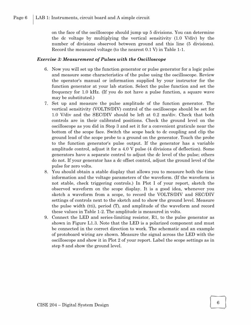
Exercise 3: Measurement of Pulses with the Oscilloscope
6. Now you will set up the function generator or pulse generator for a logic pulse
and measure some characteristics of the pulse using the oscilloscope. Review
the operator's manual or information supplied by your instructor for the
function generator at your lab station. Select the pulse function and set the
frequency for 1.0 kHz. (If you do not have a pulse function, a square wave
may be substituted.)
7. Set up and measure the pulse amplitude of the function generator. The
vertical sensitivity (VOLTS/DIV) control of the oscilloscope should be set for
1.0 V/div and the SEC/DIV should be left at 0.2 ms/div. Check that both
controls are in their calibrated positions. Check the ground level on the
oscilloscope as you did in Step 3 and set it for a convenient graticule near the
bottom of the scope face. Switch the scope back to dc coupling and clip the
ground lead of the scope probe to a ground on the generator. Touch the probe
to the function generator's pulse output. If the generator has a variable
amplitude control, adjust it for a 4.0 V pulse (4 divisions of deflection). Some
generators have a separate control to adjust the dc level of the pulse; others
do not. If your generator has a dc offset control, adjust the ground level of the
pulse for zero volts.
8. You should obtain a stable display that allows you to measure both the time
information and the voltage parameters of the waveform. (If the waveform is
not stable, check triggering controls.) In Plot I of your report, sketch the
observed waveform on the scope display. It is a good idea, whenever you
sketch a waveform from a scope, to record the VOLTS/DIV and SEC/DIV
settings of controls next to the sketch and to show the ground level. Measure
the pulse width (tti), period (T), and amplitude of the waveform and record
these values in Table 1-2. The amplitude is measured in volts.
9. Connect the LED and series-limiting resistor, R1, to the pulse generator as
shown in Figure L1.3. Note that the LED is a polarized component and must
be connected in the correct direction to work. The schematic and an example
of protoboard wiring are shown. Measure the signal across the LED with the
oscilloscope and show it in Plot 2 of your report. Label the scope settings as in
step 8 and show the ground level.

Page 7 LAB 1: Instruments, circuit board and A simple circuit
CISE 204 – Digital System Design 7
Figure L1.3: Example
10. Sometimes it is useful to use an oscilloscope to measure the voltage across an
ungrounded component. The current-limiting resistor, R1, in Figure L1.3 is
an ungrounded component. To measure the voltage across it, connect both
channels of your oscilloscope as shown in Figure L1.4. Make sure that both
channels are calibrated and that the vertical sensitivity (VOLTS/DIV) is 1
V/div for each channel. If you are using a newer scope, the difference
operation (Channel 1-Channel 2) is likely to be shown as a menu item. On
older scopes, the difference measurement is done by inverting channel 2 and
selecting the ADD function. Consult the operator's manual if you are not
sure. Measure the signal across RI and show the result on Plot 3. As a check,
the sum of the voltages across the LED and resistor should be equal to the
voltage of the generator.
Figure L1.4: Oscilloscope for measuring voltage across the resistor

Page 8 LAB 1: Instruments, circuit board and A simple circuit
CISE 204 – Digital System Design 8
Exercise 4: Constructing and Measuring Parameters in a Digital Circuit
11. In this step, you will construct a small digital oscillator. This oscillator
generates pulses that could be used to drive other digital circuits. The basic
integrated circuit for the oscillator is the 555 timer, which will be covered in
detail later. The schematic and sample protoboard wiring is shown in Figure
L1.5. Construct the circuit as shown.
Figure L1.5: Example circuit for rectangular pulse generation
12. Using your oscilloscope, observe the signal on pin 3. Sketch the observed
signal in Plot 4. Be sure to label the plot with the scope settings (VOLTS/DIV
and SEC/DIV). Measure the parameters listed in the first four rows of Table
1-3. The frequency is computed from the period measurement (f = 1/T).
13. Replace Cl with a 100 µF capacitor. The light should blink at a relatively slow
rate. A slow frequency like this is useful for visual tests of a circuit or for
simulating the opening and closing of a manual switch. Measure the period
and frequency of the oscillator with the 100 pF capacitor. This signal, with a
low frequency like this, may give you difficulty if you are using an analog
scope. You will need to use NORMAL triggering instead of auto triggering
and you may need to adjust the trigger LEVEL control to obtain a stable
display. Record your measured values in Table 1-3.
Data and Observations:
Exercise 1 & 2: Measurement of DC Voltage with the DMM and Oscilloscope
Voltage Setting = 5.0 V Voltage Reading
Power supply Meter
DMM (Ex. 1)
Oscilloscope (Ex. 2)
Table 1-1

Page 9 LAB 1: Instruments, circuit board and A simple circuit
CISE 204 – Digital System Design 9
Exercise 3: Measurement of digital parameters
Function Generator
Parameters (at 1 kHz) Measured Values
Pulse width
Period
Amplitude
Table 1-2

Page 10 LAB 1: Instruments, circuit board and A simple circuit
CISE 204 – Digital System Design 10
Exercise 4: Measurement of digital parameters
Table 1-3
Group Members:
(1) ______________________________________
(2) ______________________________________
(3) ______________________________________
(4) ______________________________________
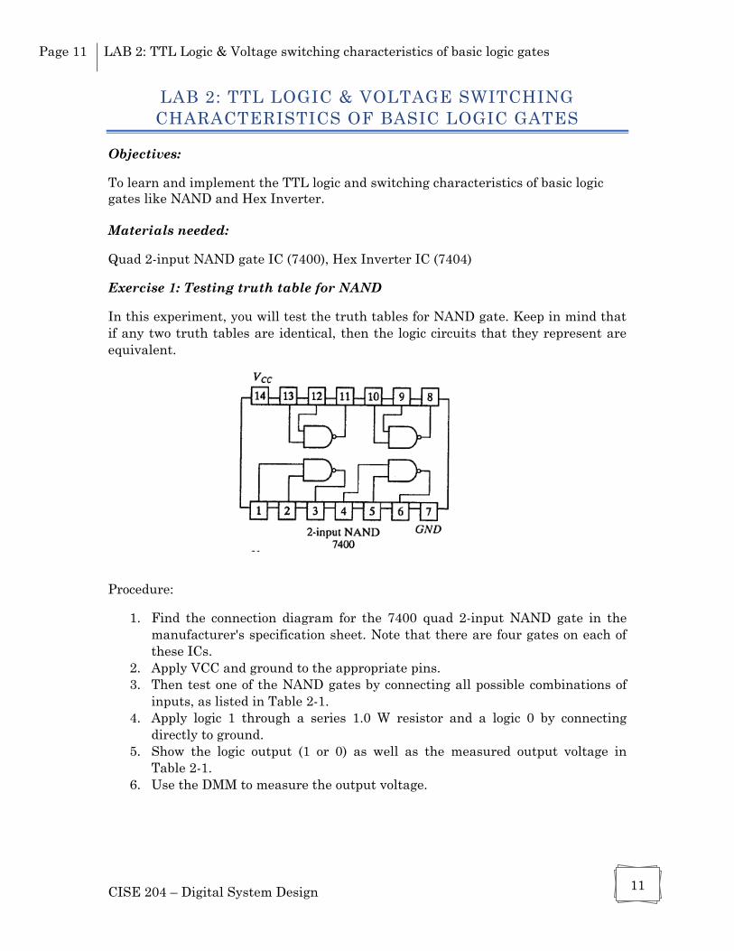
Page 11 LAB 2: TTL Logic & Voltage switching characteristics of basic logic gates
CISE 204 – Digital System Design 11
LAB 2: TTL LOGIC & VOLTAGE SWITCHING
CHARACTERISTICS OF BASIC LOGIC GATES
Objectives:
To learn and implement the TTL logic and switching characteristics of basic logic
gates like NAND and Hex Inverter.
Materials needed:
Quad 2-input NAND gate IC (7400), Hex Inverter IC (7404)
Exercise 1: Testing truth table for NAND
In this experiment, you will test the truth tables for NAND gate. Keep in mind that
if any two truth tables are identical, then the logic circuits that they represent are
equivalent.
Procedure:
1. Find the connection diagram for the 7400 quad 2-input NAND gate in the
manufacturer's specification sheet. Note that there are four gates on each of
these ICs.
2. Apply VCC and ground to the appropriate pins.
3. Then test one of the NAND gates by connecting all possible combinations of
inputs, as listed in Table 2-1.
4. Apply logic 1 through a series 1.0 W resistor and a logic 0 by connecting
directly to ground.
5. Show the logic output (1 or 0) as well as the measured output voltage in
Table 2-1.
6. Use the DMM to measure the output voltage.

Page 12 LAB 2: TTL Logic & Voltage switching characteristics of basic logic gates
CISE 204 – Digital System Design 12
Table 2-1
Exercise 2:
In this experiment, you will test the switching characteristics of the Hex Inverter.
Procedure:
1. Find the connection diagram for the 7404 Hex Inverter in the manufacturer's
specification sheet. Note that there are five inverters on each of these ICs.
2. Apply VCC and ground to the appropriate pins. Then test Hex Inverter gates
by applying the different voltage inputs Vin as highlighted in the Table 2-2.
3. Measure and note the Vout for different values of Vin in Table 2-2. Use the
DMM to measure the output voltage.
4. Start with small step and increase the step size if output voltage is not
changing significantly.
5. Repeat the experiment with different values of VCC = 4.8 V and VCC = 5.2 V.
Figure L2.1: Hex Inverter 7404 and TTL Levels

Page 13 LAB 2: TTL Logic & Voltage switching characteristics of basic logic gates
CISE 204 – Digital System Design 13
Complete the following table for inverter IC 7404.
Vin Vout
Vcc=5.0V Vcc=4.8V Vcc=5.2V
0.1
0.2
.
.
5.5
Table 2-1
Find from the data collected the following for the TTL hex Inverter:
1. Minimum input High voltage (VIH min) : _________________
2. Maximum input Low voltage (VIL max) : _________________
3. Minimum output High voltage (VOH min) : _________________
4. Maximum output Low voltage (VOL max) : _________________
Plot Vin versus Vout for different Vcc values

Page 14 LAB 2: TTL Logic & Voltage switching characteristics of basic logic gates
CISE 204 – Digital System Design 14
Group Members:
(1) ______________________________________
(2) ______________________________________
(3) ______________________________________
(4) ______________________________________

Page 15 LAB 3: Decimal to Binary Encoder
CISE 204 – Digital System Design 15
LAB 3: DECIMAL TO BINARY ENCODER
Objective:
Design, build and evaluate a decimal to binary encoder
Materials Needed:
7432 quadruple 2-input positive-OR gate (Qty=3)
Dipswitch (Qty=1)
330Ω resistors (Qty=3)
LEDs (Qty: 3)
Design of decimal to binary converter
Our objective is to obtain a Boolean function relating the decimal inputs to binary
outputs. We will restrict for simplicity to 7 decimal numbers and 3-bit binary
number.
The decimal numbers range from 0,1,2,3,4,5,6 and 7. Let the decimal number inputs
be denoted as follows
where , , , , , , and
The 3-bit binary outputs be denoted by ,
Boolean expression relating the output, Y, and the input, A is obtained from the
truth table. There are 8 inputs and 3 outputs. At a given instant, only one input, Ai,
may be activated: two or more inputs may not be activated at the same time. To
appreciate this restriction, consider a computer keyboard. One can press only one
number key at any time instant and pressing simultaneously two or more number
keys are not allowed. Truth table for decimal to binary encoder is given in the Table
below. For values of decimal numbers from 0 to 7, corresponding binary numbers are
listed in Table 3-1.

Page 16 LAB 3: Decimal to Binary Encoder
CISE 204 – Digital System Design 16
Table 3-1: The truth table for decimal to binary
Input Output
A0 A1 A2 A3 A4 A5 A6 A7 a2 a1 a0
1 0 0 0 0 0 0 0 0 0 0
0 1 0 0 0 0 0 0 0 0 1
0 0 1 0 0 0 0 0 0 1 0
0 0 0 1 0 0 0 0 0 1 1
0 0 0 0 1 0 0 0 1 0 0
0 0 0 0 0 1 0 0 1 0 1
0 0 0 0 0 0 1 0 1 1 0
0 0 0 0 0 0 0 1 1 1 1
Boolean expression for each of the outputs; , and is obtained by analyzing the
row corresponding to , ,and respectively. From the truth table, it
can be deduced that each binary output is a sum of 4 of the 7 decimal inputs as given
below:
Implementation of the decimal-binary encoder
Each binary output is obtained by using 4 input and one output OR gate. Since OR
gates are available as only two-input and one output gate, three OR gates are
cascade connected.
1A
3A
5A
7A
0a

Page 17 LAB 3: Decimal to Binary Encoder
CISE 204 – Digital System Design 17
A0
A1
A2
A3
A4
A5
A6
A7
a0
a1
a2
Input Decimal
Output Binary
2A
3A
6A
7A
1a
4A
5A
6A
7A
2a
Evaluation and testing of the encoder:
An LED may be connected to each of the outputs. Each of the decimal inputs, Ai ,
where i = 1,2,…7 representing decimal numbers 0,1,..7 is applied by setting the
input to Ai = 5V.
For example when A0 = 5V none of LEDs connected to the binary outputs will light,
when A1 = 5V the LED connected to the binary output a0 will light, when A2 = 5V the
LED connected to the binary output a1 will light, when A3 = 5V the LEDs connected
to the binary outputs a0 and a1 will light, and so on.
Circuit for output :
Input Output Connections for

Page 18 LAB 3: Decimal to Binary Encoder
CISE 204 – Digital System Design 18
Group Members:
(1) ______________________________________
(2) ______________________________________
(3) ______________________________________
(4) ______________________________________

Page 19 Lab 4: Introduction to Multisim + Example of Molasses Process
CISE 204 – Digital System Design 19
LAB 4: INTRODUCTION TO MULTISIM + EXAMPLE OF
MOLASSES PROCESS
Objective:
The objective of this experiment is introducing you to Multisim programming
software with the implementation of simple Molasses Process.
Introduction:
Multisim is the schematic capture and simulation application of National
Instruments Circuit Design Suite, a suite of EDA (Electronic Design Automation)
tools that assists you in carrying out the major steps in the circuit design flow.
Multisim is designed for schematic entry, simulation, and feeding to downstage
steps, such as PCB layout.
Multisim’s user interface consists of the following basic elements:
1
2
3 4 5 6 7 8
9 10
11
12

Page 20 Lab 4: Introduction to Multisim + Example of Molasses Process
CISE 204 – Digital System Design 20
1. Menu Bar
2. Design Toolbox
3. Component Toolbar
4. Standard Toolbar
5. View Toolbar
6. Simulation Toolbar
7. Main Toolbar
8. In Use List
9. Instruments Toolbar
10. Scroll Left/Right
11. Circuit Window
12. Spreadsheet View
The Menu Bar is where you find commands for all functions.
The Design Toolbox lets you navigate through the different types of files in
a project (schematics, PCBs, reports), view a schematic’s hierarchy and show
or hide different layers.
The Component toolbar contains buttons that let you select components
from the Multisim databases for placement in your schematic.
The Standard toolbar contains buttons for commonly-performed functions
such as Save, Print, Cut, and Paste.
The View toolbar contains buttons for modifying the way the screen is
displayed.
The Simulation toolbar contains buttons for starting, stopping, and other
simulation functions.
The Main toolbar contains buttons for common Multisim functions.
The In Use List contains a list of all components used in the design.
The Instruments toolbar contains buttons for each instrument.
The Circuit Window (or workspace) is where you build your circuit
designs.
The Spreadsheet View allows fast advanced viewing and editing of
parameters including component details such as footprints, RefDes,
attributes and design constraints. Users can change parameters for some or
all components in one step and perform a number of other functions.
Problem statement for Molasses Cookie Storage Tank Process Setup:
Control systems typically use sophisticated programmable controllers to provide
flexibility in implementing logic and allowing for changes in the design as
requirements change. For simple systems, the control logic can be designed from
fixed function logic, as will be the case in this experiment. The problem posed in this
experiment is to design the control logic for two of the four outputs in a tank control
system. The specific requirements are described in the Problem Statement. The
problem stated in the experiment is similar, but not identical, to the system
application for the pancake syrup tank explained in Chapter 5. The key difference in
the experiment is that there is feedback present. Strictly speaking this means it is
sequential logic, but the methods employed in the design use combinational logic
design methods (Karnaugh maps) like those discussed in Chapter 5. The feedback
prevents the tank from refilling until it has emptied below a certain level as you will
see. A flow sensor is not needed in this design. The Crumbly Cookie Company has a
problem with the storage tank for its new line of molasses cookies.
The problem is that the molasses in the winter months runs too slow for the batch
process. As a new employee, you have been assigned to design logic for the model-2

Page 21 Lab 4: Introduction to Multisim + Example of Molasses Process
CISE 204 – Digital System Design 21
tank controller that will assure that the molasses is warm enough before the outlet
valve, VouT, is opened. After it is opened, it must remain open until the lower sensor
is uncovered, indicating the tank is empty. The best way to understand the problem
is to review the model - 1 tank controller design. In the model- 1 design, the
molasses tank had two level sensors, one high, LH, and one low, LL. The tank was
emptied (outlet valve opened) only when molasses reached the upper sensor. After
opening, the valve was closed only when the lower sensor was uncovered.
Figure 1: Molasses Process Setup
As mentioned, the model-1 system opens the outlet valve only when both sensors are
covered but, once opened; it remains open until both sensors are uncovered. This
concept requires knowing the current state of the output valve; hence in the design,
it is considered as both an output and an input to the logic. This idea is summarized
with the truth table shown as Table 1. Because the system is designed for TTL logic,
the outlet valve is opened with a LOW signal.
Inputs Output Action
LH LL VOUT VOUT
0 0 0 1 Close valve.
0 0 1 1 Leave valve closed.
0 1 0 0 Valve is open; leave open.
0 1 1 1 Valve is closed; leave closed.
1 0 0 0 Sensor error; open valve.
1 0 1 0 Sensor error; open valve.

Page 22 Lab 4: Introduction to Multisim + Example of Molasses Process
CISE 204 – Digital System Design 22
1 1 0 0 Sensors covered; leave valve open.
1 1 1 0 Sensors covered; open valve.
Table 1 – Truth table Summarized
A Karnaugh map that represents the truth table is shown in
Figure 2. From the map, the minimum logic is determined.
The circuit for the outlet valve of the model-1 tank controller
is shown in Figure 3.
Figure 3: Circuit for output valve of the model-1 tank
Notice that VOUT is returned to one of the inputs, which is the feedback referred to
previously. After constructing the circuit for the outlet valve of the model-1 tank
controller, it will be tested using switches for the inputs and an LED to represent
the outlet valve.
Multisim Tutorial:
This tutorial leads you through the circuit design flow, from schematic capture to
simulation. After following the steps outlined on the following pages, you will have
designed a circuit that you can use to implement the testing procedure without
building a circuit on Multisim.
Schematic Capture:
Opening and saving files
Complete the following step to launch Multisim:
1. Select Start»All Programs»National Instruments»Circuit Design Suite
10.1»Multisim 10.1. A blank file opens on the workspace called Circuit1.
Complete the following steps to save the file with a new name:
1. Select File»Save As to display a standard Windows Save dialog.
2. Navigate to the location where you wish the file to reside, enter MyFirstCircuit
as the filename, and click the Save button.
0 1
00 1 1
01 0 1
10 0 0
11 0 0
Figure 2: K-Map
LHLL
VOUT

Page 23 Lab 4: Introduction to Multisim + Example of Molasses Process
CISE 204 – Digital System Design 23
Tip: To guard against accidental loss of data, set up a timed auto-backup of the file in
the Save tab of the Preferences dialog box.
Complete the following step to open an existing file:
1. Select File»Open, navigate to the location where the file resides, highlight
the file, and click on the Open button.
Tip: To view files from earlier versions of Multisim, select the desired version in the
Files of Type drop-down in the Open dialog.
Components Needed:
One LED
Two single-position DIP switches
Resistors: two 1.0 k4, one 330 S2
IC – 7400,7404 as determined by the student
Placing components:
Complete the following steps to start placing components:
1. Open MyFirstCircuit.ms10 as described above.
2. Select Place»Component to display the Select a Component browser,
search for LED as shown below
and click OK. The component
appears as a “ghost” on the
cursor.
Tip: Once you have selected the desired
Group and Family, start typing the
component’s name in the browser’s
Component field. As you type, the
string appears in the Searching field
at the bottom of the browser. In the
example below, type led. Matches are
displayed as you type.
3. Move the cursor to the bottom-right of the workspace and left-click to place
the component. Note that the Reference Designator for this component is
“LED1.”
4. Place the remaining components in the Digital Counter area as shown below.
Note: When placing resistors, inductors, or capacitors (RLC components), the Select a
Component browser has slightly different fields than for other components. When
placing any of these components, you can choose any combination of: the
component’s value (for example, the resistance value); type (for example, carbon
film); tolerance; footprint and manufacturer. If you are placing a component that
will be ultimately exported to PCB layout, and become part of a Bill of Materials,

Page 24 Lab 4: Introduction to Multisim + Example of Molasses Process
CISE 204 – Digital System Design 24
you must be careful that the combination of values that you select in the Select a
Component dialog box are available in a real-world, purchaseable component.
Tip: When placing RLC components, type the value of the device that you want to
place in the field at the top of the Component list. The value does not need to appear in
the list to be placed on the schematic.
Tip: While placing the 200 Ω resistor, rotate it to a vertical orientation by pressing
Ctrl-R on your keyboard.
Tip: Reference Designators (for example, U1, U2) are assigned in the order the
components are placed. If you place components in a different order than in the
original circuit, the numbering will differ. This will not affect the operation of the
circuit in any way.
Wiring the Circuit:
All components have pins that you use to wire them to other components or
instruments. As soon as your cursor is over a pin, Multisim knows you want to wire
and the pointer changes to a crosshair.
Complete the following steps to wire the circuit:
1. Click on a pin on a component to start the connection (your pointer turns into
a crosshair) and move the mouse. A wire appears, attached to your cursor.
2. Click on a pin on the second component to finish the connection. Multisim
automatically places the wire, which conveniently snaps to an appropriate
configuration, as shown below. This feature saves a great deal of time when
wiring large circuits.

Page 25 Lab 4: Introduction to Multisim + Example of Molasses Process
CISE 204 – Digital System Design 25
3. You can also control the flow of the wire by clicking on points as you move the
mouse. Each click “fixes” the wire to that point. Finish wiring the circuit as
shown below.
Simulation:
Simulating your circuits with Multisim catches errors early in the design flow,
saving time and money. You can simulate the circuit by pressing either “F5”
function button or by navigating to file menu >>Simulate>>Run or by clicking the
green play or run button in the simulation toolbar.
Testing Procedure:
The test begins with both switches closed, meaning the level inputs are both LOW.
As the tank fills, LL is covered, so it will open and changes to a HIGH level. The
LED, representing the valve, remains OFF. Later, LH is covered, so it is opened and
changes to a HIGH level. This causes the LED to turn ON. At this point, closing the
HIGH level switch will have no effect on the LED as it remains ON until LL is again
covered, represented by a LOW.

Page 26 Lab 4: Introduction to Multisim + Example of Molasses Process
CISE 204 – Digital System Design 26
Group Members:
(1) ______________________________________
(2) ______________________________________
(3) ______________________________________
(4) ______________________________________

Page 27 LAB 5: BCD to Seven-Segment Decoder
CISE 204 – Digital System Design 27
LAB 5: BCD TO SEVEN-SEGMENT DECODER
Objective:
Simulate, build and test a simple decoder circuit using a BCD to seven-segment
decoder and a seven-segment display.
Material Needed:
BCD to seven-segment decoder (7447) (Qty=1)
Seven Segment display MAN72A (Qty=1), LEDs (Qty=4)
1kΩ resistor (Qty=1), 330Ω resistors (Qty=11)
Dipswitch (Qty=1)
Theory:
The purpose of BCD-to-seven segment decoder is to decode the input in BCD into 7
output segments for displaying. These decoders are used in conjunction with the
segment displays. There are two main types of decoders as shown in figure below:
- IC 7448, whose inputs and outputs are active HIGH. It is used with MAN74A
(common-cathode type) seven-segment display.
- IC 7447, whose inputs and outputs are active LOW. It is used with MAN72A
(command-anode type) seven-segment display.
MAN74A
MAN72A

Page 28 LAB 5: BCD to Seven-Segment Decoder
CISE 204 – Digital System Design 28
We are using 7447, MAN72A & MAN74. The pin-connections for both are given
below:
Procedure:
First simulate the circuit in Multisim software.
Configure the BCD-to-seven-segment decoder (7447) such that it takes inputs
from four switches and drives the seven-segment display. The 7447 is designed to
properly control a common-anode type of seven-segment display (MAN72).
Provide +5 volt on pin 16 and ground on pin 8 to the 7447 chip.
Apply +5 volt on pins 3, 4, and 5 of the 7447 chip.
Connect 330-ohm resistors to pins 13, 12, 11, 10, 9, 15 and 14 of the 7447, and
connect those resistors to the a, b, c, d, e, f, and g segments of the 7-segment
display.
Connect the common-anode pins 9, 14 of the 7-segment display to Vcc.

Page 29 LAB 5: BCD to Seven-Segment Decoder
CISE 204 – Digital System Design 29
Apply the 4-bit BCD digits through switch and observe the decimal display from 0 to
9. Inputs 1010 through 1111 have no meaning in BCD.
Results:
(1) Show your simulation and the circuit to me, or the lab assistant.
Evaluator’ signatures:______________ (simulation) ________________ (experiment)
(2) Email you simulation file to : [email protected]
(3) Fill the following table using your experimental results.

Page 30 LAB 5: BCD to Seven-Segment Decoder
CISE 204 – Digital System Design 30
Submit this report to me, or the lab assistant.
Group Members:
(5) ______________________________________
(6) ______________________________________
(7) ______________________________________
(8) ______________________________________

Page 31 Lab 6: 4-bit Binary Adder/Subtractor
CISE 204 – Digital System Design 31
LAB 6: 4-BIT BINARY ADDER/SUBTRACTOR
Objectives:
- Build and test the 4-bit binary adder/subtractor circuit.
Material Needed:
7483 (Qty=1), 7404 (Qty=1), 330 ohms resistors (Qty=5), 1 KOhms (Qty=10),
LEDs (Qty=5), Switch (Qty=2)
Theory:
IC type 7483 is a four-bit binary parallel adder. The four bit binary input numbers
are A1 through A4, and B1 through B4. The four-bit sum is obtained from S1
through S4. C0 is the input carry and C4 the output carry.
Two binary numbers can be subtracted by taking the 2’s complement of the
subtrahend and adding it to the minuend. The 2’s complement can be obtained by
taking the 1’s complement and adding 1. To perform A-B, the complement of B is
taken and added to the four bits of A, and 1 is added from the input carry. As shown
in figure below, four XOR gates complement the bits of B when the mode select M=1,
and leaves the bits of B unchanged when M=0. Thus, when the mode select M is
equal to 1, the input carry C0 is equal to 1, and the sum output is A plus the 2’s

Page 32 Lab 6: 4-bit Binary Adder/Subtractor
CISE 204 – Digital System Design 32
complement of B. When M is equal to 0, the input carry is equal to 0 and the sum
generates A+B.
Procedure:
(1) Connect the adder-subtractor circuit by giving input through switches and
outputs connected to LEDs. Complete the table shown below:
Operations
Inputs/Outputs Comment on your result
C0 S C4
9+5
9+15
9-5
5-9
9+9
9-9
Group Members: _______________________________, _____________________________
_______________________________, ______________________________

Page 33 LAB 7: JK Flop-flop
CISE 204 – Digital System Design 33
LAB 7: JK FLOP-FLOP
Objective:
To learn to use flip-flops in digital circuits
Materials needed:
7476A dual JK flip-flop (Qty=1)
390Ω resistors (Qty=3), 1k Ω resistor (Qty=4)
LEDs Red, Green, Yellow (Qty=1 each)
4-position DIP switch (Qty=1)
Theory:
The JK flip-flop is the most versatile of the three basic flip-flops (D, SR). All
applications for flip-flops can be accomplished with either the D or JK flip-flop. The
clocked SR is seldom used; it is used mostly as an internal component of the
integrated circuit.
JK flip-flops are available as either edge or pulse triggered devices. The older 7476 is
a level triggered flip-flop. The 74LS76A is edge-triggered on the HIGH to LOW
transition of the clock.
Procedure:
Build the circuit given below on the circuit board, and take different observations.

Page 34 LAB 7: JK Flop-flop
CISE 204 – Digital System Design 34
Data and Observations:
J K PRE CLR Q Q
0
0
1
1
0
1
1
1
0
1
0
1
1
0
1
1
1
1
1
1
0
1
1
0
1
1
1
1
1
0
0
1

Page 35 LAB 7: JK Flop-flop
CISE 204 – Digital System Design 35
Submit this report to me, or the lab assistant.
Group Members:
(1) ______________________________________
(2) ______________________________________
(3) ______________________________________
(4) ______________________________________

Page 36 LAB #8: One-shot and Astable Multivibrators for Traffic-signal control
system
CISE 204 – Digital System Design 36
LAB #8: ONE-SHOT AND ASTABLE MULTIVIBRATORS
FOR TRAFFIC-SIGNAL CONTROL SYSTEM
Objective:
Learn how to design, simulate, built, and test, one-shot and astable multivibrators,
using the 555 timer.
Materials needed:
555 Timer (Qty=1)
Theory & Procedure:
There are three types of multivibrators: the bistable, the monostable (or one-shot),
and the astable. The name of each type refers to the number of stable states. The
bistable is simply a latch or flip-flop that can be either set of reset and will remain in
either state indefinitely. The one-shot has one stable (or in-active) state and one
active state, which requires an input trigger to assert. When triggered, the one-shot
enters the active state for a precise length of time and returns to the stable state to
await another trigger. Finally, the astable multivibrator has no stable state and
alternates between HIGH and LOW by itself. It frequently functions as a clock
generator, since its output is a constant stream of pulses. Many systems require one-
shot or astable multivibrators.
The traffic signal control system requires two one-shots and an astable multivibrator
as a clock. In this experiment the components for the one-shot and astable
multivibrator is specified, and it is required to test the on-time, frequency and duty-
cycle for the output.
555 is a general purpose IC that can operate as an astable or as a one-shot. As a one-
shot, the timer is limited to pulse widths of not less than about 10µs or frequencies
not greater than 100 kHz. This experiment includes an introduction to the 555
timer, the first and still the most popular timer. It is not a TTL device but can
operate on +5V (and up to +18V) so it can be TTL or CMOS compatible. The timer is
extremely versatile but has limited triggering logic. Some applications include
accurate time-delay generation, pulse generation, missing pulse detectors, and
voltage-controlled oscillators (VCOs).
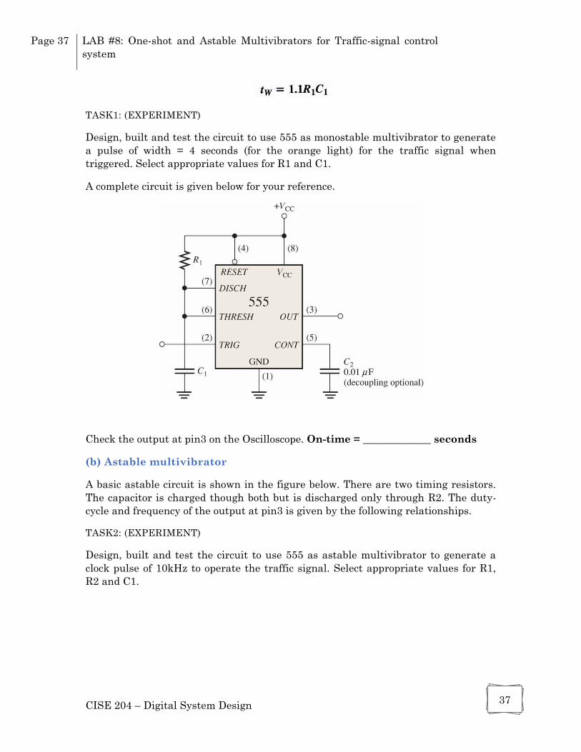
(a) Monostable multivibrator
The following figure below shows the circuit diagram in order to use 555 as a
monostable multivibrator. Assuming LOW state is the stable state of the
multivibrator. Upon giving a HIGH pulse at the TRIG pin (pin 2) for a short interval
of time switches the output pin (pin 3) from LOW to HIGH state. The on-time for the
output pulse is given by:
Page 37 LAB #8: One-shot and Astable Multivibrators for Traffic-signal control
system
CISE 204 – Digital System Design 37
TASK1: (EXPERIMENT)
Design, built and test the circuit to use 555 as monostable multivibrator to generate
a pulse of width = 4 seconds (for the orange light) for the traffic signal when
triggered. Select appropriate values for R1 and C1.
A complete circuit is given below for your reference.
Check the output at pin3 on the Oscilloscope. On-time = _____________ seconds
(b) Astable multivibrator
A basic astable circuit is shown in the figure below. There are two timing resistors.
The capacitor is charged though both but is discharged only through R2. The duty-
cycle and frequency of the output at pin3 is given by the following relationships.
TASK2: (EXPERIMENT)
Design, built and test the circuit to use 555 as astable multivibrator to generate a
clock pulse of 10kHz to operate the traffic signal. Select appropriate values for R1,
R2 and C1.

Page 38 LAB #8: One-shot and Astable Multivibrators for Traffic-signal control
system
CISE 204 – Digital System Design 38
Check the output at pin3 on the Oscilloscope. On-time = _________ seconds, Duty-
cycle = _________ %
TASK 3: (SIMULATION)
Below is the circuit for traffic signal control. Simulate the circuit in Multi-Sim.
- Output 1 generates pulse of width = 25 seconds (Red and Green light) when
triggered. (monostable)
- Output 2 generates pulse of width = 4 seconds (Orange light) when triggered.
(monostable)
- Output 3 generates a clock of 10kHz. (astable)

Page 39 LAB #8: One-shot and Astable Multivibrators for Traffic-signal control
system
CISE 204 – Digital System Design 39
Group Members:
(1) ______________________________________
(2) ______________________________________
(3) ______________________________________
(4) ______________________________________
U1
LM555CM
GND
1
DIS7
OUT 3RST4
VCC
8
THR6
CON5
TRI2
U2
LM555CM
GND
1
DIS7
OUT 3RST4
VCC
8
THR6
CON5
TRI2
U3
LM555CM
GND
1
DIS7
OUT 3RST4
VCC
8
THR6
CON5
TRI2
R12.2kΩ R2
360Ω R31kΩ
R41kΩ
C347nF
C210uF
C110uF
VCC
5V
J1
Key = A
J2
Key = B
X1
2.5 V
X2
2.5 V

Page 40 LAB 9: Truncated Sequence using Asynchronous Counter
CISE 204 – Digital System Design 40
LAB 9: TRUNCATED SEQUENCE USING
ASYNCHRONOUS COUNTER
Objective:
To learn to use counters in digital circuits using the Asynchronous Counter
Materials Needed:
7493A binary Counter (Qty=1)
BCD to seven-segment decoder (7447 or 7448) (Qty=1)
Seven Segment display MAN72A or MAN74A (Qty=1)
1kΩ resistor (Qty=2), 330Ω resistors (Qty=7)
Theory & Procedure:
Digital counters are classified as either synchronous or asynchronous, depending on
how they are clocked. Synchronous counters are made up from a series of flip-flops
that are clocked together. By contrast, asynchronous counters are a series of flip-
flops, each clocked by the previous stage, one after the other. Since all stages of the
counter are not clocked together, a ripple effect propagates as various flip-flops are
clocked. For this reason, asynchronous counters are called ripple counters. Ripple
counter can be made several stages of JK or D flip-flops.
For 7393A, the count advances as the clock input becomes low (on the falling-edge),
this is indicated by the bar over the clock label. This is the usual clock behavior of
ripple counters and it means a counter output can directly drive the clock input of
the next counter in a chain.
The counter is in two sections: clockA-QA and clockB-QB-QC-QD. For normal use
connect QA to clockB to link the two sections, and connect the external clock signal
to clockA. For normal operation at least one reset0 input should be low, making both
high resets the counter to zero (0000, QA-QD low).
Counting to less than the maximum (9 or 15) can be achieved by connecting the
appropriate output(s) to the two reset0 inputs. If only one reset input is required the
two inputs can be connected together. For example: to count 0 to 8 connect QA (1)
and QD (8) to the reset inputs.
Display the outputs QA-QD seven-segment display for counting from 0-9 for 3
different input frequencies (f=0.1,1,10Hz). Use the figure L9.2 given above as
reference.
Connect 1kΩ resistors before Vcc and CLK.
NOTE: Retain your circuit for the next Lab.

Page 41 LAB 9: Truncated Sequence using Asynchronous Counter
CISE 204 – Digital System Design 41
Figure L9.1 (a) Pin connections for 74LS93A, (b) Connections for observations
Data and Observations:
Figure L9.2 Pin-outs for (Left) BCD-to-Seven segment decoder (7447/7448), (Right)
display (MAN72A, MAN74A), (Bottom) HDSP-5501 Common-Anode Seven-segment
Display

Page 42 LAB 9: Truncated Sequence using Asynchronous Counter
CISE 204 – Digital System Design 42
Group Members:
(1) ______________________________________
(2) ______________________________________
(3) ______________________________________
(4) ______________________________________

Page 43 LAB 10: Storing to, and Reading from Memory
CISE 204 – Digital System Design 43
LAB 10: STORING TO, AND READING FROM MEMORY
Objective:
Learn to use memory by building digital circuits using a 16x4 RAM
Materials needed:
74LS189 (16x4) RAM (Qty=1)
4-position DIP switches (Qty=2)
BCD to seven-segment decoder (7447) (Qty=1)
Seven Segment display MAN72A (Qty=1)
1kΩ resistor (Qty=9), 330Ω resistors (Qty=7)
Push button (Qty=1)
Theory and Procedure:
The basic cell in a static RAM is a flip-flop; it can be set or reset for writing
operations or tested without changing its state for read operations. In addition, the
RAM contains logic gates to control the read and write functions and decoding
circuitry. The RAM is organized as an array containing the memory cells in row and
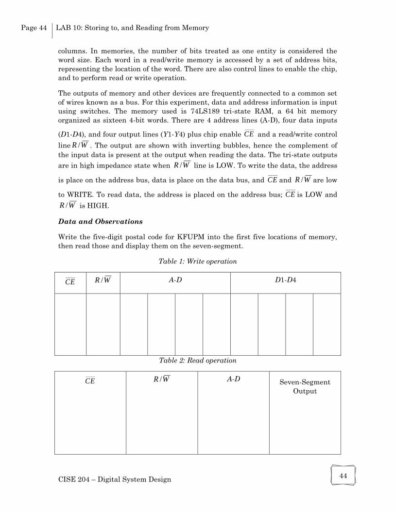
Page 44 LAB 10: Storing to, and Reading from Memory
CISE 204 – Digital System Design 44
columns. In memories, the number of bits treated as one entity is considered the
word size. Each word in a read/write memory is accessed by a set of address bits,
representing the location of the word. There are also control lines to enable the chip,
and to perform read or write operation.
The outputs of memory and other devices are frequently connected to a common set
of wires known as a bus. For this experiment, data and address information is input
using switches. The memory used is 74LS189 tri-state RAM, a 64 bit memory
organized as sixteen 4-bit words. There are 4 address lines (A-D), four data inputs
(D1-D4), and four output lines (Y1-Y4) plus chip enable ____
CE and a read/write control
line WR / . The output are shown with inverting bubbles, hence the complement of
the input data is present at the output when reading the data. The tri-state outputs
are in high impedance state when WR / line is LOW. To write the data, the address
is place on the address bus, data is place on the data bus, and ____
CE and WR / are low
to WRITE. To read data, the address is placed on the address bus; ____
CE is LOW and
WR / is HIGH.
Data and Observations
Write the five-digit postal code for KFUPM into the first five locations of memory,
then read those and display them on the seven-segment.
Table 1: Write operation
____
CE WR / A-D D1-D4
Table 2: Read operation
____
CE
WR /
A-D
Seven-Segment
Output