
Circuit design for energy harvesting from digital TV …1339/...Circuit Design for Energy Harvesting...
91
Northeastern University Thesis by David Lewis 1 Circuit Design for Energy Harvesting From Digital TV Band A Thesis Presented By David Richard Lewis To The Department of Electrical and Computer Engineering In partial fulfillment of the requirements for the degree of Master of Science In Electrical Engineering In the field of Electronic Circuits, Semiconductor Devices, and Microfabrication Northeastern University Boston, Massachusetts July 2012
-
Upload
trannguyet -
Category
Documents
-
view
224 -
download
6
Transcript of Circuit design for energy harvesting from digital TV …1339/...Circuit Design for Energy Harvesting...

Northeastern University Thesis by David Lewis 1
Circuit Design for Energy Harvesting From Digital
TV Band
A Thesis Presented
By
David Richard Lewis
To
The Department of Electrical and Computer Engineering
In partial fulfillment of the requirements for the degree of
Master of Science
In
Electrical Engineering
In the field of
Electronic Circuits, Semiconductor Devices, and Microfabrication
Northeastern University Boston, Massachusetts
July 2012

Northeastern University Thesis by David Lewis 2
Table of Contents:
Chapter 1: Introduction ................................................................................................................... 8
1.1: Solar: .................................................................................................................................... 9
1.2: Vibrational: ........................................................................................................................ 12
1.3: Thermoelectric: .................................................................................................................. 13
1.4: RF Energy: ......................................................................................................................... 15
1.5: Near Field Communication and RFID (NFC): .................................................................. 15
1.6: Applications: ...................................................................................................................... 16
1.6.1: Trickle Charge Battery usage: .................................................................................... 16
1.6.2: Self Powered Applications: ........................................................................................ 17
Chapter 2: RF Energy Harvesting Design .................................................................................... 19
2.1: Villard Voltage Boost Concept: ......................................................................................... 19
2.2: Diode Selection: ................................................................................................................. 20
2.3: Selection of a Low Power Microcontroller (MCU) and Super Capacitor: ........................ 21
2.4: Power Matching Networks: ............................................................................................... 33
2.5: LC Tank Circuit: ................................................................................................................ 35
2.6: Printed Circuit Board Design:............................................................................................ 36
2.7: Simulation Results: ............................................................................................................ 43
Chapter 3: Design Optimization for Ultra Low Power Applications ........................................... 60
3.1: Using a Harvesting Cell Array to Increase Power: ............................................................ 60
3.2: Using a Multiple Band Antenna to Harvest More Energy: ............................................... 63

Northeastern University Thesis by David Lewis 3
Chapter 4: Network Optimization for Ultra Low Power Applications ......................................... 72
4.1: Spread Spectrum Transfer Energy Protocol (SSTEP) ....................................................... 72
4.1.1: Discovery Phase:......................................................................................................... 76
4.1.2: Active Phase: .............................................................................................................. 79
Chapter 5: Integration of the Design Into 45nm CMOS Technology ........................................... 81
Chapter 6: Conclusion and Future Research ................................................................................. 82
6.1: Conclusion ......................................................................................................................... 82
6.2: Future Research ................................................................................................................. 83
6.2.1: Implementation of SSTEP protocol ............................................................................ 83

Northeastern University Thesis by David Lewis 4
List of Figures:
Figure 1: Energy Density of Various Energy Harvesting Sources ................................................. 9
Figure 2: Solar Trash Compactor .................................................................................................. 10
Figure 3: Exponential Relationship of Output Voltage to Input Power ........................................ 19
Figure 4: Harvester and Sensor Block Diagram ........................................................................... 20
Figure 5: Protocol Requirements .................................................................................................. 23
Figure 6: Standard 802.11 DCF Protocol ..................................................................................... 24
Figure 7: Super Capacitor Power Requirements ........................................................................... 24
Figure 8: FET Stage Startup Circuit ............................................................................................. 27
Figure 9: MCU Simulated Charging Region ................................................................................ 28
Figure 10: Micca 2 Charging Regions .......................................................................................... 30
Figure 11: Micca 2 Mote Active Harvesting Region .................................................................... 31
Figure 12: TI Sensor Active Region Wireless -5dBm .................................................................. 32
Figure 13: Micca 2 Mote Power Measurements ........................................................................... 33
Figure 14: S11 Sweep for 10 Stage Harvester .............................................................................. 34
Figure 15: LC Tank Circuit Parameters ........................................................................................ 36
Figure 16: DTV Harvester OrCAD Schematic ............................................................................. 37
Figure 17: Harvester Compared to a Quarter. ............................................................................... 37
Figure 18: Harvester Antenna Compared to Lip Balm Container. ............................................... 38
Figure 19: Chaining Harvesters Together in a Harvesting Array ................................................. 39
Figure 20: PCB Resistance Calculation ........................................................................................ 40
Figure 21: PCB Characteristics ..................................................................................................... 41

Northeastern University Thesis by David Lewis 5
Figure 22: PCB Trace Characteristics Extracted for Simulation .................................................. 42
Figure 23: 10 Stage Schematic With PCB Parasitics .................................................................... 44
Figure 24: 10 Stage Single Array Efficiency ................................................................................ 45
Figure 25: Ideal 7 Stage Single Array Efficiency ......................................................................... 46
Figure 26: 10-Stage 100kohm Load Using Extracted PCB parasitics .......................................... 47
Figure 27: 10-Stage 100kohm Load Using Extracted PCB Parasitics Matched with 1.9pF and
25nH ...................................................................................................................................... 47
Figure 28: Finding Ideal Trace Length for 641Mhz ..................................................................... 48
Figure 29: Frequency Sweep of Unmatched PCB with 250mil Trace Lengths ............................ 49
Figure 30: Comparison Between Simulation and Measured Voltages at Certain Frequencies .... 50
Figure 31: Frequency Sweep of Unmatched PCB Voltage Versus Frequency ............................ 50
Figure 32: Dual Array 10 Stage Harvesters (Efficiency x2)......................................................... 51
Figure 33: Quad Array 10 Stage Harvester (Efficiency x4) ......................................................... 52
Figure 34: Quad Array 7 Stage Harvester..................................................................................... 53
Figure 35: 10 Stage with 6kohm Load Simulating MPPT Regulator ........................................... 54
Figure 36: 10 Stage with 6kOhm Load 4pF and 10nH Match ...................................................... 55
Figure 37: 10 Stage 6kOhm Load with 2pf and100nH Match...................................................... 55
Figure 38: 7 Stage 6kOhm Load With 5nh and 5.5pF Match ....................................................... 56
Figure 39: 7 Stage 6kOhm Load With 2.6pf and 3uH Match ....................................................... 57
Figure 40: 5 Stage 6kOhm Load With 5pF and 0nH Match ......................................................... 57
Figure 41: 2stage 6kOhm Load With 0.6pF and 15nH Match ..................................................... 58
Figure 42: 1 Stage 6kOhm With 50nH and 5pF ........................................................................... 59
Figure 43: Ideal Harvester Array Concept .................................................................................... 61

Northeastern University Thesis by David Lewis 6
Figure 44: Projected Number of Harvesters in Array Versus Power Harvested .......................... 62
Figure 45: Efficiency Versus Number of Harvesters In Array ..................................................... 63
Figure 46: Harvester Open Circuit Voltage Versus Frequency .................................................... 64
Figure 47: Charge Rates from 0v to 1.8v Versus RF Input Power ............................................... 66
Figure 48: Throughput Versus RF Input Power ........................................................................... 67
Figure 49: Antenna Matching Results .......................................................................................... 68
Figure 50: Total System Efficiency .............................................................................................. 69
Figure 51: Charge Rates of Antenna Array Boards from 0 to 1.8v Using 30dbm Output from
Signal Generator and Combined Charge Rate. ..................................................................... 70
Figure 52: Throughput Versus Array Size 641Mhz 0dbm ........................................................... 71
Figure 53: SSTEP Protocol Improving Harvesting Arrays........................................................... 74
Figure 54: SSTEP RF Output Frequency Spread ......................................................................... 76
Figure 55: Voltage Thresholds Used For Node States.................................................................. 79
Figure 56: SSTEP Test Platform................................................................................................... 84
Figure 57: GNURADIO Python Flow Diagram ........................................................................... 85

Northeastern University Thesis by David Lewis 7
Abstract:
Radio Frequency (RF) energy harvesting is relatively unexplored research area, owing to
the challenges involved in converting efficiently the low energy density of RF energy in the ambient
environment to useful electrical power. The proposed research is aimed at making a case for self-
sustaining RF energy harvesting sensors powered by the continuous radiation emitted from
external television (TV) stations as part of their scheduled program broadcasts. This thesis
explores the prototype design and investigates the limitations of creating such a self-powered
network using RF energy harvesting circuits operating around 600 MHz in the VHF digital
television broadcast frequency band. A unique feature of our design is the scalability, wherein
more than one circuit can be joined together to enhance the harvesting capability. Our explorations
in optimizing the energy conversion efficiency of this scalable platform has resulted in
demonstrated improvement by activating multiple frequencies at the same time for transmission,
and using the parallel antenna array that results from the extended circuit platform.
There are three major contributions from our work: The first is analyzing the sensor node
selection (i.e., the choice of the microcontroller) and identifying the best supercapacitor that will
power the sensor for a single packet transmission. The second is designing our harvesting circuit,
fabricating on a PCB, and improving its yield by placing a number of harvesters equipped with
individual antennas in a parallel array. The third topic is demonstrating multiple frequency band
energy harvesting, which accounts for any matching errors in the circuit design that shifts the peak
frequency response of the energy receiver from the idea values. Related to this, we outline an
energy scheduling algorithm called as “Spread Spectrum Transfer Energy Protocol” (SSTEP).
This technique will allow energy transfer from a base station to a set of nodes by building a
frequency spreading table to maximize the efficiency of all or certain nodes.

Northeastern University Thesis by David Lewis 8
Chapter 1: Introduction
Energy harvesting can be divided into several forms of energy sources. Solar,
vibrational, thermoelectric, and radio frequency (RF) energy harvesting are some of the more
popular harvesting techniques. Energy harvesting is extremely important for wireless age to
make devices and networks more portable, longer lasting, and self-sufficient. There are many
wireless energy sources that allow for sensor devices to be sustainable in certain environments.
Most of these sensors are expected to have a wireless sensor network built around them
to minimize the energy consumption of the node, but yet make the data transfer of the node
possible. Networks that provide maximum throughput at lowest network cost are key for this
type of network environment.
Wireless energy for the most part has much less power capability than that of a typical
wire. Below is a table for Energy Harvesting from various sources and the effective energy
available [11][27].
Source Power Notes
Solar 100 mW/cm^2
(directed toward bright
sun)
100 uW/cm^2
(illuminated office)
Most solar cells have very poor efficiency less
than 30%. Best efficiencies today still are below
50%, but theoretical is 80%.

Northeastern University Thesis by David Lewis 9
Vibrational 4 uW/cm^3 (human
motion—Hz)
800 uW/cm^3
(machines—kHz)
Thermoelectric 60 uW/cm^2
RF Energy < 1 uW/cm^2 RF energy can be higher when closer to
transmitter source.
Figure 1: Energy Density of Various Energy Harvesting Sources
1.1: Solar:
Solar cells are very popular today and may be the most commonly used energy harvesting
source. Solar energy harvesting is the most researched harvesting technique today. Solar cells
or photovoltaic cells are solid state p-n junctions that capture incoming photons and convert them
to current. They do this by using band gaps of specific materials at a material junction. Single
material junctions tend to have very low efficiencies of less than 30%. Using multiple material
junctions research has seen around 50% efficiency today. This is still far below the max
theoretical efficiency of 86%[12].
Since the energy density of solar energy is very high around 100 mW/cm^2, solar has a
distinct advantage in energy harvesting. During daylight hours or in an artificially lit
environment solar will provide the most energy for the sensor network it is powering. Solar cells

Northeastern University Thesis by David Lewis 10
are typically made to be stackable in that adding more cells in series and parallel increases the
voltage and current outputs. It does have drawback of being less efficient when not facing direct
sunlight. It also suffers substantially at night when light is minimal.
Solar energy has large corporate support and with government tax breaks for using solar
it clearly is an efficient means of energy harvesting. Companies like Solar City will install solar
panels on a consumer's house for free and collect a monthly payment to allow those who want to
have a green energy source, but cannot afford the upfront installation costs. The company then
takes the solar credits from the government to make up their costs.
Solar trash compactors are placed throughout Northeastern University’s campus. This
shows the many use cases of solar power, the general acceptance in the commercial use cases,
and how enough energy can be harvested over a period of time to run even a garbage compactor.
Figure 2: Solar Trash Compactor
From the higher power harvesting capability solar harvesting is ideal for sensor nodes in
wireless networks as they provide relatively a good amount of power during the day. In [15] a
solar power harvesting solution is presented for Micca 2 sensor motes. The description of the
Northeastern University Thesis by David Lewis 11
maximum power point of the solar power harvesting is a critical point that must be maintained
for maximum efficiency of the solar cell. This concept can be applied to all energy harvesting
techniques where the load strongly affects the efficiency of the harvesting source. The MPPT
regulation algorithm is one of the key finds in the research field for improving efficiency of self-
sufficient solar energy harvesting nodes.
In [22] the MPP tracking algorithm is improved for wireless sensor network nodes by
decreasing the amount of power required to operate the regulator and increasing the durability of
the regulator in different environmental conditions. Up to this point MPPT regulators were
assumed to have plenty of input power to run the regulator. The authors propose a new feedback
approach that consumes less power and is capable of allowing the maximum power point
tracking algorithm to work. For the most part this design is too bulky for a wireless sensor node,
but new regulators like the BQ25504 from Texas Instruments have improved upon this concept
and have led to great improvement in efficiency since the load is essentially disconnected from
the harvesting source. In [23] the authors further enhance the MPPT regulation scheme for solar
powered wireless network nodes, but the consumption is still too high for use in RF energy
applications and is restricted to solar applications.
In [24] an interesting approach was devised where robots are used to provide updates to
the network and transfer energy between nodes to increase efficiency. The network is divided
into energy zones and is updated by energy equalizing technique by moving certain nodes from
energy plentiful areas to energy-starved zones. This is a novel approach to increase overall
network efficiency, but again is limited to solar energy networks due to the energy requirements
of the moving energy equalizers.
Much of the research done in the solar regime can be applied to other types of energy

Northeastern University Thesis by David Lewis 12
harvesting techniques to improve network efficiency.
1.2: Vibrational:
Vibrational energy can be divided into electromagnetic, electrostatic and piezoelectric
energy sources. Typically vibrational energy can gather around 4 uW/cm^3 using human motion
and 800 uW/cm^3 for industrial machinery. The former case allows the most use cases for
commercial applications, but the latter provides much better energy gathering and allows more
useful sensors to be used.
Electromagnetic energy is gathered by magnetic field changes and wire coils. In practice
it can attain 24.8 mJ/cm^3, but can reach 400 mJ/cm^3[27]. This typically is done via magnetics
being moved back and forth by a source of vibration. Several inductive coils are then used to
gather the induced current caused by the magnetic field changes. A famous use case of this is the
―shaker flashlight‖ where a magnet is placed in a flashlight tube. As you shake the flashlight the
magnet is moved back and forth inside a coil of wire. The wire induces an electrical current and
then the voltage is rectified for use by the light bulb.
Electrostatic energy can also be created by using changes in plate capacitance of loose
plates in a capacitor. In practice it can attain 4 mJ/cm^2, but can reach 44 mJ/cm^3[27]. The
electrostatic energy is gathered using changes in capacitance between vibrational dependant
varactors by using the distance of the parallel plates to change the capacitance. Since
capacitance is directly proportional to distance the vibration allows a somewhat linear change in
capacitance, which can be used to generate a charge. In [30] this is implemented and simulated
to have variable capacitor with the range of 1-100pF subject to vibrational energy every 15us
will produce about 38 uW of power. The author uses a three-phase system that separated into

Northeastern University Thesis by David Lewis 13
pre-charge, harvest, and recovery phases. The system in package used requires the fabrication of
a MEMS variable capacitor as the critical feature. Unfortunately this system requires a low
power DSP to cover the power management features and also requires the vibrational energy to
be synchronous like that of a engine. This approach is not adaptable to human vibrations.
Piezoelectric energy converts mechanical strain energy into electrical charge. It can in practice
attain 35.4 mJ/cm^3, but can reach 335 mJ/cm^3[27]. As piezoelectric materials contract and
expand they create a charge similar to that of the electrostatic case. Since mechanical strain by
nature is capacitive it can be used in this manner to gather energy. Most cantilever piezoelectric
devices fabricated today can obtain high energy densities, but only at a specific resonant
frequency.
Piezoelectric energy requires optimizations to gather the maximum amount of energy
possible. In [28] the maximum efficiency duty cycle was found for piezoelectric sources using a
discontinuous conduction type regulator. This type of regulation technique can improve the
power harvested by certain sources up to 325%. In [29] a full wave rectifier is fabricated on chip
and allows efficiency up to 93% for the piezoelectric transducer used. The transducer used also
is an improvement from the cantilever approach as it improves the frequency range of use by
allowing multiple resonances. This allows its use to be broader since random vibrational sources
can be used.
1.3: Thermoelectric:
Thermoelectric is another form of energy harvesting used today. With 60 uW/cm^2 it
has more energy harvesting capability than that of typical vibrational and RF energy sources.
Thermoelectric energy harvesting works by using temperature gradients on a conducting material

Northeastern University Thesis by David Lewis 14
produce a voltage. This is due to the diffusion of charge carriers based on the temperature
difference. Thomas Seebeck discovered this effect in 1821. Charles Peltier improved upon this
concept when he discovered that a metal junction of two dissimilar conductors could produce a
current.
The best materials to use for thermoelectric energy harvesting sources are highly
conductive metals with low thermal conductivity. The low thermal conductivity allows the
thermal gradient between different points on the metal to be maintained. The high conductivity
allows for more diffusion of carriers and also less loss in the transfer of energy from the source
to the system.
Some of the more common uses for these materials are for thermocouples, which are
used to measure temperature. They do so by converting the temperature measured to a voltage
that a multimeter could convert to temperature.
In [25] the authors show a SOC approach to combining thermoelectric and RF energy
sources together to provide power to a micro battery. This approach of combining two smaller
sources together has a big advantage when one of the sources is non-existent in a particular
environment. This concept of combining energy harvesting sources is not new, but optimizing
some networks with environment susceptibilities is a good optimization to allow more network
robustness.
Thermoelectric energy has many application cases in the biomedical field since the
human body is a good source of heat. In [26] a bismuth and antimony p-n junction was formed
to harness thermal energy from the human body. The fabrication process reveals that these
junctions are somewhat easy to create in current solid-state fabrication technologies. The
experimental results show as high as 10v can be created using the human forehead. This paves

Northeastern University Thesis by David Lewis 15
the way for self-sufficient biomedical sensors for patient recovery and monitoring.
1.4: RF Energy:
RF energy can be broken up into smaller sub-topics based on the method the power is
received. RFID and NFC are a similar topic since NFC is an improvement upon the former
RFID standard. In all cases RF energy transfer is very small compared to solar energy. RFID
and NFC for instance rely on the power transmitter to be very close to the harvesting device.
Charging pads like that of the Powermat [14] use very near field inductive coupling to
create a transformer to transfer energy. This is not as much RF as it is a creation of a transformer
with two inductive coils. When a current pushed through the charge pad’s coil a current is
induced on the devices charge case. This is then regulated for the particular voltage that the
device may take. This is typically 5v.
1.5: Near Field Communication and RFID (NFC):
RF energy harvesting becomes more and more popular as NFC applications take hold in
today’s markets. NFC is an improvement on RFID by adding two-way communication. Prior to
this RFID was a one-way communication by the reader. It uses 13.56Mhz as its frequency band
of operation and uses inductive coupling of each devices loop antenna to harvest its power. It is
limited to about 4 centimeters in range and only about 424 kbits/s bit rate.
Most cell phones on the market already have NFC support. Major manufacturers have
been constantly adding NFC as a required feature in their RFQ’s for future product development.
This is driven by the great potential that NFC has of replacing our current monetary system.
Google wallet leads the way in this field and combined with Paypass has a small backbone in

Northeastern University Thesis by David Lewis 16
place already. In the same way that RFID works NFC gathers energy from a transmitter for long
enough to send a data packet that contains its RFID tag. This tag can then be processed by a
network based application to determine what this product or device is. In a simple example a
cell phone is equipped with a NFC reader, which acts as a power transmitter to a device. The
device could be any product in a grocery store for instance. The product must have a NFC
device embedded in the packaging of the product. When the cell phone is brought close to this,
or ―tapped‖ to the product the item’s RFID string is read by the phone. The phone running a
NFC enabled network application then looks up the product id and brings up a picture of the
product on your phone and gives an option to view the price and or just purchase the product.
As one could see this simplifies the consumers experience at the store considerably. It
also allows marketing of the product to directly interact with the consumer at the time of
purchase. If the consumer looks at the product the network application could bring up an
Internet ad for the product and product comparisons with leading competitors. Other external
sources could also be added including coupons for that particular product or sales prices of the
exact same product a competing store.
1.6: Applications:
There are limited applications where such low energy content is capable of being used.
The following are several types of application scenarios that give a good fit for this type of
harvesting.
1.6.1: Trickle Charge Battery usage:
A clear scenario would be using this harvesting mechanism to trickle charge a sensor

Northeastern University Thesis by David Lewis 17
node with an existing battery. This would extend the life of the battery and even fully charge the
battery when the sensor is consuming less power than it is receiving. This would typically be in
a sleep state where the consumption of the MCU is minimal and the RF input energy is high
enough to provide enough charge for the battery.
1.6.2: Self Powered Applications:
Self-powered applications are more limited due to the low energy densities of ambient
RF energy. The expected application would hence need to employ a base station that transmits
enough RF power to charge the sensors in range of it. This would imply a one-way network
where the base station is constantly collecting data from sensor nodes only when the sensor
nodes have gathered enough power to transmit. This is not a difficult scenario to manage.
Commercial applications of this already exist created by a company called PowerCast. Their
short-range RF energy sensors require a base station that is constantly transmitting power at
928Mhz. This allows sensors to either be self-powered using a super capacitor as an energy
storage device or a battery. The sensors in the network are capable of short transmission bursts
and then returning to sleep until enough energy is harvested again.
This type of application is best realized in a fixed environment such as an industrial
facility, an office environment, or a home automation environment. The major requirement in
this type of network is the range of the transmitter in the building selected and the sensor node
placement as to maintain enough input power to charge the node.
Home automation is a growing market today and offers a lot of potential for RF energy
harvesting. A possible application case for the home automation is using a central base station in
ones home like an existing Wifi router for an energy harvesting source and a separate base

Northeastern University Thesis by David Lewis 18
station, possibly integrated with the Wifi router to conduct packet transactions. The energy
wasted by constant transmission of Wifi routers could be used to slowly charge sensor nodes
throughout a person’s house. The advantage to this system is that the power source already
exists in a lot of US homes today. The main drawback to this approach is the relatively low
output power from Wifi routers and the attenuation of 2.4Ghz in air. Although 4-Watt
transmission is possible typical Wifi routers are only around 200 mW of output power.
This market has already been taken over by many wireless protocol networks including
Zigbee, 6LoPAN and Wifi. Wifi has the upper hand as far as acceptance with the general
market, but Zigbee and other low power protocols tend to have an advantage with devices that
are battery operated including smoke detectors, thermostats, and carbon monoxide detectors.
Using optimization design technique such as multiple arrays, multi-band antennas, and SSTEP
protocol proposed in this thesis, RF harvesters could find their way into devices where very little
power is used the majority of the time and only short bursts are required to gather the
information like temperature in many rooms of a house.
Northeastern University Thesis by David Lewis 19
Chapter 2: RF Energy Harvesting Design
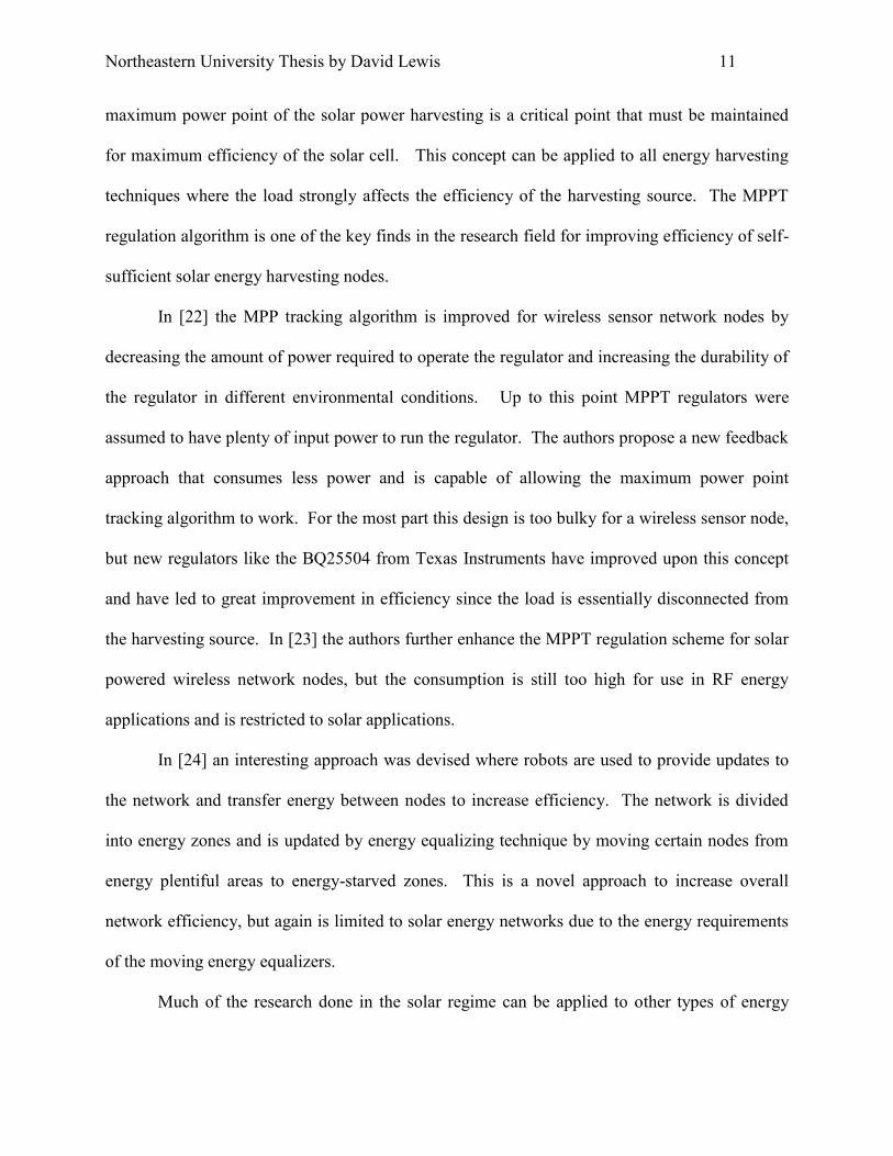
2.1: Villard Voltage Boost Concept:
The proposed method of harvesting RF energy is a variant of the design proposed in
[need citation for our first paper]. The design is built on a power over air harvesting concept
proposed by Telsa in 1904 [6]. The proposed circuit design utilizes a Villard cascade voltage
multiplier circuit was invented by Heinrich Greinacher in 1919[need citation]. The multiplier
acts as a charge pump to effectively both rectify and multiply the input voltage. The circuit used
is a half wave version of the circuit and depends heavily upon impedance matching for
maximum power transfer. The design hence is a non-linear system where input voltage and
number of stages have an exponential relationship with output power.
Figure 3: Exponential Relationship of Output Voltage to Input Power

Northeastern University Thesis by David Lewis 20
Using the voltage multiplier as a way to rectify small RF input amplitudes gives way to a
circuit design concept below.
Figure 4: Harvester and Sensor Block Diagram
2.2: Diode Selection:
The voltage multiplier works best when the barrier height of the Schottky diodes used are
as low as possible. The HSMS-2852 series diodes are some of the lowest barrier diodes that are
available to purchase with an easy to use surface mount package. The RF diodes surveyed for
construction of this multiplier tend to fall into RF detector application category. Although this
category has similar characteristic requirements, the diodes in these applications tend to not have
a metric for barrier height in their datasheets. The metric used to determine the best diode choice
is the turn on voltage level, which is extrapolated from the given input voltage versus output
curve. The HSMS-2852 series offers the lowest available turn on voltage in a surface mount
package.
Another key metric of the diode is the internal resistance. To minimize power loss this
resistance must be kept to a minimum. Parasitic inductances as well must be kept to a minimum
so packaging choices are key to keep losses in check.

Northeastern University Thesis by David Lewis 21
2.3: Selection of a Low Power Microcontroller (MCU) and Super Capacitor:
In [13] it was found that using super capacitors allow for much longer lifetimes than that
of batteries since they offer much higher charge cycle counts over the lifespan. The requirement
then became using the Maximum Power Point Tracking (MPPT) of the solar cell to operate the
voltage reference of a PFM mode buck regulator. This relates strongly to all energy-harvesting
designs and is a requirement to have a PFM mode regulator with MPPT algorithm support. For
this reason a Texas Instruments BQ25504 is used after the harvester stage to charge a super
capacitor for the sensor MCU. Unfortunately there are no MPPT regulators catering to the high
impedance required to operate the energy harvesting circuit so even with this MPPT regulator the
circuit requires to be pre-charged to at least 2.5v to start reliable operation. This problem should
be focused on in future work.
The maximum power point can be found for the RF energy harvester as well by finding
the maximum open circuit output voltage. This point should then be used to feed the reference
of the PFM regulator for the MCU voltage. By using a PFM mode regulator with MPPT support
we are able to sample the open circuit input voltage and adjust the switching of the regulator to
maximize this operating point. This in effect raises the output impedance seen by the harvester
circuit, which would otherwise see close to a dead short from the super capacitor. By allowing
this operation the efficiency of the harvester can somewhat be maintained even with changing
the output loading substantially. This is a must have for charging from a dead node, but also
useful in total efficiency in the active region of operation.
In calculating the worst-case power the sensor node can consume we must first
understand what protocol it uses and how much power it takes to transmit a packet. If we take
the assumptions that the sensor node is following an 802.11 protocol then we can define the

Northeastern University Thesis by David Lewis 22
expected transmission time and with a power measurement during constant transmission we can
calculate the joules of energy required to be generated by the harvester during a single packet
transmission. The following table shows the key parameters for the protocol and the time that
each portion of the protocol takes. This assumes that if a packet is lost the transmitter will not
care. Its data is retransmitted from the beginning each time and therefore packet loss is not
calculated here. We do not calculate the throughput of the system here, but rather only the
power required per packet of transmission.
For this particular system we assume that a node is really a data gatherer and mostly
transmitting data to a fixed node. Therefore there is an assumed receiver that is always active in
the system. It is also assumed that the receive time is the same as the transmit time. To receive
data the receiver would have to look for a packet addressed to it at the time of wake up. If this
packet does not occur and the channel is free it is assumed that the node will transmit its gathered
data to the always active receiver and go back to sleep.
The worst-case power consumption during a single packet is when the maximum back off
time and maximum packet size are used simultaneously. In this particular scenario we can
determine the worst-case power consumption of the MCU and from that calculate the minimum
required capacitor for charge storage. The capacitor must be sized as small as possible for the
harvester to maximize its charge time. The harvester also has a minimum required received
power that is variable based on the capacitor used and the MCU load on the rail. For this reason
minimizing the capacitor to the protocol requirements is the best way to ensure that reasonable
charge times and minimum receiver power are used. Below is a table showing a use case for the
requirements of the capacitor.
Protocol Time Requirements

Northeastern University Thesis by David Lewis 23
DIFS 50 Us
SIFS 10 Us
Slot Time 20 Us
Number of Slots 64
BPS 192000 b/s
Max Packet Size 512 bytes
Size of Data 21333.33333 us
RTS 666.6666667
CTS 666.6666667
ACK 666.6666667 us
Propagation Delay Round Trip 20m 0.066666667 us
Max Packet TX Time 24673.4 us
Required Seconds 0.0246734
Power Margin 20 %
Required Joules 0.001110303 J
Required Capacitance 0.004996364 F
Figure 5: Protocol Requirements

Northeastern University Thesis by David Lewis 24
These protocol timing requirements assume the standard DCF protocol seen below:
Figure 6: Standard 802.11 DCF Protocol
Capacitor Choice
V (Volts) 3 3 3 3 3
C (Farads) 0.000047 0.1 0.02 0.22 0.22
Energy (Joules) 0.0002115 0.45 0.09 0.99 0.99
Power Per 5 Seconds (W) 0.0000423 0.09 0.018 0.198 0.198
Power Per 30 Seconds (W) 0.00000705 0.015 0.003 0.033 0.033
Power Per Minute (W) 0.000003525 0.0075 0.0015 0.0165 0.0165
Power Micca 2 (W) 0.045
Figure 7: Super Capacitor Power Requirements

Northeastern University Thesis by David Lewis 25
One problem with the charging circuit is that when the voltage threshold is reached for
the MCU it will turn on and cause inrush current and droop the voltage back out of the operating
region. Since the harvester can only overcome the discharge rate of the MCU when it is in sleep
mode and not in active transmission or at POR time it is important to overcome this start up
problem. If this is not addressed the charger will ramp the voltage until the MCU becomes
active. Then the MCU will drop the voltage back out of the active region and the this process
will repeat with the MCU never seeing enough voltage for a long enough period of time to
process anything.
One way to overcome this problem is to implement a power on latch the keeps the MCU
in reset while the charging circuit surpasses the turn on threshold and continues to a targeted set
point. The set point is best to be set at the maximum allowed recommended voltage to power the
MCU. In a lot of cases this is the nominal voltage VDD plus 5%. The power on latch circuit
desired uses a d-flop to create this effect. The clock input is positive edge triggered and the flop
is chosen based on minimum power consumption. Since most MCU resets are active low one
should use a non-inverting d-flop. The clock input should have a hysteretic type input to get a
clean positive edge. Note that this approach depends on having an MCU that either does not
have a built in power on reset circuit or if it does that it is open drain style drive such that there is
no contention on the reset line.
Using a 74LVX series part is a good choice for most low power MCU’s. This part allows
working at 2.0v to 3.6v, which covers most of the low power MCU market. The part also
maintains its state down to 1.2v such that the MCU can use as much of the capacitor energy as
possible during discharge. In the figure below the charge ramp of the capacitor is shown during
charge and discharge phases. The power latch circuit allows the capacitor to charge to 3.15v and

Northeastern University Thesis by David Lewis 26
then toggles reset from low to high. When this occurs the MCU wakes up for a brief period of
time and transmits. This is called the discharge time. It is a much steeper discharge rate than
that of the charge rate.
Depending on the MCU used the active region changes. In this example it is only from
the 3.15v to 2.1v. During this time the MCU must wake up and either transmit its data or receive
from the base station. It can either go back to sleep on its own, which will allow a faster charge
time or run until power is low enough for the flop to reset the MCU. If it chooses to sleep on its
own it must remain in sleep for the full charge rate time to get back to 3.15v. To do this it must
either periodically monitor the voltage with an ADC, or it must wait for a known amount of time
that would guarantee a full charge. One could assume 5*RC to get to the full charge time. The
other unknown is in this approach is the RF signal power is assumed to be constant to know the
RC time constant. If the signal power drops during this period then the sensor will not be fully
charged when it wakes up and most likely will dip below the non-active voltage boundary and
the flop will then reset the device and begin a charge cycle.
A latch to hold reset state is a valid approach but does not prevent leakage current flow
from the MCU during power down. The best approach has been found to be that when a voltage
is less than the lower threshold the MCU should be turned completely off to maximize the charge
rate of the super capacitor. This can be done using a two-stage FET configuration that utilizes
the voltage thresholds of the transistors to connect VDD to the MCU. The voltage threshold of
the PFET must be chosen in a way to turn on around -2.5v and the NFET threshold voltage must
be chosen to be around 55% of the VDD used for the MCU. In this case the MCU VDD is 3.3v
so we choose a 1.8v threshold. As the voltage is applied from the harvester the output to the
MCU is nothing. When the harvester input is 2.5v the voltage at the gate of the NFET becomes

Northeastern University Thesis by David Lewis 27
1.25v. From here as the voltage increases from the harvester the half of that voltage is applied to
the gate of the NFET. When 1.8v is reached at the gate of the NFET we have approximately
have 3.3v applied to the MCU.
Figure 8: FET Stage Startup Circuit
The proposed MCU charging algorithm requires two threshold levels. One is the
transmission threshold and one is the must sleep threshold. The transmission threshold is best set
at the upper limit of the recommended operating conditions of the MCU. The must sleep
threshold should be set at the lowest recommended operating voltage. As an example for a 3.0v
MCU this would be 3.15v for the transmission level and 2.85v for the must sleep level.
With the power trip switch in place when the lower threshold voltage is reached the MCU
will turn on. At this point in time the MCU should sample the voltage with its ADC and then go
into a low power sleep mode. Using an internal timer the MCU waits 5 seconds and wakes up to
then again sample the VDD voltage. The cycle repeats until the transmit threshold voltage is

Northeastern University Thesis by David Lewis 28
reached. In this case it waits until 3.15v is sampled by the ADC. When the upper transmission
level is reached the sensor will transmit its data to the base station.
Below is a simple simulation with the expected behavior during the active region. We confirmed
this theoretical behavior with the Micca 2 mote.
Figure 9: MCU Simulated Charging Region
We programmed both a Micca 2 sensor and a Texas Instruments MSP430 on the eZ430-
RF2500-SEH platform to follow this algorithm. Since the ADC uses an internal band gap
voltage as its reference VDD can be measured without the effect of changes in VDD changing
the ADC codes expected. If this was not the case an external reference must be used for the
ADC. Either using a Zener diode or some other band gap reference. The power on switch
threshold must be higher than that of the ADC band gap reference or else the MCU will turn on

Northeastern University Thesis by David Lewis 29
and start sampling before the band gap has been reached. In this scenario the design would not
be able to charge effectively.
The below experiment is the voltage output of the Micca 2 sensor over time without a
power latch using a 100mF super capacitor and a single harvester circuit. An RF signal
generator for precision controls the RF input power. The input frequency used was 641Mhz.
The input power was varied during the charge ramp to see the minimum RF input power levels
required to charge from a dead node as well as to maintain an active state.
All MCU’s have an initial current spike in consumption based on transistor turn on
thresholds. Most MCU’s have a specific minimum power on ramp rate to avoid latch up
conditions. Because the charge rate of the harvester is very slow we run into conditions that
faster charge rate input voltage ramp would not see. Through some experimentation it was found
that 1.2v is a critical region of the Micca 2 sensor and hence needs to be avoided. Our power
latch circuit prevents the MCU from being powered during this period and allows us to use a
much smaller input power to complete charge from dead start.
Without the power latch the MCU required 10dbm RF input power at 641Mhz to
overcome the behavior of the Micca 2 sensor with a slow charge ramp. Once the active region
was reached the RF power to maintain the active region was explored. To maintain charge at the
minimum threshold -10dbm was required. Charging occurs with any input power more than this,
but lower input power takes more time between transmissions.
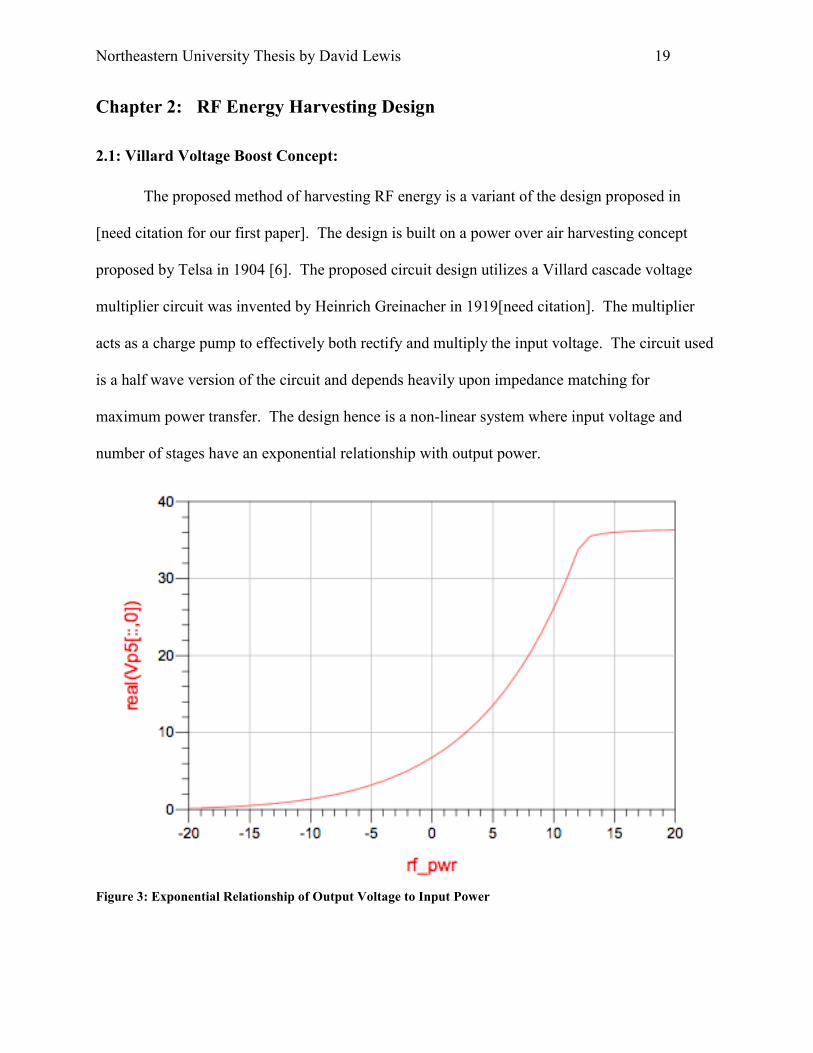
Below is the logged Micca 2 VDD voltage output from the harvester during the
experiment. The time step is in 500ms intervals. In the first 335 time steps only 0dbm was
applied to the circuit. At 335 to 1003 steps 5dbm was applied to the circuit. At 1003 to 2673
7dbm was applied. After this gets to 1.2v this flattens out and cannot overcome the Micca 2 turn
Northeastern University Thesis by David Lewis 30
on current. The input is then increased to 15dbm at the 3341 mark. It is dropped down again to
the 10dbm mark at 3675. The active region begins at the 4009 marker and continues. From the
4009 mark forward the RF input frequency is dropped in steps until a minimum of -10dbm is
found to be a flat line from 5679 to 6013. From 6013 to 7015 the capacitor is shorted out and the
charge cycle begins again.
Figure 10: Micca 2 Charging Regions
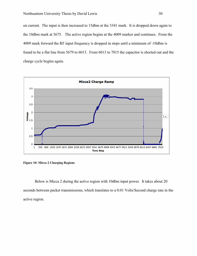
Below is Micca 2 during the active region with 10dbm input power. It takes about 20
seconds between packet transmissions, which translates to a 0.01 Volts/Second charge rate in the
active region.

Northeastern University Thesis by David Lewis 31
Figure 11: Micca 2 Mote Active Harvesting Region
There will be a defined time between transmissions that is dependant on the MCU used,
the energy storage capacitor used, and the received RF power. Minimizing the MCU power
consumption in turn lowers the storage capacitor size and increases the frequency at which the
node can re-transmit data. The RF power input also increases this frequency as the power
increases. From this retransmit time and with the protocol assumptions made previously we can
compute the throughput of the system at a particular RF power input.

Northeastern University Thesis by David Lewis 32
TI Sensor Active Region
0
0.5
1
1.5
2
2.5
3
3.5
1 241 481 721 961 1201 1441 1681 1921 2161 2401 2641 2881 3121 3361
Time Units in 0.5s
Vo
ltag
e
TI Sensor VDD
Figure 12: TI Sensor Active Region Wireless -5dBm
Next the experiment was repeated with a Texas Instruments MSP430 sensor IC’s using
the eZ430-RF2500-SHE platform and an MPA-40-40 4Watt wideband power amplifier from RF
Bay was used to amplify the RF signal generators output and drive a 50 ohm antenna. This is
less accurate as to what power is received by the harvester, but shows the concept. The on board
antenna was used for the harvester. The output shows a 0.001 Volts/second charge rate in the
active region.
From this data one can see the limitations of this type of system. Although the power is
self-sufficient the RF power input required to run the system is substantial. This would limit the
design to a scenario where a base station must transmit power to the devices at 641Mhz and be
active at all times to receive data as it is transmitted on possibly a different frequency band such
as the 915 MHz ISM band.

Northeastern University Thesis by David Lewis 33
2.4: Power Matching Networks:
Because the boost circuit is inherently non-linear the output impedance and input
impedances of the circuit have a non-linear effect on the output voltage. The important factors
that go into the matching network selection are input impedance, output impedance, RF input
power, and RF input frequency. Input impedance is dependant on the antenna used. In most
cases we can assume that 50 or 75-ohm antennas are the expected requirement. Output
impedance, which is dependant on the MCU and capacitor chosen from the study above, is best
measured from measuring the voltage and current of the sensor during particular states of
operation. The important states to measure are sleep, idle, RX active, and TX active. Below is a
table of Micca 2 gathered power measurements and its translation to impedance. From this it
was concluded to run the simulations with a 100kohm load to emulate the MCU load in sleep
mode.
MODE TRANSMIT RECEIVE IDLE SLEEP
CURRENT (mA) 22.00 15.50 3.20 0.03
VOLTAGE (V) 3.00 3.00 3.00 3.00
POWER (mW) 66.00 46.50 9.60 0.09
IMPEDANCE (OHMS) 136.36 193.55 937.50 100000.00
Figure 13: Micca 2 Mote Power Measurements
RF input power changes the impedance of the system as well since when the diodes start
conducting the system lowers in impedance. This means that measuring input power versus

Northeastern University Thesis by David Lewis 34
output power is really the best way to get a read on impedance. A S11 sweep was conducted in
simulation using ADS with the results below.
Figure 14: S11 Sweep for 10 Stage Harvester
RF input frequency also affects the impedance of the design. As input frequency
increases the diode switching characteristics breakdown. RF detector diodes are good at
switching in high frequencies, but still break down in the several GHz range. As the switching
characteristics degrade the impedance of the diode changes dramatically. The diode also has a
built in parasitic capacitor that determines these characteristics. As with capacitors as frequency
increases capacitors become short circuits. One may think that lowering impedance would be
good for power transfer, but as this impedance lowers the voltage multiplier ceases to work.
Since the impedance changes dynamically it is impossible to power match the circuit for
all input frequencies, all RF power levels, and all dynamic load states with passive components.

Northeastern University Thesis by David Lewis 35
One may then assume that dynamic power matching is the best way to go, but unfortunately to
tune the circuit on the fly requires power that tends to be more consumption than the efficiency
gain it provides it in the first place. Because the design is ultra low power harvesting only
passive components can be used for power matching to assume the best efficiency.
The ideal power-matching network is a LC matching network. Whether it is a step up or
step down network depends on the conditions mentioned prior to this. Using ADS the S11
impedance was simulated. Using this impedance and a tuning assistant in ADS simulation was
done to find the best power matching LC network. Even with these simulations manual tuning
was also required to account for board and component parasitics that are not modeled in ADS.
For a 641Mhz 0dbm RF input the series inductor and shunt capacitor configuration is best. For a
915 MHz 0dbm RF input a series capacitor and shunt inductor is best.
2.5: LC Tank Circuit:
If the design needs to be limited to a very narrow band of harvesting this can be
accomplished with a series LC tank circuit with resonance at the given frequency. A tank circuit
with various bands in the DTV regions is calculated in the table below. The LC tank was tested
and does attenuate signals out of the band of interest, but also degrades the performance of the
circuit in the band of interest. We decided against using this circuit for our data, but the
suggested components are provided below.

Northeastern University Thesis by David Lewis 36
Band pass Filter with
LC in series with input
This should be implemented if we only
want 641 MHz power (not everything)
L 0.000001 0.000001 0.000001
C 2.4E-12 2.5E-12 2.3E-12
F 645497224.4 632455532 659380473.4
Figure 15: LC Tank Circuit Parameters
2.6: Printed Circuit Board Design:
The printed circuit board design was to allow for multiple 10 or 7 stage harvesters to be
chained together using board to board interconnections. These board-to-board connectors are
industry standard 0.1‖ headers and plugs that allow for easy connection and disconnection of
each harvester PCB from the other. The board was designed in a way such that each harvester
could be connected on any of the 4 sides of the PCB to another harvester. The connection shares
only the voltage output, which then would be tapped off for the MCU power at some point. To
make sure that each circuit does not interfere with each other’s final stage a blocking diode is
also used. This diode introduces some voltage loss, but is very minimal due to the current flow
in the diode being so low.

Northeastern University Thesis by David Lewis 37
Figure 16: DTV Harvester OrCAD Schematic
The PCB schematic was designed in Cadence OrCAD Capture 16.2. The netlist was
exported to Mentor PADS PCB for layout. The PCB was fabricated at Chicago Interconnect.
Figure 17: Harvester Compared to a Quarter.

Northeastern University Thesis by David Lewis 38
Figure 18: Harvester Antenna Compared to Lip Balm Container.

Northeastern University Thesis by David Lewis 39
Figure 19: Chaining Harvesters Together in a Harvesting Array
One pitfall to LC power matching approach is that the parasitics gathered from the PCB
are on the same order of magnitude as the simulated ideal matching components. Each trace on
the board is a transmission line with RLC components. The resistance is minimal for our short
traces, but the inductance is around 43 nH per inch and capacitance is closer to 216 fF per inch of
trace. When simulated ideal match at 915 MHz is with a less than 5 nH of inductance, and there
is already more than that in parasitic components, one has a problem matching for an ideal case.
Mitigating the parasitics was attempted by fabrication of a second PCB. The PCB was
designed in Cadence OrCAD Schematic Capture, and PADS layout. Footprints for the

Northeastern University Thesis by David Lewis 40
components used were drawn as part decals and saved into a reusable library. OrCad symbols
for components were custom drawn for diodes and antenna. Standard symbols used from
Cadence were inductors, and capacitors.
For minimizing component parasitics 0402 sized surface mount inductor and capacitor
sites were used for LC matching network. Using a smaller package size minimizes ESR and
ESL components of matching network capacitors and inductors. High Q RF inductors were
purchased to minimize losses during power and antenna matching stages.
For minimizing trace parasitics the stack up and trace width was chosen to decrease
parasitic capacitance. The trace width was made smaller, but at the same time not so small that
resistance was increased. Picking 25-30 mils on a 62-mil thick board with ½ OZ copper from
simulation seemed to show close to ideal efficiency matching. The inductances were still too
high, but lengths of the traces were minimized as best as possible. To get to 5nH only around
200 mils of total trace would be allowed and this is impossible with the component keep out and
design requirements.
The resistance of the trace can be calculated using the resistivity of copper (1.7E-6 ohm-
cm) and assuming 25C for our calculations. L is length of the trace, W is width of the trace and
T is the thickness of the trace.
Figure 20: PCB Resistance Calculation
Simulation of resistance, inductance, and capacitance values were all done in Mentor
Graphics Hyperlynx and are shown below.
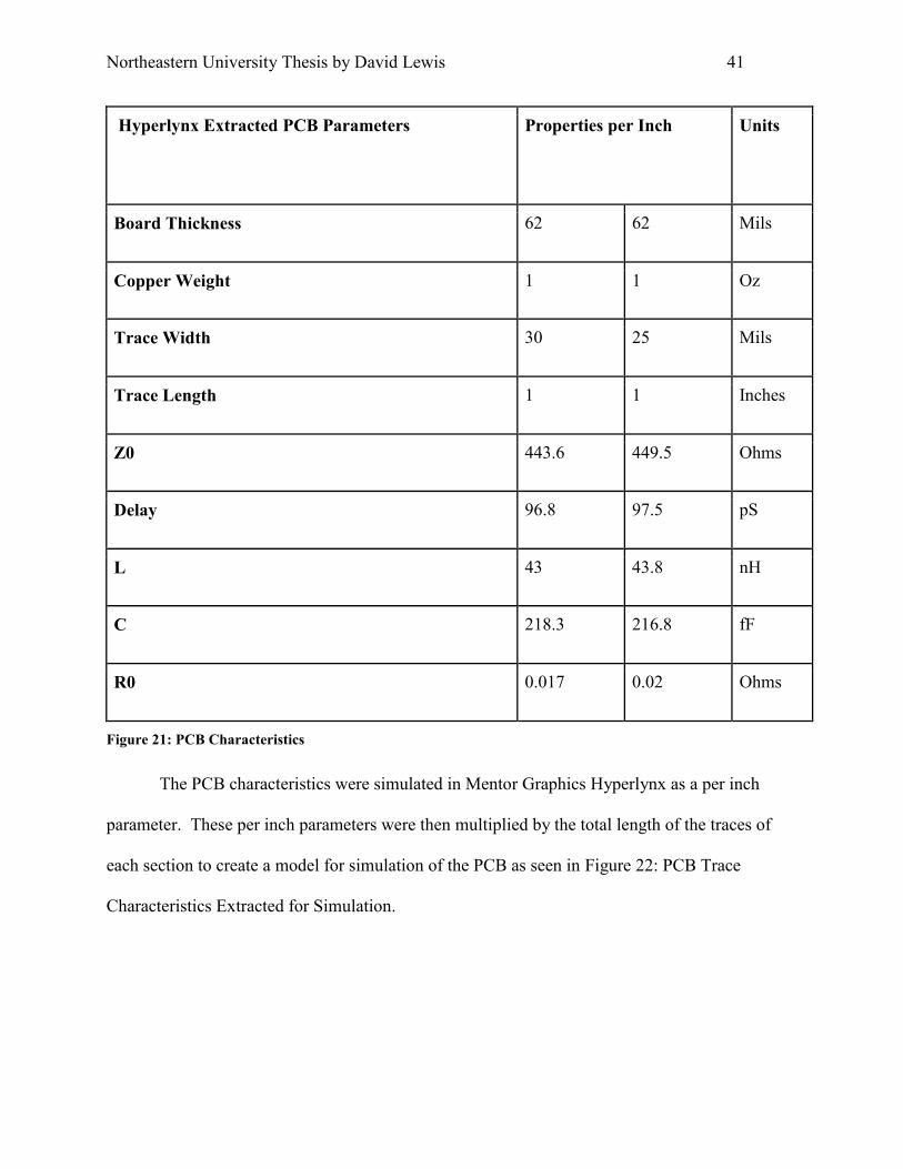
Northeastern University Thesis by David Lewis 41
Hyperlynx Extracted PCB Parameters Properties per Inch
Units
Board Thickness 62 62 Mils
Copper Weight 1 1 Oz
Trace Width 30 25 Mils
Trace Length 1 1 Inches
Z0 443.6 449.5 Ohms
Delay 96.8 97.5 pS
L 43 43.8 nH
C 218.3 216.8 fF
R0 0.017 0.02 Ohms
Figure 21: PCB Characteristics
The PCB characteristics were simulated in Mentor Graphics Hyperlynx as a per inch
parameter. These per inch parameters were then multiplied by the total length of the traces of
each section to create a model for simulation of the PCB as seen in Figure 22: PCB Trace
Characteristics Extracted for Simulation.

Northeastern University Thesis by David Lewis 42
PCB Trace
Characteristics
From
Antenna to
Match
From Antenna
Match to
Power Match
From Power
Match to
Harvester
(25mils)
Total Units
Trace Length 1.429 0.536 0.222 2.187 inches
Z0 443.6 443.6 449.5 445.5666667 ohms
Delay 138.3272 51.8848 21.645 211.857 pS
L 61.447 23.048 9.7236 94.2186 nH
C 311.9507 117.0088 48.1296 477.0891 fF
R0 0.024293 0.009112 0.00444 0.037845 Ohms
Figure 22: PCB Trace Characteristics Extracted for Simulation
The new PCB design with 641 MHz stimulus showed a 2x improvement in open circuit
voltage from the previous PCB. It was thought at first to shorten the PCB traces as much as
possible to prevent losses so this is how the board was fabricated. It was found after production
of the PCB through simulation that it is actually better to have slightly longer traces to tune to a
particular frequency. A future PCB would use the trace lengths described in simulation to match
to a particular frequency without requiring external matching components to increase efficiency.

Northeastern University Thesis by David Lewis 43
2.7: Simulation Results:
Simulations were preformed using Agilent ADS 2009. Spice models were used for the
diodes and passive components. A schematic of the simulation including PCB parasitics is
shown below. To model the transmission line of the PCB an LC network was used. Hyperlynx
simulation environment from Mentor Graphics was then used to extract from the actual layout
the transmission line characteristics. With these extracted values simulation matches real life
measurements in a relatively close manner.
The only major mismatch with simulation and actual measurements are the inductor and
capacitor models used for matching. The components that are purchased from Mouser or
Digikey are far from ideal and their datasheets do not provide a decent model range to use for the
components. Using Kemet spice gets you fairly close for capacitor simulation, but the RF
inductors used did not have models to use for simulation. The component variance tended to be
a problem anyway. The same components on different PCB designs tended to show different
matching frequencies, which show that they cannot be fully relied upon for the matching circuit.
Below is a schematic draw in Agilent ADS used for simulation. There are two harmonic
balance simulations and four sweep parameters for various simulations. It should be noted that
efficiency uses an equation variable that does not change based on the input value, therefore
simulations that use more than one stage show a non-real efficiency percentage. For instance a
dual stage efficiency ideal would have been 200% and a quad stage would have been 400%.

Northeastern University Thesis by David Lewis 44
Figure 23: 10 Stage Schematic With PCB Parasitics
Northeastern University Thesis by David Lewis 45
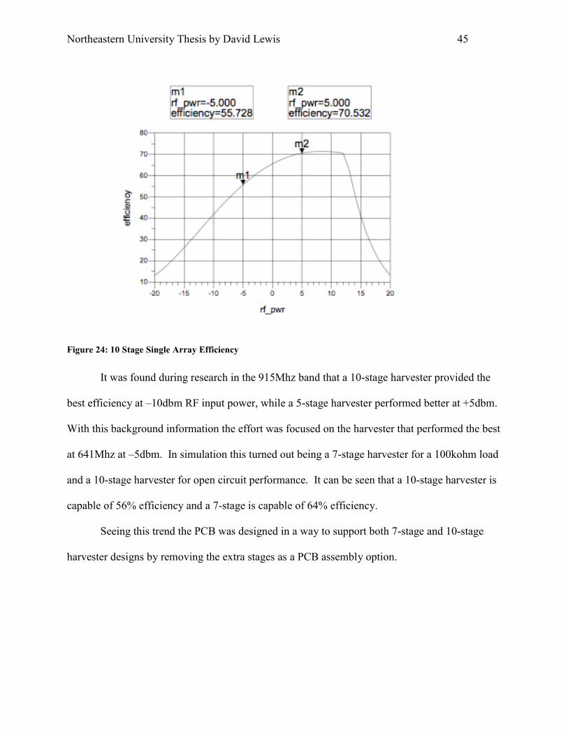
Figure 24: 10 Stage Single Array Efficiency
It was found during research in the 915Mhz band that a 10-stage harvester provided the
best efficiency at –10dbm RF input power, while a 5-stage harvester performed better at +5dbm.
With this background information the effort was focused on the harvester that performed the best
at 641Mhz at –5dbm. In simulation this turned out being a 7-stage harvester for a 100kohm load
and a 10-stage harvester for open circuit performance. It can be seen that a 10-stage harvester is
capable of 56% efficiency and a 7-stage is capable of 64% efficiency.
Seeing this trend the PCB was designed in a way to support both 7-stage and 10-stage
harvester designs by removing the extra stages as a PCB assembly option.

Northeastern University Thesis by David Lewis 46
Figure 25: Ideal 7 Stage Single Array Efficiency
After simulations with an ideal 80kohm load 100kohm was also simulated to match the
MCU current draw during sleep mode. Using this mode it was found that efficiency could drop
substantially with PCB parasitics included, but did not make much difference if the parasitics
were not included.

Northeastern University Thesis by David Lewis 47
Figure 26: 10-Stage 100kohm Load Using Extracted PCB parasitics
Figure 27: 10-Stage 100kohm Load Using Extracted PCB Parasitics Matched with 1.9pF and 25nH
Changing the matching components at open circuit conditions could also strongly
influence the efficiency. Given these statements it is clear that matching must be done in a way
specific to both the input impedance and load impedance a particular frequency. It must also be
mentioned that finding an exact match in impedance does not provide the best power delivery.
One must target a 2:1 ratio to provide best power transfer. With this known it was found that

Northeastern University Thesis by David Lewis 48
matching actual passive components was difficult because of their inherent parasitics. In a
design as sensitive as this there needed to be a way to avoid this weakness. SSTEP protocol
described later in this thesis provides a way around this issue.
Figure 28: Finding Ideal Trace Length for 641Mhz
Once the PCB parasitics were extracted it was clear they should be used for matching the
design. A simulation was run to find the ideal trace length for the trace segments used to connect
the stages of the harvester array. The simulation revealed that the 250mils used to minimize the
trace parasitics should have been lengthened to 400mils for ideal matching. In future PCB
designs this metric should be used to hopefully remove the need for extra matching components.

Northeastern University Thesis by David Lewis 49
Figure 29: Frequency Sweep of Unmatched PCB with 250mil Trace Lengths
A frequency sweep of the unmatched PCB was run to compare against the measured
results. It was found that in simulation 250Mhz would perform the best on the PCB that was
fabricated and that 650Mhz was actually one of the worst performers. This does not match the
recovered results for the unmatched case perfectly at 650Mhz and 950Mhz, but did correctly
predict the frequency peak effects that were observed. The peaks just appeared to be shifted
upwards slightly. Refer to Figure 46: Harvester Open Circuit Voltage Versus Frequency for a
plot of the measured results. Below is a table of the comparison between the expected voltage
from simulation and the actual voltage at three points of interest.

Northeastern University Thesis by David Lewis 50
Frequency Simulation Measured
250 6.57 6.5
650 1.39 3.22
950 5.09 3.38
Figure 30: Comparison Between Simulation and Measured Voltages at Certain Frequencies
Figure 31: Frequency Sweep of Unmatched PCB Voltage Versus Frequency
A comparison of frequency sweep simulations shows that for a sweep of frequencies
from 100Mhz to 1Ghz the best energy transfer point for the unmatched circuit is 250Mhz. The
second best is 900Mhz. In real measurements 300Mhz was the lower peak and the next peak
does not occur until 1.2Ghz. This shows that the simulation is close, but still lacks perfect
correlation with the PCB.

Northeastern University Thesis by David Lewis 51
Figure 32: Dual Array 10 Stage Harvesters (Efficiency x2)
It was found that to improve total power consumption that more area needed to be used.
Since the energy density of RF power in air tells us you can harvest more power if you harvest in
a larger area, it seems logical to try to increase the harvesting area to increase the amount of
power harvested. A dual stage and quad stage array of harvesters were simulated to see how
much improvement could be obtained. Unfortunately there is not a 2x improvement for doubling
the amount of harvesters used because of the adverse effects on the other harvesters, but
simulation ideally shows a 1.6x improvement by doubling the amount of harvesters in the array.
The efficiency number used in the graphs is based on the original input RF power for simulation,
therefore the actual efficiency shown in the dual stage simulation is half of the number plotted.

Northeastern University Thesis by David Lewis 52
This means that as you increase the number of harvesters the efficiency decreases on each
harvester, but the total power harvested does increase as more harvesters are added.
Figure 33: Quad Array 10 Stage Harvester (Efficiency x4)

Northeastern University Thesis by David Lewis 53
Figure 34: Quad Array 7 Stage Harvester
After it was found that there exists a startup current surge that an MCU requires to startup
caused by a minimum voltage ramp rate to prevent transistor latch a MPPT regulator was
researched. The MPPT regulation benefits seem to fit this design perfectly. The only problem
was that the input impedance that the regulator presented to the design was 6kohms.
Unfortunately this is a heavy loading for this type of circuit. Simulations were run to determine
the performance of the design with a 6kohm load.

Northeastern University Thesis by David Lewis 54
Figure 35: 10 Stage with 6kohm Load Simulating MPPT Regulator
It was discovered that the efficiency drops from 56% on a 10-stage design to 6% with the
matching used for 100kohm loading. It was then attempted to rematch the circuit via simulation.
After simulation only 27% efficiency at 10-stage circuit could be obtained. This unfortunately is
not enough to power the MPPT regulator.

Northeastern University Thesis by David Lewis 55
Figure 36: 10 Stage with 6kOhm Load 4pF and 10nH Match
Figure 37: 10 Stage 6kOhm Load with 2pf and100nH Match

Northeastern University Thesis by David Lewis 56
Simulation was then steered in a direction to decrease the number of harvester arrays to
increase the efficiency with this low output load. Decreasing the harvesting arrays tends to
improve heavy loading conditions, but it also tends to the decrease the voltage harvested. The
target voltage to harvest is 2.5v and above for typical sensor MCU’s. Ideally 3.1v-4.1v would be
the best voltage range to harvest at to look similar to a single cell lithium ion battery.
Figure 38: 7 Stage 6kOhm Load With 5nh and 5.5pF Match

Northeastern University Thesis by David Lewis 57
Figure 39: 7 Stage 6kOhm Load With 2.6pf and 3uH Match
Figure 40: 5 Stage 6kOhm Load With 5pF and 0nH Match

Northeastern University Thesis by David Lewis 58
Figure 41: 2stage 6kOhm Load With 0.6pF and 15nH Match
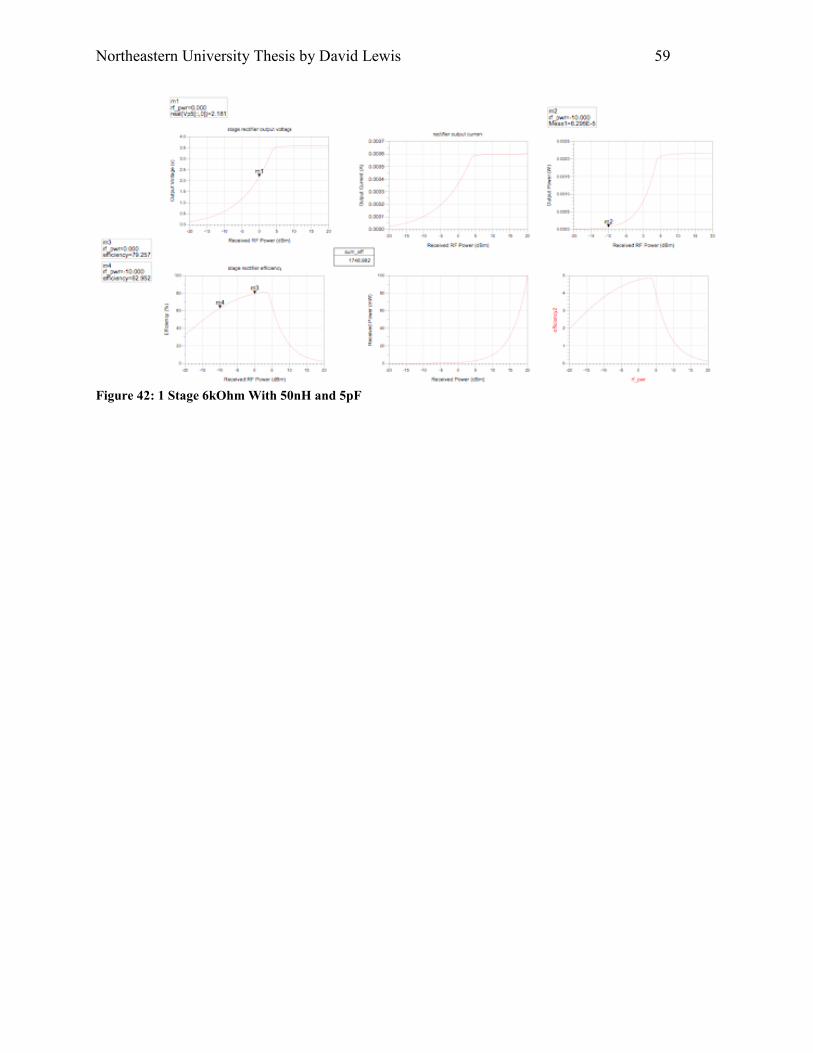
It was found that the best that could be done was a 1-stage harvester with 62% efficiency.
The power simulation finds that the ideal 1-stage could harvest about 62uW of power for the
MPPT regulator at –10dbm. Unfortunately this provides only 2.181 Volts total voltage at –
10dbm. This is unacceptable for the application of powering a MCU with a 2.5V VDD.
Northeastern University Thesis by David Lewis 59
Figure 42: 1 Stage 6kOhm With 50nH and 5pF

Northeastern University Thesis by David Lewis 60
Chapter 3: Design Optimization for Ultra Low Power Applications
3.1: Using a Harvesting Cell Array to Increase Power:
A key improvement to this design is increasing the number of antennas used to harvest
more power from the same frequency band. The concept is similar to solar cells in that
increasing the area of cells increases the energy harvested. The energy density of a particular
frequency tells one what type of area is required to harvest a particular amount of energy. The
design must then be created into a cell. Inside this cell is the harvesting circuit proposed as well
as an antenna capable of receiving in the 641 MHz band. A PCB was fabricated for this purpose
by utilizing a Fractus FR01-B1-S-0-047 digital TV antenna. The PCB was built in a way to have
board-to-board connectors on all 4 edges such that additional PCB’s can be attached to build an
array of harvesters in the same plane.
To connect the boards together and not adversely affect the 10th diode stage of the
harvester an additional steering diode was used to block interference from another harvester.
The diode would only allow the highest voltage harvester to conduct to the output, but would
increase the current capability since more harvesters gathering approximately the same amount
of energy are summed together. This does not lead to a voltage increase in the output, but does
increase current capability. Choosing the lowest drop diode here is the key metric, but also
picking a low loss diode must be kept in mind.

Northeastern University Thesis by David Lewis 61
Figure 43: Ideal Harvester Array Concept
In the ideal case all the cells of the array are tuned to exactly the same peak frequency,
but in real life due to variances in the components of the design this is not normal. The range of
variance can be up to 50Mhz.
The addition of a cell to the array is not a direct doubling of power harvesting. Each
additional harvester will only add between 10%-50% more power to the overall circuit when
going from one board to two. Because of this the amount of cells required to substantially
increase total power is fairly high. This approach however is required for extremely low ambient
energy density scenarios.

Northeastern University Thesis by David Lewis 62
Figure 44: Projected Number of Harvesters in Array Versus Power Harvested
As the number of harvesters in the array increases the power increases, but because of the
degradation of each harvester in the array caused by adding more harvesters the power
relationship is logarithmic. As more harvesters are added the efficiency of the circuit decreases
logarithmically. This is all assuming that all of the harvesters are matched perfectly. In practice
this is not true and each harvester takes even more efficiency loss when a harvester is not
matched properly. A single harvester with poor matching compared to other harvesters could
hurt the array more than it helps.

Northeastern University Thesis by David Lewis 63
Figure 45: Efficiency Versus Number of Harvesters In Array
3.2: Using a Multiple Band Antenna to Harvest More Energy:
Another improvement is using multiple frequency bands to harvest energy. The
harvesting circuit proposed naturally has voltage peaks at RF input frequencies of 400Mhz and
2.1Ghz. These peaks are based on resonances of the PCB design and component selections.
When we match the circuit to 641 MHz we are moving the lower voltage peak from 400Mhz to
641 MHz. By using two RF input frequency sources we can almost double the amount of power
to harvest. To test this we insert two tones, one at 400Mhz and one at 2.1Ghz, each at 0dbm into
the harvesting circuit. By doing this we see a close to doubling in voltage at the output. This
relates to doubling the RF input power of the circuit. To fully accommodate this input one must
use a dual band antenna to harvest at several frequencies.

Northeastern University Thesis by David Lewis 64
The voltage received at the output is very close to the individual components added. For
instance when 400Mhz at 0dbm is inserted into a circuit one measures 1.59v. When just 641
MHz is provided at 0dbm the open circuit voltage measures 4.26v. When the two frequencies
are combined and provided to the input, each at 0 dBm, the open circuit voltage of the harvester
reaches 5.12v. This means that a similar power amplifier can be used for the output of the base
station instead of a single larger power amplifier for 1 frequency. Because of this we can almost
double our harvested energy.
A survey was constructed to slew the input frequency at 0 dBm power, while measuring
the open circuit output voltage. The results are a shown in the graph below for the various
circuit matches used.
Figure 46: Harvester Open Circuit Voltage Versus Frequency

Northeastern University Thesis by David Lewis 65
It can be seen from this data that the unmatched circuit has 3 major peaks in its harvested
energy. When adding matching components we shift and possibly amplify this voltage. The
more capacitance added in shunt shifts the peaks down in frequency. The series inductive
portion allows amplification near the roll-off. It was found that a series inductance of 8.2nH and
a 9.1pF shunt capacitor gave the best results for 641 MHz. It also decreased a large spike of
voltage around 1.4 Ghz. A better choice for multi-band harvesting is using just a 10pF shunt
capacitor and relying on the pre-existing 43nH parasitic in the traces. This choice gives good
voltage at 641 MHz and also amplifies the voltage spike around 1.4Ghz. Using this matching
technique could then be used to amplify several frequencies that can be used for harvesting with
a multiple band antenna.
As this project evolved it was found that someone else has the same idea and proposed an
antenna capable of it in December [17], but does not appear to have done any integration with a
sensor to overcome the many issues faced. The design is however exactly what this work would
have proposed as a future work. By choosing the multi-band antennas for the frequency bands
allowed by the FCC and then following the tuning procedure one can find a best fit harvesting
circuit. Once this circuit is ideal it can be replicated into multiple antenna arrays at half
wavelength distances for board to board connections. This even further increases the energy
gathered and hence shortens the charge cycles. Since -10dbm was measured on the Micca 2
sensor mote without these additions it could be as little as -20dbm input power required to
maintain the MCU in sleep mode. Other MCU’s with even smaller current consumption can
then use smaller supercapacitors and can be used for even better charge times.
Charge times were measured against a 100mF supercapacitor loaded with 100Kohm load
in parallel for a 0v to 1.8v ramp. The input power was introduced by the RF signal generator
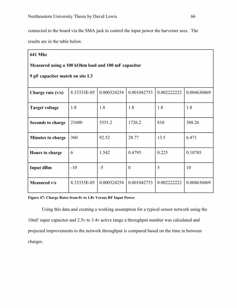
Northeastern University Thesis by David Lewis 66
connected to the board via the SMA jack to control the input power the harvester sees. The
results are in the table below.
641 Mhz
Measured using a 100 kOhm load and 100 mF capacitor
9 pF capacitor match on site L3
Charge rate (v/s) 8.33333E-05 0.000324254 0.001042753 0.002222222 0.004636069
Target voltage 1.8 1.8 1.8 1.8 1.8
Seconds to charge 21600 5551.2 1726.2 810 388.26
Minutes to charge 360 92.52 28.77 13.5 6.471
Hours to charge 6 1.542 0.4795 0.225 0.10785
Input dBm -10 -5 0 5 10
Measured v/s 8.33333E-05 0.000324254 0.001042753 0.002222222 0.004636069
Figure 47: Charge Rates from 0v to 1.8v Versus RF Input Power
Using this data and creating a working assumption for a typical sensor network using the
10mF super capacitor and 2.5v to 3.4v active range a throughput number was calculated and
projected improvements to the network throughput is compared based on the time in between
charges.

Northeastern University Thesis by David Lewis 67
Figure 48: Throughput Versus RF Input Power
The antenna was then matched on a PCB with no load. It was found that the suggested
components from the manufacturer needed adjustments. Below is the matching results based on
maximizing received RF power.
Matching components with 20bm output at antenna 6 inches away from source DB
No match -25
10 nH shunt -33
8.2 nH series + 10nh shunt -28

Northeastern University Thesis by David Lewis 68
10 nH series + 8.2nH shunt -30
1.8 nH shunt -42
6.2 nH series + 1.8 nh shunt -44
22 nH shunt -24
12 nH shunt -25
12 nH series + 12 nH shunt -26
22 nH series + 22 nH shunt -26
1.8 nH series + 22 nH shunt -22
1.8 nH series + 12 nH shunt -26
0.3 nH series + 22 nH shunt -26
3.3 nH series + 22 nH shunt -18
12 nH series + 22 nH shunt -20
4.7 nH series + 22 nH shunt -20
2.7 nH series + 22 nH shunt -21
3.9 nH series + 22 nH shunt -17
Figure 49: Antenna Matching Results

Northeastern University Thesis by David Lewis 69
It can be seen that even with matching the antenna used although small form factor does
not gather much input power. Using a different antenna with more gain would be optimal for
minimizing charge times.
Efficiency Units Notes
Path loss efficiency 2.50% % At 20m 4W 641Mhz
Antenna efficiency 0.0798104 % At 1m 1W 641Mhz
Harvester efficiency 70% %
Regulator efficiency 90% %
Total system efficiency 0.0125685 %
Figure 50: Total System Efficiency
Charge times were then measured with the antenna chosen for four boards. The four
boards were then combined in an array and charge rate increase was measured. It was found that
the arrays increase the charge rate and hence gather more energy. It was found that 3 of the four
boards did the majority of the work, while one board seemed to be less efficient. It was also
found that looping the antenna array had adverse effects on the RF power received and hence
should be avoided.
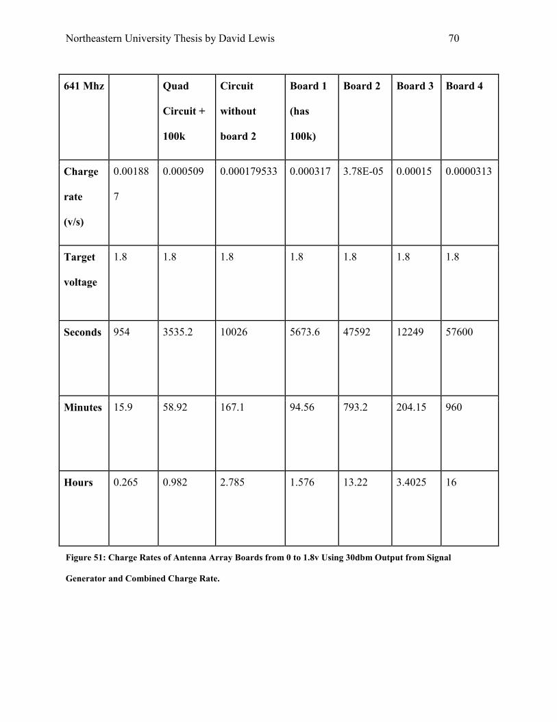
Northeastern University Thesis by David Lewis 70
Figure 51: Charge Rates of Antenna Array Boards from 0 to 1.8v Using 30dbm Output from Signal
Generator and Combined Charge Rate.
641 Mhz Quad
Circuit +
100k
Circuit
without
board 2
Board 1
(has
100k)
Board 2 Board 3 Board 4
Charge
rate
(v/s)
0.00188
7
0.000509 0.000179533 0.000317 3.78E-05 0.00015 0.0000313
Target
voltage
1.8 1.8 1.8 1.8 1.8 1.8 1.8
Seconds 954 3535.2 10026 5673.6 47592 12249 57600
Minutes 15.9 58.92 167.1 94.56 793.2 204.15 960
Hours 0.265 0.982 2.785 1.576 13.22 3.4025 16

Northeastern University Thesis by David Lewis 71
From this data we can then determine the improvements to network throughput. Using
the same assumptions from Figure 5: Protocol Requirements we can determine a throughput
number for each board and for quad board configurations.
Figure 52: Throughput Versus Array Size 641Mhz 0dbm
It can be seen from this plot of throughput that board 1 contributes the most to the quad
output at 641Mhz and with 0dbm RF input power. However, it should be noted that use of the
SSTEP energy transfer protocol more evenly distributes the contributions from mostly one board
to all boards.

Northeastern University Thesis by David Lewis 72
Chapter 4: Network Optimization for Ultra Low Power Applications
4.1: Spread Spectrum Transfer Energy Protocol (SSTEP)
Noticing the effects of the frequency peaks and tuning effects from board to board led to
a proposed protocol for energy transfer for charging. The protocol leverages spread spectrum
tables from the base station and builds a spreading table for energy transfer to the sensor nodes.
Since each node may have different frequency peaks for maximum efficiency we need to build a
spread table that includes these peaks. The protocol requires two frequency bands. The first
band is a communication carrier, which in our case is the ISM 915 MHz band and an energy-
harvesting band, which is 580-700 MHz. The harvesters have already been optimized based on
MCU selection and capacitor selection to maximize charge ramp rates.
This protocol proposed is implemented only up to the link layer, but is capable of being
scaled for a more complete stack. The protocol is flexible enough to allow a single frequency
band to be both the charging and communication channel using time slots, but this is not
implemented because of the efficiency losses associated with this technique. In [21] the authors
propose a protocol that uses weights for each node in the routing tables that includes a measure
of energy consumption. In our case the consumption is assumed to be the same, but we do want
to assign weights based on the energy gathering rates. If one node is capable of harvesting two
times more energy than that of another node and each node consumes the same amount of energy
to transmit than the weaker charging node must be weighted higher in the spreading table to
ensure it will deliver data at a somewhat reasonable frequency.
The routing protocol is not implemented, but the protocol in [21] still would be a good
candidate for the routing protocol to stack on top of the proposed link layer. AODV is a popular
routing choice for this type of network because of its flexibility. Each node forwards all packets

Northeastern University Thesis by David Lewis 73
and the fastest path to reach the destination is the path chosen for return. This is useful and
simple for a constantly changing network of nodes that will be dead or alive at an unknown
probability. This however has a limitation of wasting transmission of nodes that are known to
have poor energy harvesting capabilities.
When building a sensor network there are several conflicting goals. In [31] it was found
that the lifetime of a network of nodes powered by super capacitors is decreased by the amount
of charge and discharge time used. If the network uses short charge times the throughput of the
network increases, but lifetime of the super capacitors is decreased. This design tradeoff can be
accommodated in SSTEP by setting the thresholds of operation for the nodes to the maximum
value for increased lifetime, or decreasing the transmission level to a lower voltage to increase
throughput. Throughout this discussion it is assumed that lifetime of the network is more
important than throughput.
The protocol achieves many new possibilities for a wireless sensor network. Some of the
more interesting possibilities are listed below.
Ability to maximize power harvesting efficiency to all nodes on network.
Provides a way to have as many nodes come alive as possible simultaneously using
charge time prediction. This allows for node-to-node communication with as much of an
active network as possible. This is called charge time synchronization.
Allows for selective node peak efficiencies for nodes that may be of more importance to
the overall network.
Allows multiple base station communication to prevent frequency cancellation between
shared nodes.

Northeastern University Thesis by David Lewis 74
Adds a capability to change network throughput on the fly at the cost of network lifetime
losses.
Provides a way to minimize collisions on the network by using charge time prediction to
prevent multiple sensor nodes from coming alive and transmitting simultaneously. This
is preferred for a one-way network where each node is just transmitting to the base
station.
As mentioned earlier it was found that the matching of the arrays limits their ability to be
used together. All the nodes in the array will exhibit different matching based on the
component tolerances. In figure below our ideal harvester array is broken down into a closer
to real life scenario where not all of the harvesters are matched to the same frequency. This
degrades the performance of the overall circuit and hurts efficiency.
Figure 53: SSTEP Protocol Improving Harvesting Arrays

Northeastern University Thesis by David Lewis 75
STTEP protocol can be used in this scenario to improve the efficiency of this array. It
can be seen that there are the following cells types and counts:
11 Harvesters Matched to 610Mhz (green)
2 Harvesters Matched to 620Mhz (orange)
6 Harvesters Matched to 630Mhz (red)
4 Harvesters Matched to 640Mhz (blue)
2 Harvesters Matched to 650Mhz (yellow)
Assuming the harvesters are all the same orientation and distance from the RF power source,
when a 610Mhz signal is applied to the array 11 out of 25 harvesters will perform well, while 14
out of 25 may not perform well at all and will actually drive down the performance of the 11 at
peak efficiency. With SSTEP protocol a spread table of 25 values can be created with 1 value
for each harvester. What this would do is create the following frequency percentages.
11/25 of the total time the transmission frequency will be 610Mhz
2/25 of the total time the transmission frequency will be 620Mhz
6/25 of the total time the transmission frequency will be 630Mhz
4/25 of the total time the transmission frequency will be 640Mhz
2/25 of the total time the transmission frequency will be 650Mhz
This results in the following spread RF output:

Northeastern University Thesis by David Lewis 76
Figure 54: SSTEP RF Output Frequency Spread
Using this spreading function can maximize the power harvesting efficiency by adding
more weight to each point. The protocol can also maximize the time that all the sensor nodes of
the network are alive by weighting certain nodes that take longer to charge higher. This gives
their particular frequency matching more power and lessens the importance of closer nodes until
a time balance is met between the two.
4.1.1: Discovery Phase:
To build a table of frequency values that allow peak efficiency for each sensor we must
first find the charge ramp time that each sensor node is getting from a start frequency. During
the discovery phase the base station will transmit at a fixed frequency of 614 MHz, which is the

Northeastern University Thesis by David Lewis 77
low end of the DTV band. The sensor when reaching its min charge threshold starts a timer and
begins sampling its battery voltage until it reaches the max charge threshold. Once the max
active threshold is reached the sensor mote will calculate the time it took to reach its max active
threshold from its minimum active threshold and transmit the data to the base station. This data
will be transmitted every time to ensure that spread tables are constantly updated. During
discovery this is the only information the sensors will transmit.
Using this data the base station will then increase its energy harvesting band transmission
frequency and again wait for all the known motes to update their charge ramps. At each
frequency of transmission the base station will store an array of known motes and their charge
times. A fixed length of time must be used to start with during discovery. Using the delta values
from each mote the base station must build a table of frequencies for each node’s best charge
time. The base station will continue to increase the frequency until the maximum band
frequency is reached (698 MHz). At this point in time a table will have been built with a set of
frequencies that provide best efficiencies for each mote. If there are several motes that exhibit
their best efficiency at the same frequency then that frequency value will receive a higher
periodicity in the spread table.
Since all the nodes must reach max threshold to transmit each node is responsible to clear
its voltage to minimum threshold when the base station changes frequency. The base station is
responsible to broadcast a change frequency beacon for 2 minutes to ensure all sensors see the
change. The beacon will have a change frequency message and a time stamp to allow the sensor
to synchronize with the base station. Since some nodes in the network will be dead or not in an
operational state during discovery they are assumed to be below the operational threshold and
will not be found until they reach at least the minimum threshold. The nodes when reaching the

Northeastern University Thesis by David Lewis 78
minimum threshold then are required to turn on their radio receiver every 1 minute to ensure that
if the base station has changed transmission frequency it sees the change and returns to minimum
threshold by doing an energy dissipation routine. This in our case is just enabling an on board
LED to dissipate back down to minimum threshold.
Using the time stamp the sensor node will know how far into the change frequency
broadcast the base station is. It then from that will start a timer to determine when to start
charging again. It does this by dissipating to the minimum threshold, sampling again and
dissipating again to the minimum threshold until the broadcast timer is expected to have expired.
With this method the node’s internal timer is synchronized with the base station’s timer. This is
critical for real time operation.
After the frequency change has been completed the sensor is expected not to transmit
until it reaches max threshold. The base station after the frequency change only listens for
incoming node messages and builds its frequency table. The discovery phase is complete when
the max frequency of the band is hit. The relative sensor thresholds can be seen in the figure
below. The voltage step will change based on the sensors charge ramp time, but the period of
sampling will always be the same at once every 5 seconds.

Northeastern University Thesis by David Lewis 79
Figure 55: Voltage Thresholds Used For Node States
4.1.2: Active Phase:
During the active phase the base station will transmit power using its spreading table to
modulate the frequency it is transmitting at. This phase will continue until a new sensor is found
and a discovery phase is required. This strategy also allows the spread table to be updated on the
fly allowing a much more flexible design. If a sensor node suddenly has a large difference in
charge times it can be determined that the node has moved location or a new obstruction was
introduced and a discovery phase can be called again to determine its new best frequency. This

Northeastern University Thesis by David Lewis 80
can be useful if nodes periodically will be moved or detrimental environmental factors can occur
periodically.
The base station will apply two values as weights for the spread table. The first is how
many nodes are in that frequency band. The second is the delta charge time, which is used to
determine how long it will take for each node to charge at their peak efficiency frequency. The
goal of the network is to avoid collisions when nodes become active. The protocol can do this
by changing the spread table to space out times when each node becomes active. With expected
time deltas from the sensors discovered in discovery mode the base station can allot slots for
specific sensors it wants to collect data from at a higher periodicity. For our experiment collision
avoidance is the main goal although the protocol would allow for selective charging of nodes.
The sensors in the active phase will be allowed to transmit their data to the base station
when the max threshold is reached and continue to transmit until min threshold is reached.
When min threshold is reached the sensor must return to sleep and wait for max threshold again
before transmitting again. During this period it again measures the amount of time it takes to go
from min threshold to max threshold to sense network changes.

Northeastern University Thesis by David Lewis 81
Chapter 5: Integration of the Design Into 45nm CMOS Technology
Since this design incurs many PCB parasitics integration of this design into CMOS
technology seems like an interesting path to pursue.
Unfortunately the current design is not reasonable to design into an ASIC. Assuming that
one would leave the antenna external to the chip is a must. The antenna design is much too large
to integrate into any ASIC. The cascode charge pump as it stands is also not reasonable, because
the 36pF capacitors are much too large to integrate into silicon. This means that the charge
pump would need to be redesigned as a charge redistribution network with much smaller
capacitors or a single external capacitor that can be much larger. The inductor as well is much
too large to integrate on chip and even with simulation of this component using OTA’s the
quality of this component is degraded. The inductance however can be left external to the design
and combined with the bondwire inductance and an on-chip OTA for automatic tuning the series
inductor could be accommodated.
The cascode diode stages can be integrated fairly easily using MOSFETs in a standard
diode configuration. One would use NMOS transistors with gate tied to drain to emulate a diode.
The source would act as the cathode, while the gate and drain would act as the anode.
There are, however, different possible IC approaches made for RF harvesting design like
that of the one in [18]. This type of design is a better fabrication approach than that of the circuit
proposed in [19].

Northeastern University Thesis by David Lewis 82
Chapter 6: Conclusion and Future Research
6.1: Conclusion
In this thesis we have made a strong applications case for optimizing RF energy
harvesting nodes in the digital TV band. New concepts of harvesting arrays, multi-band
harvesting, and an energy transfer protocol were proposed.
Harvesting arrays could increase the power harvested enough for RF energy harvesting to
become more useful to applications that cannot work in such a power starved environment. With
even more improvements in efficiency the number of harvesters required in the array to produce
1 watt of power may decrease from the current projection of 300,000 cells.
Multi-band antennas could be implemented with the design to harness the tuned
frequency efficiency peaks and provide the same output power by transmitting less power in two
different frequency bands. This improvement can allow cognitive radio applications for energy
power transfer in selected bands as to no interfere with other nearby networks.
The proposal of SSTEP protocol provides a way to increase the network bandwidth,
while at the same time solve the frequency matching problem that these harvester arrays face.
By using modulation of certain tuned frequencies the protocol can provide weighted power
delivery to all nodes of the network. In this way the protocol can maximize the time that the
majority of the nodes in the network are alive at the same time. SSTEP also provides selectivity
to allow certain nodes to be prioritized to charge either more or less for other more unique node
applications.
Northeastern University Thesis by David Lewis 83
6.2: Future Research
Future research would cater to further improving efficiency of the harvester arrays by
exploring antenna design. It would also serve well to create a multi-band antenna for testing
frequency hopping between key bands of interest.
Improving the harvesting array structure as to decrease the efficiency losses sustained by
each node would be a requirement. The spacing of the antennas between each harvester would
also need to be simulated and tested. The array spacing would ideally be as far away from each
other as possible to decrease each others antenna interference, but at the same time a small
distance like a half or quarter of the wavelength is probably enough to accomplish this goal.
The MPPT regulator chosen was too high of a load for a single harvester circuit. In
further research a MPPT regulator should be designed with a very high input impedance, ideally
greater than 80kOhms.
Although the proof concept has been completed, the SSTEP protocol is vastly untested
with actual sensors connected to harvesters or harvester arrays. The MAC protocol must be
finalized and a throughput measurement must be taken to show its true merits.
6.2.1: Implementation of SSTEP protocol
The protocol is currently implemented on Texas Instruments MSP430 sensor IC’s using
the eZ430-RF2500-SHE platform. The base station will be implemented using a sensor node
connected to a host PC via USB. The connection will allow the MSP430 to communicate with
the python application to control the USRP2. The python application is fairly simple and has
already been implemented. It requires a variable frequency source that is accessible to the

Northeastern University Thesis by David Lewis 84
MSP430 via USB. It also requires a USRP2 sink with a matching variable input to that of the
frequency source.
Figure 56: SSTEP Test Platform
This program was tested using a simple GUI with control of the amplitude of the output
signal via a slider and a frequency slider to control the frequency range from 600Mhz to
700Mhz. Using a spectrum analyzer the program was verified to change frequency and
amplitude as expected. The missing piece was an external amplifier for the USRP to allow for
higher reception. The USRP2 can only transmit at 1dbm and from across the room this is seen at

Northeastern University Thesis by David Lewis 85
the network analyzer as only –30dbm. An MPA-40-40 4Watt wideband power amplifier from
RF Bay was added to fix this issue.
The harvester and eZ430-RF2500-SHE motes were tested using a RF signal generator.
The host PC was connected to one mote via USB to act as the base station and used the TI node
GUI to monitor communication. The second mote, which is used as our test node, was
programmed to charge to a 3.14v threshold then transmit until it reached its lower threshold of
2.5v. This test shows that both motes and the harvester circuits are working as expected.
Figure 57: GNURADIO Python Flow Diagram

Northeastern University Thesis by David Lewis 86
The next step is a Linux USB driver must be implemented for the MSP430 to
communicate with the python application. This is currently in development.
The final step is implementing the MAC protocol on the base station MSP430 and on the node
MSP430. The node protocol is close to what has already been implemented for test purposes.
The base station’s protocol implementation is more complicated and requires more work to get
the Linux USB driver implemented properly.

Northeastern University Thesis by David Lewis 87
References:
1. Google, http://www.google.com/wallet/how-it-works/in-store.html#merchant-matrix "Google
Wallet - Where it Works", Retrieved March 20 2012.
2. Ecma International: Standard ECMA-352, Near Field Communication Interface and Protocol–
2 (NFCIP-2), December 2003
3. "ISO/IEC 18092:2004 Information technology -- Telecommunications and information
exchange between systems -- Near Field Communication -- Interface and Protocol (NFCIP-
1)".ISO.
4. PowerCast Corporation, http://www.powercastco.com/products/wireless-sensor-system/
Retrieved March 20 2012.
5. PowerCast Corporation, P2000 Series 928 MHz Powerharvester Development Kit.
http://www.powercastco.com/products/development-kits/ Retrieved March 20 2012.
6. Tesla, N., The Transmission of Electric Energy Without Wires. The Thirteenth Anniversary
Number of the Electrical World and Engineer,1904.
7. Paradiso, J. A., Systems for Human-Powered Mobile Computing. 43rd
Design Automation
Conference (DAC), pp.645–650, July 24-28, 2006.
8. Leonov, C. R. V.; Torfs, T.; Fiorini, P.; Van Hoof, C.;, Thermoelectric Converters of Human
Warmth for Self-Powered Wireless Sensor Nodes.
IEEE Sensors Journal, Vol. 7, pp. 650–657, May 2007.
9. Lin K.; Yu, J.; Hsu, J.; Zahedi, S.; Lee, D.; Friedman, J.; Kansal, A.; Raghunathan, V.;
Srivastava, M.;, Heliomote: Enabling Long-Lived Sensor Networks Through Solar Energy
Harvesting. 3rd international conference

Northeastern University Thesis by David Lewis 88
on Embedded networked sensor systems, November 2–4, 2005.
10. Agrawal, D. P.; Zeng, Q;, Thomson Brooks/Cole (2003), ISBN 0534408516
11. Paradiso, J. A. and Starner, T.;, "Energy Scavenging for Mobile and Wireless Electronics,"
IEEE Pervasive Computing, Vol. 4, no. 1, pp. 18-27, 2005. (Pubitemid 40495602)
12. A. De Vos, "Detailed balance limit of the efficiency of tandem solar cells", Journal of
Physics D: Applied Physics Vol 13, Issue 5 (14 May 1980), page 839-846 doi: 10.1088/0022-
3727/13/5/018
13. Simjee, F. I.; Chou, P.H.;, "Efficient Charging of Supercapacitors for Extended Lifetime of
Wireless Sensor Nodes," Power Electronics, IEEE Transactions on , Vol. 23, no. 3, pp. 1526-
1536, May 2008
doi: 10.1109/TPEL.2008.921078
14. Powermat, http://www.powermat.com/ Retrieved March 20 2012.
15. Raghunathan, V.; Kansal, A.; Hsu, J.; Friedman, J.; Srivastava, M.; , "Design considerations
for solar energy harvesting wireless embedded systems," Information Processing in Sensor
Networks, 2005. IPSN 2005. Fourth International Symposium on , Vol., no., pp. 457- 462, 15
April 2005
doi: 10.1109/IPSN.2005.1440973
16. Raghunathan, V.; Schurgers, C.; Park, S.; Srivastava, M.B.; , "Energy-aware wireless
microsensor networks," Signal Processing Magazine, IEEE , Vol.19, no.2, pp.40-50, Mar 2002
doi: 10.1109/79.985679
17. Shao, X.; Li, B.; Shahshahan, N.; Goldsman, N.; Salter, T.S.; Metze, G.M., "A planar dual-
band antenna design for RF energy harvesting applications," Semiconductor Device Research
Symposium (ISDRS), 2011 International , Vol., no., pp.1-2, 7-9 Dec. 2011
Northeastern University Thesis by David Lewis 89
doi: 10.1109/ISDRS.2011.6135318
18. Paing, T.; Falkenstein, E.; Zane, R.; Popovic, Z.;, "Custom IC for Ultra-low Power RF
Energy Harvesting," Applied Power Electronics Conference and Exposition, 2009. APEC 2009.
Twenty-Fourth Annual IEEE , Vol., no., pp.1239-1245, 15-19 Feb. 2009
doi: 10.1109/APEC.2009.4802822
19. Nintanavongsa, P.; Muncuk, U.; Lewis, D. R.; Chowdhury, K. R.;, "Design Optimization and
Implementation for RF Energy Harvesting Circuits," Emerging and Selected Topics in Circuits
and Systems, IEEE Journal on , Vol.PP, no.99, pp.1, 0
doi: 10.1109/JETCAS.2012.2187106
20. Arrawatia, M.; Diddi, V.; Kochar, H.; Baghini, M. S.; Kumar, G.;, "An Integrated CMOS RF
Energy Harvester with Differential Microstrip Antenna and On-Chip Charger," VLSI Design
(VLSID), 2012 25th International Conference on , Vol., no., pp.209-214, 7-11 Jan. 2012
doi: 10.1109/VLSID.2012.72
21. Pursley, M.B.; Russell, H.B.; Wysocarski, J.S.; , "Energy-efficient transmission and routing
protocols for wireless multiple-hop networks and spread-spectrum radios," EUROCOMM 2000.
Information Systems for Enhanced Public Safety and Security. IEEE/AFCEA , Vol., no., pp.1-5,
2000
doi: 10.1109/EURCOM.2000.874759
22. Alippi, C.; Galperti, C.; , "An Adaptive System for Optimal Solar Energy Harvesting in
Wireless Sensor Network Nodes," Circuits and Systems I: Regular Thesiss, IEEE Transactions
on , Vol.55, no.6, pp.1742-1750, July 2008
doi: 10.1109/TCSI.2008.922023
23. Brunelli, D.; Moser, C.; Thiele, L.; Benini, L.; , "Design of a Solar-Harvesting Circuit for

Northeastern University Thesis by David Lewis 90
Batteryless Embedded Systems," Circuits and Systems I: Regular Papers, IEEE Transactions on,
Vol.56, no.11, pp.2519-2528, Nov. 2009
doi: 10.1109/TCSI.2009.2015690
24. Rahimi, M.; Shah, H.; Sukhatme, G.S.; Heideman, J.; Estrin, D.; , "Studying the feasibility of
energy harvesting in a mobile sensor network," Robotics and Automation, 2003. Proceedings.
ICRA '03. IEEE International Conference on , Vol.1, no., pp. 19- 24 Vol.1, 14-19 Sept. 2003
doi: 10.1109/ROBOT.2003.1241567
25. Lhermet, H.; Condemine, C.; Plissonnier, M.; Salot, R.; Audebert, P.; Rosset, M.; , "Efficient
Power Management Circuit: From Thermal Energy Harvesting to Above-IC Microbattery
Energy Storage," Solid-State Circuits, IEEE Journal of , Vol.43, no.1, pp.246-255, Jan. 2008
doi: 10.1109/JSSC.2007.914725
26. Carmo, J.P.; Goncalves, L.M.; Correia, J.H.; , "Thermoelectric Microconverter for Energy
Harvesting Systems," Industrial Electronics, IEEE Transactions on , Vol.57, no.3, pp.861-867,
March 2010
doi: 10.1109/TIE.2009.2034686
27. Roundy, S.; Leland, E.S.; Baker, J.; Carleton, E.; Reilly, E.; Lai, E.; Otis, B.; Rabaey, J.M.;
Wright, P.K.; Sundararajan, V.; , "Improving power output for vibration-based energy
scavengers," Pervasive Computing, IEEE , Vol.4, no.1, pp. 28- 36, Jan.-March 2005
doi: 10.1109/MPRV.2005.14
28. Ottman, G.K.; Hofmann, H.F.; Lesieutre, G.A.; , "Optimized piezoelectric energy harvesting
circuit using step-down converter in discontinuous conduction mode," Power Electronics, IEEE
Transactions on , Vol.18, no.2, pp. 696- 703, Mar 2003
doi: 10.1109/TPEL.2003.809379

Northeastern University Thesis by David Lewis 91
29. Guilar, N.J.; Amirtharajah, R.; Hurst, P.J.; , "A Full-Wave Rectifier With Integrated Peak
Selection for Multiple Electrode Piezoelectric Energy Harvesters," Solid-State Circuits, IEEE
Journal of , Vol.44, no.1, pp.240-246, Jan. 2009
doi: 10.1109/JSSC.2008.2007446
30. Torres, E.O.; Rincon-Mora, G.A.; , "Electrostatic Energy Harvester and Li-Ion Charger
Circuit for Micro-Scale Applications," Circuits and Systems, 2006. MWSCAS '06. 49th IEEE
International Midwest Symposium on , Vol.1, no., pp.65-69, 6-9 Aug. 2006
doi: 10.1109/MWSCAS.2006.381996
31. Doost, R.; Chowdhury, K.R.; Di Felice, M.; , "Routing and Link Layer Protocol Design for
Sensor Networks with Wireless Energy Transfer," Global Telecommunications Conference
(GLOBECOM 2010), 2010 IEEE , Vol., no., pp.1-5, 6-10 Dec. 2010
doi: 10.1109/GLOCOM.2010.5683334


