Charles H. Roth, Jr.llrc.mcast.edu.mt/digitalversion/Table_of_Contents_133546.pdf · 14 Derivation...
19
Charles H. Roth, Jr. University of Texas at Austin THOMSON * Australia· Brazil· Canada' Mexico· Singapore· Spain' United Kingdom' United States
Transcript of Charles H. Roth, Jr.llrc.mcast.edu.mt/digitalversion/Table_of_Contents_133546.pdf · 14 Derivation...
Charles H. Roth, Jr. University of Texas at Austin
THOMSON
* Australia· Brazil· Canada' Mexico· Singapore· Spain' United Kingdom' United States
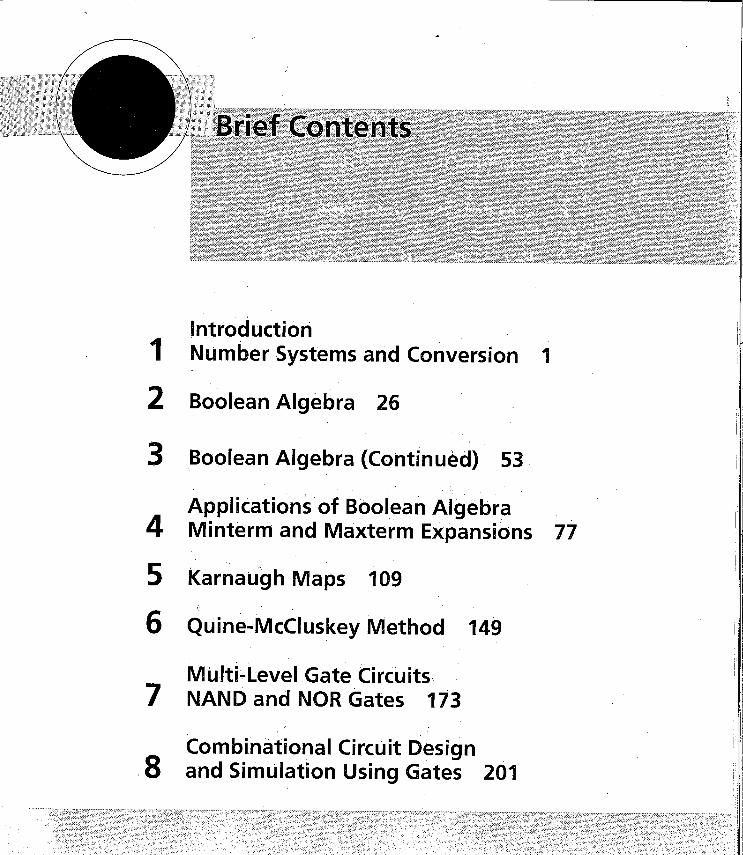
Introduction 1 Number Systems and Conversion 1
2 Boolean Algebra 26
3 Boolean Algebra (Continued) 53
Applications of Boolean Algebra 4 Minterm and Maxterm Expansions 77
5 Karnaugh Maps 109
6 Quine-McCluskey Method 149
Multi-Level Gate Circuits 7 NAND and NOR Gates 173
Combinational Circuit Design 8 and Simulation Using Gates 201
viii Brief Contents
Multiplexers, Decoders, and Programmable
9 Log ic Devices 224
10 Introduction to VHDL 257
11 Latches and Flip-Flops 290
12 Registers and Counters 319
13 Analysis of Clocked Sequential Circuits 355
14 Derivation of State Graphs and Tables 390'
Reduction of State Tables 15 State Assignment 425
'16 Sequential Circuit Design 465
17 VHDL for Sequential Logic 501
18 Circuits for Arithmetic Operations 535
19 State Machine Design with SM Charts 563
20 VHDL for Digital System Design 583
A Appendices 610
Preface xix How to Use This Book for Self-Study xxiii
Introduction 1 Number Systems and Conversion 1
••••••••••••••••••••••••••••••••••••••••••••••••••• Objectives 1 Study Guide 2
1.1 Digital Systems and Switching Circuits . 6 1.2 Number Systems and Conversion 8 1.3 Binary Arithmetic 12 1.4 Representation of Negative Numbers 15
Addition of 2's Complement Numbers 17 Addition of l' s Complement Numbers 18
1.5 Binary Codes 20 Problems 23
2 Boolean Algebra 26 •••••••••••••••••••••••••••••••••••••••••••••••••••
Objectives 26 Study Guide 27
2.1 Introduction 33
X Contents
2.2 Basic Operations 34 2.3 Boolean Expressions and Truth Tables 36 2.4 Basic Theorems 38 2.5 Commutative, Associative, and Distributive Laws 39 2.6 Simplification Theorems 41 2.7 Multiplying Out and Factoring 43 2.8 DeMorgan's Laws 45
Problems 47 Laws and Theorems of Boolean Algebra 52
3 Boolean Algebra (Continued) 53 . . . . . . . . . . '. . . . . . . . . . . . . . . . . . . . . . . . . . . . . . . . . . . . . . . . .
4
Objectives 53 ~tudy Guide 54
3.1 Multiplying Out and Factoring Expressions 58 3.2 Exclusive-OR and Equivalence Operations 60 3.3 The Consensus Theorem 62 3.4 Algebraic Simplification of Switching Expressions 64 3.5 Proving the Validity of an Equation 66
Programmed Exercises 68 Problems 74
Applications Qf Boolean Algebra Minterm and Maxterm Expansions 77
" ••••••••••••••••••••••••••••••••••••••••••••••••••• Objectives 77 Study Guide 78
4.1 Conversion of English Sentences to Boolean Equations 84 4.2 Combinational Logic Design Using a Tr:uth Table 86 4.3 Minterm and Maxterm Expansions -87 4.4 General Minterm and Maxterm Expansions 90 4.5 Incompletely 'Specified Functions 93 4.6 Examples of Truth Table Construction 94 4.7 Design of Binary Adders and Subtracters 98
Problems 101
; , ,
Contents xi
5 Karnaugh Maps 109 • ••••••••••••••••••••••••••••••••••••••••••••••••••
Objectives 109 Study Guide 110
5.1 Minimum Forms of Switching Functions 120 5.2 Two- and Three-Variable Karnaugh Maps 121 5.3 Four-Variable Karnaugh Maps 126 5.4 Determination of Minimum Expressions
Using Essential Prime Implicants 129 5.5 Five-Variable Karnaugh Maps l34 5.6 Other Uses of Karnaugh Maps l36 5.7 Other Forms of Karnaugh Maps 138
Programmed Exercises l39 Problems 144
6 Quine-McCluskey Method 149 • ••••••••••••••••••••••••••••••••••••••••••••••••••
Objectives 149 Study Guide 150
6.1 Determination of Prime Implicants 155 6.2 The Prime Implicant Chart 158 6.3 Petrick's Method 161 6.4 Simplification of Incompletely Specified Functions 162 6.5 Simplification Using Map-Entered Variables 163 6.6 Conclusion 165
Programmed Exercise 166 Problems 170
Multi-Level Gate Circuits 7 NAND and NOR Gates 173
• •••••••••••••••••••••••••••••••••••••••••••••••••• Objectives 173 Study Guide 174
7.1 Multi-Level Gate Circuits 179 7.2 NAND and NOR Gates 183
xii Contents
8
7.3 Design of Two-Level Circuits Using NAND and NOR Gates 185 -7.4 Design of Multi-Level NAND and NOR Gate Circuits 188 7.5 Circuit Conversion Using Alternative Gate Symbols 189 7.6 Design of Two-Level, Multiple-Output Circuits 192
Determination of Essential Prime Implicants for Multiple-Output Realization 194
7.7 Multiple-Output NAND and NOR Circuits 196 Problems 196
Combinational Circuit Design and Simulation Using Gates 201
•••••••••••••••••••••••••••••••••••••••••••••••••••
9
Objectives 201 Study Guide 202
8.1 Review of Combinational Circuit Design 205 8.2 Design of Circuits with Limited Gate Fan-In 206 8.3 Gate Delays and Timing Diagrams 208 8.4 Hazards in Combinational Logic 210 8.5 Simulation and Testing of Logic Circuits 213
Problems 216 Design Problems 218
Multiplexers, Decoders, and Programmable log ic Devices 224
••••••••••••••••••••••••••••••••••••••••••••••••••• Objectives 224 Study Guide 225
9.1 Introduction 230 9.2 Multiplexers 230 9.3 Three-State Buffers 233 9.4 Decoders and Encoders 235 9.5 Read-Only Memories 238 9.6 Programmable Logic Devices 242
Programmable Logic Arrays 242 Programmable Array Logic 245
9.7 Complex Programmable Logic Devices 247
9.8 Field Programmable Gate Arrays 249 Decomposition of Switching Functions 250 Problems 253
10 Introduction to VHDl 257
Contents xiii
••••••••••••••••••••••••••••••••••••••••••••••••••• Objectives 257 Study Guide 258
10.1 VHDL Description of Combinational Circuits 262 10.2 VHDL Models for Multiplexers 265 10.3 VHDL Modules 267
Four-Bit Full Adder 269 10.4 Signals and Constants 272 10.5 Arrays 273 10.6 VHDL Operators 276 10.7 Packages and Libraries 277 10.8 IEEE Standard Logic 279 10.9 Compilation and Simulation ofVHDL Code 282
Problems 283
11 latches and Flip-Flops 290 •••••••••••••••••••••••••••••••••••••••••••••••••••
Objectives 290 Study Guide 291
11.1 Introduction 295 11.2 Set-Reset Latch 296 11.3 Gated D Latch 300 11.4 Edge-Triggered D Flip-Flop 301 11.5 S-R Flip-Flop 303 11.6 J-KFlip-Flop 305 11.7 T Flip-Flop 306 11.8 Flip-Flops with Additional Inputs 307 11.9 Summary 309
Problems 310 Programmed Exercise 316
r:
xiv Contents
Registers and Counters 319 • ••••••••••••••••••••••••••••••••••••••••••••••••••
Objectives 319 Study Guide 320
12.1 Registers and Register Transfers 325 Parallel Adder with Accumulator 327
12.2 Shift Registers 329 12.3 Design of Binary Counters 333 12.4 Counters for Other Sequences 338
Counter Design Using D Flip-Flops 341 12.5 Counter Design Using S-R and J-K Flip-Flops 342 12.6 Derivation of Flip-Flop Input Equations-Summary 345
Problems 349
13 Analysis of Clocked Sequential Circuits 355 • ••••••••••••••••••••••••••••••••••••••••••••••••••
Objectives 355 Study Guide 356
13.1 A Sequential Parity Checker 362 13.2 Analysis by Signal Tracing and Timing Charts 364 13.3 State Tables and Graphs 367
Construction and Interpretation of Timing Charts 372 13.4 General Models for Sequential Circuits 374
Programmed Exercise 378 Problems 382
14 Derivation of State Graphs and Tables 390 • ••••••••••••••••••••••••••••••••••••••••••••••••••
Objectives 390 Study Guide 391
14.1 Design of a Sequence Detector 393 14.2 More Complex Design Problems 398 14.3 Guidelines for Construction of State Graphs 402 14.4 Serial Data Code Conversion 407
I 'I
!
I ,
ps
15
14.5 Alphanumeric State Graph Notation 410 Programmed Exercises 412 Problems 419
Reduction of State Tables State Assignment 425.
. ,
Contents xv
••••••••••••••••••••••••••••••••••••••••••••••••••• Objectives 425 Study Guide 426
15.1 Elimination of Redundant States 433 15.2 Equivalent States 434 15.3 Determination of State Equivalence Using an Implication Table 437 15.4 Equivalent Sequential Circuits 440 15.5 Incompletely Specified State Tables 442 15.6 Derivation of Flip-Flop !nputEquations 443 15.7 Equivalent State Assignments ·446 15.8 Guidelines for State Assignment 449 15.9 Using a One-Hot State Assignment 453
Problems 455
16 Sequential Circuit Design 465 •••••••••••••••••••••••••••••••••••••••••••••••••••
Objectives 465 Study Guide 466
1 ~.1 Summary of Design Procedure for Sequential Circuits 468 16.2 Design Exampl~-Code Converter 469 16.3 Design of Iterative Circuits· 472
Design of a Comparator 473 16.4 Design of Sequential Circuits Using ROMs and PLAs 476 16.5 Sequential Circuit ])esign Using CPLDs 479 16.6 Seqmmtial Circuit Design Using FPGAs 483 16.7 Simulation and Testing of Sequential Circuits 485 16.~ Overview of Compllter-Aided Design 490
Design Problems . 492 Additional Problems 498
xvi Contents
17 VHDL for Sequential Logic 501 •••••••••••••••••••••••••••••••••••••••••••• •••••••
Objectives 501 Study Guide 502
17.1 Modeling Flip-Flops Using VHDL Processes 506 17.2 Modeling Registers and Counters Using VHDL Processes 509 17.3 Modeling Combinational Logic Using VHDL Processes 514 17.4 Modeling a Sequential Machine 515 17.5 Synthesis ofVHDL Code 522 17.6 More about Processes and Sequential Statements 525
Problems 527 Simulation Problems 533
18 Circuits for Arithmetic Operations 535 •••••••••••••••••••••••••••••••••••••••••••••••••••
Objectives 535 Study Guide 536
18.1 Serial Adder with Accumulator 538 18.2 Design of a Parallel Multiplier 542 18.3 Design of a Binary Divider 546
Programmed Exercises 551 Problems 555
19 . State Machine Design with SM Charts 563 •••••••••••••••••••••••••••••••••••••••••••••••••••
Objectives 563 Study Guide 564
19.1 State Machine Charts 565 19.2 Derivation of SM Charts 569 19.3 Realization of SM Charts 575
Problems 579
-Contents xvii
20 VHDL for Digital System Design 583 •••••••••••••••••••••••••••••••••••••••••••••••••••
Objectives 583 Study Guide 584
20.1 VHDL Code for a Serial Adder 587 20.2 VHDL Code for a Binary Multiplier 588 20.3 VHDL Code for a Binary Divider 599 20.4 VHDL Code for a Dice Game Simulator 601 20.5 Concluding Remarks 604
Problems 605 Lab Design Problems 608
A Appendices 610 •.•......••..•...•...........••....••..•..........•.......••........••...•......••.••..........••..•..
A MOS and CMOS Logic 610 B VHDL Language Summary 616 C Proofs of Theorems 621
References 623
Answers to Selected Study Guide Questions and Problems 624
Index 681
74163,511 74178,351 Accumulator
parallel,327-329 serial, 538-541
Active low, 307 Adder, binary, 95-96
parallel, 98-99 parallel with accumulator, 327-329, 482, 485 serial, 370-372 serial with accumulator, 538-541 VHDL serial adder, 587-588
Addition, binary, 12 one's complement, 18-20 two's complement, 17-18
Algebraic simplification, 41-43,64-66, 120-121
Algorithmic state machine. See State machine. Alphanumeric state graph notation, 410-412 Alternative gate symbols, 189-192 Analog systems, 6 AND
logic gate, 34 VHDL,265
Arithmetic, binary. See Addition, binary and Subtraction, binary.
ASCII code, 21-22, 240-241 ASIC, 491
ASM chart. See SM chart. Associative law, 39-40 Asynchronous sequential circuit, 309
Base conversion, 8-12 Bi-directional I/O Pin, 235
VHDL,281 Binary addition. See Addition, binary. Binary numbers
conversion to decimal, 8-10 signed, 15-17
Binary subtraction. See Subtraction, binary. Binary-coded-decimal (BCD), 20 BITLIB, 278, 619 Boolean algebra, 33-47, 58-68
basic operations, 34-36 basic theorems, 38-39 laws and theorems, 52 simplification theorems, 41-43
Boolean expressions, 36-37 Borrow, 12-14, 17-20 Buffer, 233-35 Bus, 232
Carry, 12 end-around,18-20 flip-flop, 98-99
Characteristic equations, 309
682 Index
Clear input asynchronous, 307-308 synchronous, 512
Clocked sequential circuit. See Sequential circuit, synchronous.
CMOS Logic, 611-613 Code converter
ASCII, 240-241 sequential, 469-472 sequential in VHDL, 515-516
Codes (BCD, 8-4-2-1, 6-3-1-1, excess-3, Gray, 2-outof-5, weighted), 20-22
Combinational circuit definition, 7 design, 86-87,205-206 testing, 213-215
Commutative law, 39 Comparator, 473-476
VHDL,276 Complementation, 34. See also Inversion. Computer-aided design (CAD), 248, 490-492 Configurable logic block (CLB), 249-250
Xilinx Spartan, 604 Xilinx Virtex / Spartan II, 483-484
Consensus theorem, 62-64 dual, 63 illustrated by map, 125
Contact bounce, 299 Control circuit
for dice game, 572 for divider, 546-551 for multiplier, 542-545 for serial adder, 538-541
Conversion of circuits, 189-192 Converting English sentences to Boolean equations,
84-85 Counters, 333-345
binary, 333-338 design using D flip-flops, 341-342 design using J-K flip-flops, 343-346 design using S-R flip-flops, 342-343 fully synchronous, 511 up-down, 335-337 VHDL,511
CPLD, 479-483, 283, 479-480 sequential circuit design using, 479-483
Cyclic shift register VHDL,509
D (delay) flip-flop, 301-303 CMOS,615 derivation of input equations, 444 modeling in VHDL, 506 with clock enable, 308
Data selector. See Multiplexer. Debouncing switches, 299 Decimal numbers
binary codes for, 21 conversion to binary, 8-12
Decoder, 235-237 Decomposition of switching functions, 250-252 Degenerate forms, 187 DeMorgan's laws, 45-47 Dice game, 571-575
VHDL,601-603 Digital systems, 6-8
design with FPGA, 483-485 Distributive law, 41 Divider, parallel binary, 546-551, 570
VHDL,599-601 Division
binary, 15,546-551 Don't care term, 93
in Karnaugh map, 127 in prime implicant chart, 162-163
Dual, 47
EEPROM,240 Encoder, 237-238 Equation
proving validity, 66-68 Equivalence gate, 61-62 Equivalent sequential circuits, 440-441
by implication table, 440-441 definition, 440 determination of, 440
Equivalent states, 434-436 definition, 436 in SM chart, 575 theorem, 436
Espresso-II method, 166 Essential prime implicant
definition, 131, 159 from Kamaugh map, 130-133 from prime implicant chart, 158-160 mUltiple output, 194-195 proof,621
Exclusive-OR,60-61 Expansion theorem, 250-251
Factoring, 44-45, 59 False output, 366-367, 373-374 Fan-in, 206
reduction of, 206-208 Flip-flop
characteristic equation, 309 clear, preset inputs, 307-308 D,301-303 D-CE,308 definition, 295 J-K, 305-306 master-slave, 304 modeling using VHDL, 506-509 S-R, 303-305 T,306-307 type conversion, 307
Flip-flop input equations, derivation D,335,341,444,452-453 J-K,343-346,443-445 S-R, 342-343, 445 summary, 345-348,443 T,333-334,338-341
Flowchart, 565 FPGA, 249-250, 483-484
sequential circuit design using, 485 FPLA,245 . Full adder, 98
implemented using a PAL, 247 VHDL, 269-:,472
Full subtracter, 100-101 Function block, 247 Function generator, 250 Functionally complete, 184
Gate circuits, 45 2-level NAND and NOR, 185-188 multi-level, 179-183, 188-189 multiple-output, 192-196,206-208
Gate delays, 180, 208-210 Gate level, 179-183
Gates AND,34 equivalence, 61-62 exclusive-or, 60 NAND. See NAND gate. NOR. See NOR gate. OR,35 transmission, '613
Glitches, 408
Index 683
Hardware description languages (HDLs), 248, 49l. See also VHDL.
Hazards, 210-213 Hexadecimal number, 9, 11 Hold time, 302-303
IEEE standard logic, 279-282, 520 Implicant
definition, 129, 157 Implication table, 437-440 Incompletely specified function, 93-94
simplification, 127, 162-163 Incompletely specified sequential circuits, 442-443 Integrated circuits
design and layout, 491 in combinational circuit design, 213, 230-250 in sequential circuit design, 486 MOS, CMOS, 610-615 SSI, MSI, LSI, VLSI, 230 TTL,511
Interconnect array (IA), 247 Inversion, 45-47. See also Complementation. Inverter, 34, 189, 611, 612 Iterative circuits, 472-476
definition, 472 design, 472-476
J-K flip-flop, 305-306 derivation of input equations, 343-346 master-slave, 306 VHDL,508-509
Kamaugh map, 120-137 3-variable, 121-126
i !
684 Index
4-variable, 126-128 5-variable, 134--136 complementation, 125 multiple-output minimization, 192-195 otherforms, 138
Laboratory testing combinational circuits, 213-215 sequential circuits, 485-490
Latch CMOS, 614-615 definition, 295 GatedD,300 S-R, 296-300 unwanted in VHDL processes, 524
Left shift register VHDL,51O
_ Link path, 566, 576 Literal
definition, 36 elimination of, 65
LogicPUd, 117, 119, 153,204,392,490,578 Lookup table (LUT), 249, 483 Looping terms on a Karnaugh map,
122-124
Macrocell,479-83 Xilinx CoolRunner, 604
Manchester code, 408-410 Map-entered variables, 163-165,579 Maxterm
definition, 88 Maxterm expansion, 87-90
general, 90-93 simplification of, 121
Mealy sequential circuit, 364, 369 Metal-oxide semiconductor. See MOS. Microsecond, 209 Minimum product of sums, 121
from Karnaugh map, 128 Minimum sum of products, 120
from Karnaugh map, 124, 129 from prime implicant chart, 158-160
Min-max delay, 486 Minterm
definition, 87
Minterm expansion, 87-90 general, 90-93 simplification of, 120
Moore sequential circuit, 364 general model, 374-375, 376
MOS logic, 610-615 MOSFET,61O Multi-level gate circuits
design, 179-183 NAND and NOR gates, 188-189, 192-196
Multiple-output gate circuit design, 192-195,206-208 determination of essential prime implicants, 194--195
Multiplexer (MUX), 230-232 data selection, 232 VHDL, 265-267
Multiplication, binary, 14,542-545 Multiplier, parallel binary, 542-545, 570-571,
576-577 VHDL, 588-599
Multiplying out, 43, 58-60
NAND gate, 183 2-level circuits, 185-188 CMOS, 613 functionally complete, 184 multi-level circuits, 188-189
Nanosecond,208 Negative logic, 508, 611 Negative number representation, 15-17. See also
One's complement, Two's complement. sign and magnitude, 15
Next state, 298 map, 338
Nominal delay, 486, 488 NOR gate, 184
2-level circuits, 185-188 CMOS, 613 multi-level circuits, 188-189
NOT gate. See Inverter. ~,~Icodes,407-408
Number systems, 8-12
One's complement addition; 18-20 representation of negative number, 15-17
I I' 11
One-hot state assignment, 453 OR gate, 35 Overflow
division, 547 one's complement addition, 18-20 two's complement addition, 17-18
PAL, 245-247 in sequential circuit design, 479
Parallel adder, 99 Parity, 362 Parity checker , sequential, 362-364
PC board layout, 491 Petrick's method, IH-162 Phase-locked. loop, 407 PLA,242-245
in sequential circuit design, 476-479, 576-578
table, 243 PLD
bit pattern generation, 490 programmer, 499
Positive logic; 610 ' Present state, 298 Prime implicant. See also Essential prime
implicant: chart, 158-160, definition, 129, 158 from Karnaugh map, 129-130
Product of sums, 44 stand.ard, 88
PrograrnJJ:].able array logic. See PAL. Programmable logic array. See PLA. Programmable i9giC device, 242-247 PROM
compared with PLA, 245 programmer, 241
Proofs of theorems, 621-22 Propagation delay, 208
Quine-McCluskey method, 154-163
Redundant states, elirlnnation of, 433-434 Register transfers, 325~327 Registers, 324-,333
Index 685
ROM (read-only memory), 238-242 in sequential ciTcuit design, 476-479, 578 VHDL,275 '
RZ code, 408
Schematic capture, 490 Sequence detector design, 393-402 Sequential circuit
definition, 7 ~equential circuit, synchronous. See also State graph,
State machine, State table, Mealy sequential circuit, Moore sequential circuit, ~tate assignment .•
analysis, 361-377 design with a PAL, 479 design with flip-flops, 468-472 design with PLA, 476-479 design with ~OM, 476-479 general model; 374-377 testing, 485-490 timing charts, 364-367
Serial adder. See Adder, serial. Serial data "
code conver~ion, 407-410 transmissio~of, 407-408
Set-Reset (S-R) flip-flop, 303-305 derivation of input equations, 342-343, 445
Setup time, 376 Seven-segment indicator, 218 Shift register, 329-333
cyclic, 329 Sign and magnitude, 15 Signal tracing, ~64 Simplification. ~ee Algebraic simplification. SimUaid, 291, ~51, 490-491 Simulation
logic circuits, 213-215 , sequential circuits, 485-490
SM block, 565 ' , SM chart (~tate machine chart), 565-579 derivation,569~575 for binary divider, 570
, for binary multiplier, 570-571 , for dice game, 571-575 realization, 575-579
Stabl~ state, 296
686 Index
Standard product of sums, 88
Standard sum of products, 87
State assignment for synchronous circuits, 446-455
equivalent assignments, 446-449
guidelines, 449-453 one hot, 453-455
State equivalence theorem, 436, 621-622
State graph alphanumeric notation, 410-412
conversion to SM chart, 568-569
derivation, 393-407 for control circuits, 538-541, 542-545, 546-549
for counter, 338, 341 guidelines for construction, 402-407
Mealy, 369-370 Moore,369
State machine, 398, 517, 520. See also Sequential
circuit, synchronous.
design using SM charts, 565-579
State table reduction, 433-440
State table derivation, 393-407
incompletely specified, 442-443
Mealy, 369-370 Moore,368
Subtracter full, 100-101 in binary divider, 548-551
Sum of products, 43 standard, 87
Switches circuits of, 35-36, 38-39
Switching algebra, 33. See Boolean algebra.
Switching circuit definition, 7
Switching function decomposition of, 250-252
Synchronizer, 490 Synchronous sequential network. See Sequential
network, synchronous.
T (toggle) flip-flop, 306-307
derivation of input equations, 333-334, 338-341
Test generation, 491 Testing of circuits. See Laboratory testing.
Three-state buffer. See Tri-state buffer.
Timing diagram, 208-210
for counter, 340-341 for flip-flops, 297-298, 301, 304
for sequential circuits, 367, 364-367, 372-374
for SM chart, 568-569
Transients in output, 210
Transition table, 368 Transmission gate (TG), 613
Tri-state buffer, 233-235
VHDL, 279, 281 Tri-state logic, bus, 233-235
Truth table, 37 construction, 94-97
TTL logic, 511 Two's complement
addition, 17-18 representation of negative number, 15-17
Unwanted latches in VHDL, 524
Veitch diagram, 138 Verilog HDL, 261, 491
VHDL arrays, 273-275 case-sensitivity in, 264 compilation, 282 concurrent statements, 263, 507, 514, 604
data types, 273, 279 definition, 261 delta time, 263, 283, 525
evaluation and execution of statements, 262-264
introduction to, 261-283
language summary, 616-618
latches (unwanted), 524
libraries, 278-279, 618-620
module, 267 operators, 276-277 overloaded openltors, 280, 511
packages, 278, 618-620
process, 506-507, 525-526
sequential statements, 506, 507, 592
signals, 262, 264, 267 signals, change of value, 524
signals, external, 516 .
signals, internal, 592
~'
1 1
simulation, 282-283 std_logic, 279, 280, 619, 620 synthesis, 283, 522-525, 605 test bench, 591-593 type conversion, 620 unsigned type, 619
VHDL models for bi-directional 110 pin, 281 for binary divider, 599-601 for binary multiplier, 588-599 for code converter, 515-516 for combinational logic, 514-515 for comparator, 276 for counter, 511 for cyclic shift register, 509 for dice game simulator, 601--603 for flip-flops and latches, 506-509 for full adder, 272 for gates, 262-265 for left shift register, 510 for multiplexer, 265-267 for ROM, 275 for sequential logic, 506-527 for sequential machine, 517-521 for serial adder, 587-588 for tri-state buffer, 279, 281
VHDL statement alias declaration, 590, 617 architecture declaration, 267, 268, 616 array type and object declaration, 274, 617
Index 687
case, 515, 618 component declaration, 269, 271, 617 component instantiation, 272, 617 conditional signal assignment, 265, 266, 617 constant declaration, 272, 616 entity declaration, 267, 268, 616 for loop, 592, 618 if-then-else, 507, 618 integer type declaration, 272, 616 interface-signal declaration, 616 library declaration, 278, 618 package body, 277, 619 package declaration, 277, 619 port declaration, 267, 268 process with sensitivity list, 506-507, 617 process without sensitivity list, 525, 618 report declaration, 618 selected signal assignment, 266-267, 617 signal assignment statement, 262-263, 617 signal declaration, 272, 616 use, 278, 619 wait, 525, 618
Word problems, 84-85, 94-97
Xilinx CoolRunner CPLDs, 479-483, 479, 604 Xilinx Spartan, 483-484, 604 Xilinx VirtexlSpartan II, 483-484, 604