Charge and Exciton Dynamics in Organic Optoelectronic Devices

Charge Transport in Disordered Organic Materials andIts Relevance to Thin-Film Devices: A Tutorial Review
By Nir Tessler,* Yevgeni Preezant, Noam Rappaport, and Yohai Roichman
1. General Introduction
In this review, we describe a variety of models or theoreticalapproaches to transport in disordered media and discuss theimplication to modern organic devices. There are far too manymodels or variations, so our aim is not to try to cover them all.Instead, we show that when the different models are presentedalong with the assumptions included while being developed, theycan all teach us and help us to develop some intuition regardingwhat goes on in nonordered materials. One may encounterdebates regarding a model being wrong, but it is our belief thatonly when the models are used out of context (not within theirbasic assumptions) the obtained results could be false.
One of the things one encounters while starting to studyorganic semiconductors is that the textbook models taught insemiconductor-device courses have to be revisited, and one has tolook for ‘‘old’’ books that were written before silicon technologytook over. With this spirit, we start a few years back, or a centuryago. In 1900, three years after the discovery of the electron byThomson, Drude proposed a model that explained the knownconductivity phenomenon in metals and other types ofmaterials.[1] This model was based on the assumption thatelectrons classically accelerate under an applied electric field andcollide with the lattice’s heavy positive ions. Upon collision, theelectrons were assumed to scatter into a random angle and at aspeed that was on average consistent with the local temperature.It would then go on accelerating until the next scattering event.This model, although erroneous in the assumption that the basicscattering centers were the lattice ions, was able to physically
explain the already known Ohm’s law andthe Joule heating effect. Along with thedebut of quantum mechanics came thequantum mechanical description of matterand the realization that in a well-orderedlattice electrons should be mathematicallydescribed as Bloch waves, and that thescattering was not the result of collisionswith any lattice ion but rather scatteringfrom defects, contaminations, and pho-nons. Nevertheless, the Drude model,under the semiclassical approximation, is
conceptually appropriate for describing electron transportthrough crystal lattices, that is, freely roaming charge carriersthat scatter upon collisions with defects, contaminations, andphonons. The carriers earn the name ‘‘free’’ whenever thematerial properties are such that the mean free path betweencollisions, L, is much longer than the typical carrier’s Blochwavelength, thus the carriers have very broad wavefunctionsextending over many lattice units.
However, as was historically elucidated by Anderson,[2]
introducing disorder into the lattice and breaking the crystalsymmetry results in the wavefunctions becoming localized and inthe formation of energy states in the forbidden band-gap. TheDrude concepts, and others deriving on its intuitive approach, canno longer serve us in explaining transport under suchcircumstances. Since the materials we are interested in aredisordered in nature, we shall devote the discussion to somephenomena and physical theories relating to the transport ofcharge carriers through disordered media. As stated at thebeginning, we do not aim to cover all existing theories orvariations, but rather discuss only those that would help indeveloping some intuitive understanding of the transport inamorphous organic materials.
The discussion in the following section starts in an abstractmode, so to help the reader place it in the right context we outline,briefly, how one could represent a film of conjugated polymers (ormolecules) by a map of sites a charge would go through whiledrifting with the electric field. Figure 1a shows schematically adistribution of conjugated polymer chains as might be found in asmall section of a polymer film. It is well known that theconjugated polymer is not a single electronic wire but that it israther broken into subunits (by chemical or physical defects) thatare called conjugation units, and the number of monomersmaking this unit is called the conjugation length. Figure 1b showshow the polymer chains would be broken into subconjugationunits. Namely, we have now many small electronic units that canalso be thought of as small molecules distributed across the film.The ‘‘only’’ role that was played by the polymer chain was to
REVIE
W
www.advmat.de
[*] Prof. N. Tessler, Y. Preezant, Dr. N. Rappaport, Dr. Y. RoichmanElectrical Engineering DepartmentNanoelectronic CenterTechnion, Haifa 32000 (Israel)E-mail: [email protected]
DOI: 10.1002/adma.200803541
Semiconducting polymers and small molecules form an extremely flexibleclass of amorphousmaterials that can be used in a wide range of applications,some of which are display, radio-frequency tags, and solar cells. The rapidprogress towards functional devices is occurring despite the lack of sufficientunderstanding of the physical processes and very little experience in deviceengineering. This tutorial review aims to provide sufficient intuitive back-ground to draw more researchers to look into the fundamental aspects ofdevice physics and engineering.
Adv. Mater. 2009, 21, 2741–2761 ! 2009 WILEY-VCH Verlag GmbH & Co. KGaA, Weinheim 2741

REVIE
W
www.advmat.de
determine the distribution of the units (‘‘molecules’’) in the filmthat is part of the film morphology.
Having simplified the film into an ensemble of electronic sites,we can ‘‘forget’’ that we had polymers or molecules and considerthat we have a distribution of sites that can host charge and enableit to move across a film. As Figure 2 shows, we need now toanalyze charge transport across sites that are distributed in realspace (Fig. 2a) as well as in energy space (Fig. 2b). The solid line inFigure 2 illustrates an imaginary path a charge might take whilecrossing the film.
2. Charge Motion in Disordered OrganicMaterials
As we have already mentioned, in well-ordered materialstransport is essentially modeled by application of the semi-classical approximation and the Drude model. There exists asimple exception to this picture, where the role of trap states inthe forbidden gap is included. In that case, the transport isessentially ideal, that is, only that at a given time a certainpercentage of the carriers are considered to be trapped inlocalized states, and are therefore static and not contributing tothe current.[3] This changes the relation between the voltage andthe current, but does not change the concept of how the carriersare transported. The conceptual leap in understanding transportin disordered media is in realizing that current can also be theresult of charge transport through localized states.
Three essential depictions are given in Figure 3 for the nature ofthe relevant states in the material. The filled areas in the figuresignify that the states are localized. In Figure 3a the localized statesare shown to reside in the forbidden band-gap between the freecarrier bands. This scenario is similar to what has beenmentionedabove, where depending on the relative position of the traps andtheir density they may be deep or shallow. Figure 3b shows ascenario where the trap states comprise the lower part of the wholeconduction band with an energy EM (the mobility edge), beyondwhich the states are unlocalized. This is more like a shallow-trapsituation. In Figure 3c the entire band is comprised of localizedstates. Under the first two circumstances, the current will mostlikely (although not necessarily) be dominated by the unlocalizedcarriers; however, in the third case that cannot be true.
One may suppose that if all carriers occupy states that arelocalized, then the material should invariably be considered aninsulator.However, localized charge carriersmay travel through thematerial by hopping from one localized state to the next. The rate atwhich thisoccurs is related to theconductivityof thematerial, and insome cases also to the concept of mobility. A carrier may hop fromonesite to thenext provided the site of origin is occupiedbya carrierand the target site can accept additional carrier (typically thismeansthat the target site is unoccupied). Therefore, in order to describethis process, a probability evolution equation is needed, known asthe master equation:
@
@tfi!t" # $
X
j 6#i
Wjif !t"%1$ fi!t"&
'X
j 6#i
Wijfj !t"%1$ fi!t"&
$ lifi!t" (1)
In Equation 1 fi(t) is the probability that site i(at location Ri and energy ei) is occupied by acarrier or excitation at time t (therefore%1$ fj!t"& is the probability that site j isunoccupied), Wij is the transition rate fromsite i to site j, and li is the decay rate of the
Nir Tessler received his B.Sc.summa cum laude in ElectricalEngineering at Technion IsraelInstitute of Technology. After‘‘falling in love’’ with organicoptoelectronics he strived tocontribute to the understand-ing that organics can be usedin numerous applicationswhere the latest example wasof polymer based LEDs emit-ting at telecom wavelengths. In1999, he joined the Technion
as a faculty member studying new materials, device designand analysis, and charge transport and related phenomena indisordered amorphous materials based devices.
Figure 1. a) Schematic description of polymer chains. b) Illustration ofhow a long chain would break into small conjugation units (or sites).
Figure 2. Schematic description showing that the transport sites are distributed both a) in spaceand b) in energy. c) A schematic 2D map of a rough energy surface. The line describes ahypothetical path a charge might take while hopping from one side of the sample to the other(under applied electric field).
2742 ! 2009 WILEY-VCH Verlag GmbH & Co. KGaA, Weinheim Adv. Mater. 2009, 21, 2741–2761

REVIE
W
www.advmat.de
excitation at site i. This is a nonlinear equation with a potentiallyextremely large number of terms. For a given problem, the sitelocations {Ri} need be given as well as the decay rates for each site(often one assumes that recombination is only a smallperturbation, and assumes that li# 0). Two popular expressionsfor the Wij transition rates were given by Anderson (what isknown in the organic semiconductor field as the Miller–Abrahams expression) and by Mott.[4] The Miller–Abrahamsexpression[5,6] is based on a phonon-assisted tunneling mechan-ism, and is given by:
Wij # y0exp!$2gjRijj" exp $!"j $ "i"
kT
! "8"j > "i
1 else
8<
: (2)
where y0 is the phonon vibration frequency (can be intuitivelyunderstood as the ‘‘jump-attempt’’ rate or simply taken as anormalization factor), g is the inverse localization radius (theresult of the overlap integral of the wavefunctions assumingexponential decay with distance), and ei and ej are the energylevels of the respective sites. In this model, no relaxation of thelocal site configurations (the polaronic effect) is accounted for.The second popular approach for expressing the transfer rate isbased on the polaronic effect, which describes the couplingbetween the molecule configuration (physical structure) and itselectronic energy. In this case, the (two) molecules involved in thecharge transfer (or chemical reaction) should first assume aconfiguration in which the total energy is indifferent to the chargebeing on one molecule or the other. In some sense, one may saythat the charge transfer would occur when the molecular statesinvolved are at resonance. Namely, charge carrier may hop fromone site to another given that a favorable configuration is reached(the chances for which are temperature dependent). The resultingexpression from this analysis is:[4]
Wij #J2
!hp##############
2UbkTp exp $ Ub
2kT
! "
exp $!"j $ "i"2kT
$b!"j $ "i"2
8kTUb
! (3)
where J is related to the overlap integral and is given byJ2 # J20exp! $ 2gjRijj" with J0 calculated from the crossing point
between the reactant and product curves[7] andUb is the polaron binding energy.
Although the energy dependence of thetransfer rate is very different between theMiller–Abraham’s (M.A.) and the polaronic one(see Fig. 4), under steady-state and qua-si-equilibrium (low E field) conditions thereis no real difference between the transport(current) derived from Equations 2 and 3, butfor the additional activation energy associatedwith the polaron binding energy. There ishowever, an inherent difference, relevant tosteady-state conditions, which does not appear
in these equations and has to do with the fact that the mostfavorable configuration at which charge transfer occurs is one thatcan be accessed through the phonons (vibration types) present inthe system (in the solid, the relevant vibrations are both intra- andintermolecular). As the temperature goes down, the relativeoccupation of different vibration changes, and at sometemperature ((half of the significant ‘‘phonon temperature’’)the ‘‘high-temperature favorable configuration’’ cannot bereached through the existing vibrations, and a new ‘‘low-temperature favorable configuration’’ is chosen. For this newconfiguration, the tunneling is much slower, but as it requiresless energy to be reached, it is associated with lower activationenergy. We have not been able to find direct measurements of thephonon temperature associated with the charge transport, but theone associated with exciton emission in conjugated polymers is inthe range of 300–500K.[8,9] Namely, in most temperature-dependent measurements this effect will be highly influential,andmaymask the effects that are dominant in hardmaterials. Wewill come back to the issue of polaronic transfer rate in the contextof nonequilibrium transport further ahead in this paper.
Regardless of the transfer rate of choice, one has to find asolution for Equation 1. There are several approaches to handlingthis equation in order to arrive at useful results. In many cases,this requires the linearization of Equation 1 by either assuming adilute system (low density) of uncorrelated particles, and thuseliminating the terms [1$ fi(t)] and/or by assuming smalldeviations from equilibrium, and thus the overall rates are linear
Figure 3. Different scenarios for the setting of traps in relation to the general density of states—a) in the forbidden band-gap isolated from the main bands, b) edge portion of one of the bandswith a typical mobility edge energy (EM) beyond which the states are free, c) and a completelylocalized band.
Figure 4. The transfer rate as a function of the energy difference betweeninitial and final states (negative# going down in energy) for the Mill-er–Abraham’s and polaronic rates (shown for binding energies of 0.05 and0.3 eV).
Adv. Mater. 2009, 21, 2741–2761 ! 2009 WILEY-VCH Verlag GmbH & Co. KGaA, Weinheim 2743
REVIE
W
www.advmat.de
with the difference in electrochemical potential (quasi-Fermilevel). Next, in Section 3, we briefly outline some semi-phenomenological models that are based on the basic equationsabove. This will be followed in Section 4 with more computer-intensive models.
2.1. Behind the Scenes
Throughout the paper we will try to draw you attention to‘‘hidden’’ assumptions. For example, the rates described aboveand the entire discussion in this contribution assumes that once acarrier hops to a state it thermalizes on that state instantaneously(there is also a short discussion of thermalization length inSection 6.3).
3. Semi-Phenomenological Models for SystemConductivity
Most of the semi-phenomenological models were not developedwith organic (soft) materials in mind, so one may ask why weshould be considering them here. The best way we can answersuch a question is illustrated in Figure 5.
3.1. Mott’s Variable Range Hopping
In the following, we try to illustrate Mott’s intuitive approach.[10]
As Equation 1 shows, for efficient hopping to occur, the initialstate must be occupied and the final state be empty. Mapping/finding these sites in real space is not trivial, due to the largedisorder, but in energy space it is sometimes much easier.
As is illustrated in Figure 6a, it is natural to expect that chargeswould hop at an energy band around the Fermi level, where filledand empty states are closest. To ensure that this is strictly true, weassume in the following that the site energy distribution, r(e), isuniform (r(e)# r in Fig. 6b). For such a uniform distribution ofstates, the only distinction can be introduced by the Fermidistribution, and hence the transport would take place close theFermi level.
To be able to characterize this transport, we need to know howlarge the band that carriers make use of while hopping, De, is. If
the width is very small, then the density of sites that are of energywithin this band (rDe) is going to be very small, and hence onaverage the sites would be very distant from each other, thusrendering the tunneling probability negligible. On the otherhand, if we try to minimize the average distance by making theenergy-band width very large, then the penalty for using thiswidth ((exp[$De/kT]) would diminish the probability ofhopping. It is thus clear that there is an optimum value to befound in between these two extremes. When a carrier hops up byenergy of De and over a distance R, it has practically 4
3pR3rD"
sites to choose from (r is the site density per unit energy). Toensure that a hop can occur, we require that a target site existwithin range of (R, De):
4
3pR3rD" ) 1 (4)
Under these conditions, we can write the transition rate formoving in space while going up in energy as:
Wij # y0exp! $ 2gjRijj"exp"j $ "ikT
$ %
# y0exp $2gR$ 1
kT 43pR
3r
!(5)
where we used Equation 4 in the right-hand side of Equation 5. Inorder to characterize the most probable hops a carrier would take,we need to find the distance (or energy band) that would result inthe maximum rate, and we do that by taking the differential withrespect to R:
dW!R"dR
# 0
or:
R4optimum # 1
8gkpr1
Tor D"optimum # !8gkT"3=4
43 !pr"
0:25(6)Figure 5. The reason why one should examine classical ‘‘inorganic’’
models.
Figure 6. a) Illustration of charges occupying the lower-energy part of aGaussian density of states. The picture also shows a charge ready to hopupwards in energy toward an empty state. b) Simplified DOS we will use forthe discussion of Mott’s variable range hopping.
2744 ! 2009 WILEY-VCH Verlag GmbH & Co. KGaA, Weinheim Adv. Mater. 2009, 21, 2741–2761

REVIE
W
www.advmat.de
Substituting Equation 6 into 5, we find:
Wijjmax # y0exp $g1
8gkpr
1
T
! "1=4
$ 1
kT 43p
1
8gkpr
1
T
! "3=4
r
0
BBB@
1
CCCA
or
Wijjmax / exp $ T0
T
! "1=4" #
(7)
which is Mott’s famous variable-range hopping formula.
3.1.1. Behind the Scenes
In the above, we balanced, on behalf of the charge, tunneling (1st
term in Eq. 5) with thermal activation (2nd term in Eq. 5), and todo so we assumed: i) ‘‘meaningful’’ hops are upward (by‘‘meaningful’’ we mean in terms of contributing to the electroniccurrent; we tend to consider that the carriers reside primarily atlow energies, and that to propagate they need to hop up, to anempty state); ii) hops occur at the vicinity of the Fermi energy; iii)r is constant (at least around the Fermi energy) and/or that onlysmall part of the DOS is being used/sampled by the chargecarriers; iv) at the end, what we found is the width of the energyband (De) through which a charge would hop. It is also instructiveto estimate the optimum (average) jump distance according toEquation 6: assuming g #nm$1, kT# 0.026, and r# 1021 cm$3
eV$1, we find R) 1 nm and De) 0.2 eV.To visualize the ideas of carriers residing near the Fermi level
(EF) and hopping through higher energies, we plot thecharge density and current density as a function ofenergy for two exponential density-of-states (DOS) functions&DOS # r!"" # Nt
kT0exp&$ "
kT0"", one being steeper than 2kT
(T# 300K) and the other being shallower. The calculation isperformed using the energy-space master equation model[11] thatis discussed in Section 4. Figure 7a describes the case for arelatively more uniform DOS, and it shows that the chargedensity is indeed residing close to the Fermi level (EF), and thatthe current is flowing mainly through states that are located justabove the charge distribution (similar to Fig. 6). Figure 7b was
calculated for a steeper DOS and it shows that in such a case thecurrent would flow through much higher energies, wheresignificantly more states are available.[12]
3.2. Ambegaokar’s Percolation Approach
Following Mott’s intuitive derivation, there were many attemptsto cast more rigor into the final result, and one of the importantcontributions was by Ambegaokar et al.,[13] which suggestedcasting the charge transport as a percolation problem. The verybasic notion that was governing the description above of Mott’sVRH is that when a charge moves from one side of the sample tothe other, it would try to do that using the fastest route (the‘‘lazy-charge principle’’). A similar situation is found in the caseof water going, or percolating, through dry land. As percolationtheory is very advanced, if we can find some physical justificationfor using it to solve charge transport it is a guaranteed home-run.
Before continuing, a few words about percolation or what it (inmost cases) means. Let us assume we have a grid like paper(Fig. 8, left) and a thick black pen. We now pick at random asquare on the page and randomly mark one of its sides. At firstthere would be only isolated lines (bonds) and later we would startto see a network of line starting to form. At some stage we wouldstart to identify clusters and once a certain number of lines havebeen marked we would be able to find a continuous path goingfrom top to bottom across the page. Once the two sides areconnected we say that the system is at percolation threshold.Obviously, if we continue to draw lines, the connectivity betweenthe two sides of the paper will strengthen. Most theories areconcerned with what governs the formation of the threshold (asnumber of bonds, p, required) and they are concerned withinfinite size systems where the conclusions made have auniversal nature.
However, as we will see, the intuitive assumptions are stillneeded for casting charge transport onto the percolation problem.
The first stage in casting the transport onto a percolationproblem is typically to go from a hopping system to a resistornetwork by turning the hopping rates into equivalent resistors(conductors).[13–15] To do so, the current between two sites can bewritten as Iij # q%wijfi!1$ fj" $ wjifj!1$ fi"&, and under smallchanges in the chemical potential (quasi-Fermi levels) betweenthe two sites (due to applied bias) one can approximate it as:[13,14]
Iij*Gij(EFj$ EFi). For example, the derivation in Refs.[13,15] leads
Figure 7. Normalized charge density, current density, and density of statesfor exponential DOS of a) T0# 500K and b) 700 K. In both cases, the fillingfactor of the DOS is 10$4 and the position of the relevant Fermi levels aremarked with a thick arrow.
Figure 8. Left: a rectangular grid template. Right: example of bond perco-lation on a square grid produced by marking at random only one side of asmall square at a time.
Adv. Mater. 2009, 21, 2741–2761 ! 2009 WILEY-VCH Verlag GmbH & Co. KGaA, Weinheim 2745

REVIE
W
www.advmat.de
to (under the assumption that j"j $ EFj; j"i $ EFj; j"j $ "ij > kT):
Gij *qy0kT
exp!$2gjRijj"
exp $j"j $ EFj' j"i $ EFj' j"j $ Eij
2kT
! " (8)
This expression shows that sites that are far from the Fermilevel are connected through a relatively high resistor, and henceonly sites close to the Fermi level would contribute to conductionthrough the resistor network. Note that in the derivation ofEquation 8 one does not account for a situation where the densityof states could be high at certain energy, such that the distance to asite in that energy range would be small enough to favor it oversites at other energies. Namely, we assume the densitydistribution to be uniform and, not surprisingly, we arrive atMott’s conclusion that the hopping is at or around the Fermi level.
So now we know how to move from Figure 9a to b, but we stilldo not know how to compute the conductivity of the system or atleast its functional form (up to a normalization factor). This iswhere we expect the percolation theory to come in our aid, and forthat to happen we need to represent the system as being atpercolation threshold. To do so, one needs to be able to find thecritical or typical conductance (GC) that governs the conductivityof the system. The motivation is that conductance path that is oflower value would not be used since an alternative (parallel) pathwould be taken (Fig. 9c and the ‘‘lazy charge principle’’). Namely,to go from one side of the sample to the other we need to use onlyconductance paths of values equal or larger than GC. Moreover,conductance of higher value would not matter much, and can beconsidered as short-circuit (Fig. 9d), such that GC is said tocontain all the functional behavior of the entire network (theabove arguments are only valid if the system is dilute enoughso that the spread of resistance values is large and GC is
significantly set apart from the nearest lower and higherconductance values).
We can build such a system, of values only higher than GC, byarranging all conductance paths according to their conductivityvalue and adding them to the network (at the proper place) one byone starting from the highest value. The moment a continuouspath is formed across the sample, we stop and define the last valueadded as GC. This is a classical critical-path percolation problem,and percolation theory can now be used to tell us that by thetime we arrive at GC we will have used a given fraction of thenetwork (f) such that at percolation threshold the followingrelation holds:
NP
NS# f (9)
where NP is the density of bonds (conduction paths) and NS is thenumber of sites (grid points) in the percolating network. f is aconstant derived from numerical simulations of percolationproblems.
To present Equation 9 in terms of the resistor networkparameters, we note first that the density of sites (NS) in thenetwork is equivalent to r2eMax. Second, as the typical lengthbetween connected sites is RMax, a unit volume for a conductingpath is of the order of RMax
3, and hence the density of conductingpaths (NP) in the 3D network is proportional to 1/RMax
3 . This leadsto:
R3Maxr2"Max # u (10)
where Equation 10 is similar to Equation 4. To compute either[RMax, eMax] or [NP, NS], one uses Equation 8 to relate the criticalconductance GC to the maximum hopping distance and the
maximum hopping energy:
GC # qy0kT exp! $ 2gRMax"
GC # qy0kT exp $ "Max
kT
& '#D G0exp $ "C
kT
& '
(
(11)
3.2.1. Behind the Scenes
In the above derivation, it is first of all assumedthat the charges are hopping close to the Fermienergy, which is correct when the density ofstates is changing slowly with energy. Next, weassume that the full network is dilute and infinitein size, such that the critical path percolationtheory is applicable (by dilute we meang$1 + N1=3 where N is the total density of states).
3.3. Non-Uniform DOS
When we deal with non-uniform DOS, we needto check the two strong assumptions that werejustified above for the uniform DOS:
Figure 9. Schematic description of turning a) a hopping system into b) a resistor network. Next,we choose only the highest conductors that are required to keep the system continuous betweenleft and right (c). d) We remove the lower-value conductors and are left with what is called thepercolating network.
2746 ! 2009 WILEY-VCH Verlag GmbH & Co. KGaA, Weinheim Adv. Mater. 2009, 21, 2741–2761

REVIE
W
www.advmat.de
1) Transport energy is close to, or at, the Fermi energy.2) Site density at the Fermi energy is independent of the charge
density.
3.3.1. Effective Transport Energy
The approach of computing transport energy[16,17] mainlyaddresses the effect of the shape of the DOS on the energyband through which the transport is occurring. In the context oforganic semiconductors, the notion of effective transport energywas used by Arkhipov et al.,[18] who applied this theory toGaussian DOS, and Martens et al.,[19] who developed aDOS-independent formalism. However, it is much simpler toillustrate this concept of transport energy using exponential DOSof the form:
DOS # r!"" # Nt
kT0exp $ "
kT0
! "(12)
where Nt it the total density, T0 is a characteristic temperature,and e is the energy that is written as positive going downwards. Asin the VRH derivation above, we are mainly interested in upwardhops, and wonder where the electrons are hopping to. We startwith the Miller–Abraham rate for hopping up in energy!" ! "j; "j < "i":
v!"j" # v0 exp $2gR!"i; "j" $"i $ "jkT
h i(13)
Just as in our above derivation of Mott’s VRH, R(eI, ej) is foundfrom the density of the sites between ej and ei:
Rijj!"i>"j" #4p
3
Z"i
"j
r!""d"
2
64
3
75
$1=3
(14)
Unlike the uniform DOS case, Equation 14 does not representa simple straight-forward expression. To simplify it, one assumesthat the DOS is highly non-uniform, or that it is steep enough thatthe number of sites beyond (below) ei is negligible compared tothe number of those between ei and ej (for the exponential DOS itrequires (ei–ej)> 2kT0). Using this approximation:
Rijj!"i>"j" ’4p
3
Z"i
"j
r!""d"
2
64
3
75
$1=3
* 4p
3
Z1
"j
r!""d"
2
64
3
75
$1=3
# 4p
3
Z1
"j
Nt
kT0exp $ "
kT0
! "d"
2
64
3
75
$1=3
# 4p
3Ntexp $
"jkT0
! "( )$1=3
(15)
And inserting Equation 15 into 13:
v!"j" # v0exp $2g4p
3Nt
! "$1=3
exp"j
3kT0
! "$"i $ "jkT
" #
(16)
To find where to the most probable hops are occurring, we lookfor the maximum of n(ej):
dv!"j"d"j
# 0
and find that independent of the starting energy (ei), all hops willend up at:
"j # 3kT0ln3kT0
4p3 Nt
& '1=3
2kTg#D "t orRj!"i!"t" *
3T0
2Tg(17)
Since ei does not appear in Equation 17, we say that all chargesgo to the same place in energy when they hop up —the transportenergy (et). For typical values of T0# 600K, Nt# 1021 cm$3, andg #nm$1, the transport energy at room temperature is:
"tjT#300 # 0:156 ln3 4p
3 1021& '1=3
107# 0:245 eV # 4:7kT0 and
R # 3 nm:
3.3.1.1. Behind the Scenes: i) Writing Equation 14 in the spirit ofMott’s VRH should actually mean that R is the distance to a site inthe energy band sampled by the carrier (between et and ej) and notto a site at ej. Assigning each energy a unique distance required tojump across to get to it is over-stressing the effect. Namely,Equation 16 should read n!%"i; "j&" # . . . and we should realizethat the transport energy is actually a band that could be verywide (from et to ej). ii) If we remember that we assumed carriersare at least 2kT0 below et, then the maximum density it will hold
for is:R1
"t'2kT0
r!""d" #R1
11:4kT
1021
2kT exp $ "2kT
& 'd" # 1021exp! $ 5:7"
* 3:1018 cm$3. iii) The use of the exponential DOS approxima-
tion implies that the shape of the DOS at or above e# 0 is not
important for the transport of charges (it is not sampled by the
carriers).Using the effective energy concept to derive a conductivity
value is not so simple, and naturally one has to sacrifice furtheraccuracy to arrive at useful expressions. One such method[18]
introduces two approximations:1) The hopping rate is averaged over all sites.2) Thematerial is considered as a nondegenerate semiconductor,
such that the Einstein relation between diffusion and mobilityis constant.
The first approximation makes one loose the dependence onthe actual distance between sites or the real DOS, which needs tobe added manually to the formalism.[11] The second assumptionis correct for exponential DOS,[20] but is not strictly valid forGaussian DOS[21] at relatively high charge densities.
Adv. Mater. 2009, 21, 2741–2761 ! 2009 WILEY-VCH Verlag GmbH & Co. KGaA, Weinheim 2747

REVIE
W
www.advmat.de
3.3.2. Percolation in Exponential DOS
In this approach, we concentrate mainly on the issue of the sitedensity at the Fermi energy being dependent on the position ofthe Fermi energy (on charge density). In the context of organicsemiconductors, the most relevant expression is the one derivedby Vissenberg and Matters[14] and applied to amorphous-material-based transistors. For percolation approach to GaussianDOS, see ref. [22].
Using the concept of critical conductance, the density ofconducting paths (NP) is computed by integrating over all pairsthat are connected via a path with a conductivity above GC
!18"NP #Z
r!"i"r!"j"H!Gij $ GC"d"id"jdRij
where H is the Heaviside step function, thus allowing only forconduction paths above GC to be accounted for. The density ofsites participating in the transport is computed assuming allaction occurs around the Fermi energy (,eMax):
!19"NS #Z
r!"i"H!j"i $ "Fj$ "Max"d"i
Using the two integrals above and defining the fractionaloccupation of the sites as d # 1
Nt
Rr!"" 1
1'exp"$"FkT! "d", the following
expression for the conductivity (s) can be derived:[14,15]
!20"s # s0d
G!1$ T=T0"G!1' T=T0"pT3
0Nt
f%2gT &3
!T0=T
where the G function assumes values close to 1 in the range0.5–1.5, and f is the value taken from percolation theory (Eq. 9).The result showing that the conductivity (which in many casescan be related to the concept of mobility) is dependent on thecharge density through a power law is very general, and is arrivedat using other models as well (when applied to similar DOSfunctions of course), see also Section 6.2.
3.3.2.1. Behind the Scenes: As the above method assumes that theconcept of transport energy is irrelevant, it effectively assumesthat the DOS is not too steep and/or the charge density is not toolow.
3.3.3. Mean Medium Approximation of Gaussian DOS
The mean medium approximation (MMA) based calculation wasapplied to organic semiconductors and specifically to GaussianDOS by Roichman et al.[23,24] This approach was developed inorder to expand the computer-intensive theoretical treatment oflocalized Gaussian DOS (see discussion of Monte–Carlosimulations in Section 4) to include the notion of charge densityand its effect on the transport parameters. Unlike many othermodels, the motivation here was more device-engineeringoriented than pure physics. The idea was to find a model thatcould later be incorporated into semiconductor device modelequations, and hence should be valid under the same assump-
tions (physical scenarios) as standard device models, not morenor less. While this approach does not result in analyticexpressions, it does not require intensive numerical resources,and hence it is included in this section.
By mean medium it is meant that the energy distribution ofstates is considered to be uniform across the sample, or that eachhopping site has a finite probability to be at any energy, as dictatedby the DOS probability function. The initial model developed alsoassumed a spatially homogenous medium,[23,24] but it was laterexpanded to include morphological effects.[25] To includemorphology, one assumes that a short-range spatial order exists,as a result of structural constrains as minimum insulatingdistance (for example, side chains length), molecules structure,and typical packing dimensions. The important input for ahopping transport calculation of the MMA type is the probabilityto find a target site at a distance R. This is conveniently describedas the morphology radial correlation function, which serves as abridge between the measurement or the model of the structure ofthe amorphous semiconductor and the calculation of thecharge-carrier transport properties. Assuming an isotropicmaterial without any preferred direction, the radial-correlationfunction is defined as:[26]
g!Rij" # g!R" #P!jRijj # R"4pR2NV
A typical shape of a realistic site distribution and the equivalentradial distribution are given in Figure 10.
The typical radial-distribution function zeros at short distancesbelow a minimum distance between adjacent sites (there is aminimal packing distance). In the intermediate range, there areseveral peaks that represent the typical distance for the (first,second) nearest neighbors (n.n.), and the long limit of the radialdistribution function is a unity, as the correlation between thelocations of the different sites disappears.
The calculation of the inhomogeneous MMA current for agiven spatial distribution is similar to the homogenous MMAcalculation,[24] where the homogenous integrand is multiplied bythe radial correlation function g(Rij):
!21" J#Z
<
dRij
Z1
$1
d"i
Z1
$1
d"jg!Rij"Wij!Rij; "i; "j
$ RijE"r!"i"f !"i; h"r!"j"%1$ f !"j; h"&RijbE
Here, the integral is over all possible site distances (R), energyof initial site (ei), and of target site (ej). g(Rij) is the probability offinding a target site at distance R, Wij(Rij,ei,ej$RijE) is thehopping rate (see Eq. 2), where the term (ej$ gRijE) accounts forthe lowering of the target sites relative-energy by the electric field(E), r(ei) is the DOS at energy ei, and f(ei,h) is the Fermi Diracoccupation probability.
Using the above formalism it was possible to compute themobility under low applied field and as a function of chargedensity relative to the total DOS (the DOS filling factor). Figure 11shows the mobility computed for several Gaussian DOS widths,s. This model indicates that in Gaussian DOS the mobility isdensity dependent, and that at relatively high fillings of the DOS,
2748 ! 2009 WILEY-VCH Verlag GmbH & Co. KGaA, Weinheim Adv. Mater. 2009, 21, 2741–2761

REVIE
W
www.advmat.de
where many devices operate, the dependence could beapproximated as a power law (m/Pk), with the power coefficientbeing:[24]
!22"k # 0:73$ 1:17s
kTexp $ s
1:65kT
$ %
Figure 12 shows the electric-field depen-dence of the mobility calculated for two DOSwidths and several charge densities. Theelectric-field dependence at low charge den-sities can be fitted to the empirical equationsderived by Bassler et al.[27,28] based onMonte–Carlo simulations (see Eq. 24). How-ever, as the charge density goes up, theelectric-field dependence is significantlyreduced, and the dependence on s is sup-pressed as well.[24]
3.3.3.1. Behind the Scenes: i) The guidingmotivation for this MMA model was to fitthe physical scenario that can be reproduced bystandard device models. This very practical andhighly engineering oriented choice impliesthat physical scenarios where the notion ofpercolation paths is critical for reproducing thecharge distribution and motion are excluded
from this model (probably in the same way as such materialswould be excluded from use in practical devices). ii) One of thevery first assumptions of this MMA model is that thecharge-carrier distribution can be described using Fermi–Diracstatistics at the lattice temperature. This implies that the highelectric field regime, which causes carrier heating (see nextsection[11]), is excluded from thismodel. iii) By placing all the sitesenergies on the same grid, one replaces Mott’s intuitiveargument, which renders a deterministic link between theenergy band sampled by the carrier (De) and the average jump inspace (R#R(De) as in Eq. 4), with the assumption that the carrierssample a significant fraction of the DOS. This implies that at lowelectric fields the most probable hop would be to a nearestneighbor at a distance of(N1/3. As is discussed in Section 5.1, theassumption that the carriers sample a significant fraction of theDOS is in some cases equivalent to assuming that the transport isunder equilibrium conditions.
4. Computer-Intensive Models for SystemConductivity
Reading the preceding sections clarifies that the transport ofcharge carriers in amorphous organic semiconductors ismodeled as hopping transport between localized states assumingspecific energetic and spatial distribution functions. As we haveseen, this physical framework has been studied for many yearsusing different types of model formulations,[28–30] which differmainly by the method used to average microscopic details toobtain a macroscopic property, such as the mobility. TheMonte–Carlo approach (MC),[28,31,32] promoted by Bassleret al., is a numerical experiment performed on a finite grid oflocalized sites. The charges are treated as particles propagatingacross the grid under the influence of external field. Thealgorithm by which charges are propagated complies with themaster equation (Eq. 1), and ensures current continuity in spaceis preserved (Fig. 13).
Figure 10. A schematic description of a realistic site distribution and theequivalent radial correlation function. The gray circles and the gray paintedpeaks present the first and second nearest neighbors location.
Figure 11. The low field mobility as a function of the filling of the density ofstates. The calculation is shown for a DOS width of 7kT (diamonds), 5kT(circles), and 4kT (squares).
Figure 12. The calculated mobility as a function of normalized applied electric field for severalcharge densities at T# 300K (assumingNV# 1020 cm$3). We note that at most device operationconditions (above 1016 cm$3) the field dependence has only little dependence of s. The scale ofthe electric field was set assuming an intersite distance of 1 nm. The shaded regions denote thevery high fields where carrier-heating effects (that are not included in the model) may take place.
Adv. Mater. 2009, 21, 2741–2761 ! 2009 WILEY-VCH Verlag GmbH & Co. KGaA, Weinheim 2749

REVIE
W
www.advmat.de
The averaging in the MC simulations is performed by drawingdifferent grids (sites values) and performing the calculation againuntil the average over the sought quantity (velocity, energydistribution, etc.) converges and the change in it becomesstatistically insignificant. In the master-equation (ME)approach,[30,33] the averaging itself is performed in a very similarmanner, although the basic approach of following occupationprobability instead of particles renders the actual calculationdifferent to the MC one. These two types of numericalexperiments are often considered as a reference for examiningother models where the averaging procedure used is not explicit(as in percolation,[13,22] effective transport energy,[18] MMA,[24]
and more). A late addition to these two is the energy-spacemaster-equation (ESME) approach[11] which is solved on a finitegrid but the algorithm ensures that the current continuity ispreserved in energy instead of in space (the number of chargeshopping into a specific energy equals the number that arehopping out of it). We should mention that in the following wewill not discuss the effect that may be introduced due to intersiteinteractions or other means of introducing correlationeffects.[34,35] Part of the motivation for such approaches wasthe fact that the use of Gaussian DOS cannot reproduce allmeasured data,[36] and we briefly touch the issue of ‘‘real’’ DOS inSection 6.1.
In the most common scenario studied by the numericalmodels, the DOS is taking the form of a Gaussian DOS, g(e), givenby:
g!"" # NV#########2ps
p exp $!"$ "0"2
2s2
!(23)
where NV is the total state concentration, s is the DOS standarddeviation (width), e and e0 are the energy and the center of theDOS, respectively. As e0 can be arbitrarily measured from anyreference potential, one often sets e0- 0. As all the hops arethermally activated, most expressions derived for this DOScontain the normalized width s - s # s=kT. For example, thesteady-state average energy in Figure 14 is "1=kT # $s2.Figure 14 shows the time evolution of charge-energy distributionas a function of propagation time across a sample, where thecalculation is of the Monte–Carlo type and is run in the
low-charge-density limit. Following (optical) excitation at energiesaround the center of the DOS, the charge density would relax inenergy until it reaches a steady state. One can see that therelaxation is taking several decades in time, which would typicallycorrespond to propagation across several micrometers. Oncesteady state is established, the transport is Gaussian, andparameters such as mobility and diffusion constant can bedefined and extracted.
When using an elaborate tool such as the Monte–Carlo, onecan examine many physical scenarios and indeed one canacquire a great deal of intuition regarding charge transport inorganic semiconductors through the large number of paperspublished by Bassler and coworkers (in fact, it was Ref.[37] thatinspired the authors to study charge-density effects). One of theissues addresses by these studies is the effect of positional(off-diagonal) disorder, as illustrated in Figure 15a.
An example of extractingmobility value as a function of appliedelectric field and for different positional disorder is shown inFigure 15b. Results like in Figure 15b were used to derive anempirical relation that describes the mobility dependence onelectric field and as a function of the degree of disorder.[27]
m # m0exp! $ 2s=3"exp C!s2 $P2"E1=2
h ifor
P> 1:5
m # m0exp! $ 2s=3"exp C!s2 $ 2:25"E1=2* +
forP
< 1:5
(
(24)
whereC # 3. 10$4cm1=2V$1=2. This equation is one of the mostwidely used[38] in the context of organic semiconductors, and wasoften used to estimate the DOS shape from transport relatedcharacteristics. At this point, it is also worth mentioning thatsometimes the heuristic formula in Equation 25 is also used (D isthe activation energy, T0 is a characteristic temperature, B is aconstant, a is the intermolecular spacing, g is the wavefunctiondecay length). While Equation 25 is different from 24, both wouldgive a similar functional form over the limited temperature range
Figure 13. Schematic illustration of hopping in real space (left) and inenergy space (right). The current continuity (charge preservation) is kept asa function of spatial or energetic position, respectively.
Figure 14. Example of the repetitive calculation of charge transport usingMC simulation tool. The figure shows the energy relaxation of a chargepacket that was (optically) injected with energy around ‘‘0’’ toward thesteady-state distribution.[27] Note that the time scale is logarithmic, asthe relaxation process, in the low density limit, is very slow andmay requirepropagation across several micrometers.
2750 ! 2009 WILEY-VCH Verlag GmbH & Co. KGaA, Weinheim Adv. Mater. 2009, 21, 2741–2761

REVIE
W
www.advmat.de
most experiments use[39]
m!E;T" # m0exp $ D
kT' B
1
kT$ 1
kT0
! "E0:5
( ); m0
/ a2exp$2ag
! "(25)
The square root of the electric field in Equation 24 promotesthe notion that the electric-field dependence of transport inGaussian DOS has a Poole–Frankel nature, and thus has to dowith lowering of the states in the direction of the field. This issuewas recently addressed using the ESME model compared toMMA and percolation models.[11] The physical scenarios thatwere compared are shown in Figure 16. The top represents a case
of percolation model that is solved for zeroelectric field, and can give information regard-ing only the charge-density dependence. Themiddle is for the MMA model, which accountsfor charge-density dependence as well as thePoole–Frankel effect of lowering the siteenergies in the direction of the electric field.The bottom is for the ESME model, whichaccounts for the charge-density dependence,the Poole–Frankel effect of lowering the siteenergies in the direction of the electric field,and carrier heating under applied electric field.
For the comparison, we calculated thespace-charge-limited current (SCLC), whichis typical of organic light-emitting diode(OLED) devices. For this calculation, we firstfound the field- and density-dependent mobi-lity (m) using[24] E#V/d and P # 3
2
&"Vqd2
'. Next,
we used the well-known expression[40]
JSCL # 98 "m
V2
d3. Figure 17 shows the SCLC as
a function of voltage calculated for d# 100 nmand s# 4kT (T# 300K). The difference
between the percolation and MMA model is very small at thesecharge densities, implying that the barrier lowering by the electricfield is not a significant factor at these densities.[24] Above 4V(4. 105V cm$1), the current predicted by the ESME issignificantly larger compared to that of the MMA, showing thatthe carrier heating is the most significant factor at applied electricfields above 4–5. 105 V cm$1. Having the above inmind, wemaydeduce that the most important feature missing in a percolationmodel is the carrier-heating phenomena, which elevates thecharge distribution. This very point was only recently addressedthrough a modified percolation model[41] that accounts also forthe electric field. However, the heating was entered into theequation not in the right place (see Eq. 26).
To understand what one means by carrier heating, we plot inFigure 18 the charge and current distribution as a function of
Figure 15. a) Schematic description of hopping site on a rectangular grid. The small arrow (20%)illustrates magnitude of the shift in position that may occur due to off diagonal disorder (
P). b)
The mobility as a function of applied electric field for several off diagonal disorder parameters.Reproduced with permission from [27].
Figure 16. Illustration of three physical scenarios. From top to bottom:Percolation, MMA, and ESME.
Figure 17. Calculated space-charge-limited current for a percolationmodel (Perc), MMA model, and ESME model. Note the importance ofthe carrier heating that is present only in the ESME model. In all threemodels, we used a# 1 nm, g # a/10, T# 300K, s# 4kT, n0# 1012 s$1.
Adv. Mater. 2009, 21, 2741–2761 ! 2009 WILEY-VCH Verlag GmbH & Co. KGaA, Weinheim 2751

REVIE
W
www.advmat.de
energy under several physical scenarios (calculated using theESMEmodel). Figure 18a was calculated under a negligibly smallelectric field where no carrier heating takes place. The dashed linerepresents the DOS distribution for a Gaussian with s# 4kT(T# 300K), and is shown for better orientation. The charge(round symbols) and current (square symbols) distribution werecalculated for a charge filling factor of 10$4 (P# 10$4 NV). Thecurrent distribution is in arbitrara units, and was normalized tohave the same height as the charge density for visual purposes.
Figure 18a shows that charges are located slightly above s2/kT,and that the width of their distribution is about 2/3 that of theDOS. Using the ESME, it is also possible to extract the energy ofthe states through which most of the current flows (squaresymbols in Fig. 18). Figure 18a shows that the energy bandthrough which the transport occurs starts just above the Fermilevel, and extends up to the center of the DOS’ Gaussian.Figure 18b shows the same situation as Figure 18a but for an
applied electric field of 106 V cm$1 (10V/100 nm). The first thingto note is that the charge distribution shifts up and broadens inenergy. It is clear that while the distribution shown in Figure 18acan be described as p(e)# g(e)f(e, TL), the one in Figure 18b cannot(g is the DOS, f the Fermi Dirac function, and TL the latticetemperature). However, if one allows the temperature used in theFermi Dirac function to be different from the lattice temperature,it becomes possible to fit rather well the charge distribution inFigure 18b using p(e)# g(e)f(e, Te) with Te being higher than TL.Since in order to describe the carrier distribution in energy weneed to use a higher temperature, we say that the carrierdistribution became hot or that carrier heating took place.
In the context of amorphous semiconductors, it was Shklovskiiet al.[42,43] who originally suggested that the effect of application ofelectric field can be described as a rise in the effective temperatureof the charge carriers. It is important to remember that thetemperature of the lattice is unchanged, and in the hopping rate,Equation 2 or 3, the temperature value is the lattice temperature(carrier heating 6# Joule heating). This may be better understoodby formally writing the equation describing the net particlecurrent flow between two sites:
Ji!j # Wi!j!TL"f !Te; t"i%1$ fj !Te; t"&
$Wj!i!TL"fj !Te; t"%1$ fi!Te; t"& (26)
The heating of the carrier distribution is described byspecifying a carrier temperature (Te) that can be different fromthe lattice temperature (TL). Therefore in the particle current, asshown in Equation 26 or even Equation 1, Te affects only theoccupation probability function ( f) and not the hopping rate (W).
In Figure 18c we show, for the first time in this paper, the effectof the hopping rate being polaronic in nature (Eq. 3). Thecalculation is done again for an applied electric field of 106 Vcm$1, and the binding energy used for the hopping rate wasUb# 0.4 eV. Comparing Figure 18c to the two above it, we notethat there is hardly any change in either the charge or currentdistribution. Namely, the polaron binding energy of 0.4 eV almostcompletely eliminated the carrier-heating effect. If we take thisresult together with what we have learned from Figure 17, then itis clear that the field dependence of the mobility would be muchsmaller in materials, exhibiting measurable polaron bindingenergy. The last thing to be learned from Figure 18 is that it showsthat the charge carrier are sampling a significant fraction of theDOS, and hence we would expect that the average hoppingdistance would indeed be close toN1/3 and almost independent ofthe width of the transport band (as it is wide enough already).
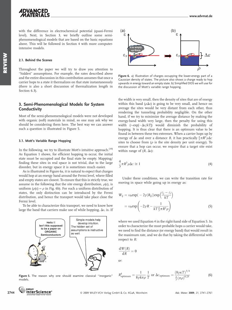
By using different material parameters, it was observed[11] thatthe fitting parameters Teff and Ef depend on the field strength(normalized by the distance between sites) and the phononictemperature of the media. However, in agreement with thegeneral prediction in Ref. [42], Teff and Ef are independent of thecharge-carrier concentration and the disorder parameter, be it sfor Gaussian disorder or E0 for exponential DOS. The effectivetemperature dependence on the applied electric field for a fixedlattice (phonon) temperature is shown in Figure 19. The circlesdenote the carrier temperature in exponential DOS and thesquares for Gaussian DOS. The solid lines are fits using the
Figure 18. a) Normalized charge density, current density, and density ofstates for Gaussian DOS of s# 4kT (T# 300K) under a negligible electricfield. The position of the Fermi levels is marked with a thick arrow, and thefilling factor of the DOS is 10$4. b) Same as in a)/cm, which induces ‘‘shiftupwards’’ of the carrier population. c) Same as in a) but for applied electricfield of 106 V and using the polaronic rate (Eq. 3), with a polaron bindingenergy of Ub# 0.4 eV, instead of the Miller–Abraham rate (Eq. 2).
2752 ! 2009 WILEY-VCH Verlag GmbH & Co. KGaA, Weinheim Adv. Mater. 2009, 21, 2741–2761
REVIE
W
www.advmat.de
dependence suggested in Ref. [43]:
!TEff=TL"2 # 1' %mEa=!kT=q"&2 (27)
We note that the original work[42] predicted the factor m to be0.5, and our fit results in 0.37, 0.02.
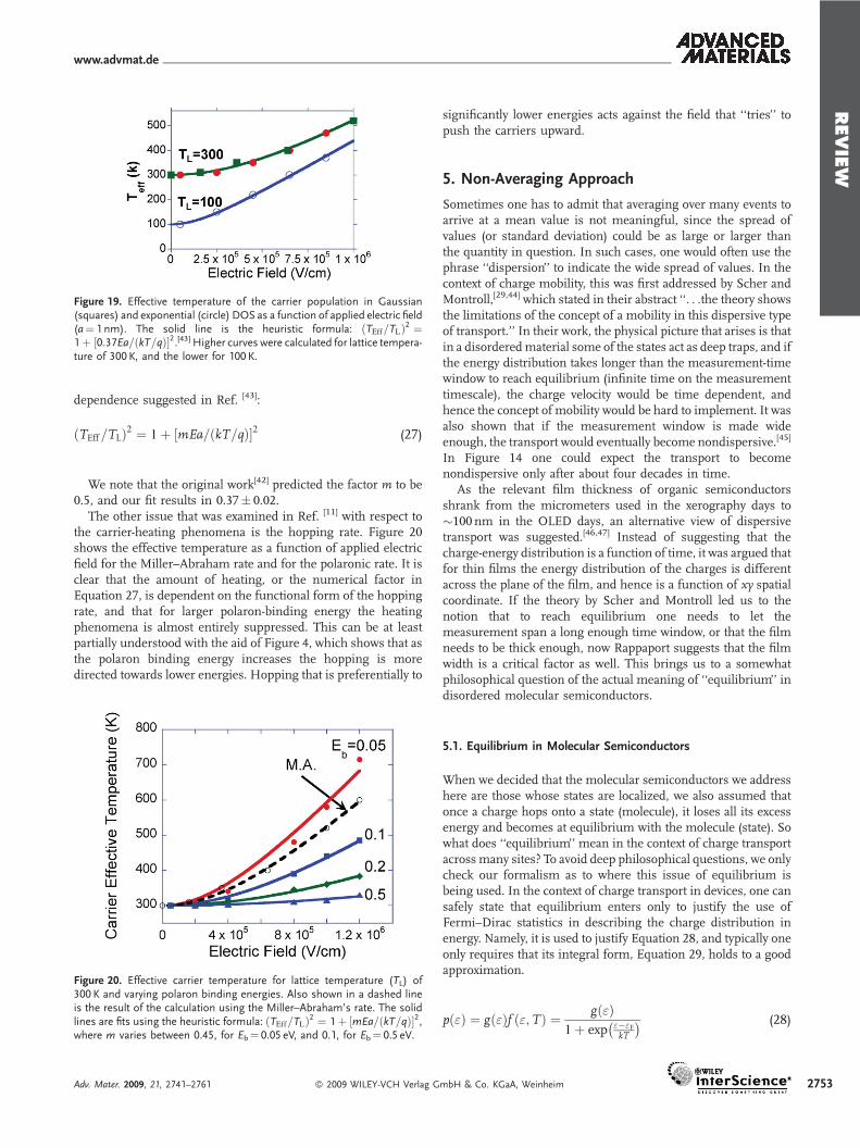
The other issue that was examined in Ref. [11] with respect tothe carrier-heating phenomena is the hopping rate. Figure 20shows the effective temperature as a function of applied electricfield for the Miller–Abraham rate and for the polaronic rate. It isclear that the amount of heating, or the numerical factor inEquation 27, is dependent on the functional form of the hoppingrate, and that for larger polaron-binding energy the heatingphenomena is almost entirely suppressed. This can be at leastpartially understood with the aid of Figure 4, which shows that asthe polaron binding energy increases the hopping is moredirected towards lower energies. Hopping that is preferentially to
significantly lower energies acts against the field that ‘‘tries’’ topush the carriers upward.
5. Non-Averaging Approach
Sometimes one has to admit that averaging over many events toarrive at a mean value is not meaningful, since the spread ofvalues (or standard deviation) could be as large or larger thanthe quantity in question. In such cases, one would often use thephrase ‘‘dispersion’’ to indicate the wide spread of values. In thecontext of charge mobility, this was first addressed by Scher andMontroll,[29,44] which stated in their abstract ‘‘. . .the theory showsthe limitations of the concept of a mobility in this dispersive typeof transport.’’ In their work, the physical picture that arises is thatin a disorderedmaterial some of the states act as deep traps, and ifthe energy distribution takes longer than the measurement-timewindow to reach equilibrium (infinite time on the measurementtimescale), the charge velocity would be time dependent, andhence the concept of mobility would be hard to implement. It wasalso shown that if the measurement window is made wideenough, the transport would eventually become nondispersive.[45]
In Figure 14 one could expect the transport to becomenondispersive only after about four decades in time.
As the relevant film thickness of organic semiconductorsshrank from the micrometers used in the xerography days to(100 nm in the OLED days, an alternative view of dispersivetransport was suggested.[46,47] Instead of suggesting that thecharge-energy distribution is a function of time, it was argued thatfor thin films the energy distribution of the charges is differentacross the plane of the film, and hence is a function of xy spatialcoordinate. If the theory by Scher and Montroll led us to thenotion that to reach equilibrium one needs to let themeasurement span a long enough time window, or that the filmneeds to be thick enough, now Rappaport suggests that the filmwidth is a critical factor as well. This brings us to a somewhatphilosophical question of the actual meaning of ‘‘equilibrium’’ indisordered molecular semiconductors.
5.1. Equilibrium in Molecular Semiconductors
When we decided that the molecular semiconductors we addresshere are those whose states are localized, we also assumed thatonce a charge hops onto a state (molecule), it loses all its excessenergy and becomes at equilibrium with the molecule (state). Sowhat does ‘‘equilibrium’’ mean in the context of charge transportacrossmany sites? To avoid deep philosophical questions, we onlycheck our formalism as to where this issue of equilibrium isbeing used. In the context of charge transport in devices, one cansafely state that equilibrium enters only to justify the use ofFermi–Dirac statistics in describing the charge distribution inenergy. Namely, it is used to justify Equation 28, and typically oneonly requires that its integral form, Equation 29, holds to a goodapproximation.
p!"" # g!""f !";T" # g!""1' exp "$"F
kT
& ' (28)
Figure 19. Effective temperature of the carrier population in Gaussian(squares) and exponential (circle) DOS as a function of applied electric field(a# 1 nm). The solid line is the heuristic formula: !TEff=TL"2 #1' %0:37Ea=!kT=q"&2.[43] Higher curves were calculated for lattice tempera-ture of 300 K, and the lower for 100 K.
Figure 20. Effective carrier temperature for lattice temperature (TL) of300 K and varying polaron binding energies. Also shown in a dashed lineis the result of the calculation using the Miller–Abraham’s rate. The solidlines are fits using the heuristic formula: !TEff=TL"2 # 1' %mEa=!kT=q"&2,where m varies between 0.45, for Eb# 0.05 eV, and 0.1, for Eb# 0.5 eV.
Adv. Mater. 2009, 21, 2741–2761 ! 2009 WILEY-VCH Verlag GmbH & Co. KGaA, Weinheim 2753

REVIE
W
www.advmat.de
P #Z
p!""d" #Z
g!""1' exp "$"F
kT
& ' d" (29)
In the above equations, only the DOS (g)is material or device/processing-dependent,hence we are led to examine its role or origin.In the previous Sections 3 and 4, we assumedthe sample to be infinite, and by DOS wemeant that it could reproduce the imaginaryexperiment in which we map all the states inthe infinite sample and create a histogramshowing the number (density) of states perenergy interval.
In order for the sample to be consideredinfinite, two conditions must be fulfilled: i) thesample should be large enough so that thehistogram of the states’ energy is independentof its size, and ii) every charge has sampled asignificant fraction of the sample (the charges‘‘know’’ that the sample is infinite). Figure 21illustrates point i), where Figure 21b and cshow the energetic surface created by 400sites, the energies of which were drawnrandomly from the Gaussian DOS shown asa solid line in Figure 21a. The contour (Fig. 21b) and surface (Fig.21c) show the typical roughness of the energy surface ofdisordered semiconductors. The dashed line in Figure 21a showsthe histogram of the 400 states, which looks relatively close to theoriginal DOS shown in the solid line. However, it should be clearthat if the fit is only close to being good at the center of theGaussian, it would be far from being reasonable at the tails(remember that low-density carriers reside at$s2/kT). So the ideaof the sample having to be large enough such that the actual DOSwould resemble the ‘‘theoretical’’ DOS becomes relatively obviouswith the aid of Figure 21. However, the notion that every chargehas to sample a significant fraction may be less obvious as oneneeds to put him/herself in place of the electron and imaginewhat it ‘‘sees.’’
To address this ‘‘seeing through the eyes of the charges’’, weexamine Figure 22. Figure 22a and b describes essentially thesame sample, but in Figure 22a the charges propagate along thelong axis, while in Figure 22b it is propagating along its short axisof the sample. In this figure, the sites are described as circles, andthe filling fraction of each circle corresponds to its energy.
Figure 22c shows the histogram of the sites energies for thesamples in Figure 22a and b, which is similar to the central regionof a Gaussian (shown in solid line). Now we place ourselves in theeyes of an electron, and try to visualize what it sees as it travelsacross the sample. If we send a charge across the sample, wewould expect it to sample a region having an area (volume) that isproportional to the propagation length. The yellowish (shadowedin B&W) square on the left side of sample b exemplifies such asampled region, and Figure 22d shows the histogram of the sitesenergy in that region.
The distribution in Figure 22d is so different to the one inFigure 22c that we can safely say that if Figure 22c describes theDOS function (g), then neither Equation 28 nor 29 could besatisfied in this sampled region. This leads us to one of twoconclusions: i) charges moving across a thin sample can neverbe at equilibrium; or ii) the Gaussian DOS is not appropriate todescribe the transport, and a more ‘‘local’’ version should beused (as in Fig. 22d). It is also clear that if we move theyellowish square to the right, we will produce different shapesfor the local DOS, or in other words, charges starting at different
positions would cross the sample under adifferent time with a different velocity.Namely, there is a variation or dispersionof the velocity that could be interpreted asdispersion in the mobility, and in this case itis a spatial dispersion.[46,47]
Turning to the long sample depicted inFigure 22a, we can imagine the same yellowishsquare expanding across it as a function oftime. Namely, the local DOS or the sampledDOS would gradually change from Figure 22dto c. This tells us that the velocity of charges isgoing to be time dependent, or that there is atime-domain dispersion of the mobility.[29,44]
Figure 22. a) Schematic description of a sample made of discrete hopping sites. Sites aredescribed as circles, and the filling fraction of each circle corresponds to its energy. b) Schematicdescription of the same sample but with different orientation with respect to the electric field. Thesquare area illustrates the volume sampled by a drifting carrier. c) DOS of the samples shown in a)and b). d) DOS experienced by a charge sampling the square area in b).
Figure 21. a) Hypothetical Gaussian DOS (solid line) and the histogram of 400 states (dashedline) drawn based on this Gaussian probability. b) Contour map of the 400 states (sites) drawn. c)3D surface map of the 400 states (sites) drawn.
2754 ! 2009 WILEY-VCH Verlag GmbH & Co. KGaA, Weinheim Adv. Mater. 2009, 21, 2741–2761

REVIE
W
www.advmat.de
This also helps us understand why if we take a sample big enoughand let the charges propagate for a long enough time they willeventually reach equilibrium and the transport would stop beingdispersive (see Fig. 14 and Ref.[45]). This also suggests that for thin(disordered)-film devices, where the charge-propagation time isby definition very short, the dispersive transport would constitutean almost intrinsic property.
To test the idea of the above non-averaging approach, anumerical simulation based on the master-equation approachwas conducted.[47] To be consistent with published literature,the numerical simulation was of a time of flight experiment,and the numerical experiment used a sample with dimensionsof 9 nm. 9 nm. 75 nm. The infinite-size sample was assumedto be relatively ordered, characterized by a Gaussian energydistribution having standard deviation of s# 3kT. The typicalprocedure for calculating the TOF response would be to drawdifferent samples (paths) until the average result becomesindependent of the number of draws made. Such a procedureresulted in the dashed line in Figure 23, illustrating that for thethin, 75 nm, film simulated, the transport is highly dispersive.However, the individual paths, denoted by round and squaresymbols, exhibit a distinct plateau over a significant fraction ofthe propagation time. Namely, the local transport, which isassociated with the local DOS, is not dispersive. From such anumerical experiment one can conclude that the dispersivenature of thin samples is largely due to spatial non-uniformities occurring on the nanometer (10 nm) scale.
5.2. Spatially Dispersive Transport or Mobility DistributionFunction
Based on the above discussion, we can say that spatially dispersivetransport allows sample to be viewed as if it was divided intosubunits or pathways (Fig. 24), each characterized by its localDOS and consequently by a typical charge velocity or mobility.The volume of this imaginary pathway would be roughly thevolume that a charge would sample as it drifts and diffusestowards the opposite contact.
If one excites the sample by generating electrons at the contactboundary using a step-function temporal shape, then at differentplaces charges would propagate at different speeds (see schematic
description in Fig. 24). The current flowing through the samplecan then be mathematically described as:[46]
Je!t" # APqZ1
d2Vt
g!me"dme 'Zd
2
Vt
0
g!me"t
ttr!me"dme
8>><
>>:
9>>=
>>;(30)
where Je is the electron current density, g(me) is the mobilitydistribution function (MDF) for the electron pathways, ttr(me) isthe transit time across the device for an electron with mobilityme
&ttr!me" # d2
meV
', d is the device thickness, q is the electron
charge, P is the incident light intensity, and A is the carrier pairgeneration efficiency (number of electron-hole pairs generatedper unit of incident intensity). The first term in the bracketsrepresents the pathways that have reached their steady state bytime t (have a mobility value higher than d2
tV). The second termrepresents paths with lower mobility, which have not reachedsteady state by time t. Equation 30 can be manipulated to form ananalytic expression for deriving the MDF:[46]
g!m" # gd2
Vt
! "# $ d2I!t"
dt22Vt3
APqd2(31)
We note that the above derivation assumed that for each paththe mobility can be defined and that temporal dispersion effectsare not significant. In cases where the disorder is large and thespatial distribution is also mixed with significant temporaldispersion, the MDF described above should read velocitydistribution function.
6. Implications and Uses for Device Analysis
6.1. The Density of States Function
As we have seen in the previous sections, there are differentmodels one may use for device analysis, and the preferredchoice may depend on the shape of the DOS. Hulea et al.[48] wereprobably the first to attempt a direct measurement of theelectronic DOS in semiconducting-molecule/polymer-basedfilms. Using electrochemical doping of OC1C10-PPV, they foundthat the DOS was essentially exponential, and that only at veryhigh densities (above 0.5 per monomer), which are probably
Figure 23. Time-resolved current transient as a result of an impulse chargeexcitation at x# t# 0 (simulation of classical time of flight). The round andsquare symbols are single-run results (specific paths), and the dashed lineis an average over many such runs. The sample length is 75 nm.
Figure 24. Illustration of spatial distribution of current paths (mobilityvalues) in a thin-film device. The minus signs illustrate the response to astep function charge injection at the top electrode.
Adv. Mater. 2009, 21, 2741–2761 ! 2009 WILEY-VCH Verlag GmbH & Co. KGaA, Weinheim 2755

REVIE
W
www.advmat.de
above any practical device-operating conditions, the DOS can besomewhat fitted to a Gaussian DOS. The only reservation withrespect to a measurement performed through electrochemicaldoping is that dopants tend to alter the DOS.[49,50] Figure 25shows the effect of doping on both exponential and GaussianDOS calculated using the formalism described in Refs.[49,50]. Onecan observe in Figure 25 that the transition from thedopant-induced exponential-like tail of the main DOS functionoccurs at a DOS value that is 10 times the doping level. We shouldalso mention that exponential-like tails are a general phenomenaassociated with random distribution of scattering potentials.[51]
Tal et al.[52] have developed a technique based on the use ofKelvin-probe measurements of the channel in a FETas a functionof gate bias. Data similar to the one published in Ref.[52] is shownin Figure 26, and it indicates that the DOS of an undoped a-NPDis Gaussian with an exponential tail. It also shows that by dopingto a level of 1018 cm$3, the DOS broadens, and that the deviationfrom a Gaussian occurs at a DOS value that is about 10 timeshigher (in agreement with the observation made on Fig. 25).Having this in mind, we return to the undoped DOS (solid line inFig. 26), and it seems now that we should refer to the undoped
sample as non-intentionally doped to a level of(1017 cm$3. However, the FET characteristicsshowed an ON (VGS#$7V) to OFF (VGS# 0V)ratio of 106,[53] which immediately rules outsuch high level of doping. It is tempting toconclude that the exponential tail is an intrinsicbulk phenomenon, but one has to rememberthat the measurement was done on a very thinTFT channel that was in close proximity withthe dielectric interface. Veres et al.[54] arguedthat the gate dielectric may induce broadeningof the DOS due to potential fluctuationsassociated with internal dipoles,[55] and wemay add that the low density of trapped chargesat the insulator would have a similar effect.
To conclude this section, we can only say thatthe DOS in organic semiconductors is probablya combination of a Gaussian and an exponen-tial DOS, where the relative contribution ofeach may depend on the purity of the film andthe device it is embedded in. For example, thediscussion above indicates that the role of
the insulator in organic TFTs is to enhance the contribution ofexponential-like tails, and that it would be reasonable to assumethat in some cases it may obscure any ‘‘intrinsic’’ DOS.
6.1.1. Generalized Einstein Relation
A property that is closely related to the shape of the DOS is theEinstein relation. One way of deriving the Einstein relation startsfrom the continuity equation Jh # mhnhE$Dh
ddx nh, and
assumes that the total current is very small compared to thedrift and diffusion currents !Jh + mhnhE; Dh!d=dx"nh", suchthat one can neglect it and writemh # Dh
1nh
dnhEdx # $Dh
1nh
dnhdV . The
last step is assuming equilibrium such that the voltage drop canbe replaced with the difference in Fermi level, and we arriveat mh # $Dh
1nh
dnhdEf
# $Dh1nh
ddEf
*R g!""1'exp
"$"FkT! " d"
+#D Dh
qkT
1hD.[1]
Knowing the states density as a function of energy (DOS) allowscalculating the Einstein relation as a function of the position ofthe Fermi level energy (charge density) relative to the DOS andvice versa.[21,56] An example of such calculation is shown inFigure 27, which uses Gaussian DOS of different widths and withNV# 1020 cm$3.
The fact that the enhancement of the Einstein relation (hD)actually tracks the DOS function is depicted in Figure 28 for aGaussian DOS with s# 4kT (T# 300K). The fraction of the DOSfilled by the charge carrier as a function of the Fermi level isshown in round symbols. The dotted line shows a dependence ofexp($DE/kT). We note that at charge densities above 10$5 of thetotal DOS the charge-density dependence becomes less sensitiveto changes in the Fermi level. Examining Figure 27 we note thatthis is exactly the energy at which the enhancement of theEinstein relation (hD) starts to grow. Also shown in Figure 28 isthe DOS function (square symbols).
6.2. Analyzing Disordered Organic TFTs
Effectively, most of the analysis applied to disordered organicmaterials is relying on them being disordered and not somuch on
Figure 25. Density of states as a function of energy. a) The bottom curve (square symbols) showsundoped exponential DOS (T0# 600K,Nt# 1021 cm$3), and the top one (round symbols) showsthe case of adding ionized dopants at a density of 1018 cm$3. b) The bottom curve (squaresymbols) shows undoped Gaussian DOS (s# 0.1 eV, NV# 1021 cm$3) and the top one (roundsymbols) shows the case of adding ionized dopants at a density of 1018 cm$3. The vertical linesshow the position of the Fermi level for a charge density of 1018 cm$3.
Figure 26. DOS versus energy relative to Etf (Ef at VGS#Vt) for undoped(solid triangles) and doped (solid circles) samples. The solid curves arefitting of a Gaussian function and an exponential tail to the undopedsample DOS.[52]
2756 ! 2009 WILEY-VCH Verlag GmbH & Co. KGaA, Weinheim Adv. Mater. 2009, 21, 2741–2761

REVIE
W
www.advmat.de
them being organic molecules. In that context, one should alsomention the vast literature developed for amorphous silicon(a-Si)-based TFTs.[57,58] In the field of a-Si, it is well accepted thatthe transport is affected by deep exponential-like trap states, andin the context of field effect transistors one uses the power lawdependence of the mobility:[59,60]
m # m0
VGS $ VT
VAA
! "g
(32)
or a channel-conductance formula of:
gch # WLCim0
1
VgAA
!VGS $ VT"1'g (33)
And if we use the fact that the channel width is to a goodapproximation proportional to (VGS$VT)
$1, then the 3D chargedensity (d) at the channel is proportional to (VGS$VT)
$2. Using
Equation 32, we find:
m # m0
dg=2AA
dg=2 (34)
If we substitute g/2 with T0/T or k, then Equation 34 becomessimilar to Equation 20 derived by Vissenberg and Matters[14] fortransport within an exponential DOS (see Section 3.3.2), orEquation 22 derived by Roichman et al.[24] for transport withinGaussian DOS (see Section 3.3.3). Analysis of TFTs based on theassumption that the mobility is governed by a power law isabundant in the a-Si literature, and is also used in the field oforganic semiconductors.[14,61]
There are several things to note while analyzing TFTs that arebased on a material exhibiting charge-density dependence of themobility.
Using the known formula m # LWCiVDS
@IDS@VGS
carries the hiddenassumption that @m
@VGS# 0.
There is also a field dependence of the mobility, plus at highVDS values the charge density across the channel is not uniform.Extracting at low drain-source voltages helps to overcome theseproblems.
In this context, it is worth mentioning the device analysispresented in Ref.[62], which showed that by careful design andmeasurement procedures it is possible to extract both chargedensity and electric-field dependence of the mobility. In thispaper, they used the model by Roichman et al.[24] or its concepts,which account also for electric-field dependence, to explain thephysical picture.
6.2.1. Channel depth and the Einstein Relation
It is possible to show that the channel depth (XChannel) can beapproximated[24] as
XChannel *dins
VG $ V!y""p"ins
kTqh (35)
Here dins and eins are the thickness and dielectric constant ofthe insulator, respectively. Ep is the dielectric constant of theorganic semiconductor, V(y) is the potential at the channel(VSource/V(y)/VDrain), and h is the Einstein enhancementfactor, which is charge-density dependent (see Fig. 27).Examining Equation 35 it seems that by applying high gate biasthe channel depth would shrink towards zero and consequentlythe charge density at the channel would increase with no limit.This is of course not physical, since the maximum charge densitycannot exceed the total DOS (NV). This is where h becomes veryimportant, and one can consider that, in the current context, hwould increase so as to enhance the channel depth and preventthe charge density from exceeding that of the DOS. Figure 29shows the calculation of the channel depth (round symbols) andthe charge density (square symbols) as a function of gate bias. Atfirst the channel depth does vary almost like 1/VG, but then itflattens at about 1 nm, and above 14V it starts slowly to increase.Accordingly, the charge density rises steeply at low gate bias, andthen only asymptotically approaches the total DOS
Figure 27. Enhancement of the Einstein relation, relative to the low-densitylimit (kT/q), as a function of the filling of the density of states.
Figure 28. DOS (square symbols, left axis) as a function of energy and thecharge density as a function of the Fermi-level energy (round symbols, rightaxis). The arrow indicates the onset of the DOS as would be determined incyclic voltammetery methods. The dashed line shows the slope of aBoltzmann factor. Note that at charge densities above 10$5–10$4 of thetotal density of sites the charge density becomes less sensitive to changesin the Fermi-level position.
Adv. Mater. 2009, 21, 2741–2761 ! 2009 WILEY-VCH Verlag GmbH & Co. KGaA, Weinheim 2757

REVIE
W
www.advmat.de
(NV# 1020 cm$3) as the increase in h prevents it from reachingNV.
6.3. Analyzing Disordered Organic LEDs
In organic LEDs, we are typically concerned not only withtransport within the layer but also in charge transport to adisordered media, charge transport between two layers, andcharge recombination, which is also transport limited.
6.3.1. Transport and Mobility
Regarding the transport itself, we can use Figure 17 to help usdecide which mechanism is most relevant for devices that are notcontact-limited. We can see that up to about 4 or 5V (across(100 nm) the charge-density dependence of the mobility is thegoverning factor, and above 5V it is the field dependence (viacarrier heating) of the mobility that is governing the I–V curve.Also, if the device has non-ideal contacts, then the charge densitywithin the device would not rise as much as a function of appliedvoltage, and hence the range where the field dependence isimportant will extend to lower voltages. This helps us rationalizewhy using themodel promoted by Bassler et al. (see Section 4 andEq. 24) was so successful in describing and analyzing theproperties of organic LEDs despite the fact that it does not accountfor charge-density effects.
6.3.2. Charge Injection
Injection into amorphous semiconductors can be analyzed byconsidering: i) fluctuation of injection barrier heights,[63,64] ii)hopping rates from a metal into a disordered (Gaussian)DOS,[65,66] iii) analyze the transport across the image potentialas overcoming the surface recombination rate at the contact,and[67,68] iv) charge transport across the image-force relatedbarrier assuming equilibrium conditions and accounting for theDOS.[69] The advantage of the 4th approach is that it relies onstandard device model equations, where the effect of the DOSshape can be entered through the generalized Einstein relation(see Fig. 30).
We should remember that the macroscopic semiconductordevicemodel is generally applied to thermalized carriers only, andhence if one wants to include the contact region in such a model,the thermalization length must be negligibly small. The issue ofthermalization length of carriers in the context of charge injectionis described in ref. [67], which treats the injection using onedimensional Onsager theory. From this paper, we only quote herethe approximate expression for the thermalization distance forhot carriers, xt*mn0(m/e), where v0 is the initial velocity of theinjected carrier, m is the mobility, and m is the carrier mass. Thisequation illustrates the relevance of the low-mobility to thephysical picture. Although the mass of a carrier-polaron is notwell known, the overall thermalization length is believed to be inthe range of 1–0.1 nm, and hence one may assume that thecarriers thermalize at first-hop site,[65] and that any furthermotion of the carrier is governed by hopping transport in theelectronic potential.
Using the 4th approach, it is possible to show that many of theunique features or ‘‘anomalies’’ in contact phenomena can betraced back to the simple fact that in a Gaussian DOS the changein charge density due to a change in Fermi level (contactworkfunction) does not follow the rule of exp($DE/kT)[69] (seeFig. 28). Detailed experimental studies, however, have shown thatsuch an approach on its own is not sufficient,[24] and that oneshould probably also allow for amodified DOS close to the contactinterface.[70,71] This observation along with the discussion inSection 6.1 strengthens the general statement that the DOS at theinterface, be it metal or insulator, is very likely to be different fromthe bulk one, and could impact measurable device properties.Despite the importance of the details of the DOS at the interfaceas a rule of thumb, one can state that a contact barrier of up toabout 0.4 eV is not likely to limit the current in the device at roomtemperatures.
6.3.3. Charge Transport Across Layers
On the semiconductor device model level, the transport in thedevice is governed by[72]
@
@tne!z; t" #
@
@zDe
@
@zne!z; t" ' me!E"ne!z; t"E!z; t"
( )
$ Re!z; t"ne!z; t" (36)
Figure 29. Calculated charge density and channel depth as a function ofgate bias for a disordered conjugatedmaterial. The calculated is for s# 7kTand NV# 1020 cm$3.
Figure 30. Schematic description of the mechanisms governing chargetransport across the metal-organic semiconductor interface.
2758 ! 2009 WILEY-VCH Verlag GmbH & Co. KGaA, Weinheim Adv. Mater. 2009, 21, 2741–2761

REVIE
W
www.advmat.de
At the interface between two materials, one would expect adiscontinuity that would affect the result of the @/@z on theright-hand side. In organic semiconductors, the mobility valuesvary by orders of magnitudes between different materials,[73] andthe electric-field dependence of it also varies between materials.This has led to the notion of mobility barrier, which could besignificant.[74,75] The other, more common, effect is that underquasi-equilibrium conditions a difference in the energy levelsshould result in a difference in the charge densities on both sidesof the interface, which in the case of Gaussian DOS could beformally written as:
N1 #R NV1##########
2ps1p exp $!"$ "01"2
2s21
!1
1' exp "$"FkTe
$ % d"
N2 #R NV2##########
2ps2p exp $!"$ "02"2
2s22
!1
1' exp "$"FkTe
$ % d"
8>>>>><
>>>>>:
As Figure 28 shows, a change in the relative position of theFermi level with respect to the DOS (e0$ eF) will result in achange in the equilibrium charge density. The other parametersthat are less obvious are the actual density of sites (NV), that couldvary as a function of the molecular structure, and especially whenmolecular blends are used, and the disorder (s). A careful readerwould notice that in the expression for the Fermi function wewrote Te. This implies that carrier heating will diminish the effectof the energy difference that is weighed by the temperaturedescribing the charge-energy distribution.
6.3.4. Charge Recombination & Light Emission
Charge recombination in organic LEDs is considered to be adiffusion-limited process or Langevin recombination process.The recombination is by nature a bimolecular process with a rateof the form RREC#BNP. The pre-factor B is calculated for aprocess in which the charges are being attracted by their mutualelectric field:
B # q"0"r
!me ' mh"?# q"0"r
!me!E" ' mh!E"" (37)
As discussed in previous sections, themobility is dependent onthe applied electric field. Can we expect the applied-electric-fieldeffect on the mobility to be relevant for the recombination rate oftwo charges that are randomly positioned with respect to eachother? If we consider only the Poole–Frankel-type effect oflowering the barriers in the direction of the field, then the answerwould probably be ‘‘no’’ or ‘‘very slightly.’’ The reasoning is thatthe field induced lowering of the barriers is occurring over a verylimited solid angle out of the full sphere describing the motiondirection of randomly positioned pairs. If we consider themechanism of carrier heating, where carriers are being elevatedin energy, then the answer would be a definite yes. The reasoninghere is that the higher position in energy is not-directional (inspace), and hence the mobility is enhanced not only in thedirection of the electric field. Again, Figure 17 tells us that above(5V themain contribution is due to carrier heating, and hence atvoltage above 5V one should definitely use field-dependentmobility in the recombination rate. In Ref. [76] this question was
addressed experimentally, with both the light output and chargedensity measured simultaneously in response to a square wavepulse of about 30V (see Fig. 31). Examining the turn-offdynamics, we note that at short times there is no correlationbetween the light and charge density inside the device, and that atlonger times they follow almost the same time dependence. If theinstantaneous drop in electroluminescence is not due to loweringof the charge density, then we are left only with the recombinationpre-factor B that could be changing (turning off) as the appliedvoltage (electric field) is removed. Namely, at high appliedvoltages the recombination prefactor must be written usingfield-dependent mobility, and in Ref. [77] it is shown to beimportant already at 5 V (across 75 nm). If one accepts that therecombination depends on the electric field in the same manneras the mobility is, it then becomes possible to monitor timeevolution of the electric field inside the device throughrecombination (light output) dynamics.[77]
6.4. Spatial Non-Uniformities
There could be many types of non-uniformities in devices,especially where contacts are involved or materials are beingadjoined. The most obvious sources are adhesion of metal layers,nonflat substrates (as spikes in non-ideal indium tin oxide (ITO)layers), the conductivity fluctuation across conducting polymers(as poly(3,4-ethylenedioxythiophene) (PEDOT)), and partialcrystallization.[78,79] To these, we have added, in Section 5.2,the spatial distribution of the mobility, which arises from thedisordered nature of most light-emitting materials. While it is notobvious if and what can be done to completely eliminate all thespatial non-uniformity, it is possible to post-characterize it anduse screening procedures to minimize the effect. Such could bebased on scanning probe techniques[80] or through the analysis ofdevice properties under step-function excitation conditions (seeFig. 32).[81]
It was suggested[81] that such non-uniformities affect thedevice lifetime, and that this is part of the reason for green-PPVbased devices having longer lifetimes. The other effect of any ofthe above-discussed non-uniformity types is related to thereduction in charge recombination and the consequent reductionin light-emission efficiency. The reasoning is that any non-uniformity is not likely to affect both electrons and holes in the
Figure 31. Measured light and charge density in a poly(p-phenylenevinylene) (PPV) LED in response to a short square pulse of 27 V.
Adv. Mater. 2009, 21, 2741–2761 ! 2009 WILEY-VCH Verlag GmbH & Co. KGaA, Weinheim 2759

REVIE
W
www.advmat.de
exact same manner. Hence, it would induce spatial separation,that would lower the device efficiency.[82]
6.5. ‘‘Extrinsic’’ heating
It is unthinkable to discuss the basic physics of organic LEDswithout touching a very critical factor such as joule heating. Asorganic LEDs are typically built on glass substrates, the heatdissipation is not efficient unless special measures are taken.[83,84]
One of the effects associated with current heating is typically theloss in device efficiency as the enhanced temperature affectselectrons and holes differently. While this effect is reversible,there could also be a thermal runaway[72] that would result in fastdegradation, probably through hot spots. Such thermal runawaycan be understood by considering that the current in proportional
to the mobility JSCL # 98 "m
V2
d3, and that the mobility is
temperature dependent, as described in Equations 24 or 25:
m!E;T" # m0exp*$ D
kT ' B&
1kT $ 1
kT0
'E0:5+. To these, we need
only to add the fact that the joule heating raises the devicetemperature above its heat-sink temperature (THS):T # THS ' IVRT. The lower limit for the effective thermalresistance (RT), for most experimental configuration, would be
close to that of the heat resistance of 1 mm3 glass, which is 110KW$1, and the actual value could easily be 10 times higher.
Figure 33 shows the j–V characteristics derived by solving thethree equations above self-consistently for a 1 mm2 device. Thefull line is calculated for RT# 0K W$1, the dashed-dotted line forRT# 160K W$1, and the dashed line for RT# 1600K W$1. Wenote that for the set of parameters used at around 10–15V, thedevice temperature would rise by about 30–50K, which wouldinduce a catastrophic thermal runaway of the current andtemperature. In practice, this thermal runaway would be lesssteep due to the presence of serial resistance, which is associatedwith the leads and contacts.
7. Summary
In this tutorial review, we have tried to describe several of thetheories or approaches abundant in the literature concerned withcharge transport. From the enormous number of contributions,we have tried to choose those which would help most to developsome intuition with respect to transport in organic-materials-based devices operating at, or not far from, roomtemperature. By nature, such a choice is highly subjective, and wehope that at least most of the important features were covered. Inthe first sections, we have also tried to emphasize that there isalways more than what just meets the eyes (our ‘‘Behind theScenes’’ sections), as this is extremely important in a material-driven field that is still evolving through the introduction of newmaterials, and where news specialists from different disciplinesare joining and bringing new/different views and outlooks.
Acknowledgements
We acknowledge support of the Israel Science Foundation and the RusselBerry Nanotechnology Institute at the Technion (RBNI). We thank D. Natalifor the fruitful comments.
Received: December 1, 2008Revised: January 14, 2009
Published online: May 7, 2009
[1] N. W. Ashcroft, N. D. Mermin, Solid State Physics, Holt, Rinehart and
Winston, New York 1988.
[2] P. W. Anderson, Phys. Rev. 1957, 109, 1492.
[3] M. A. Lampert, P. Mark, Current Injection in Solids, Academic Press, New
York 1970.
[4] M. Pope, C. E. Swenberg, Electronic Processes in Organic Crystals, Clarendon
Press, Oxford 1999.[5] A. Miller, E. Abrahams, Phys. Rev. 1960, 120, 745.
[6] N. F. Mott, W. D. Twose, Adv. Phys. 1961, 10, 107.
[7] T. Holstein, Ann. Phys. 1959, 8, 325.
[8] S. Guha, J. D. Rice, Y. T. Yau, C. M. Martin, M. Chandrasekhar, H. R.
Chandrasekhar, R. Guentner, P. S. de Freitas, U. Scherf, Phys. Rev. B 2003,
67, 125204.
[9] S. Guha, J. D. Rice, C. M. Martin, W. Graupner, M. Chandrasekhar, H. R.
Chandrasekhar, U. Scherf, Mater. Res. Soc. Symp. 2002, BB10. 7.1.
Figure 32. The mobility distribution function measured for two thin-layerdevices based on different light-emitting polymers: poly[2-methoxy-5-(2’-ethyl-hexyloxy)-1,4-phenylene vinylene] (MEH-PPV) and Green-PPV(structure details can be found in Ref. [81]).
10-4
10-3
10-2
10-1
100
101
300
310
320
330
340
350
360
0 5 10 15 20
Cur
rent
(Acm
-2)
Dev
ice
Tem
pera
ture
(K)
Applied Voltage (V)
RT = 0
RT =160
RT =1600
Figure 33. Calculation of the current density as a function of voltage for a 1mm2 device under constant-wave (CW) drive scheme and including jouleheating effects. The full line is calculated for RT# 0 K W$1, the dashed-dotted line for RT# 160 K W$1, and the dashed line for RT# 1600 K W$1.m0# 35 cm2 V$1 s$1, D# 4.8 eV, B# 2.9. 10$5 eV, and T0# 600K.
2760 ! 2009 WILEY-VCH Verlag GmbH & Co. KGaA, Weinheim Adv. Mater. 2009, 21, 2741–2761

REVIE
W
www.advmat.de
[10] N. F. Mott, Electronic Processes in Non-crystallineMaterials, Clarendon Press,
Oxford 1979.[11] Y. Preezant, N. Tessler, Phys. Rev. B 2006, 74, 235202.
[12] M. Yan, L. Rothberg, B. R. Hsieh, R. R. Alfano, Phys. Rev. B 1994, 49, 9419.
[13] V. Ambegaokar, B. I. Halperin, J. S. Langer, Phys. Rev. B 1971, 4, 2612.
[14] M. Vissenberg, M. Matters, Phys. Rev. B 1998, 57, 12964.[15] M. Vissenberg, Opto-Electronic Properties of Disordered Organic Semi-
conductors, Ph.D. Thesis, Universiteit Leiden, Leiden 1999.
[16] D. Monroe, Phys. Rev. Lett. 1985, 54, 146.[17] S. D. Baranovskii, T. Faber, F. Hensel, P. Thomas, J. Non-Cryst. Solids 1996,
200, 222.
[18] V. I. Arkhipov, P. Heremans, E. V. Emelianova, G. J. Adriaenssens, H.
Bassler, J. Phys. Condens. Matter 2002, 14, 9899.[19] H. C. F. Martens, I. N. Hulea, I. Romijn, H. B. Brom, W. F. Pasveer, M. A. J.
Michels, Phys. Rev. B 2003, 67, 121203.
[20] N. Tessler, Y. Roichman, Org. Electron. 2005, 6, 200.
[21] Y. Roichman, N. Tessler, Appl. Phys. Lett. 2002, 80, 1948.[22] S. D. Baranovskii, I. P. Zvyagin, H. Cordes, S. Yamasaki, P. Thomas, Phys.
Status Solid B Basic Res. 2002, 230, 281.
[23] S. Shaked, S. Tal, Y. Roichman, A. Razin, S. Xiao, Y. Eichen, N. Tessler, Adv.
Mater. 2003, 15, 913.
[24] Y. Roichman, Y. Preezant, N. Tessler, Phys. Status Solidi A Appl. Res. 2004,
201, 1246.
[25] Y. Roichman, Charge Transport in Conjugated Polymers, Ph.D. Thesis,
Technion Israel Institute of Technology, Haifa 2004, the thesis can be
found at http://www.ee.technion.ac.il/labs/orgelect/ under ‘‘published
papers’’ (Accessed on 1.3.2009).
[26] J. M. Ziman, Models of Disorder, Cambridge University Press, Cambridge
1979.
[27] H. Bassler, Phys. Status Solidi B 1993, 175, 15.
[28] M. Van der Auweraer, F. C. Deschryver, P. M. Borsenberger, H. Bassler, Adv.
Mater. 1994, 6, 199.[29] H. Scher, E. M. Montroll, Phys. Rev. B 1975, 12, 2455.
[30] Z. G. Yu, D. L. Smith, A. Saxena, R. L. Martin, A. R. Bishop, Phys. Rev. B
2001, 63, 085202.[31] D. M. Goldie, J. Non-Cryst. Solids 2000, 266, 294.
[32] J. Zhou, Y. C. Zhou, J. M. Zhao, C. Q.Wu, X. M. Ding, X. Y. Hou, Phys. Rev. B
2007, 75, 153201.
[33] W. F. Pasveer, J. Cottaar, C. Tanase, R. Coehoorn, P. A. Bobbert, P. W. M.
Blom, D. M. de Leeuw, M. A. J. Michels, Phys. Rev. Lett. 2005, 94, 206601.
[34] Y. N. Gartstein, E. M. Conwell, Chem. Phys. Lett. 1995, 245, 351.
[35] S. V. Novikov, D. H. Dunlap, V. M. Kenkre, P. E. Parris, A. V. Vannikov, Phys.
Rev. Lett. 1998, 81, 4472.[36] S. V. Novikov, A. V. Vannikov, J. Phys. Condens. Matter 1994, 6, 10519.
[37] U. Wolf, H. Bassler, P. M. Borsenberger, W. T. Gruenbaum, Chem. Phys.
1997, 222, 259.[38] H. Kageyama, K. Ohnishi, S. Nomura, Y. Shirota, Chem. Phys. Lett. 1997,
277, 137.
[39] A. Peled, L. B. Schein, D. Glatz, Phys. Rev. B 1990, 41, 10835.
[40] N. F. Mott, R. W. Gurney, Electronic Processes in Ionic Crystals, Oxford
University Press, London 1940.
[41] B. N. Limketkai, P. Jadhav, M. A. Baldo, Phys. Rev. B 2007, 75, 4.
[42] B. I. Shklovskii, E. I. Levin, H. Fritzsche, S. D. Baranovskii, in Transport,
Correlation and Structural Defects (Ed.: H. Fritzsche), World Scientific,
Singapore 1990, p. 161.
[43] S. Marianer, B. I. Shklovskii, Phys. Rev. B 1992, 46, 13100.
[44] H. Scher, M. F. Shlesinger, J. T. Bendler, Phys. Today 1991, 44, 26.[45] E. M. Horsche, D. Haarer, H. Scher, Phys. Rev. B 1987, 35, 1273.
[46] N. Rappaport, O. Solomesch, N. Tessler, J. Appl. Phys. 2006, 99, 064507.
[47] N. Rappaport, Y. Preezant, N. Tessler, Phys. Rev. B 2007, 76, 235323.
[48] I. N. Hulea, H. B. Brom, A. J. Houtepen, D. Vanmaekelbergh, J. J. Kelly, E. A.
Meulenkamp, Phys. Rev. Lett. 2004, 93, 166601.
[49] V. I. Arkhipov, P. Heremans, E. V. Emelianova, H. Bassler, Phys. Rev. B 2005,
71, 45214.
[50] V. I. Arkhipov, E. V. Emelianova, G. J. Adriaenssens, Phys. Rev. B 2001, 6308,081202.
[51] U. Pinsook, V. Sa-yakanit, Solid State Commun. 2008, 148, 42.
[52] O. Tal, Y. Rosenwaks, Y. Preezant, N. Tessler, C. K. Chan, A. Kahn, Phys.
Rev. Lett. 2005, 95, 256405.
[53] O. Tal, Electronic Properties of Organic Thin Films Studied by Kelivn Probe
Force Microscopy, Ph.D. Thesis, Tel-Aviv University, Tel-Aviv 2006.
[54] J. Veres, S. D. Ogier, S. W. Leeming, D. C. Cupertino, S. M. Khaffaf, Adv.
Funct. Mater. 2003, 13, 199.
[55] P. M. Borsenberger, H. Bassler, J. Chem. Phys. 1991, 95, 5327.
[56] O. Tal, I. Epstein, O. Snir, Y. Roichman, Y. Ganot, C. K. Chan, A. Kahn, N.
Tessler, Y. Rosenwaks, Phys. Rev. B 2008, 77, 201201.[57] R. A. Street, Technology and Applications of Amorphous Silicon, Spring-
er-Verlag, Berlin 1999.
[58] J. Kanicki, S. Martin, in Thin-Film Transistors, (Eds: C. R. Kagan, P. Andry),
Marcel Dekker, New York 2003.
[59] M. Shur, M. Hack, J. Appl. Phys. 1984, 55, 3831.
[60] L. Resendiz, M. Estrada, A. Cerdeira, Solid-State Electron. 2003, 47,
1351.
[61] G. Horowitz, P. Lang, M. Mottaghi, H. Aubin, Adv. Funct. Mater. 2004, 14,
1069.
[62] L. Fumagalli, M. Binda, D. Natali, M. Sampietro, E. Salmoiraghi, P. Di
Gianvincenzo, J. Appl. Phys. 2008, 104, 084513.[63] J. H. Werner, H. H. Guttler, J. Appl. Phys. 1991, 69, 1522.
[64] K. Maeda, Surf. Sci. 2001, 493, 644.
[65] V. I. Arkhipov, U. Wolf, H. Bassler, Phys. Rev. B 1999, 59, 7514.
[66] V. I. Arkhipov, E. V. Emelianova, Y. H. Tak, H. Bassler, J. Appl. Phys. 1998,84, 848.
[67] D. F. Blossey, Phys. Rev. B 1974, 9, 5183.
[68] J. C. Scott, G. G. Malliaras, Chem. Phys. Lett. 1999, 299, 115.[69] Y. Preezant, N. Tessler, J. Appl. Phys. 2003, 93, 2059.
[70] M. A. Baldo, S. R. Forrest, Phys. Rev. B 2001, 6408, 5201.
[71] B. N. Limketkai, M. A. Baldo, Phys. Rev. B 2005, 71, 085207.
[72] D. J. Pinner, R. H. Friend, N. Tessler, J. Appl. Phys. 1999, 86, 5116.[73] D. J. Pinner, R. H. Friend, N. Tessler, Synth. Met. 2001, 124, 41.
[74] B. K. Crone, P. S. Davids, I. H. Campbell, D. L. Smith, J. Appl. Phys. 2000, 87,
1974.
[75] D. J. Pinner, R. H. Friend, N. Tessler, J. Appl. Phys. 2005, 97, 014504.[76] N. Tessler, D. J. Pinner, V. Cleave, D. S. Thomas, G. Yahioglu, P. Lebarny, R.
H. Friend, Appl. Phys. Lett. 1999, 74, 2764.
[77] D. J. Pinner, R. H. Friend, N. Tessler, Appl. Phys. Lett. 2000, 76, 1137.[78] J. S. Kim, M. Granstrom, R. H. Friend, N. Johansson, W. R. Salaneck, R.
Daik, W. J. Feast, F. Cacialli, J. Appl. Phys. 1998, 84, 6859.
[79] M. Kemerink, S. Timpanaro, M. M. deKok, E. A. Meulenkamp, F. J.
Touwslager, J. Phys. Chem. B 2004, 108, 18820.[80] B. J. Leever, M. F. Durstock, M. D. Irwin, A. W. Hains, T. J. Marks, L. S. C.
Pingree, M. C. Hersam, Appl. Phys. Lett. 2008, 92, 013302.
[81] N. Rappaport, Y. Bar, O. Solomeshch, N. Tessler, Appl. Phys. Lett. 2006, 89,
252117.
[82] G. J. Adriaenssens, V. I. Arkhipov, Solid State Commun. 1997, 103, 541.
[83] N. Tessler, N. T. Harrison, D. S. Thomas, R. H. Friend, Appl. Phys. Lett.
1998, 73, 732.[84] J. C. Sturm, W. Wilson, M. Iodice, IEEE J. Selec. Topics Quantum Electron.
1998, 4, 75.
Adv. Mater. 2009, 21, 2741–2761 ! 2009 WILEY-VCH Verlag GmbH & Co. KGaA, Weinheim 2761