Chapter 6 Combinational-Circuit Building...
35
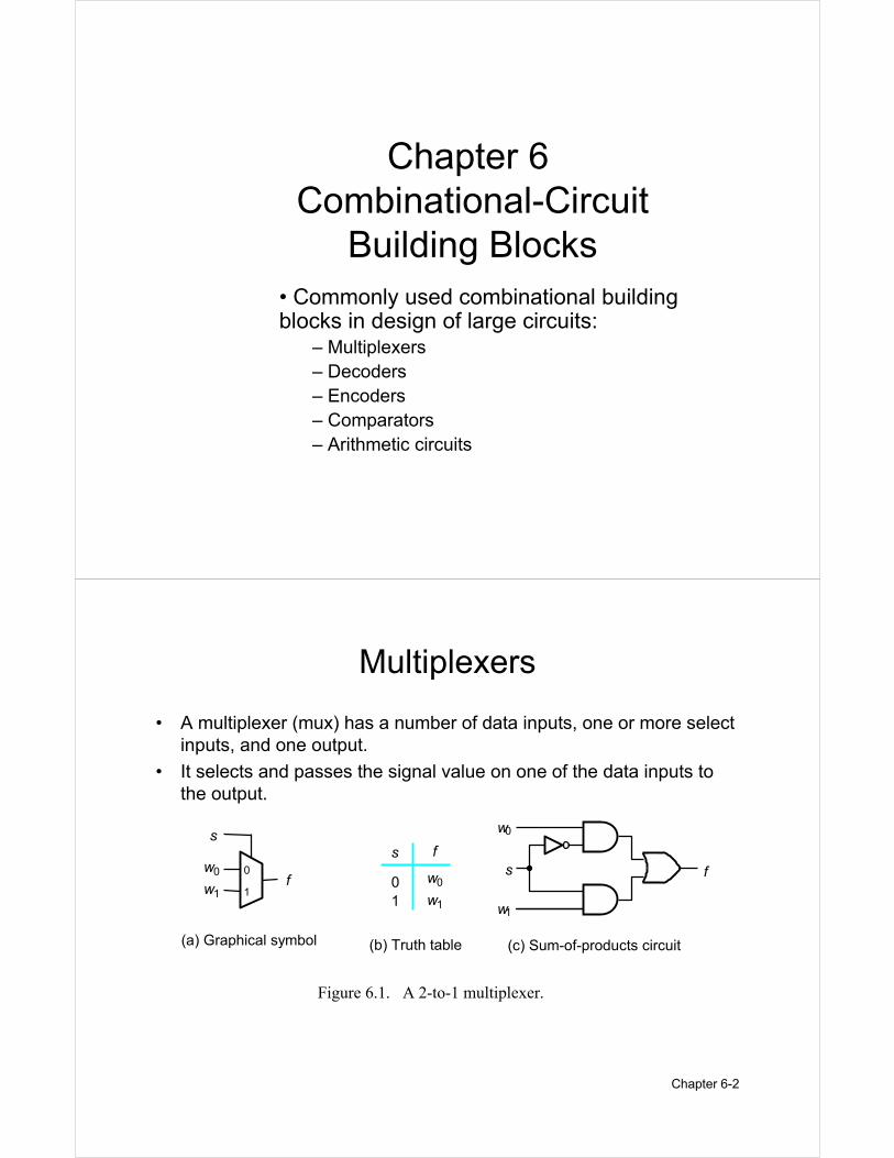
Chapter 6 Combinational-Circuit Building Blocks • Commonly used combinational building blocks in design of large circuits: – Multiplexers – Decoders – Encoders – Comparators – Arithmetic circuits Chapter 6-2 Multiplexers • A multiplexer (mux) has a number of data inputs, one or more select inputs, and one output. • It selects and passes the signal value on one of the data inputs to the output. (b) Truth table 0 1 f s w 0 w 1 (a) Graphical symbol f s w 0 w 1 0 1 (c) Sum-of-products circuit f s w 0 w 1 Figure 6.1. A 2-to-1 multiplexer.
Transcript of Chapter 6 Combinational-Circuit Building...
Chapter 6
Combinational-Circuit
Building Blocks
• Commonly used combinational building blocks in design of large circuits:
– Multiplexers
– Decoders
– Encoders
– Comparators
– Arithmetic circuits
Chapter 6-2
Multiplexers
• A multiplexer (mux) has a number of data inputs, one or more select
inputs, and one output.
• It selects and passes the signal value on one of the data inputs to
the output.
(b) Truth table
0
1
fs
w0
w1
(a) Graphical symbol
f
s
w0
w1
0
1
(c) Sum-of-products circuit
fs
w0
w1
Figure 6.1. A 2-to-1 multiplexer.
Chapter 6-3
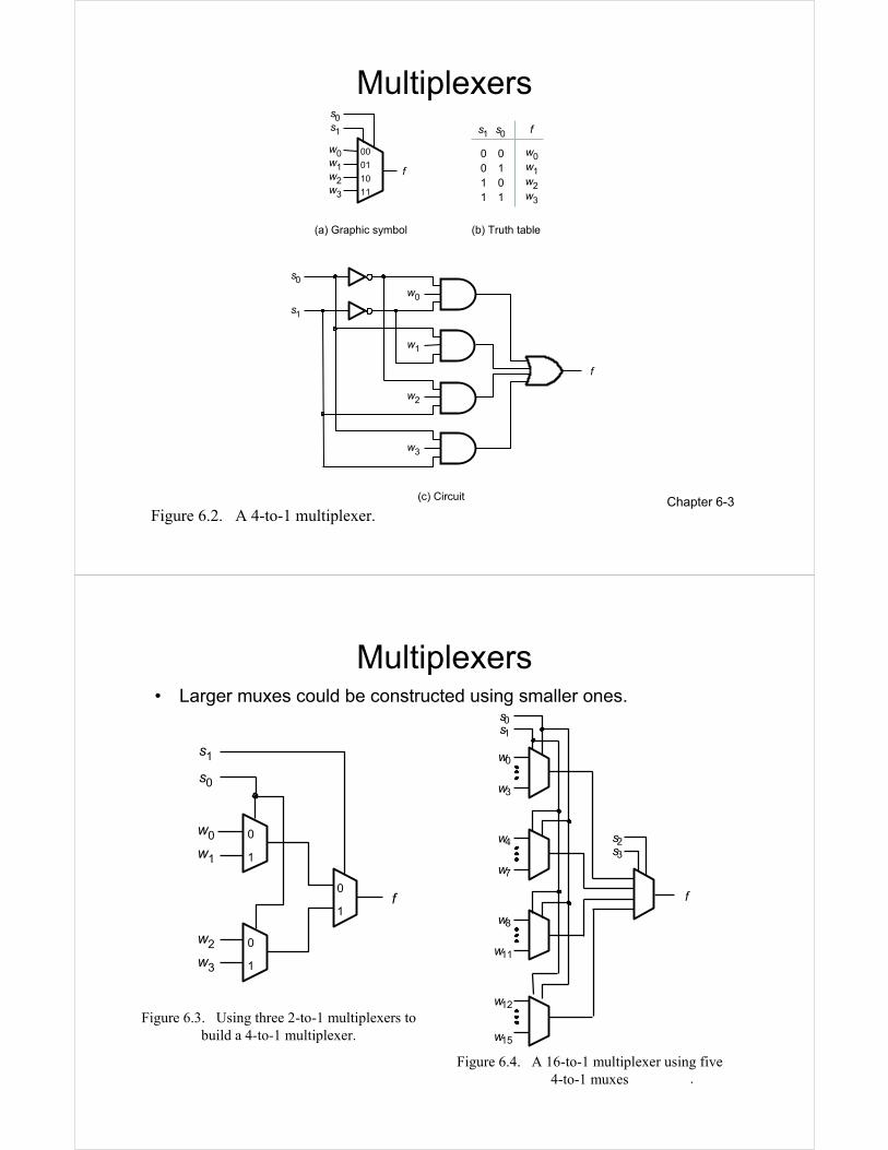
Multiplexers
f
s 1
w 0 w 1
00
01
(b) Truth table
w 0 w 1
s 0
w 2 w 3
10
11
0
0
1
1
1
0
1
f s 1
0
s 0
w 2 w 3
f
(c) Circuit
s 1
w 0
w 1
s 0
w 2
w 3
(a) Graphic symbol
Figure 6.2. A 4-to-1 multiplexer.
Chapter 6-4
Multiplexers• Larger muxes could be constructed using smaller ones.
0
w 0
w 1
0
1
w 2
w 3
0
1
f 0
1
s 1
s
Figure 6.3. Using three 2-to-1 multiplexers to
build a 4-to-1 multiplexer.
w 8
w 11
s 1
w 0
s 0
w 3
w 4
w 7
w 12
w 15
s 3
s 2
f
Figure 6.4. A 16-to-1 multiplexer using five
4-to-1 muxes

Chapter 6-5
Multiplexers• Refer to Fig 6.5 and 6.6 for practical application of muxes in implementation
of crossbars and programmable switches in FPGAs.
• General-purpose chips exist that contain muxes as their logic resources.
Actel Corp and QuickLogic Corp offer FPGAs in which the logic block
comprises muxes. TI offers gate array chips with mux based logic blocks.
• Muxes can also be used in a more general way to synthesize logic functions.
(a) Implementation using a 4-to-1 mux
f
w 1
0
1
0
1
w 2
1
0
0
0
1
1
1
0
1
f w 1
0
w 2
1
0 (b) Modified truth table
0
1
0
0
1
1
1
0
1
f w 1
0
w 2
1
0
0
1
f w 1
w 2
w 2
(c) Efficient implementation using 2-to-1 mux
f
w 2
w 1
Figure 6.7. Synthesis of an XOR gate
using a mux
Chapter 6-6
(a) Original and modified truth tables
w3
w3
00
0
1
1
1
0
1
fw1
0
w2
1
0 0
0 1
1 0
1 1
0
0
0
1
0 0
0 1
1 0
1 1
0
1
1
1
w1 w2 w3 f
0
0
0
0
1
1
1
1
f
w1
0
w2
1
(b) Circuit
w3
Figure 6.8. Implementation of the three-input majority function
using a 4-to-1 multiplexer.

Chapter 6-7
(a) Truth table
0 0
0 1
1 0
1 1
0
1
1
0
0 0
0 1
1 0
1 1
1
0
0
1
w1 w2 w3 f
0
0
0
0
1
1
1
1
w2 w3⊕
w2 w3⊕
f
w3
w1
(b) Circuit
w2
Figure 6.9. Three-input XOR implemented with
2-to-1 multiplexers.
Chapter 6-8
Figure 6.10. Three-input XOR function implemented with
a 4-to-1 multiplexer.
f
w 1
w 2
(a) Truth table (b) Circuit
0 0
0 1
1 0
1 1
0
1
1
0
0 0
0 1
1 0
1 1
1
0
0
1
w 1 w 2 w 3 f
0
0
0
0
1
1
1
1
w 3
w 3
w 3
w 3
w 3

Chapter 6-9
Shannon’s Expansion for synthesis
using muxes• Allows functions to be synthesized using combination of muxes and
other logic gates.
• Shannon’s Expansion theorem allows any Boolean function f to be
written in the form:
Example: Shannon expansion of the majority function in terms of w1
f(w1, w2, w3) = w1w2 + w1w3 + w2w3 = w1(w2w3) + w1(w2+w3)
f(w1, w2, . . . , wn) = w1• f(0, w2, . . . , wn) + w1 • f(1, w2, . . . , wn)
0 0 0 1 1 0 1 1
0 0 0 1
0 0 0 1 1 0 1 1
0 1 1 1
w 1 w 2 w 3 f
0 0 0 0 1 1 1 1
0 1
f w 1w 2w 3 w 2 w 3+ f
w 3
w 1w 2
Figure 6.11. The three-input majority function implemented
using a 2-to-1 multiplexer.
Chapter 6-10
Shannon’s Expansion for synthesis
using muxes• Shannon Expansion can be done
in terms of more than one
variable.
• If it is done on two variables the
resulting expression could be
implemented using a 4-to-1 mux.
• Note that if Shannon Expansion is
done in terms of all n variables,
then the result is the canonical
SOP of the function.
(a) Using a 2-to-1 multiplexer
f
w 2
w 1
w 3
f
w 1
w 2
w 3
(b) Using a 4-to-1 multiplexer
1
Figure 6.12. Synthesis of
f = w1w3 + w1w2 + w1w3
w 2
0 w 3
1
f
w 1
Figure 6.13. Three input majority
function using only 2-to-1 muxes
Chapter 6-11
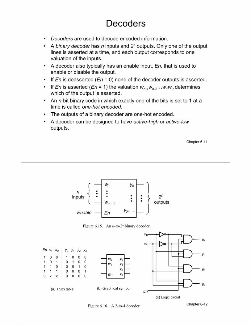
Decoders
• Decoders are used to decode encoded information.
• A binary decoder has n inputs and 2n outputs. Only one of the output
lines is asserted at a time, and each output corresponds to one
valuation of the inputs.
• A decoder also typically has an enable input, En, that is used to
enable or disable the output.
• If En is deasserted (En = 0) none of the decoder outputs is asserted.
• If En is asserted (En = 1) the valuation wn-1wn-2…w1w0 determines
which of the output is asserted.
• An n-bit binary code in which exactly one of the bits is set to 1 at a
time is called one-hot encoded.
• The outputs of a binary decoder are one-hot encoded.
• A decoder can be designed to have active-high or active-low
outputs.
Chapter 6-12
0
w n 1 –
n inputs
EnEnable
2 n
outputs
y 0
y 2 n 1 –
w
Figure 6.15. An n-to-2n binary decoder.
0
0
1
1
1
0
1
y 0 w 1
0
w 0
x x
1
1
0
1
1
En
0
0
0
1
0
y 1
1
0
0
0
0
y 2
0
1
0
0
0
y 3
0
0
1
0
0
w 0
En
y 0 w 1 y 1
y 2 y 3
(a) Truth table (b) Graphical symbol
(c) Logic circuit
w 1
w 0
y 0
y 1
y 2
y 3
En
Figure 6.16. A 2-to-4 decoder.
Chapter 6-13
w 2
w 0 y 0 y 1 y 2 y 3
w 0
En
y 0 w 1 y 1
y 2 y 3
w 0
En
y 0 w 1 y 1
y 2 y 3
y 4 y 5 y 6 y 7
w 1
Enw 0
En
y 0 w 1 y 1
y 2 y 3
y 8 y 9 y 10y 11
w 2
w 0 y 0 y 1 y 2 y 3
w 0
En
y 0 w 1 y 1
y 2 y 3
w 0
En
y 0 w 1 y 1
y 2 y 3
y 4 y 5 y 6 y 7
w 1
w 0
En
y 0 w 1 y 1
y 2 y 3
y 12y 13y 14y 15
w 0
En
y 0 w 1 y 1
y 2 y 3
w 3
En
Figure 6.17. A 3-to-8 decoder using two
2-to-4 decoders.
Figure 6.18. A 4-to-16 decoder built using
a decoder tree.
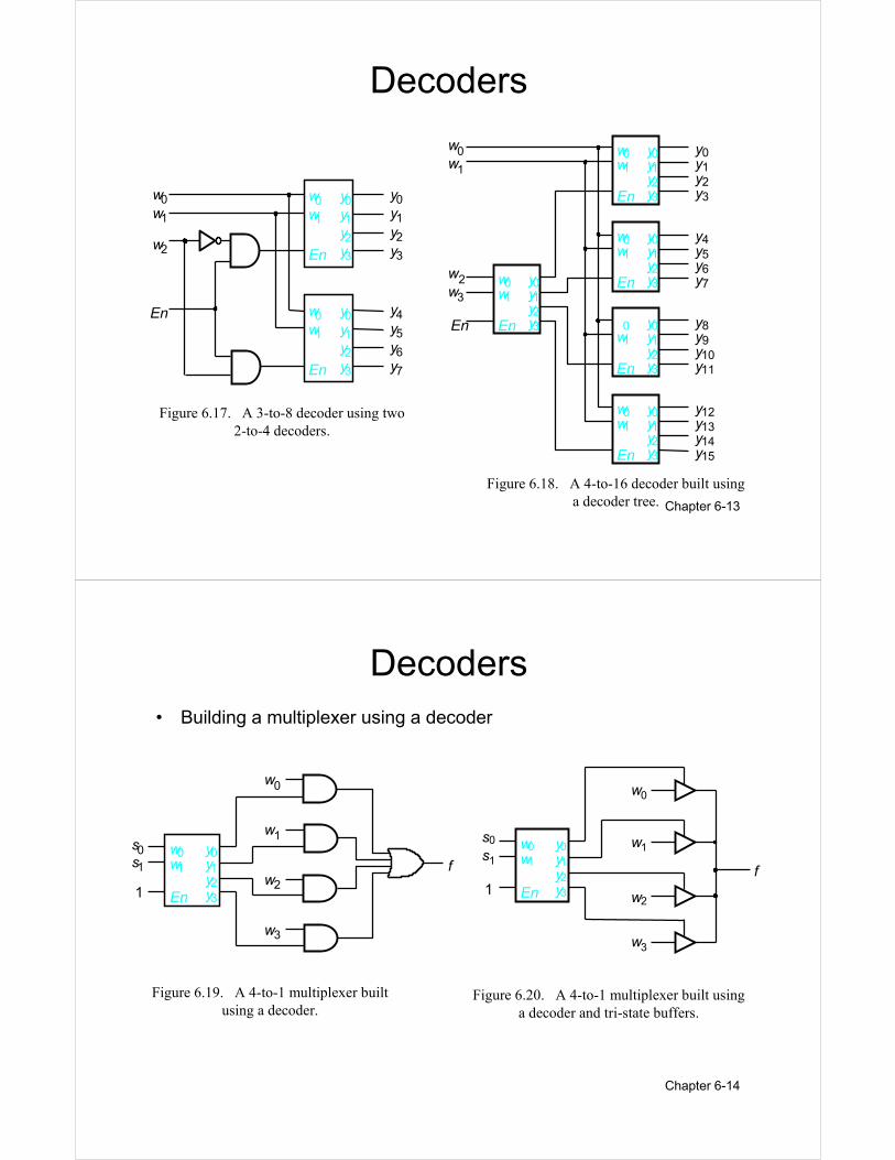
Decoders
Chapter 6-14
Decoders
• Building a multiplexer using a decoder
w 1
w 0
w 0
En
y 0 w 1 y 1
y 2 y 3
w 2
w 3
f
s 0 s 1
1
w1
w0
w0
En
y0w1 y1
y2y3
f
s0s1
1w2
w3
Figure 6.19. A 4-to-1 multiplexer built
using a decoder.Figure 6.20. A 4-to-1 multiplexer built using
a decoder and tri-state buffers.

Chapter 6-15
Decoders• One of the most important applications of decoders is for address decoding.
• The location of each row of memory cells is identified by its address.
• The first row has address 0 and the last row has address 2m-1, where m is the number of input
signals used for addressing.
• Information stored in a row of memory cells can be accessed by asserting the corresponding
select lines.
• A decoder with m inputs and 2m outputs is used to generate the select signals.
Sel 2
Sel 1
Sel 0
Sel 2 m 1 –
Address
Read
d 0 d n 1 – d n 2 –
m -to-2 m decoder
0/1 0/1 0/1
0/1 0/1 0/1
0/1 0/1 0/1
0/1 0/1 0/1
Data
a 0
a 1
a m 1 –
Figure 6.21. A 2m x n read-only
memory (ROM) block.
Chapter 6-16
Demultiplexers• A demultiplexer (demux) circuit performs the opposite of a mux, i.e.
switching the value of a single data input onto one of multiple data
output lines.
• An n-to-2n decoder can be used as a 1-to-2n demux.
• However, in practice decoder circuits are used more often as
decoders than as demuxes.
w 1
w 0
y 0
y 1
y 2
y 3
En
Example: a 2-to-4 decoder can be used
as a 1-to-4 data demultiplexer.
In this case the En input serves as the
data input for the demux, and the y0 to y3outputs are the data outputs.
The valuation of w1w0 determines which
of the outputs is set to the value of En.
Chapter 6-17
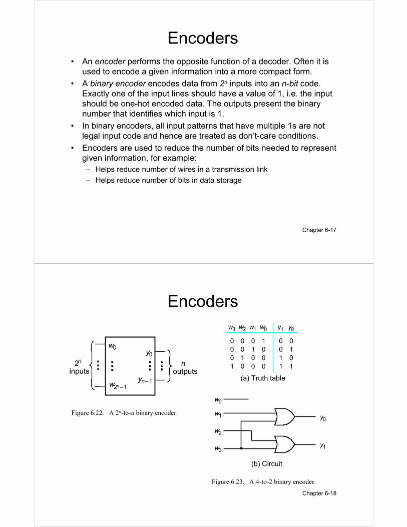
Encoders
• An encoder performs the opposite function of a decoder. Often it is
used to encode a given information into a more compact form.
• A binary encoder encodes data from 2n inputs into an n-bit code.
Exactly one of the input lines should have a value of 1, i.e. the input
should be one-hot encoded data. The outputs present the binary
number that identifies which input is 1.
• In binary encoders, all input patterns that have multiple 1s are not
legal input code and hence are treated as don’t-care conditions.
• Encoders are used to reduce the number of bits needed to represent
given information, for example:
– Helps reduce number of wires in a transmission link
– Helps reduce number of bits in data storage
Chapter 6-18
Encoders
2 n
inputs
w 0
w 2 n 1 –
y 0
y n 1 –
n outputs
(b) Circuit
0
0
1
1
1
0
1
w 3 y 1
0
y 0
0
0
1
0
w 2
0
1
0
0
w 1
1
0
0
0
w 0
0
0
0
1
w 1
w 0
y 0
w 2
w 3 y 1
(a) Truth table
Figure 6.23. A 4-to-2 binary encoder.
Figure 6.22. A 2n-to-n binary encoder.

Chapter 6-19
Priority Encoders• In a priority encoder each input has a priority level associated with it.
• The encoder output indicates the active input that has the highest
priority.
• When an input with a high priority is asserted, the other inputs with
lower priority are ignored.
Example: In the 4-to-2 priority encoder truth table (Fig 6.24) we assume
w0 has the lowest priority and w3 has the highest priority.
The outputs y1 and y0 represent the binary number that identifies the
highest priority input set to 1.
Since it is possible that all of the inputs could be left de-asserted (i.e.
equal to 0), an output z is provided to indicate this condition.
z is set to 1 when at least one of the inputs is equal to 1. It is set to 0
when all inputs are equal to 0.
When z = 0, the outputs y1 and y0 are meaningless (don’t cares).
Chapter 6-20
Priority Encoders• A logical circuit that implements the truth table can
be synthesized by using the techniques studied earlier.
• A more convenient way is to define a set of intermediate signals, i0, …, i3, such that each signal ik is equal to 1 only if the input with the same index, wk, represents the highest-priority input that is set to 1.
• Thus,
• Using the intermediate signals, the circuit for the priority encoder will have the same structure as the binary encoder in Fig 6.23 with
y0 = i1 + i3y1 = i2 + i3
and z = i0 + i1 + i2 + i3
d001
010
w0 y1
d
y0
1 1
01
1
11
z
1xx
0
x
w1
01x
0
x
w2
001
0
x
w3
000
0
1
Figure 6.24. Truth table for a 4-to-2
priority encoder.
i0 = w3w2w1w0
i1 = w3w2w1
i2 = w3w2i3 = w3
Chapter 6-21
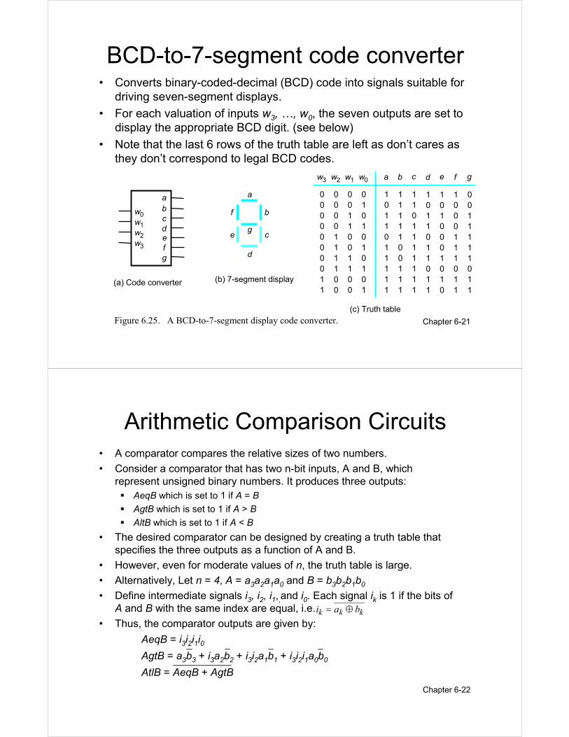
BCD-to-7-segment code converter• Converts binary-coded-decimal (BCD) code into signals suitable for
driving seven-segment displays.
• For each valuation of inputs w3, …, w0, the seven outputs are set to
display the appropriate BCD digit. (see below)
• Note that the last 6 rows of the truth table are left as don’t cares as
they don’t correspond to legal BCD codes.
w 0
a
w 1
b
c
d w 2 w 3
e
f
g
c e
a
g
b f
d
1
0
1
1
1
1
1
w 0 a
1
b
0 1
1
1
1
0
1
1
0
1
0
0
w 1
0
1
1
0
0
w 2
0
0
0
0
1
w 3
0
0
0
0
0
c
1
0
1
0
0
1
1
0
1
1
1
0
0
0
0
1
1 0 0 1
1
1
1
1
0
1
1
0
1 1
1
1
1
1
1
0
1
1
1
d
0
1
0
0
1
0
e
1
0
1
1
1
0
1
0
0
1
0
0
0
1
f
1
0
0
1
1
1
g
1
0
1
1
1
1
1
1
0
1 (a) Code converter (b) 7-segment display
(c) Truth table
Figure 6.25. A BCD-to-7-segment display code converter.
Chapter 6-22
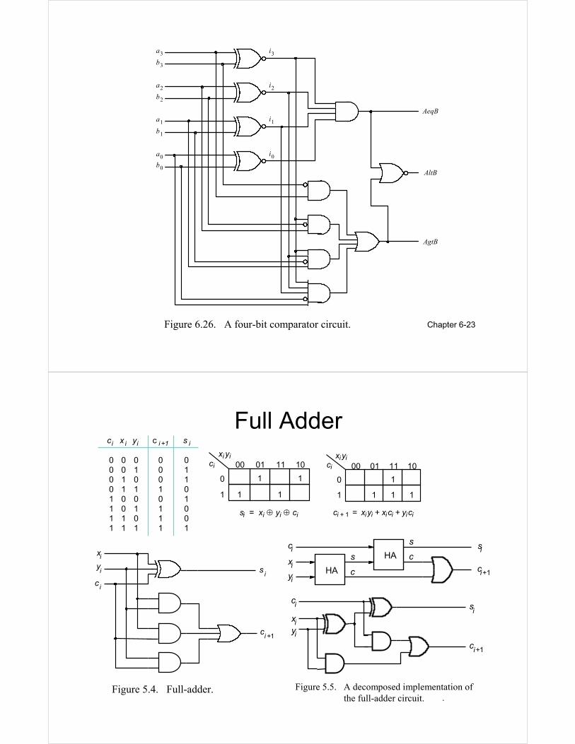
Arithmetic Comparison Circuits
• A comparator compares the relative sizes of two numbers.
• Consider a comparator that has two n-bit inputs, A and B, which
represent unsigned binary numbers. It produces three outputs:
� AeqB which is set to 1 if A = B
� AgtB which is set to 1 if A > B
� AltB which is set to 1 if A < B
• The desired comparator can be designed by creating a truth table that
specifies the three outputs as a function of A and B.
• However, even for moderate values of n, the truth table is large.
• Alternatively, Let n = 4, A = a3a2a1a0 and B = b3b2b1b0• Define intermediate signals i3, i2, i1,,and i0. Each signal ik is 1 if the bits of
A and B with the same index are equal, i.e.
• Thus, the comparator outputs are given by:
AeqB = i3i2i1i0
AgtB = a3b3 + i3a2b2 + i3i2a1b1 + i3i2i1a0b0
AtlB = AeqB + AgtB
kkk bai ⊕=
Chapter 6-23
i 0
i 1
i 2
i 3
b 0
a 0
b 1
a 1
b 2
a 2
b 3
a 3
AeqB
AgtB
AltB
Figure 6.26. A four-bit comparator circuit.
Chapter 6-24
Full Adder
00 01 11 10
0
1
x i y i c i
1
1
1
1
s i x i y i c i ⊕ ⊕ =
00 01 11 10
0
1
x i y i c i
1
1 1 1
c i 1 + x i y i x i c i y i c i + + =
0 0 0 1 0 1 1 1
c i 1 +
0 0 0 0 1 1 1 1
0 0 1 1 0 0 1 1
0 1 0 1 0 1 0 1
c i x i y i
0 1 1 0 1 0 0 1
s i
c i
x i
y i s
i
c i 1 +
Figure 5.4. Full-adder.
HA
HAs
c
s
c
c i
x i
y i c i 1 +
s i
c i
x i y i
c i 1 +
s i
Figure 5.5. A decomposed implementation of
the full-adder circuit.

Chapter 6-25
Ripple-Carry Adder• Cascade n full-adders using the carry signals to implement an n-bit
adder.
• The carry bit propagates from lower to higher significant adder units.
• Each adder introduces a time delay, say ∆t, before its si and ci+1outputs are valid.
• The delay for the complete sum and carry out to be available is n∆t.
• The circuit is called ripple-carry adder because of the way the carry
signals “ripple” through the full adder stages.
FA
x n –1
c n
c n-1
y n 1 –
s n 1 –
FA
x 1
c 2
y 1
s 1
FA
c 1
x 0 y 0
s 0
c 0
MSB position LSB position
Figure 5.6. An n-bit ripple-carry adder.
Chapter 6-26
n-bit Adder Application Example• Build a circuit that multiplies an eight-bit unsigned number by 3.
• Let, A = a7a6…a1a0 denote the number and P = p0p1…p1p0 denote the
product P = 3A. Note that 10 bits are needed to represent the product.
7 x 0 y 7 y 0
x 7 x 0 y 8 y 0 y 7 x 8
s 0 s 7
c 7
0
s 0 s 8
c 8
P 9 P 8 P 0 P 3 A = :
(a) Naive approach
a 7 A : a 0
x
x 1 x 0 y 8 y 0 y 7 x 8
s 0 s 8
c 8
0 0
a 7 A :
P 9 P 8 P 0 P 3 A = :
(b) Efficient design
a 0
Figure 5.7. Circuit that multiplies an eight-bit unsigned number by 3.
Chapter 6-27
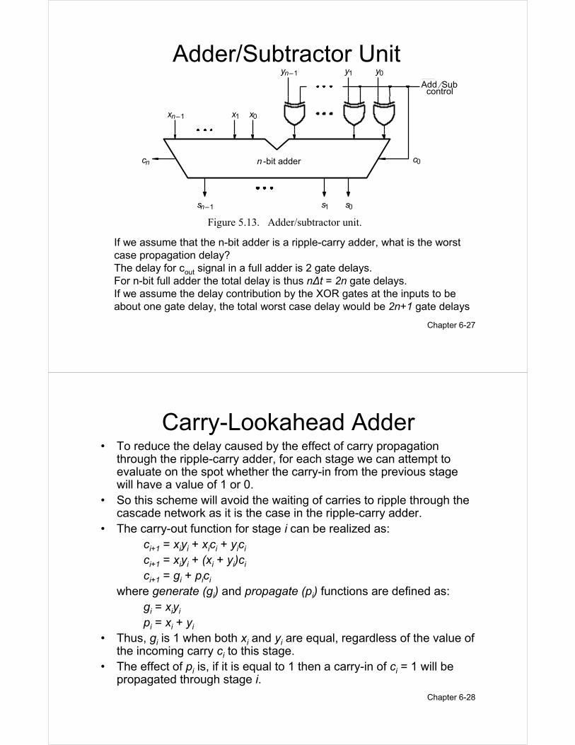
Adder/Subtractor Unit
s 0 s 1 s n 1 –
x 0 x 1 x n 1 –
c n n -bit adder
y 0 y 1 y n 1 –
c 0
Add ⁄ Sub control
Figure 5.13. Adder/subtractor unit.
If we assume that the n-bit adder is a ripple-carry adder, what is the worst
case propagation delay?
The delay for cout signal in a full adder is 2 gate delays.
For n-bit full adder the total delay is thus n∆t = 2n gate delays.
If we assume the delay contribution by the XOR gates at the inputs to be
about one gate delay, the total worst case delay would be 2n+1 gate delays
Chapter 6-28
Carry-Lookahead Adder• To reduce the delay caused by the effect of carry propagation
through the ripple-carry adder, for each stage we can attempt to evaluate on the spot whether the carry-in from the previous stage will have a value of 1 or 0.
• So this scheme will avoid the waiting of carries to ripple through the cascade network as it is the case in the ripple-carry adder.
• The carry-out function for stage i can be realized as:
ci+1 = xiyi + xici + yicici+1 = xiyi + (xi + yi)cici+1 = gi + pici
where generate (gi) and propagate (pi) functions are defined as:
gi = xiyipi = xi + yi
• Thus, gi is 1 when both xi and yi are equal, regardless of the value of the incoming carry ci to this stage.
• The effect of pi is, if it is equal to 1 then a carry-in of ci = 1 will be propagated through stage i.
Chapter 6-29
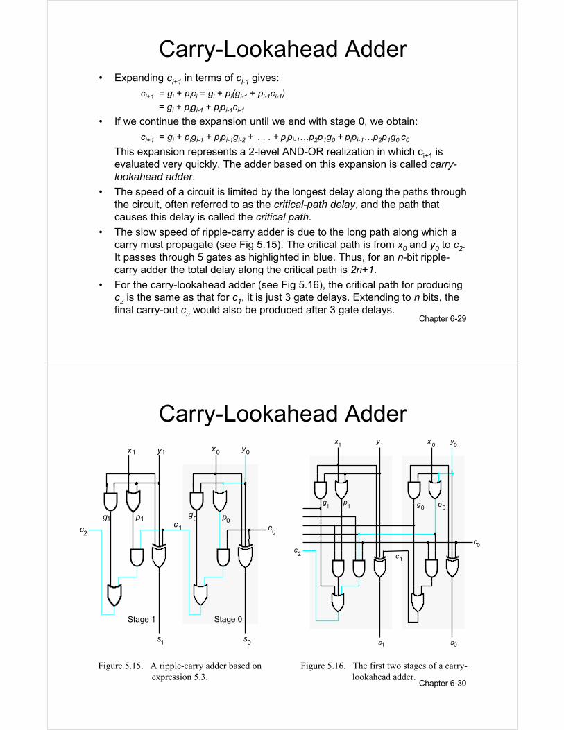
Carry-Lookahead Adder• Expanding ci+1 in terms of ci-1 gives:
ci+1 = gi + pici = gi + pi(gi-1 + pi-1ci-1)
= gi + pigi-1 + pipi-1ci-1
• If we continue the expansion until we end with stage 0, we obtain:
ci+1 = gi + pigi-1 + pipi-1gi-2 + . . . + pipi-1…p2p1g0 + pipi-1…p2p1g0 c0
This expansion represents a 2-level AND-OR realization in which ci+1 is
evaluated very quickly. The adder based on this expansion is called carry-
lookahead adder.
• The speed of a circuit is limited by the longest delay along the paths through
the circuit, often referred to as the critical-path delay, and the path that
causes this delay is called the critical path.
• The slow speed of ripple-carry adder is due to the long path along which a
carry must propagate (see Fig 5.15). The critical path is from x0 and y0 to c2.
It passes through 5 gates as highlighted in blue. Thus, for an n-bit ripple-
carry adder the total delay along the critical path is 2n+1.
• For the carry-lookahead adder (see Fig 5.16), the critical path for producing
c2 is the same as that for c1, it is just 3 gate delays. Extending to n bits, the
final carry-out cn would also be produced after 3 gate delays.
Chapter 6-30
Carry-Lookahead Adder
x 1 y 1
g 1 p 1
s 1
Stage 1
x 0 y 0
g 0 p
0
s 0
Stage 0
c 0
c 1 c 2
x 1
y 1
g 1
p 1
s 1
x 0 y 0
s 0
c 2
x 0
y 0
c 0
c 1
g 0
p 0
Figure 5.15. A ripple-carry adder based on
expression 5.3.
Figure 5.16. The first two stages of a carry-
lookahead adder.
Chapter 6-31
Carry-Lookahead Adderx 1 y 1
g 1 p 1
s 1 s 0
c 2
x 0 y 0
c 0
c 1
g 0 p 0
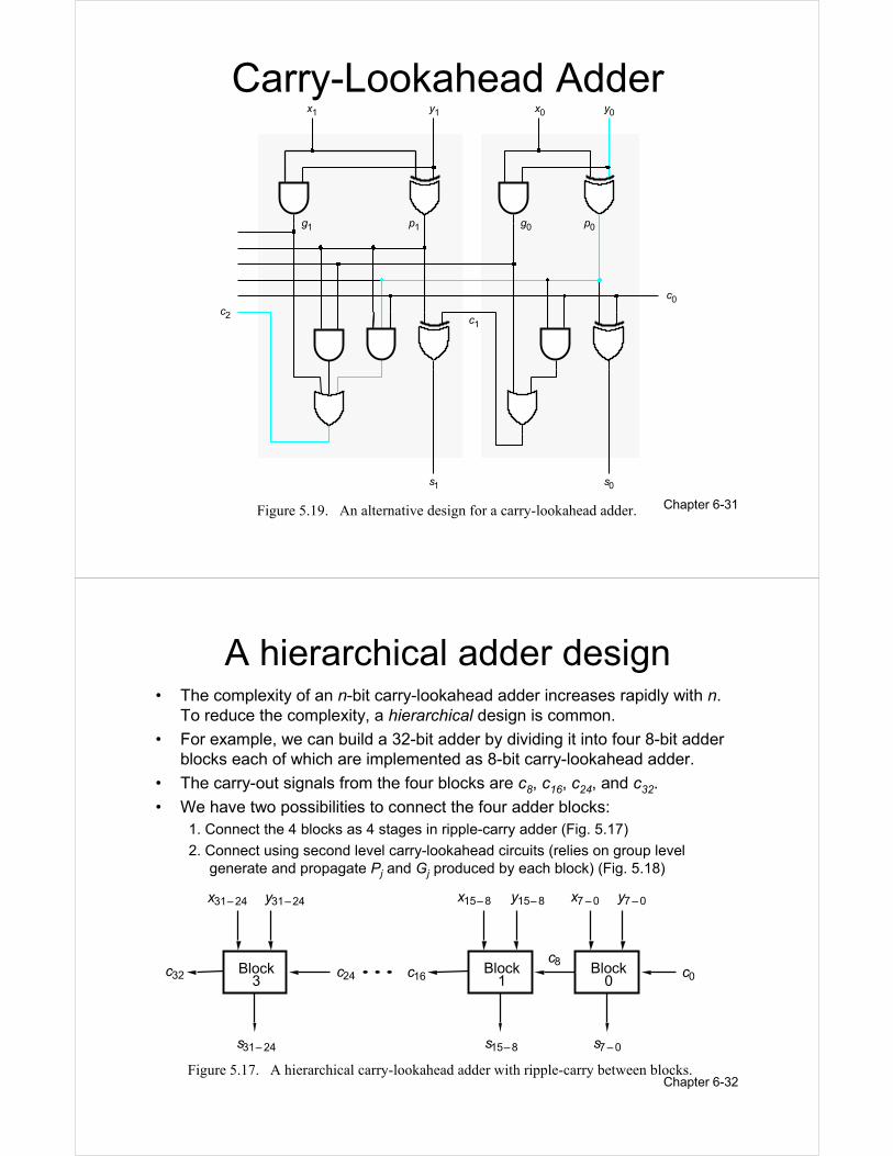
Figure 5.19. An alternative design for a carry-lookahead adder.
Chapter 6-32
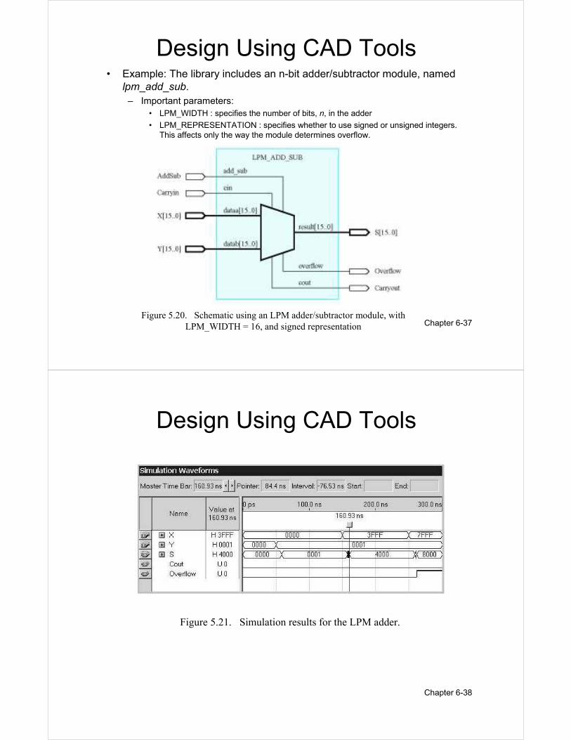
A hierarchical adder design• The complexity of an n-bit carry-lookahead adder increases rapidly with n.
To reduce the complexity, a hierarchical design is common.
• For example, we can build a 32-bit adder by dividing it into four 8-bit adder
blocks each of which are implemented as 8-bit carry-lookahead adder.
• The carry-out signals from the four blocks are c8, c16, c24, and c32.
• We have two possibilities to connect the four adder blocks:
1. Connect the 4 blocks as 4 stages in ripple-carry adder (Fig. 5.17)
2. Connect using second level carry-lookahead circuits (relies on group level
generate and propagate Pj and Gj produced by each block) (Fig. 5.18)
Block
x31 24–
c32 c24
y31 24–
s31 24–
x15 8–
c16
y15 8–
s15 8–
c8
x7 0– y7 0–
s7 0–
c03Block1
Block0
Figure 5.17. A hierarchical carry-lookahead adder with ripple-carry between blocks.

Chapter 6-33
A hierarchical adder design
Block
x 15 8 – y 15 8 – x 7 0 – y 7 0 –
3 Block 1
Block 0
Second-level lookahead
c 0
s 7 0 –
P 0 G 0 P 1 G 1 P 3 G 3
s 15 8 –s 31 24–
c 8 c 16c 32
x 31 24– y 31 24–
c 24
Figure 5.18. A hierarchical carry-lookahead adder.
Chapter 6-34
BCD Addition• Care has to be taken when adding two BCD digits since the sum
may become invalid (i.e. exceed 9).
• Let X = x3x2x1x0 and Y = y3y2y1y0 represent two BCD digits and let S = s3s2s1s0 be the desired sum digit, S = X + Y.
• If X + Y ≤ 9, then the addition is just like addition of two 4-bit unsigned numbers.
• But, if X + Y > 9, then the result requires two BCD digits, moreover the 4-bit sum obtained from the 4-bit adder may be incorrect. Thus in this case a correction needs to be applied to the result.
• The necessary correction arises from the fact that 4-bit binary addition is a modulo-16 scheme, whereas decimal addition is a modulo-10 scheme.
• Therefore, a correct decimal digit can be generated by adding 6 to the result of the 4-bit addition whenever it exceeds 9.
Z = X + Y
If Z ≤ 9, then S = Z and carry-out = 0
if Z > 9, then S = Z + 6 and carry-out = 1

Chapter 6-35
BCD Addition
4-bit adder
Detect if
MUX
4-bit adder
sum 9 >
6 0
X Y
Z
c out
c incarry-out
Adjust
S
0
c out
Four-bit adder
Two-bit adder
s 3 s 2 s 1 s 0
z 3 z 2 z 1 z 0
x 3 x 2 x 1 x 0 y 3 y 2 y 1 y 0
c in
Figure 5.36. Block diagram for a
one-digit BCD adder.Figure 5.38. Circuit for a one-digit BCD adder.
Chapter 6-36
Design Using CAD Tools• Schematic capture tools provide a library of graphical symbols that
represent basic logic gates. These gates are used to create
schematics of relatively simple circuits.
• Most tools also provide a library of commonly used circuits or
modules, such as adders. Each module can be imported into a
schematic as part of a larger circuit.
• In some CAD systems such modules are called macrofunctions or
megafunctions.
• Two main types of macrofunctions:
1. Technology-dependent macrofunction – designed for specific type of chip
2. Technology-independent macrofunction – can be implemented in any type of
chip.
• Library of Parameterized Modules (LPM) is included as part of the
Quartus II CAD system.
– Each module in the library is technology independent
– Each module is parameterized, i.e. it can be used in a variety of ways that can be
configured by using the CAD tools.
Chapter 6-37
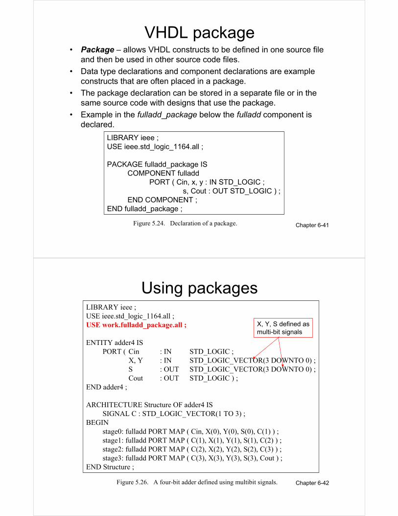
Design Using CAD Tools• Example: The library includes an n-bit adder/subtractor module, named
lpm_add_sub.
– Important parameters:
• LPM_WIDTH : specifies the number of bits, n, in the adder
• LPM_REPRESENTATION : specifies whether to use signed or unsigned integers.
This affects only the way the module determines overflow.
Figure 5.20. Schematic using an LPM adder/subtractor module, with
LPM_WIDTH = 16, and signed representation
Chapter 6-38
Design Using CAD Tools
Figure 5.21. Simulation results for the LPM adder.

Chapter 6-39
n-bit adder in VHDL
• Hierarchical design of an n-bit ripple-carry adder using n instances
of full-adders.
LIBRARY ieee ;
USE ieee.std_logic_1164.all ;
ENTITY fulladd IS
PORT ( Cin, x, y : IN STD_LOGIC ;
s, Cout : OUT STD_LOGIC ) ;
END fulladd ;
ARCHITECTURE LogicFunc OF fulladd IS
BEGIN
s <= x XOR y XOR Cin ;
Cout <= (x AND y) OR (Cin AND x) OR (Cin AND y) ;
END LogicFunc ;
Figure 5.22. VHDL code for the full-adder.
Chapter 6-40
LIBRARY ieee ;
USE ieee.std_logic_1164.all ;
ENTITY adder4 IS
PORT ( Cin : IN STD LOGIC ;
x3, x2, x1, x0 : IN STD_LOGIC ;
y3, y2, y1, y0 : IN STD_LOGIC ;
s3, s2, s1, s0 : OUT STD_OGIC ;
Cout : OUT STD_LOGIC ) ;
END adder4 ;
ARCHITECTURE Structure OF adder4 IS
SIGNAL c1, c2, c3 : STD_LOGIC ;
COMPONENT fulladd
PORT ( Cin, x, y : IN STD_LOGIC ;
s, Cout : OUT STD_LOGIC ) ;
END COMPONENT ;
BEGIN
stage0: fulladd PORT MAP ( Cin, x0, y0, s0, c1 ) ;
stage1: fulladd PORT MAP ( c1, x1, y1, s1, c2 ) ;
stage2: fulladd PORT MAP ( c2, x2, y2, s2, c3 ) ;
stage3: fulladd PORT MAP (
Cin => c3, Cout => Cout, x => x3, y => y3, s => s3 ) ;
END Structure ;
n-bit adder in VHDL
Figure 5.23. VHDL code for a four-bit adder.
structural style
connecting
together sub-
circuits
component
declaration
component
instantiations
positional
association
named
association
Chapter 6-41
VHDL package• Package – allows VHDL constructs to be defined in one source file
and then be used in other source code files.
• Data type declarations and component declarations are example
constructs that are often placed in a package.
• The package declaration can be stored in a separate file or in the
same source code with designs that use the package.
• Example in the fulladd_package below the fulladd component is
declared.
LIBRARY ieee ;
USE ieee.std_logic_1164.all ;
PACKAGE fulladd_package IS
COMPONENT fulladd
PORT ( Cin, x, y : IN STD_LOGIC ;
s, Cout : OUT STD_LOGIC ) ;
END COMPONENT ;
END fulladd_package ;
Figure 5.24. Declaration of a package.
Chapter 6-42
LIBRARY ieee ;
USE ieee.std_logic_1164.all ;
USE work.fulladd_package.all ;
ENTITY adder4 IS
PORT ( Cin : IN STD_LOGIC ;
X, Y : IN STD_LOGIC_VECTOR(3 DOWNTO 0) ;
S : OUT STD_LOGIC_VECTOR(3 DOWNTO 0) ;
Cout : OUT STD_LOGIC ) ;
END adder4 ;
ARCHITECTURE Structure OF adder4 IS
SIGNAL C : STD_LOGIC_VECTOR(1 TO 3) ;
BEGIN
stage0: fulladd PORT MAP ( Cin, X(0), Y(0), S(0), C(1) ) ;
stage1: fulladd PORT MAP ( C(1), X(1), Y(1), S(1), C(2) ) ;
stage2: fulladd PORT MAP ( C(2), X(2), Y(2), S(2), C(3) ) ;
stage3: fulladd PORT MAP ( C(3), X(3), Y(3), S(3), Cout ) ;
END Structure ;
Using packages
X, Y, S defined as
multi-bit signals
Figure 5.26. A four-bit adder defined using multibit signals.

Chapter 6-43
Using the + operator• VHDL provides arithmetic, logical and other operators.
• Since std_logic_1164 package does not specify that STD_LOGIC
signals can be used with arithmetic operators, the package named
std_logic_signed with STD_LOGIC_VECTOR signals or
std_logic_arith with SIGNED signals could be used.
• When the code is compiled it generates an adder circuit to
implement the + operator. When using the Quartus II CAD system,
the adder used by the compiler is actually lpm_add_sub module.
LIBRARY ieee ;
USE ieee.std_logic_1164.all ;
USE ieee.std_logic_signed.all ;
ENTITY adder16 IS
PORT ( X, Y : IN STD_LOGIC_VECTOR(15 DOWNTO 0) ;
S : OUT STD_LOGIC_VECTOR(15 DOWNTO 0) ) ;
END adder16 ;
ARCHITECTURE Behavior OF adder16 IS
BEGIN
S <= X + Y ;
END Behavior ;
Figure 5.27. VHDL code for a 16-bit adder.
Chapter 6-44
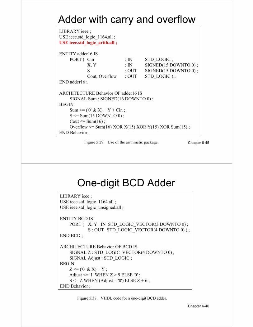
Adder with carry and overflow
Figure 5.28. The 16-bit adder from Figure 5.27 with carry and overflow signals.
Chapter 6-45
Adder with carry and overflowLIBRARY ieee ;
USE ieee.std_logic_1164.all ;
USE ieee.std_logic_arith.all ;
ENTITY adder16 IS
PORT ( Cin : IN STD_LOGIC ;
X, Y : IN SIGNED(15 DOWNTO 0) ;
S : OUT SIGNED(15 DOWNTO 0) ;
Cout, Overflow : OUT STD_LOGIC ) ;
END adder16 ;
ARCHITECTURE Behavior OF adder16 IS
SIGNAL Sum : SIGNED(16 DOWNTO 0) ;
BEGIN
Sum <= ('0' & X) + Y + Cin ;
S <= Sum(15 DOWNTO 0) ;
Cout <= Sum(16) ;
Overflow <= Sum(16) XOR X(15) XOR Y(15) XOR Sum(15) ;
END Behavior ;
Figure 5.29. Use of the arithmetic package.
Chapter 6-46
One-digit BCD AdderLIBRARY ieee ;
USE ieee.std_logic_1164.all ;
USE ieee.std_logic_unsigned.all ;
ENTITY BCD IS
PORT ( X, Y : IN STD_LOGIC_VECTOR(3 DOWNTO 0) ;
S : OUT STD_LOGIC_VECTOR(4 DOWNTO 0) ) ;
END BCD ;
ARCHITECTURE Behavior OF BCD IS
SIGNAL Z : STD_LOGIC_VECTOR(4 DOWNTO 0) ;
SIGNAL Adjust : STD_LOGIC ;
BEGIN
Z <= ('0' & X) + Y ;
Adjust <= '1' WHEN Z > 9 ELSE '0' ;
S <= Z WHEN (Adjust = '0') ELSE Z + 6 ;
END Behavior ;
Figure 5.37. VHDL code for a one-digit BCD adder.
Chapter 6-47
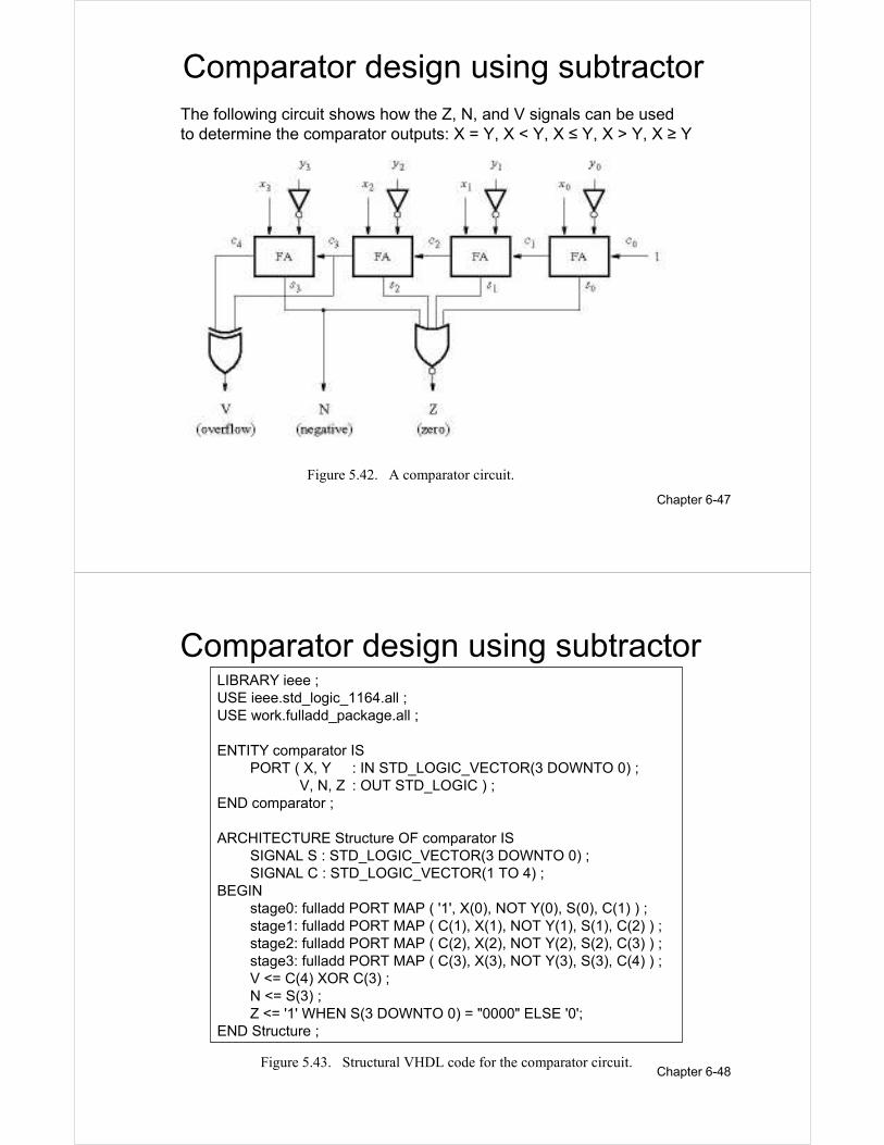
Comparator design using subtractor
The following circuit shows how the Z, N, and V signals can be used
to determine the comparator outputs: X = Y, X < Y, X ≤ Y, X > Y, X ≥ Y
Figure 5.42. A comparator circuit.
Chapter 6-48
Comparator design using subtractorLIBRARY ieee ;
USE ieee.std_logic_1164.all ;
USE work.fulladd_package.all ;
ENTITY comparator IS
PORT ( X, Y : IN STD_LOGIC_VECTOR(3 DOWNTO 0) ;
V, N, Z : OUT STD_LOGIC ) ;
END comparator ;
ARCHITECTURE Structure OF comparator IS
SIGNAL S : STD_LOGIC_VECTOR(3 DOWNTO 0) ;
SIGNAL C : STD_LOGIC_VECTOR(1 TO 4) ;
BEGIN
stage0: fulladd PORT MAP ( '1', X(0), NOT Y(0), S(0), C(1) ) ;
stage1: fulladd PORT MAP ( C(1), X(1), NOT Y(1), S(1), C(2) ) ;
stage2: fulladd PORT MAP ( C(2), X(2), NOT Y(2), S(2), C(3) ) ;
stage3: fulladd PORT MAP ( C(3), X(3), NOT Y(3), S(3), C(4) ) ;
V <= C(4) XOR C(3) ;
N <= S(3) ;
Z <= '1' WHEN S(3 DOWNTO 0) = "0000" ELSE '0';
END Structure ;
Figure 5.43. Structural VHDL code for the comparator circuit.
Chapter 6-49
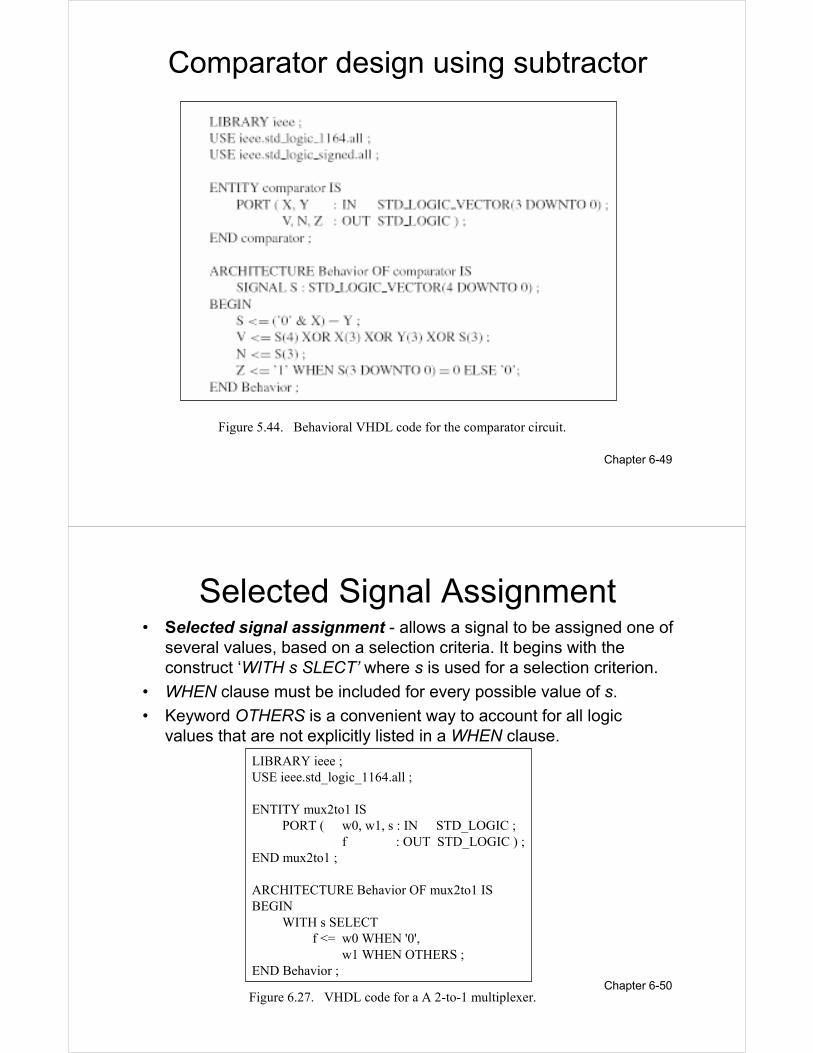
Comparator design using subtractor
Figure 5.44. Behavioral VHDL code for the comparator circuit.
Chapter 6-50
Selected Signal Assignment• Selected signal assignment - allows a signal to be assigned one of
several values, based on a selection criteria. It begins with the
construct ‘WITH s SLECT’ where s is used for a selection criterion.
• WHEN clause must be included for every possible value of s.
• Keyword OTHERS is a convenient way to account for all logic
values that are not explicitly listed in a WHEN clause.
LIBRARY ieee ;
USE ieee.std_logic_1164.all ;
ENTITY mux2to1 IS
PORT ( w0, w1, s : IN STD_LOGIC ;
f : OUT STD_LOGIC ) ;
END mux2to1 ;
ARCHITECTURE Behavior OF mux2to1 IS
BEGIN
WITH s SELECT
f <= w0 WHEN '0',
w1 WHEN OTHERS ;
END Behavior ;
Figure 6.27. VHDL code for a A 2-to-1 multiplexer.
Chapter 6-51
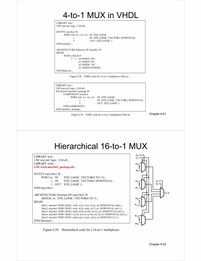
4-to-1 MUX in VHDLLIBRARY ieee ;
USE ieee.std_logic_1164.all ;
ENTITY mux4to1 IS
PORT (w0, w1, w2, w3 : IN STD_LOGIC ;
s : IN STD_LOGIC_VECTOR(1 DOWNTO 0);
f : OUT STD_LOGIC ) ;
END mux4to1 ;
ARCHITECTURE Behavior OF mux4to1 IS
BEGIN
WITH s SELECT
f <= w0 WHEN "00",
w1 WHEN "01",
w2 WHEN "10",
w3 WHEN OTHERS ;
END Behavior ;
LIBRARY ieee ;
USE ieee.std_logic_1164.all ;
PACKAGE mux4to1_package IS
COMPONENT mux4to1
PORT (w0, w1, w2, w3 : IN STD_LOGIC ;
s : IN STD_LOGIC_VECTOR(1 DOWNTO 0) ;
f : OUT STD_LOGIC ) ;
END COMPONENT ;
END mux4to1_package ;
Figure 6.28. VHDL code for a 4-to-1 multiplexer (Part a).
Figure 6.28. VHDL code for a 4-to-1 multiplexer (Part b).
Chapter 6-52
Hierarchical 16-to-1 MUXLIBRARY ieee ;
USE ieee.std_logic_1164.all ;
LIBRARY work ;
USE work.mux4to1_package.all ;
ENTITY mux16to1 IS
PORT (w : IN STD_LOGIC_VECTOR(0 TO 15) ;
s : IN STD_LOGIC_VECTOR(3 DOWNTO 0) ;
f : OUT STD_LOGIC ) ;
END mux16to1 ;
ARCHITECTURE Structure OF mux16to1 IS
SIGNAL m : STD_LOGIC_VECTOR(0 TO 3) ;
BEGIN
Mux1: mux4to1 PORT MAP ( w(0), w(1), w(2), w(3), s(1 DOWNTO 0), m(0) ) ;
Mux2: mux4to1 PORT MAP ( w(4), w(5), w(6), w(7), s(1 DOWNTO 0), m(1) ) ;
Mux3: mux4to1 PORT MAP ( w(8), w(9), w(10), w(11), s(1 DOWNTO 0), m(2) ) ;
Mux4: mux4to1 PORT MAP ( w(12), w(13), w(14), w(15), s(1 DOWNTO 0), m(3) ) ;
Mux5: mux4to1 PORT MAP ( m(0), m(1), m(2), m(3), s(3 DOWNTO 2), f ) ;
END Structure ;
w 8
w 11
s 1
w 0
s 0
w 3
w 4
w 7
w 12
w15
s 3
s 2
f
Figure 6.29. Hierarchical code for a 16-to-1 multiplexer.

Chapter 6-53
2-to-4 binary decoderLIBRARY ieee ;
USE ieee.std_logic_1164.all ;
ENTITY dec2to4 IS
PORT ( w : IN STD_LOGIC_VECTOR(1 DOWNTO 0) ;
En : IN STD_LOGIC ;
y : OUT STD_LOGIC_VECTOR(0 TO 3) ) ;
END dec2to4 ;
ARCHITECTURE Behavior OF dec2to4 IS
SIGNAL Enw : STD_LOGIC_VECTOR(2 DOWNTO 0) ;
BEGIN
Enw <= En & w ; -- use VHDL concatenate (&) operator
WITH Enw SELECT
y <= "1000" WHEN "100",
"0100" WHEN "101",
"0010" WHEN "110",
"0001" WHEN "111",
"0000" WHEN OTHERS ; -- i.e for cases when En=0
END Behavior ;
Figure 6.30. VHDL code for a 2-to-4 binary decoder.
Chapter 6-54
Conditional Signal Assignment• Similar to the selected signal assignment, a conditional signal
assignment allows a signal to be set to one of several values.
• WHEN … ELSE clause is used for conditional signal assignment.
• The priority level associated with each WHEN clause in the
conditional signal assignment is a key difference from the selected
signal assignment, which has no such priority.
LIBRARY ieee ;
USE ieee.std_logic_1164.all ;
ENTITY mux2to1 IS
PORT (w0, w1, s : IN STD_LOGIC ;
f : OUT STD_LOGIC ) ;
END mux2to1 ;
ARCHITECTURE Behavior OF mux2to1 IS
BEGIN
f <= w0 WHEN s = '0' ELSE w1 ;
END Behavior ;
Figure 6.31. A 2-to-1 multiplexer using a conditional signal assignment.

Chapter 6-55
4-to-2 priority encoder
d001
010
w0 y1
d
y0
1 1
01
1
11
z
1xx
0
x
w1
01x
0
x
w2
001
0
x
w3
000
0
1
LIBRARY ieee ;
USE ieee.std_logic_1164.all ;
ENTITY priority IS
PORT ( w : IN STD_LOGIC_VECTOR(3 DOWNTO 0) ;
y : OUT STD_LOGIC_VECTOR(1 DOWNTO 0) ;
z : OUT STD_LOGIC ) ;
END priority ;
ARCHITECTURE Behavior OF priority IS
BEGIN
y <= "11" WHEN w(3) = '1' ELSE
"10" WHEN w(2) = '1' ELSE
"01" WHEN w(1) = '1' ELSE
"00" ;
z <= '0' WHEN w = "0000" ELSE '1' ;
END Behavior ;
Figure 6.32. VHDL code for a priority encoder.
Chapter 6-56
LIBRARY ieee ;
USE ieee.std_logic_1164.all ;
ENTITY priority IS
PORT ( w : IN STD_LOGIC_VECTOR(3 DOWNTO 0) ;
y : OUT STD_LOGIC_VECTOR(1 DOWNTO 0) ;
z : OUT STD_LOGIC ) ;
END priority ;
ARCHITECTURE Behavior OF priority IS
BEGIN
WITH w SELECT
y <= "00" WHEN "0001",
"01" WHEN "0010",
"01" WHEN "0011",
"10" WHEN "0100",
"10" WHEN "0101",
"10" WHEN "0110",
"10" WHEN "0111",
"11" WHEN OTHERS ;
WITH w SELECT
z <= '0' WHEN "0000",
'1' WHEN OTHERS ;
END Behavior ;
Figure 6.33. Less efficient code for a priority encoder.

Chapter 6-57
Comparator using relational operator• Use the package named std_logic_unsigned to allow the use of
relational operators on UNSIGNED binary numbers.
• Alternately, we can use the package named std_logic_arith for
both UNSIGNED and SIGNED data types.
• The VHDL compiler instantiates a predefined module to implement
each of the comparison operations.
LIBRARY ieee ;
USE ieee.std_logic_1164.all ;
USE ieee.std_logic_unsigned.all ;
ENTITY compare IS
PORT (A, B : IN STD_LOGIC_VECTOR(3 DOWNTO 0) ;
AeqB, AgtB, AltB : OUT STD_LOGIC ) ;
END compare ;
ARCHITECTURE Behavior OF compare IS
BEGIN
AeqB <= '1' WHEN A = B ELSE '0' ;
AgtB <= '1' WHEN A > B ELSE '0' ;
AltB <= '1' WHEN A < B ELSE '0' ;
END Behavior ;
LIBRARY ieee ;
USE ieee.std_logic_1164.all ;
USE ieee.std_logic_arith.all ;
ENTITY compare IS
PORT (A, B : IN SIGNED(3 DOWNTO 0) ;
AeqB, AgtB, AltB : OUT STD_LOGIC ) ;
END compare ;
ARCHITECTURE Behavior OF compare IS
BEGIN
AeqB <= '1' WHEN A = B ELSE '0' ;
AgtB <= '1' WHEN A > B ELSE '0' ;
AltB <= '1' WHEN A < B ELSE '0' ;
END Behavior ;
Figure 6.34. VHDL code for a four-bit
comparator.
Figure 6.35. The code from Figure 6.34 for
signed numbers.
Chapter 6-58
Generate Statements• VHDL provides the ‘FOR GENERATE’ and ‘IF GENERATE’
statements for describing regularly structured hierarchical code.
LIBRARY ieee ;
USE ieee.std_logic_1164.all ;
USE work.mux4to1_package.all ;
ENTITY mux16to1 IS
PORT ( w : IN STD_LOGIC_VECTOR(0 TO 15) ;
s : IN STD_LOGIC_VECTOR(3 DOWNTO 0) ;
f : OUT STD_LOGIC ) ;
END mux16to1 ;
ARCHITECTURE Structure OF mux16to1 IS
SIGNAL m : STD_LOGIC_VECTOR(0 TO 3) ;
BEGIN
G1: FOR i IN 0 TO 3 GENERATE
Muxes: mux4to1 PORT MAP (
w(4*i), w(4*i+1), w(4*i+2), w(4*i+3), s(1 DOWNTO 0), m(i) ) ;
END GENERATE ;
Mux5: mux4to1 PORT MAP ( m(0), m(1), m(2), m(3), s(3 DOWNTO 2), f ) ;
END Structure ;
Figure 6.36. Code for a 16-to-1 multiplexer using a generate statement.

Chapter 6-59
LIBRARY ieee ;
USE ieee.std_logic_1164.all ;
ENTITY dec4to16 IS
PORT ( w : IN STD_LOGIC_VECTOR(3 DOWNTO 0) ;
En : IN STD_LOGIC ;
y : OUT STD_LOGIC_VECTOR(0 TO 15) ) ;
END dec4to16 ;
ARCHITECTURE Structure OF dec4to16 IS
COMPONENT dec2to4
PORT ( w : IN STD_LOGIC_VECTOR(1 DOWNTO 0) ;
En : IN STD_LOGIC ;
y : OUT STD_LOGIC_VECTOR(0 TO 3) ) ;
END COMPONENT ;
SIGNAL m : STD_LOGIC_VECTOR(0 TO 3) ;
BEGIN
G1: FOR i IN 0 TO 3 GENERATE
Dec_ri: dec2to4 PORT MAP ( w(1 DOWNTO 0), m(i), y(4*i TO 4*i+3) );
G2: IF i=3 GENERATE
Dec_left: dec2to4 PORT MAP ( w(i DOWNTO i-1), En, m ) ;
END GENERATE ;
END GENERATE ;
END Structure ;
Figure 6.37. Hierarchical code for a 4-to-16 binary decoder (see Fig 6.18 and 6.30)
Chapter 6-60
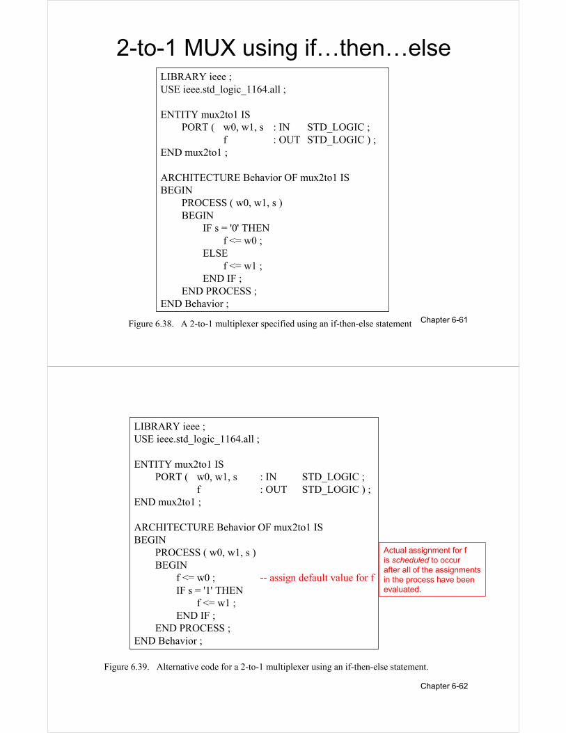
Concurrent vs. Sequential
Assignment Statements• Concurrent assignment statements – has the property that the order in which they
appear in VHDL code does not affect the meaning of the code. Examples of such statements:– Simple assignment statements (for logic or arithmetic expressions)
– Selected assignment statements
– Conditional assignment statements
• Sequential assignment statements – the ordering of the statements may affect the meaning of the code. Examples:– IF … THEN … ELSE statement
– CASE statement
• VHDL requires that sequential assignment statements be placed inside processstatement, that begins with the PROCESS keyword followed by a parenthesized list of signals, called sensitivity list.– For a combinational circuit the sensitivity list includes all input signals that are used inside the
process.
– When there is a change in the value of any signal in the process’s sensitivity list the process becomes active. Once active the statements inside the process are evaluated in sequential order.
– Any assignment made to signals inside the process are not visible outside the process until all of statements in the process have been evaluated.
– If there are multiple assignments to the same signal, only the last one has any visible effect.
– While statements in a process are sequential, the process statement itself is a concurrent statement.
– A process statement is translated by the VHDL compiler into logic equations.
Chapter 6-61
2-to-1 MUX using if…then…elseLIBRARY ieee ;
USE ieee.std_logic_1164.all ;
ENTITY mux2to1 IS
PORT ( w0, w1, s : IN STD_LOGIC ;
f : OUT STD_LOGIC ) ;
END mux2to1 ;
ARCHITECTURE Behavior OF mux2to1 IS
BEGIN
PROCESS ( w0, w1, s )
BEGIN
IF s = '0' THEN
f <= w0 ;
ELSE
f <= w1 ;
END IF ;
END PROCESS ;
END Behavior ;
Figure 6.38. A 2-to-1 multiplexer specified using an if-then-else statement
Chapter 6-62
LIBRARY ieee ;
USE ieee.std_logic_1164.all ;
ENTITY mux2to1 IS
PORT ( w0, w1, s : IN STD_LOGIC ;
f : OUT STD_LOGIC ) ;
END mux2to1 ;
ARCHITECTURE Behavior OF mux2to1 IS
BEGIN
PROCESS ( w0, w1, s )
BEGIN
f <= w0 ; -- assign default value for f
IF s = '1' THEN
f <= w1 ;
END IF ;
END PROCESS ;
END Behavior ;
Figure 6.39. Alternative code for a 2-to-1 multiplexer using an if-then-else statement.
Actual assignment for f
is scheduled to occur
after all of the assignments
in the process have been
evaluated.
Chapter 6-63
Priority encoder using if…then…elseLIBRARY ieee ;
USE ieee.std_logic_1164.all ;
ENTITY priority IS
PORT (w : IN STD_LOGIC_VECTOR(3 DOWNTO 0) ;
y : OUT STD_LOGIC_VECTOR(1 DOWNTO 0) ;
z : OUT STD_LOGIC ) ;
END priority ;
ARCHITECTURE Behavior OF priority IS
BEGIN
PROCESS ( w )
BEGIN
IF w(3) = '1' THEN
y <= "11" ;
ELSIF w(2) = '1' THEN
y <= "10" ;
ELSIF w(1) = '1' THEN
y <= "01" ;
ELSE
y <= "00" ;
END IF ;
END PROCESS ;
z <= '0' WHEN w = "0000" ELSE '1' ;
END Behavior ;
Figure 6.40. A priority encoder specified using the if-then-else statement.
VHDL syntax does not allow
conditional assignment
statement or selected
assignment statement to
appear inside a process.
Chapter 6-64
LIBRARY ieee ;
USE ieee.std_logic_1164.all ;
ENTITY priority IS
PORT ( w : IN STD_LOGIC_VECTOR(3 DOWNTO 0) ;
y : OUT STD_LOGIC_VECTOR(1 DOWNTO 0) ;
z : OUT STD_LOGIC ) ;
END priority ;
ARCHITECTURE Behavior OF priority IS
BEGIN
PROCESS ( w )
BEGIN
y <= "00" ;
IF w(1) = '1' THEN y <= "01" ; END IF ;
IF w(2) = '1' THEN y <= "10" ; END IF ;
IF w(3) = '1' THEN y <= "11" ; END IF ;
z <= '1' ;
IF w = "0000" THEN z <= '0' ; END IF ;
END PROCESS ;
END Behavior ;
Figure 6.41. Alternative code for the priority encoder.
Chapter 6-65
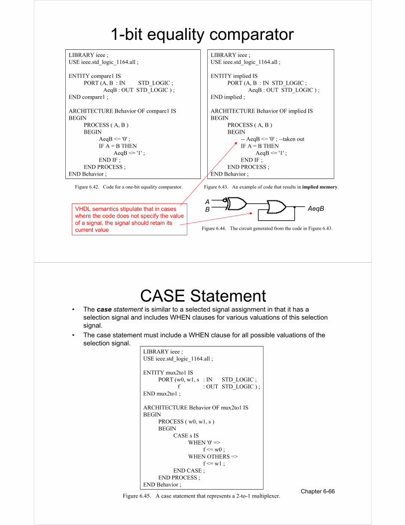
1-bit equality comparatorLIBRARY ieee ;
USE ieee.std_logic_1164.all ;
ENTITY compare1 IS
PORT (A, B : IN STD_LOGIC ;
AeqB : OUT STD_LOGIC ) ;
END compare1 ;
ARCHITECTURE Behavior OF compare1 IS
BEGIN
PROCESS ( A, B )
BEGIN
AeqB <= '0' ;
IF A = B THEN
AeqB <= '1' ;
END IF ;
END PROCESS ;
END Behavior ;
LIBRARY ieee ;
USE ieee.std_logic_1164.all ;
ENTITY implied IS
PORT (A, B : IN STD_LOGIC ;
AeqB : OUT STD_LOGIC ) ;
END implied ;
ARCHITECTURE Behavior OF implied IS
BEGIN
PROCESS ( A, B )
BEGIN
-- AeqB <= '0' ; --taken out
IF A = B THEN
AeqB <= '1' ;
END IF ;
END PROCESS ;
END Behavior ;
Figure 6.42. Code for a one-bit equality comparator. Figure 6.43. An example of code that results in implied memory.
A B AeqB
Figure 6.44. The circuit generated from the code in Figure 6.43.
VHDL semantics stipulate that in cases
where the code does not specify the value
of a signal, the signal should retain its
current value
Chapter 6-66
CASE Statement• The case statement is similar to a selected signal assignment in that it has a
selection signal and includes WHEN clauses for various valuations of this selection
signal.
• The case statement must include a WHEN clause for all possible valuations of the
selection signal.
LIBRARY ieee ;
USE ieee.std_logic_1164.all ;
ENTITY mux2to1 IS
PORT (w0, w1, s : IN STD_LOGIC ;
f : OUT STD_LOGIC ) ;
END mux2to1 ;
ARCHITECTURE Behavior OF mux2to1 IS
BEGIN
PROCESS ( w0, w1, s )
BEGIN
CASE s IS
WHEN '0' =>
f <= w0 ;
WHEN OTHERS =>
f <= w1 ;
END CASE ;
END PROCESS ;
END Behavior ;
Figure 6.45. A case statement that represents a 2-to-1 multiplexer.

Chapter 6-67
Process for 2-to-4 binary decoderLIBRARY ieee ;
USE ieee.std_logic_1164.all ;
ENTITY dec2to4 IS
PORT ( w : IN STD_LOGIC_VECTOR(1 DOWNTO 0) ;
En : IN STD_LOGIC ;
y : OUT STD_LOGIC_VECTOR(0 TO 3) ) ;
END dec2to4 ;
ARCHITECTURE Behavior OF dec2to4 IS
BEGIN
PROCESS ( w, En )
BEGIN
IF En = '1' THEN
CASE w IS
WHEN "00" => y <= "1000" ;
WHEN "01" => y <= "0100" ;
WHEN "10" => y <= "0010" ;
WHEN OTHERS => y <= "0001" ;
END CASE ;
ELSE
y <= "0000" ;
END IF ;
END PROCESS ;
END Behavior ;
Figure 6.46. A process statement that describes a 2-to-4 binary decoder.
Chapter 6-68
BCD-to7-segment decoderLIBRARY ieee ;
USE ieee.std_logic_1164.all ;
ENTITY seg7 IS
PORT (bcd : IN STD_LOGIC_VECTOR(3 DOWNTO 0) ;
leds : OUT STD_LOGIC_VECTOR(1 TO 7) ) ;
END seg7 ;
ARCHITECTURE Behavior OF seg7 IS
BEGIN
PROCESS ( bcd )
BEGIN
CASE bcd IS -- abcdefg
WHEN "0000" => leds <= "1111110" ;
WHEN "0001" => leds <= "0110000" ;
WHEN "0010" => leds <= "1101101" ;
WHEN "0011" => leds <= "1111001" ;
WHEN "0100" => leds <= "0110011" ;
WHEN "0101" => leds <= "1011011" ;
WHEN "0110" => leds <= "1011111" ;
WHEN "0111" => leds <= "1110000" ;
WHEN "1000" => leds <= "1111111" ;
WHEN "1001" => leds <= "1110011" ;
WHEN OTHERS => leds <= "-------" ;
END CASE ;
END PROCESS ;
END Behavior ;
Figure 6.47. Code that represents a BCD-to-7-segment decoder
w 0
a
w 1
b c d w 2
w 3 e f g
c e
a
g
b f
d
1
0
1
1
1
1
1
w 0 a
1
b
0 1
1
1
1
0
1
1
0
1
0
0
w 1
0
1
1
0
0
w 2
0
0
0
0
1
w 3
0
0
0
0
0
c
1
0
1
0
0
1
1
0
1
1
1
0
0
0
0
1
1 0 0 1
1
1
1
1
0
1
1
0
1 1
1
1
1
1
1
0
1
1
1
d
0
1
0
0
1
0
e
1
0
1
1
1
0
1
0
0
1
0
0
0
1
f
1
0
0
1
1
1
g
1
0
1
1
1
1
1
1
0
1
Figure 6.25. A BCD-to-7-segment
display code converter.
Chapter 6-69
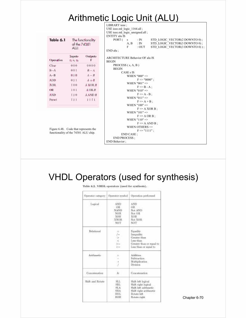
Arithmetic Logic Unit (ALU)LIBRARY ieee ;
USE ieee.std_logic_1164.all ;
USE ieee.std_logic_unsigned.all ;
ENTITY alu IS
PORT ( s : IN STD_LOGIC_VECTOR(2 DOWNTO 0) ;
A, B : IN STD_LOGIC_VECTOR(3 DOWNTO 0) ;
F : OUT STD_LOGIC_VECTOR(3 DOWNTO 0) ) ;
END alu ;
ARCHITECTURE Behavior OF alu IS
BEGIN
PROCESS ( s, A, B )
BEGIN
CASE s IS
WHEN "000" =>
F <= "0000" ;
WHEN "001" =>
F <= B - A ;
WHEN "010" =>
F <= A - B ;
WHEN "011" =>
F <= A + B ;
WHEN "100" =>
F <= A XOR B ;
WHEN "101" =>
F <= A OR B ;
WHEN "110" =>
F <= A AND B ;
WHEN OTHERS =>
F <= "1111" ;
END CASE ;
END PROCESS ;
END Behavior ;
Figure 6.48. Code that represents the
functionality of the 74381 ALU chip.
Chapter 6-70
VHDL Operators (used for synthesis)