Combinational and Sequential Circuit Design
75
Sequential Logic Circuits VLSI Design Page 3. 1 UNIT III SEQUENTIAL LOGIC CIRCUITS Static and Dynamic Latches and Registers, Timing issues, pipelines, clock strategies, Memory architecture and memory control circuits, Low power memory circuits, Synchronous and synchronous design. 3.5.SYNCHRONIZER Sequencing elements are characterized by their setup and hold time. If the data input changes before the setup time, the output reflects the new value after a bounded propagation delay. If the data changes after the hold time, the output reflects the old value after a bounded propagation delay. If the data changes during the aperture between the setup and hold times, the output may be unpredictable and the time for the output to settle to a good logic level may be unbounded. A synchronizer is a circuit that accepts an input that can change at arbitrary times and produces an output aligned to the synchronizer’s clock. Because the input can change during the synchronizer’s aperture, the synchronizer has a nonzero probability of producing a metastable output. 3.5.1 Metastability A latch is a bistable device; i.e., it has two stable states (0 and 1). Under the right conditions, that latch can enter a metastable state in which the output is at an indeterminate level between 0 and 1. Fig 5.1 Metastable state in static latch For example, Figure 5.1 shows a simple model for a static latch consisting of two switches and two inverters. While the latch is transparent, the sample switch is closed and the hold switch open (Figure 5.1 (a)). When the latch goes opaque, the sample switch opens and the hold switch closes (Figure 4.1 (b)). Figure 5.1(c) shows the DC transfer characteristics of the www.AllAbtEngg.com AllAbtEngg Android Application for Anna University, Polytechnic & School
Transcript of Combinational and Sequential Circuit Design
Sequential Logic Circuits
VLSI Design Page 3. 1
UNIT III SEQUENTIAL LOGIC CIRCUITS
Static and Dynamic Latches and Registers, Timing issues, pipelines, clock strategies, Memory
architecture and memory control circuits, Low power memory circuits, Synchronous and
synchronous design.
3.5.SYNCHRONIZER
Sequencing elements are characterized by their setup and hold time. If the data input
changes before the setup time, the output reflects the new value after a bounded propagation
delay. If the data changes after the hold time, the output reflects the old value after a bounded
propagation delay. If the data changes during the aperture between the setup and hold times, the
output may be unpredictable and the time for the output to settle to a good logic level may be
unbounded.
A synchronizer is a circuit that accepts an input that can change at arbitrary times and
produces an output aligned to the synchronizer’s clock. Because the input can change during the
synchronizer’s aperture, the synchronizer has a nonzero probability of producing a metastable
output.
3.5.1 Metastability
A latch is a bistable device; i.e., it has two stable states (0 and 1). Under the right
conditions, that latch can enter a metastable state in which the output is at an indeterminate
level between 0 and 1.
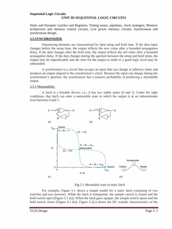
Fig 5.1 Metastable state in static latch
For example, Figure 5.1 shows a simple model for a static latch consisting of two
switches and two inverters. While the latch is transparent, the sample switch is closed and the
hold switch open (Figure 5.1 (a)). When the latch goes opaque, the sample switch opens and the
hold switch closes (Figure 4.1 (b)). Figure 5.1(c) shows the DC transfer characteristics of the
www.AllAbtEngg.com
AllAbtEngg Android Application for Anna University, Polytechnic & School
Sequential Logic Circuits
VLSI Design Page 3. 2
two inverters. Because A =B when the latch is opaque, the stable states are A =B =0 and A =B
=VDD. The metastable state is A=B =Vm, where Vm is an invalid logic level. This point is
called metastable because the voltages are self-consistent and can remain there indefinitely.
However, any noise or other disturbance will cause A and B to switch to one of the two stable
states. Figure 5.1 (d) shows an analogy of a ball delicately balanced on a hill. The top of the hill
is a metastable state. Any disturbance will cause the ball to roll down to one of the two stable
states on the left or right side of the hill.
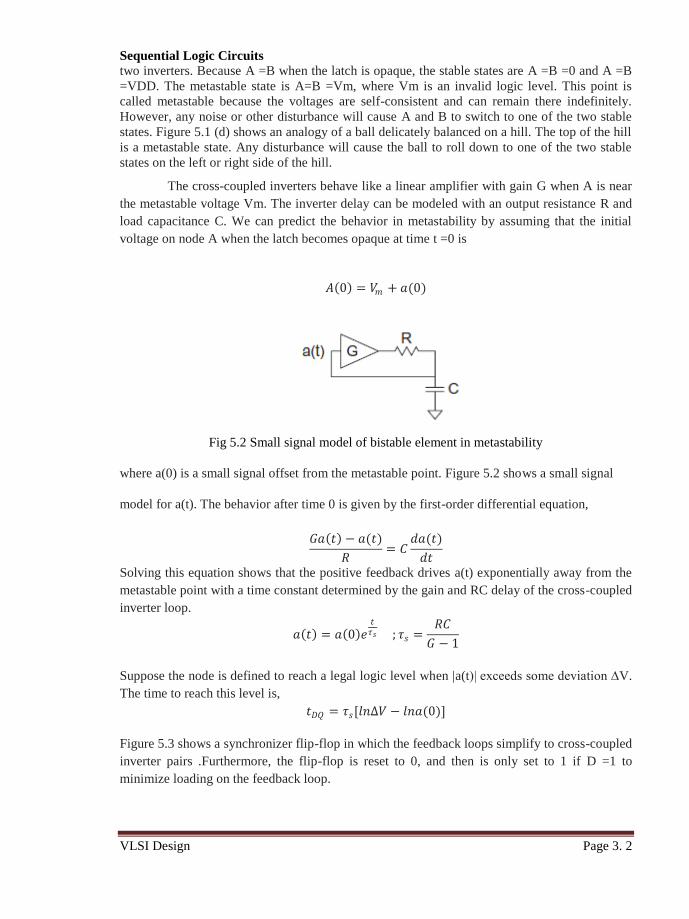
The cross-coupled inverters behave like a linear amplifier with gain G when A is near
the metastable voltage Vm. The inverter delay can be modeled with an output resistance R and
load capacitance C. We can predict the behavior in metastability by assuming that the initial
voltage on node A when the latch becomes opaque at time t =0 is
𝐴 0 = 𝑉𝑚 + 𝑎(0)
Fig 5.2 Small signal model of bistable element in metastability
where a(0) is a small signal offset from the metastable point. Figure 5.2 shows a small signal
model for a(t). The behavior after time 0 is given by the first-order differential equation,
𝐺𝑎 𝑡 − 𝑎(𝑡)
𝑅= 𝐶
𝑑𝑎(𝑡)
𝑑𝑡
Solving this equation shows that the positive feedback drives a(t) exponentially away from the
metastable point with a time constant determined by the gain and RC delay of the cross-coupled
inverter loop.
𝑎 𝑡 = 𝑎 0 𝑒𝑡𝜏𝑠 ; 𝜏𝑠 =
𝑅𝐶
𝐺 − 1
Suppose the node is defined to reach a legal logic level when |a(t)| exceeds some deviation ∆V.
The time to reach this level is,
𝑡𝐷𝑄 = 𝜏𝑠[𝑙𝑛∆𝑉 − 𝑙𝑛𝑎(0)]
Figure 5.3 shows a synchronizer flip-flop in which the feedback loops simplify to cross-coupled
inverter pairs .Furthermore, the flip-flop is reset to 0, and then is only set to 1 if D =1 to
minimize loading on the feedback loop.
www.AllAbtEngg.com
AllAbtEngg Android Application for Anna University, Polytechnic & School

Sequential Logic Circuits
VLSI Design Page 3. 3
Fig 5.3 Fast synchronizer flip-flop
The flip-flop consists of master and slave jamb latches. Each latch is reset to 0 while D
=0. When D rises before φ, the master output X is driven high. This in turn drives the slave
output Q high when φ rises. The pulldown transistors are just large enough to overpower the
cross-coupled inverters, but should add as little stray capacitance to the feedback loops as
possible. X and Q are buffered with small inverters so they do not load the feedback loops.
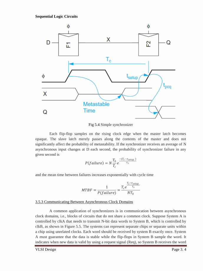
3.5.2 A Simple Synchronizer
A synchronizer accepts an input D and a clock ɸ. It produces an output Q that ought to
be valid some bounded delay after the clock. The synchronizer has an aperture defined by a
setup and hold time around the rising edge of the clock. If the data is stable during the aperture,
Q should equal D. If the data changes during the aperture, Q can be chosen arbitrarily.
Unfortunately, it is impossible to build a perfect synchronizer because the duration of
metastability can be unbounded. We define synchronizer failure as occurring if the output has
not settled to a valid logic level after some time t .Figure 5.4 shows a simple synchronizer built
from a pair of flip-flops. F1 samples the asynchronous input D. The output X may be
metastable for some time, but will settle to a good level with high probability if we wait long
enough. F2 samples X and produces an output Q that should be a valid logic level and be
aligned with the clock. The synchronizer has a latency of one clock cycle, Tc . It can fail if X
has not settled to a valid level by a setup time before the second clock edge.
www.AllAbtEngg.com
AllAbtEngg Android Application for Anna University, Polytechnic & School
Sequential Logic Circuits
VLSI Design Page 3. 4
Fig 5.4 Simple synchronizer
Each flip-flop samples on the rising clock edge when the master latch becomes
opaque. The slave latch merely passes along the contents of the master and does not
significantly affect the probability of metastability. If the synchronizer receives an average of N
asynchronous input changes at D each second, the probability of synchronizer failure in any
given second is
𝑃 𝑓𝑎𝑖𝑙𝑢𝑟𝑒 = 𝑁𝑇0
𝑇𝑐𝑒−(𝑇𝑐−𝑡𝑠𝑒𝑡𝑢𝑝 )
𝜏𝑠
and the mean time between failures increases exponentially with cycle time
𝑀𝑇𝐵𝐹 =1
𝑃(𝑓𝑎𝑖𝑙𝑢𝑟𝑒)=
𝑇𝑐𝑒𝑇𝑐−𝑡𝑠𝑒𝑡𝑢𝑝
𝜏𝑠
𝑁𝑇0
3.5.3 Communicating Between Asynchronous Clock Domains
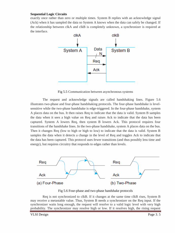
A common application of synchronizers is in communication between asynchronous
clock domains, i.e., blocks of circuits that do not share a common clock. Suppose System A is
controlled by clkA that needs to transmit N-bit data words to System B, which is controlled by
clkB, as shown in Figure 5.5. The systems can represent separate chips or separate units within
a chip using unrelated clocks. Each word should be received by system B exactly once. System
A must guarantee that the data is stable while the flip-flops in System B sample the word. It
indicates when new data is valid by using a request signal (Req), so System B receives the word
www.AllAbtEngg.com
AllAbtEngg Android Application for Anna University, Polytechnic & School
Sequential Logic Circuits
VLSI Design Page 3. 5
exactly once rather than zero or multiple times. System B replies with an acknowledge signal
(Ack) when it has sampled the data so System A knows when the data can safely be changed. If
the relationship between clkA and clkB is completely unknown, a synchronizer is required at
the interface.
Fig 5.5 Communication between asynchronous systems
The request and acknowledge signals are called handshaking lines. Figure 5.6
illustrates two-phase and four-phase handshaking protocols. The four-phase handshake is level-
sensitive while the two-phase handshake is edge-triggered. In the four-phase handshake, system
A places data on the bus. It then raises Req to indicate that the data is valid. System B samples
the data when it sees a high value on Req and raises Ack to indicate that the data has been
captured. System A lowers Req, then system B lowers Ack. This protocol requires four
transitions of the handshake lines. In the two-phase handshake, system A places data on the bus.
Then it changes Req (low to high or high to low) to indicate that the data is valid. System B
samples the data when it detects a change in the level of Req and toggles Ack to indicate that
the data has been captured. This protocol uses fewer transitions (and thus possibly less time and
energy), but requires circuitry that responds to edges rather than levels.
Fig 5.6 Four-phase and two-phase handshake protocols
Req is not synchronized to clkB. If it changes at the same time clkB rises, System B
may receive a metastable value. Thus, System B needs a synchronizer on the Req input. If the
synchronizer waits long enough, the request will resolve to a valid logic level with very high
probability. The synchronizer may resolve high or low. If it resolves high, the rising request
www.AllAbtEngg.com
AllAbtEngg Android Application for Anna University, Polytechnic & School
Sequential Logic Circuits
VLSI Design Page 3. 6
was detected and System B can sample the data. If it resolves low, the rising request was just
missed. However, it will be detected on the next cycle of clkB, just as it would have been if the
rising request occurred just slightly later. Ack is not synchronized to clkA, so it also requires a
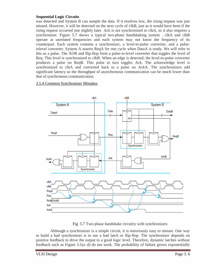
synchronizer. Figure 5.7 shows a typical two-phase handshaking system . clkA and clkB
operate at unrelated frequencies and each system may not know the frequency of its
counterpart. Each system contains a synchronizer, a level-to-pulse converter, and a pulse-
tolevel converter. System A asserts ReqA for one cycle when DataA is ready. We will refer to
this as a pulse. The XOR and flip-flop form a pulse-to-level converter that toggles the level of
Req. This level is synchronized to clkB. When an edge is detected, the level-to-pulse converter
produces a pulse on ReqB. This pulse in turn toggles Ack. The acknowledge level is
synchronized to clkA and converted back to a pulse on AckA. The synchronizers add
significant latency so the throughput of asynchronous communication can be much lower than
that of synchronous communication.
3.5.4 Common Synchronizer Mistakes
Fig 5.7 Two-phase handshake circuitry with synchronizers
Although a synchronizer is a simple circuit, it is notoriously easy to misuse. One way
to build a bad synchronizer is to use a bad latch or flip-flop. The synchronizer depends on
positive feedback to drive the output to a good logic level. Therefore, dynamic latches without
feedback such as Figure 3.1(a–d) do not work. The probability of failure grows exponentially
www.AllAbtEngg.com
AllAbtEngg Android Application for Anna University, Polytechnic & School
Sequential Logic Circuits
VLSI Design Page 3. 7
with the time constant of the feedback loop. Therefore, the loop should be lightly loaded. The
latch from Figure 3.1(f ) is a poor choice because a large capacitive load on the output will
increase the time constant; Figure 3.1(g) is a much better choice.
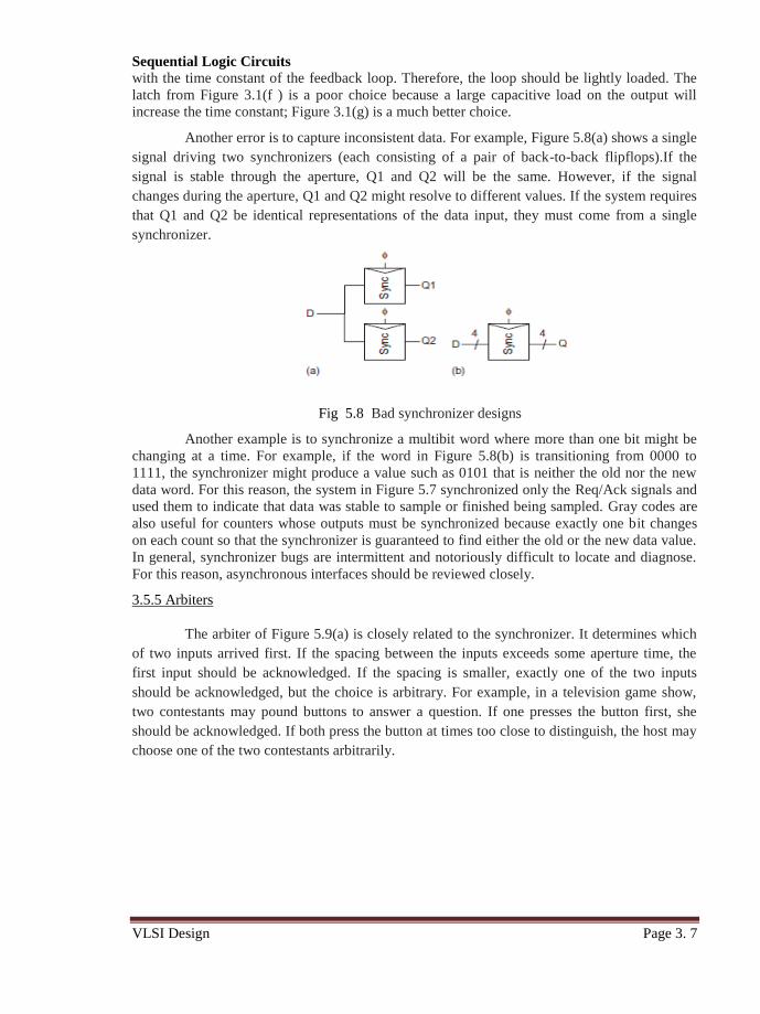
Another error is to capture inconsistent data. For example, Figure 5.8(a) shows a single
signal driving two synchronizers (each consisting of a pair of back-to-back flipflops).If the
signal is stable through the aperture, Q1 and Q2 will be the same. However, if the signal
changes during the aperture, Q1 and Q2 might resolve to different values. If the system requires
that Q1 and Q2 be identical representations of the data input, they must come from a single
synchronizer.
Fig 5.8 Bad synchronizer designs
Another example is to synchronize a multibit word where more than one bit might be
changing at a time. For example, if the word in Figure 5.8(b) is transitioning from 0000 to
1111, the synchronizer might produce a value such as 0101 that is neither the old nor the new
data word. For this reason, the system in Figure 5.7 synchronized only the Req/Ack signals and
used them to indicate that data was stable to sample or finished being sampled. Gray codes are
also useful for counters whose outputs must be synchronized because exactly one bit changes
on each count so that the synchronizer is guaranteed to find either the old or the new data value.
In general, synchronizer bugs are intermittent and notoriously difficult to locate and diagnose.
For this reason, asynchronous interfaces should be reviewed closely.
3.5.5 Arbiters
The arbiter of Figure 5.9(a) is closely related to the synchronizer. It determines which
of two inputs arrived first. If the spacing between the inputs exceeds some aperture time, the
first input should be acknowledged. If the spacing is smaller, exactly one of the two inputs
should be acknowledged, but the choice is arbitrary. For example, in a television game show,
two contestants may pound buttons to answer a question. If one presses the button first, she
should be acknowledged. If both press the button at times too close to distinguish, the host may
choose one of the two contestants arbitrarily.
www.AllAbtEngg.com
AllAbtEngg Android Application for Anna University, Polytechnic & School

Sequential Logic Circuits
VLSI Design Page 3. 8
Fig 5.9 Arbiter
Figure 5.9(b) shows an arbiter built from an SR latch and a four-transistor
metastability filter. If one of the request inputs arrives well before the other, the latch will
respond appropriately. However, if they arrive at nearly the same time, the latch may be driven
into metastability, as shown in Figure 5.9(c). The filter keeps both acknowledge signals low
until the voltage difference between the internal nodes n1 and n2 exceeds Vt , indicating that a
decision has been made. Such an asynchronous arbiter will never produce metastable outputs.
However, the time required to make the decision can be unbounded, so the acknowledge signals
must be synchronized before they are used in a clocked system. Arbiters can be generalized to
select 1-of-N or M-of-N inputs. However, such arbiters have multiple metastable states and
require careful design.
3.6 Static Latches and Registers:
Figure 7.1 shows a block diagram of a generic finite state machine (FSM) that consists
of combinational logic and registers, which hold the system state. The system depicted here
belongs to the class of synchronous sequential systems, in which all registers are under control
of a single global clock. The outputs of the FSM are a function of the current Inputs and the
Current State. The Next State is determined based on the Current State and the current Inputs
and is fed to the inputs of registers. On the rising edge of the clock, the Next State bits are
copied to the outputs of the registers (after some propagation delay), and a new cycle begins.
The register then ignores changes in the input signals until the next rising edge. In general,
registers can be positive edge-triggered (where the input data is copied on the positive edge of
the clock) or negative edge-triggered (where the input data is copied on the negative edge, as is
indicated by a small circle at the clock input)
www.AllAbtEngg.com
AllAbtEngg Android Application for Anna University, Polytechnic & School

Sequential Logic Circuits
VLSI Design Page 3. 9
A variety of choices in sequential primitives and clocking methodologies exist; making
the correct selection is getting increasingly important in modern digital circuits, and can have a
great impact on performance, power, and/or design complexity.
7.2.1 The Bistability Principle
Static memories use positive feedback to create a bistable circuit a circuit having two
stable states that represent 0 and 1. The basic idea is shown in Figure 7.4a, which shows two
inverters connected in cascade along with a voltage-transfer characteristic typical of such a
circuit. Also plotted are the VTCs of the first inverter, that is, Vo1 versus Vi1, and the second
inverter (Vo2 versus Vo1). The latter plot is rotated to accentuate that Vi2 = Vo1. Assume now
that the output of the second inverter Vo2 is connected to the input of the first Vi1, as shown by
the dotted lines in Figure 7.4a. The resulting circuit has only three possible operation points (A,
B, and C), as demonstrated on the combined VTC. The following important conjecture is easily
proven to be valid:
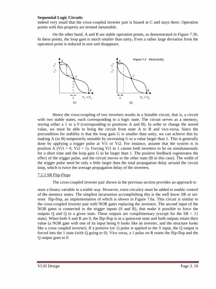
Suppose that the cross-coupled inverter pair is biased at point C. A small deviation
from this bias point, possibly caused by noise, is amplified and regenerated around the circuit
loop. This is a consequence of the gain around the loop being larger than 1. The effect is
demonstrated in Figure 7.5a. A small deviation δ is applied to Vi1 (biased in C). This deviation
is amplified by the gain of the inverter. The enlarged divergence is applied to the second
inverter and amplified once more. The bias point moves away from C until one of the operation
points A or B is reached. In conclusion, C is an unstable operation point. Every deviation (even
the smallest one) causes the operation point to run away from its original bias. The chance is
www.AllAbtEngg.com
AllAbtEngg Android Application for Anna University, Polytechnic & School
Sequential Logic Circuits
VLSI Design Page 3. 10
indeed very small that the cross-coupled inverter pair is biased at C and stays there. Operation
points with this property are termed metastable.
On the other hand, A and B are stable operation points, as demonstrated in Figure 7.5b.
In these points, the loop gain is much smaller than unity. Even a rather large deviation from the
operation point is reduced in size and disappears.
Hence the cross-coupling of two inverters results in a bistable circuit, that is, a circuit
with two stable states, each corresponding to a logic state. The circuit serves as a memory,
storing either a 1 or a 0 (corresponding to positions A and B). In order to change the stored
value, we must be able to bring the circuit from state A to B and vice-versa. Since the
precondition for stability is that the loop gain G is smaller than unity, we can achieve this by
making A (or B) temporarily unstable by increasing G to a value larger than 1. This is generally
done by applying a trigger pulse at Vi1 or Vi2. For instance, assume that the system is in
position A (Vi1 = 0, Vi2 = 1). Forcing Vi1 to 1 causes both inverters to be on simultaneously
for a short time and the loop gain G to be larger than 1. The positive feedback regenerates the
effect of the trigger pulse, and the circuit moves to the other state (B in this case). The width of
the trigger pulse need be only a little larger than the total propagation delay around the circuit
loop, which is twice the average propagation delay of the inverters.
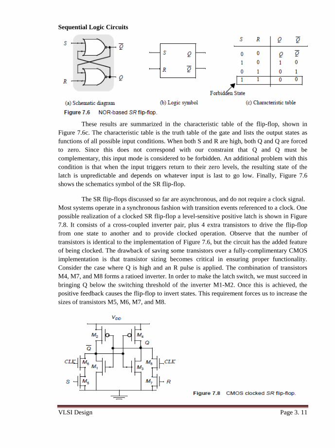
7.2.2 SR Flip-Flops
The cross-coupled inverter pair shown in the previous section provides an approach to
store a binary variable in a stable way. However, extra circuitry must be added to enable control
of the memory states. The simplest incarnation accomplishing this is the well know SR or set-
reset flip-flop, an implementation of which is shown in Figure 7.6a. This circuit is similar to
the cross-coupled inverter pair with NOR gates replacing the inverters. The second input of the
NOR gates is connected to the trigger inputs (S and R), that make it possible to force the
outputs Q and Q to a given state. These outputs are complimentary (except for the SR = 11
state). When both S and R are 0, the flip-flop is in a quiescent state and both outputs retain their
value (a NOR gate with one of its input being 0 looks like an inverter, and the structure looks
like a cross coupled inverter). If a positive (or 1) pulse is applied to the S input, the Q output is
forced into the 1 state (with Q going to 0). Vice versa, a 1 pulse on R resets the flip-flop and the
Q output goes to 0.
www.AllAbtEngg.com
AllAbtEngg Android Application for Anna University, Polytechnic & School
Sequential Logic Circuits
VLSI Design Page 3. 11
These results are summarized in the characteristic table of the flip-flop, shown in
Figure 7.6c. The characteristic table is the truth table of the gate and lists the output states as
functions of all possible input conditions. When both S and R are high, both Q and Q are forced
to zero. Since this does not correspond with our constraint that Q and Q must be
complementary, this input mode is considered to be forbidden. An additional problem with this
condition is that when the input triggers return to their zero levels, the resulting state of the
latch is unpredictable and depends on whatever input is last to go low. Finally, Figure 7.6
shows the schematics symbol of the SR flip-flop.
The SR flip-flops discussed so far are asynchronous, and do not require a clock signal.
Most systems operate in a synchronous fashion with transition events referenced to a clock. One
possible realization of a clocked SR flip-flop a level-sensitive positive latch is shown in Figure
7.8. It consists of a cross-coupled inverter pair, plus 4 extra transistors to drive the flip-flop
from one state to another and to provide clocked operation. Observe that the number of
transistors is identical to the implementation of Figure 7.6, but the circuit has the added feature
of being clocked. The drawback of saving some transistors over a fully-complimentary CMOS
implementation is that transistor sizing becomes critical in ensuring proper functionality.
Consider the case where Q is high and an R pulse is applied. The combination of transistors
M4, M7, and M8 forms a ratioed inverter. In order to make the latch switch, we must succeed in
bringing Q below the switching threshold of the inverter M1-M2. Once this is achieved, the
positive feedback causes the flip-flop to invert states. This requirement forces us to increase the
sizes of transistors M5, M6, M7, and M8.
www.AllAbtEngg.com
AllAbtEngg Android Application for Anna University, Polytechnic & School
Sequential Logic Circuits
VLSI Design Page 3. 12
The presented flip-flop does not consume any static power. In steady-state, one
Inverter resides in the high state, while the other one is low. No static paths between VDD
and GND can exist except during switching.
The positive feedback effect makes a manual derivation of propagation delay of the
SR latch quite hard. Some simplifications are therefore necessary. Consider, for instance, the
latch of Figure 7.8, where Q and Q are set to 0 and 1, respectively. A pulse is applied at node S,
causing the latch to toggle. In the first phase of the transient, node Q is being pulled down by
transistors M5 and M6. Since node Q is initially low, the PMOS device M2 is on while M1 is
off. The transient response is hence determined by the pseudo-NMOS inverter formed by (M5-
M6) and M2. Once Q reaches the switching threshold of the CMOS inverter M3-M4, this
inverter reacts and the positive feedback comes into action, turning M2 off and M1 on. This
accelerates the pulling down of node Q. From this analysis, we can derive that the propagation
delay of node Q is approximately equal to the delay of the pseudo-NMOS inverter formed by
(M5-M6) and M2. To obtain the delay for node Q, it is sufficient to add the delay of the
complementary CMOS inverter M3-M4.
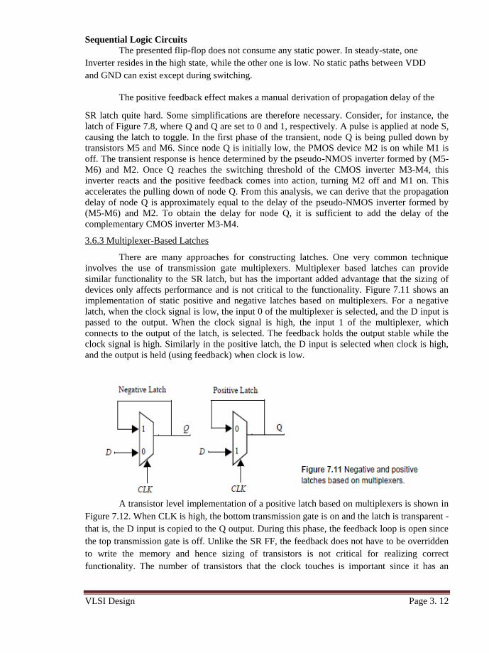
3.6.3 Multiplexer-Based Latches
There are many approaches for constructing latches. One very common technique
involves the use of transmission gate multiplexers. Multiplexer based latches can provide
similar functionality to the SR latch, but has the important added advantage that the sizing of
devices only affects performance and is not critical to the functionality. Figure 7.11 shows an
implementation of static positive and negative latches based on multiplexers. For a negative
latch, when the clock signal is low, the input 0 of the multiplexer is selected, and the D input is
passed to the output. When the clock signal is high, the input 1 of the multiplexer, which
connects to the output of the latch, is selected. The feedback holds the output stable while the
clock signal is high. Similarly in the positive latch, the D input is selected when clock is high,
and the output is held (using feedback) when clock is low.
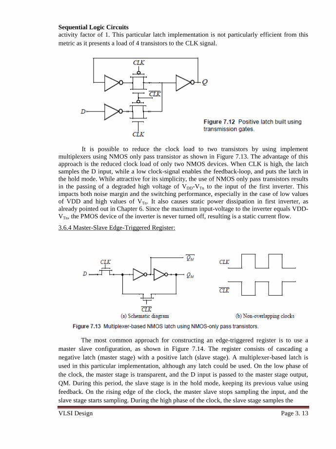
A transistor level implementation of a positive latch based on multiplexers is shown in
Figure 7.12. When CLK is high, the bottom transmission gate is on and the latch is transparent -
that is, the D input is copied to the Q output. During this phase, the feedback loop is open since
the top transmission gate is off. Unlike the SR FF, the feedback does not have to be overridden
to write the memory and hence sizing of transistors is not critical for realizing correct
functionality. The number of transistors that the clock touches is important since it has an
www.AllAbtEngg.com
AllAbtEngg Android Application for Anna University, Polytechnic & School
Sequential Logic Circuits
VLSI Design Page 3. 13
activity factor of 1. This particular latch implementation is not particularly efficient from this
metric as it presents a load of 4 transistors to the CLK signal.
It is possible to reduce the clock load to two transistors by using implement
multiplexers using NMOS only pass transistor as shown in Figure 7.13. The advantage of this
approach is the reduced clock load of only two NMOS devices. When CLK is high, the latch
samples the D input, while a low clock-signal enables the feedback-loop, and puts the latch in
the hold mode. While attractive for its simplicity, the use of NMOS only pass transistors results
in the passing of a degraded high voltage of VDD-VTn to the input of the first inverter. This
impacts both noise margin and the switching performance, especially in the case of low values
of VDD and high values of VTn. It also causes static power dissipation in first inverter, as
already pointed out in Chapter 6. Since the maximum input-voltage to the inverter equals VDD-
VTn, the PMOS device of the inverter is never turned off, resulting is a static current flow.
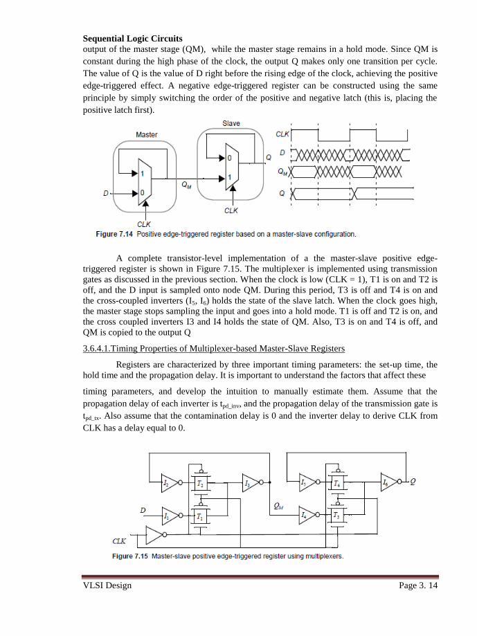
3.6.4 Master-Slave Edge-Triggered Register:
The most common approach for constructing an edge-triggered register is to use a
master slave configuration, as shown in Figure 7.14. The register consists of cascading a
negative latch (master stage) with a positive latch (slave stage). A multiplexer-based latch is
used in this particular implementation, although any latch could be used. On the low phase of
the clock, the master stage is transparent, and the D input is passed to the master stage output,
QM. During this period, the slave stage is in the hold mode, keeping its previous value using
feedback. On the rising edge of the clock, the master slave stops sampling the input, and the
slave stage starts sampling. During the high phase of the clock, the slave stage samples the
www.AllAbtEngg.com
AllAbtEngg Android Application for Anna University, Polytechnic & School
Sequential Logic Circuits
VLSI Design Page 3. 14
output of the master stage (QM), while the master stage remains in a hold mode. Since QM is
constant during the high phase of the clock, the output Q makes only one transition per cycle.
The value of Q is the value of D right before the rising edge of the clock, achieving the positive
edge-triggered effect. A negative edge-triggered register can be constructed using the same
principle by simply switching the order of the positive and negative latch (this is, placing the
positive latch first).
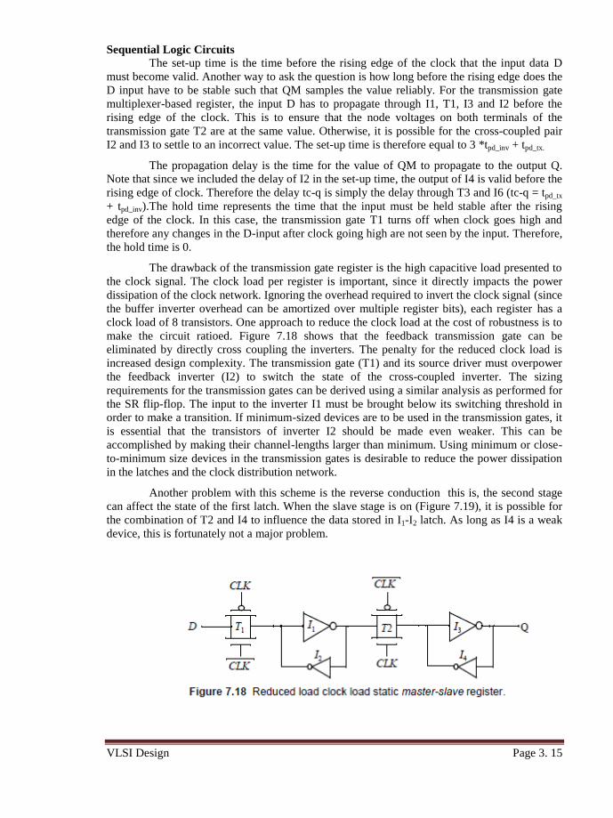
A complete transistor-level implementation of a the master-slave positive edge-
triggered register is shown in Figure 7.15. The multiplexer is implemented using transmission
gates as discussed in the previous section. When the clock is low (CLK = 1), T1 is on and T2 is
off, and the D input is sampled onto node QM. During this period, T3 is off and T4 is on and
the cross-coupled inverters (I5, I6) holds the state of the slave latch. When the clock goes high,
the master stage stops sampling the input and goes into a hold mode. T1 is off and T2 is on, and
the cross coupled inverters I3 and I4 holds the state of QM. Also, T3 is on and T4 is off, and
QM is copied to the output Q
3.6.4.1.Timing Properties of Multiplexer-based Master-Slave Registers
Registers are characterized by three important timing parameters: the set-up time, the
hold time and the propagation delay. It is important to understand the factors that affect these
timing parameters, and develop the intuition to manually estimate them. Assume that the
propagation delay of each inverter is tpd_inv, and the propagation delay of the transmission gate is
tpd_tx. Also assume that the contamination delay is 0 and the inverter delay to derive CLK from
CLK has a delay equal to 0.
www.AllAbtEngg.com
AllAbtEngg Android Application for Anna University, Polytechnic & School
Sequential Logic Circuits
VLSI Design Page 3. 15
The set-up time is the time before the rising edge of the clock that the input data D
must become valid. Another way to ask the question is how long before the rising edge does the
D input have to be stable such that QM samples the value reliably. For the transmission gate
multiplexer-based register, the input D has to propagate through I1, T1, I3 and I2 before the
rising edge of the clock. This is to ensure that the node voltages on both terminals of the
transmission gate T2 are at the same value. Otherwise, it is possible for the cross-coupled pair
I2 and I3 to settle to an incorrect value. The set-up time is therefore equal to 3 *tpd_inv + tpd_tx.
The propagation delay is the time for the value of QM to propagate to the output Q.
Note that since we included the delay of I2 in the set-up time, the output of I4 is valid before the
rising edge of clock. Therefore the delay tc-q is simply the delay through T3 and I6 (tc-q = tpd_tx
+ tpd_inv).The hold time represents the time that the input must be held stable after the rising
edge of the clock. In this case, the transmission gate T1 turns off when clock goes high and
therefore any changes in the D-input after clock going high are not seen by the input. Therefore,
the hold time is 0.
The drawback of the transmission gate register is the high capacitive load presented to
the clock signal. The clock load per register is important, since it directly impacts the power
dissipation of the clock network. Ignoring the overhead required to invert the clock signal (since
the buffer inverter overhead can be amortized over multiple register bits), each register has a
clock load of 8 transistors. One approach to reduce the clock load at the cost of robustness is to
make the circuit ratioed. Figure 7.18 shows that the feedback transmission gate can be
eliminated by directly cross coupling the inverters. The penalty for the reduced clock load is
increased design complexity. The transmission gate (T1) and its source driver must overpower
the feedback inverter (I2) to switch the state of the cross-coupled inverter. The sizing
requirements for the transmission gates can be derived using a similar analysis as performed for
the SR flip-flop. The input to the inverter I1 must be brought below its switching threshold in
order to make a transition. If minimum-sized devices are to be used in the transmission gates, it
is essential that the transistors of inverter I2 should be made even weaker. This can be
accomplished by making their channel-lengths larger than minimum. Using minimum or close-
to-minimum size devices in the transmission gates is desirable to reduce the power dissipation
in the latches and the clock distribution network.
Another problem with this scheme is the reverse conduction this is, the second stage
can affect the state of the first latch. When the slave stage is on (Figure 7.19), it is possible for
the combination of T2 and I4 to influence the data stored in I1-I2 latch. As long as I4 is a weak
device, this is fortunately not a major problem.
www.AllAbtEngg.com
AllAbtEngg Android Application for Anna University, Polytechnic & School
Sequential Logic Circuits
VLSI Design Page 3. 16
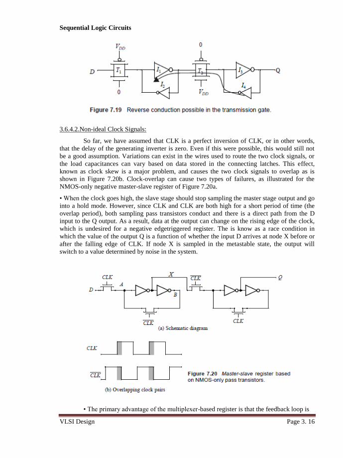
3.6.4.2.Non-ideal Clock Signals:
So far, we have assumed that CLK is a perfect inversion of CLK, or in other words,
that the delay of the generating inverter is zero. Even if this were possible, this would still not
be a good assumption. Variations can exist in the wires used to route the two clock signals, or
the load capacitances can vary based on data stored in the connecting latches. This effect,
known as clock skew is a major problem, and causes the two clock signals to overlap as is
shown in Figure 7.20b. Clock-overlap can cause two types of failures, as illustrated for the
NMOS-only negative master-slave register of Figure 7.20a.
• When the clock goes high, the slave stage should stop sampling the master stage output and go
into a hold mode. However, since CLK and CLK are both high for a short period of time (the
overlap period), both sampling pass transistors conduct and there is a direct path from the D
input to the Q output. As a result, data at the output can change on the rising edge of the clock,
which is undesired for a negative edgetriggered register. The is know as a race condition in
which the value of the output Q is a function of whether the input D arrives at node X before or
after the falling edge of CLK. If node X is sampled in the metastable state, the output will
switch to a value determined by noise in the system.
• The primary advantage of the multiplexer-based register is that the feedback loop is
www.AllAbtEngg.com
AllAbtEngg Android Application for Anna University, Polytechnic & School
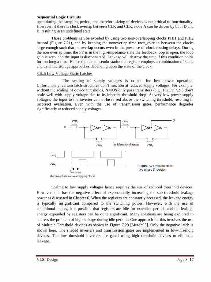
Sequential Logic Circuits
VLSI Design Page 3. 17
open during the sampling period, and therefore sizing of devices is not critical to functionality.
However, if there is clock overlap between CLK and CLK, node A can be driven by both D and
B, resulting in an undefined state.
Those problems can be avoided by using two non-overlapping clocks PHI1 and PHI2
instead (Figure 7.21), and by keeping the nonoverlap time tnon_overlap between the clocks
large enough such that no overlap occurs even in the presence of clock-routing delays. During
the non overlap time, the FF is in the high-impedance state the feedback loop is open, the loop
gain is zero, and the input is disconnected. Leakage will destroy the state if this condition holds
for too long a time. Hence the name pseudo-static: the register employs a combination of static
and dynamic storage approaches depending upon the state of the clock.
3.6..5 Low-Voltage Static Latches
The scaling of supply voltages is critical for low power operation.
Unfortunately, certain latch structures don’t function at reduced supply voltages. For example,
without the scaling of device thresholds, NMOS only pass transistors (e.g., Figure 7.21) don’t
scale well with supply voltage due to its inherent threshold drop. At very low power supply
voltages, the input to the inverter cannot be raised above the switching threshold, resulting in
incorrect evaluation. Even with the use of transmission gates, performance degrades
significantly at reduced supply voltages.
Scaling to low supply voltages hence requires the use of reduced threshold devices.
However, this has the negative effect of exponentially increasing the sub-threshold leakage
power as discussed in Chapter 6. When the registers are constantly accessed, the leakage energy
is typically insignificant compared to the switching power. However, with the use of
conditional clocks, it is possible that registers are idle for extended periods and the leakage
energy expended by registers can be quite significant. Many solutions are being explored to
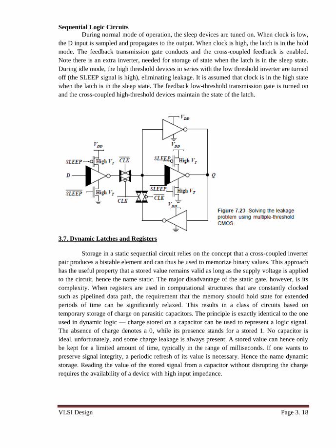
address the problem of high leakage during idle periods. One approach for this involves the use
of Multiple Threshold devices as shown in Figure 7.23 [Mutoh95]. Only the negative latch is
shown here. The shaded inverters and transmission gates are implemented in low-threshold
devices. The low threshold inverters are gated using high threshold devices to eliminate
leakage.
www.AllAbtEngg.com
AllAbtEngg Android Application for Anna University, Polytechnic & School
Sequential Logic Circuits
VLSI Design Page 3. 18
During normal mode of operation, the sleep devices are tuned on. When clock is low,
the D input is sampled and propagates to the output. When clock is high, the latch is in the hold
mode. The feedback transmission gate conducts and the cross-coupled feedback is enabled.
Note there is an extra inverter, needed for storage of state when the latch is in the sleep state.
During idle mode, the high threshold devices in series with the low threshold inverter are turned
off (the SLEEP signal is high), eliminating leakage. It is assumed that clock is in the high state
when the latch is in the sleep state. The feedback low-threshold transmission gate is turned on
and the cross-coupled high-threshold devices maintain the state of the latch.
3.7. Dynamic Latches and Registers
Storage in a static sequential circuit relies on the concept that a cross-coupled inverter
pair produces a bistable element and can thus be used to memorize binary values. This approach
has the useful property that a stored value remains valid as long as the supply voltage is applied
to the circuit, hence the name static. The major disadvantage of the static gate, however, is its
complexity. When registers are used in computational structures that are constantly clocked
such as pipelined data path, the requirement that the memory should hold state for extended
periods of time can be significantly relaxed. This results in a class of circuits based on
temporary storage of charge on parasitic capacitors. The principle is exactly identical to the one
used in dynamic logic — charge stored on a capacitor can be used to represent a logic signal.
The absence of charge denotes a 0, while its presence stands for a stored 1. No capacitor is
ideal, unfortunately, and some charge leakage is always present. A stored value can hence only
be kept for a limited amount of time, typically in the range of milliseconds. If one wants to
preserve signal integrity, a periodic refresh of its value is necessary. Hence the name dynamic
storage. Reading the value of the stored signal from a capacitor without disrupting the charge
requires the availability of a device with high input impedance.
www.AllAbtEngg.com
AllAbtEngg Android Application for Anna University, Polytechnic & School
Sequential Logic Circuits
VLSI Design Page 3. 19
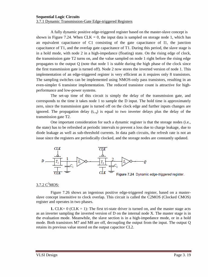
3.7.1 Dynamic Transmission-Gate Edge-triggered Registers
A fully dynamic positive edge-triggered register based on the master-slave concept is
shown in Figure 7.24. When CLK = 0, the input data is sampled on storage node 1, which has
an equivalent capacitance of C1 consisting of the gate capacitance of I1, the junction
capacitance of T1, and the overlap gate capacitance of T1. During this period, the slave stage is
in a hold mode, with node 2 in a high-impedance (floating) state. On the rising edge of clock,
the transmission gate T2 turns on, and the value sampled on node 1 right before the rising edge
propagates to the output Q (note that node 1 is stable during the high phase of the clock since
the first transmission gate is turned off). Node 2 now stores the inverted version of node 1. This
implementation of an edge-triggered register is very efficient as it requires only 8 transistors.
The sampling switches can be implemented using NMOS-only pass transistors, resulting in an
even-simpler 6 transistor implementation. The reduced transistor count is attractive for high-
performance and low-power systems.
The set-up time of this circuit is simply the delay of the transmission gate, and
corresponds to the time it takes node 1 to sample the D input. The hold time is approximately
zero, since the transmission gate is turned off on the clock edge and further inputs changes are
ignored. The propagation delay (tc-q) is equal to two inverter delays plus the delay of the
transmission gate T2.
One important consideration for such a dynamic register is that the storage nodes (i.e.,
the state) has to be refreshed at periodic intervals to prevent a loss due to charge leakage, due to
diode leakage as well as sub-threshold currents. In data path circuits, the refresh rate is not an
issue since the registers are periodically clocked, and the storage nodes are constantly updated.
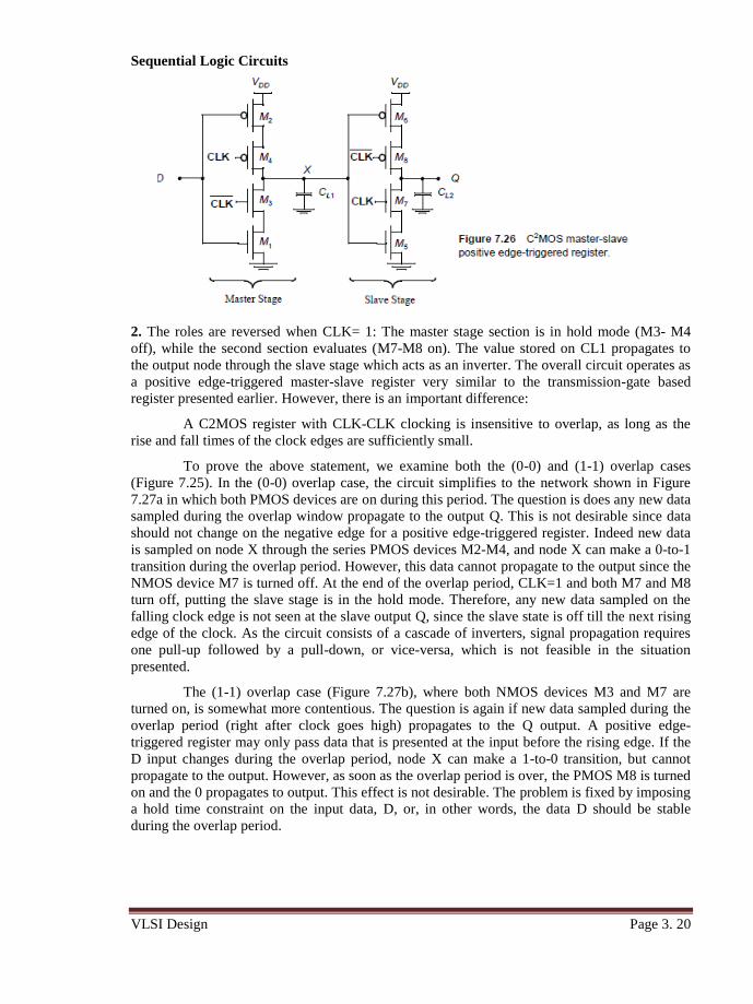
3.7.2 C2MOS:
Figure 7.26 shows an ingenious positive edge-triggered register, based on a master-
slave concept insensitive to clock overlap. This circuit is called the C2MOS (Clocked CMOS)
register and operates in two phases.
1. CLK= 0 (CLK = 1): The first tri-state driver is turned on, and the master stage acts
as an inverter sampling the inverted version of D on the internal node X. The master stage is in
the evaluation mode. Meanwhile, the slave section is in a high-impedance mode, or in a hold
mode. Both transistors M7 and M8 are off, decoupling the output from the input. The output Q
retains its previous value stored on the output capacitor CL2.
www.AllAbtEngg.com
AllAbtEngg Android Application for Anna University, Polytechnic & School
Sequential Logic Circuits
VLSI Design Page 3. 20
2. The roles are reversed when CLK= 1: The master stage section is in hold mode (M3- M4
off), while the second section evaluates (M7-M8 on). The value stored on CL1 propagates to
the output node through the slave stage which acts as an inverter. The overall circuit operates as
a positive edge-triggered master-slave register very similar to the transmission-gate based
register presented earlier. However, there is an important difference:
A C2MOS register with CLK-CLK clocking is insensitive to overlap, as long as the
rise and fall times of the clock edges are sufficiently small.
To prove the above statement, we examine both the (0-0) and (1-1) overlap cases
(Figure 7.25). In the (0-0) overlap case, the circuit simplifies to the network shown in Figure
7.27a in which both PMOS devices are on during this period. The question is does any new data
sampled during the overlap window propagate to the output Q. This is not desirable since data
should not change on the negative edge for a positive edge-triggered register. Indeed new data
is sampled on node X through the series PMOS devices M2-M4, and node X can make a 0-to-1
transition during the overlap period. However, this data cannot propagate to the output since the
NMOS device M7 is turned off. At the end of the overlap period, CLK=1 and both M7 and M8
turn off, putting the slave stage is in the hold mode. Therefore, any new data sampled on the
falling clock edge is not seen at the slave output Q, since the slave state is off till the next rising
edge of the clock. As the circuit consists of a cascade of inverters, signal propagation requires
one pull-up followed by a pull-down, or vice-versa, which is not feasible in the situation
presented.
The (1-1) overlap case (Figure 7.27b), where both NMOS devices M3 and M7 are
turned on, is somewhat more contentious. The question is again if new data sampled during the
overlap period (right after clock goes high) propagates to the Q output. A positive edge-
triggered register may only pass data that is presented at the input before the rising edge. If the
D input changes during the overlap period, node X can make a 1-to-0 transition, but cannot
propagate to the output. However, as soon as the overlap period is over, the PMOS M8 is turned
on and the 0 propagates to output. This effect is not desirable. The problem is fixed by imposing
a hold time constraint on the input data, D, or, in other words, the data D should be stable
during the overlap period.
www.AllAbtEngg.com
AllAbtEngg Android Application for Anna University, Polytechnic & School

Sequential Logic Circuits
VLSI Design Page 3. 21
In summary, it can be stated that the C2MOS latch is insensitive to clock overlaps
because those overlaps activate either the pull-up or the pull-down networks of the latches, but
never both of them simultaneously. If the rise and fall times of the clock are sufficiently slow,
however, there exists a time slot where both the NMOS and PMOS transistors are conducting.
This creates a path between input and output that can destroy the state of the circuit.
Simulations have shown that the circuit operates correctly as long as the clock rise time (or fall
time) is smaller than approximately five times the propagation delay of the register. This
criterion is not too stringent, and is easily met in practical designs.
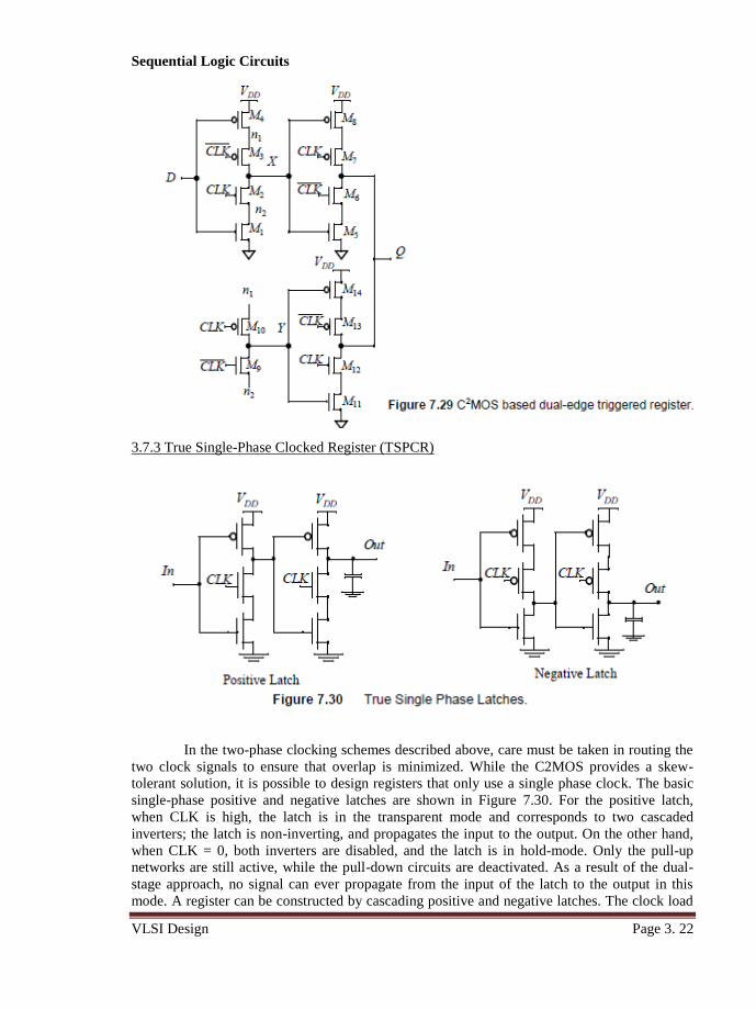
3.7.2 .1.Dual-edge Registers
So far, we have focused on edge-triggered registers that sample the input data on only
one of the clock edges (rising or falling). It is also possible to design sequential circuits that
sample the input on both edges. The advantage of this scheme is that a lower frequency clock
(half of the original rate) is distributed for the same functional throughput, resulting in power
savings in the clock distribution network. Figure 7.29 shows a modification of the C2MOS
register to enable sampling on both edges. It consists of two parallel master slave based edge-
triggered registers, whose outputs are multiplexed using the tri-state drivers.
When clock is high, the positive latch composed of transistors M1-M4 is sampling the
inverted D input on node X. Node Y is held stable, since devices M9 and M10 are turned off.
On the falling edge of the clock, the top slave latch M5-M8 turns on, and drives the inverted
value of X to the Q output. During the low phase, the bottom master latch (M1, M4, M9, M10)
is turned on, sampling the inverted D input on node Y. Note that the devices M1 and M4 are
reused, reducing the load on the D input. On the rising edge, the bottom slave latch conducts,
and drives the inverted version of Y on node Q. Data hence changes on both edges.
www.AllAbtEngg.com
AllAbtEngg Android Application for Anna University, Polytechnic & School
Sequential Logic Circuits
VLSI Design Page 3. 22
3.7.3 True Single-Phase Clocked Register (TSPCR)
In the two-phase clocking schemes described above, care must be taken in routing the
two clock signals to ensure that overlap is minimized. While the C2MOS provides a skew-
tolerant solution, it is possible to design registers that only use a single phase clock. The basic
single-phase positive and negative latches are shown in Figure 7.30. For the positive latch,
when CLK is high, the latch is in the transparent mode and corresponds to two cascaded
inverters; the latch is non-inverting, and propagates the input to the output. On the other hand,
when CLK = 0, both inverters are disabled, and the latch is in hold-mode. Only the pull-up
networks are still active, while the pull-down circuits are deactivated. As a result of the dual-
stage approach, no signal can ever propagate from the input of the latch to the output in this
mode. A register can be constructed by cascading positive and negative latches. The clock load
www.AllAbtEngg.com
AllAbtEngg Android Application for Anna University, Polytechnic & School
Sequential Logic Circuits
VLSI Design Page 3. 23
is similar to a conventional transmission gate register, or C2MOS register. The main advantage
is the use of a single clock phase.
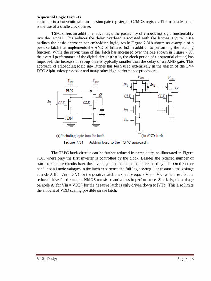
TSPC offers an additional advantage: the possibility of embedding logic functionality
into the latches. This reduces the delay overhead associated with the latches. Figure 7.31a
outlines the basic approach for embedding logic, while Figure 7.31b shows an example of a
positive latch that implements the AND of In1 and In2 in addition to performing the latching
function. While the set-up time of this latch has increased over the one shown in Figure 7.30,
the overall performance of the digital circuit (that is, the clock period of a sequential circuit) has
improved: the increase in set-up time is typically smaller than the delay of an AND gate. This
approach of embedding logic into latches has been used extensively in the design of the EV4
DEC Alpha microprocessor and many other high performance processors.
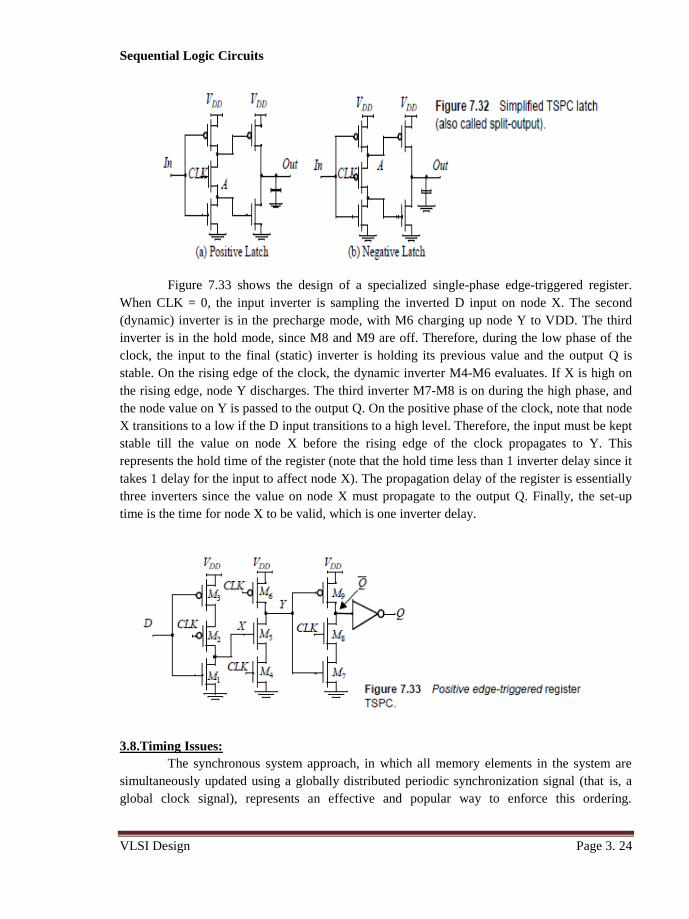
The TSPC latch circuits can be further reduced in complexity, as illustrated in Figure
7.32, where only the first inverter is controlled by the clock. Besides the reduced number of
transistors, these circuits have the advantage that the clock load is reduced by half. On the other
hand, not all node voltages in the latch experience the full logic swing. For instance, the voltage
at node A (for Vin = 0 V) for the positive latch maximally equals VDD – VTn, which results in a
reduced drive for the output NMOS transistor and a loss in performance. Similarly, the voltage
on node A (for Vin = VDD) for the negative latch is only driven down to |VTp|. This also limits
the amount of VDD scaling possible on the latch.
www.AllAbtEngg.com
AllAbtEngg Android Application for Anna University, Polytechnic & School
Sequential Logic Circuits
VLSI Design Page 3. 24
Figure 7.33 shows the design of a specialized single-phase edge-triggered register.
When CLK = 0, the input inverter is sampling the inverted D input on node X. The second
(dynamic) inverter is in the precharge mode, with M6 charging up node Y to VDD. The third
inverter is in the hold mode, since M8 and M9 are off. Therefore, during the low phase of the
clock, the input to the final (static) inverter is holding its previous value and the output Q is
stable. On the rising edge of the clock, the dynamic inverter M4-M6 evaluates. If X is high on
the rising edge, node Y discharges. The third inverter M7-M8 is on during the high phase, and
the node value on Y is passed to the output Q. On the positive phase of the clock, note that node
X transitions to a low if the D input transitions to a high level. Therefore, the input must be kept
stable till the value on node X before the rising edge of the clock propagates to Y. This
represents the hold time of the register (note that the hold time less than 1 inverter delay since it
takes 1 delay for the input to affect node X). The propagation delay of the register is essentially
three inverters since the value on node X must propagate to the output Q. Finally, the set-up
time is the time for node X to be valid, which is one inverter delay.
3.8.Timing Issues:
The synchronous system approach, in which all memory elements in the system are
simultaneously updated using a globally distributed periodic synchronization signal (that is, a
global clock signal), represents an effective and popular way to enforce this ordering.
www.AllAbtEngg.com
AllAbtEngg Android Application for Anna University, Polytechnic & School

Sequential Logic Circuits
VLSI Design Page 3. 25
Functionality is ensured by imposing some strict constraints on the generation of the clock
signals and their distribution to the memory elements distributed over the chip; non-compliance
often leads to malfunction.
This We analyze the impact of spatial variations of the clock signal, called clock skew,
and temporal variations of the clock signal, called clock jitter, and introduce techniques to cope
with it. These variations fundamentally limit the performance that can be achieved using a
conventional design methodology.
Asynchronous design, which avoids the problem of clock uncertainty all together by
eliminating the need for globally-distributed clocks. The important issue of synchronization,
which is required when interfacing different clock domains or when sampling an asynchronous
signal, also deserves some in-depth treatment.
3.8.1 Classification of Digital Systems
In digital systems, signals can be classified depending on how they are related to a
local clock. Signals that transition only at predetermined periods in time can be classified as
synchronous, mesochronous, or plesiochronous with respect to a system clock. A signal that can
transition at arbitrary times is considered asynchronous.
3.8.1.1 Synchronous Interconnect
A synchronous signal is one that has the exact same frequency, and a known fixed
phase offset with respect to the local clock. In such a timing methodology, the signal is
―synchronized‖ with the clock, and the data can be sampled directly without any uncertainty. In
digital logic design, synchronous systems are the most straight forward type of interconnect,
where the flow of data in a circuit proceeds in lockstep with the system clock as shown below.
Here, the input data signal is sampled with register R1 to give signal Cin, which is
synchronous with the system clock and then passed along to the combinational logic block.
After a suitable setting period, the output Cout becomes valid and can be sampled by R2 which
synchronizes the output with the clock. In a sense, the ―certainty period‖ of signal Cout, or the
period where data is valid is synchronized with the system clock, which allows register R2 to
sample the data with complete confidence. The length of the ―uncertainty period,‖ or the period
where data is not valid, places an upper bound on how fast a synchronous interconnect system
can be clocked.
3.8.1.2 Mesochronous interconnect
A mesochronous signal is one that has the same frequency but an unknown phase
offset with respect to the local clock (―meso‖ from Greek is middle). For example, if data is
being passed between two different clock domains, then the data signal transmitted from the
first module can have an unknown phase relationship to the clock of the receiving module. In
such a system, it is not possible to directly sample the output at the receiving module because of
the uncertainty in the phase offset. A (mesochronous) synchronizer can be used to synchronize
www.AllAbtEngg.com
AllAbtEngg Android Application for Anna University, Polytechnic & School
Sequential Logic Circuits
VLSI Design Page 3. 26
the data signal with the receiving clock as shown below. The synchronizer serves to adjust the
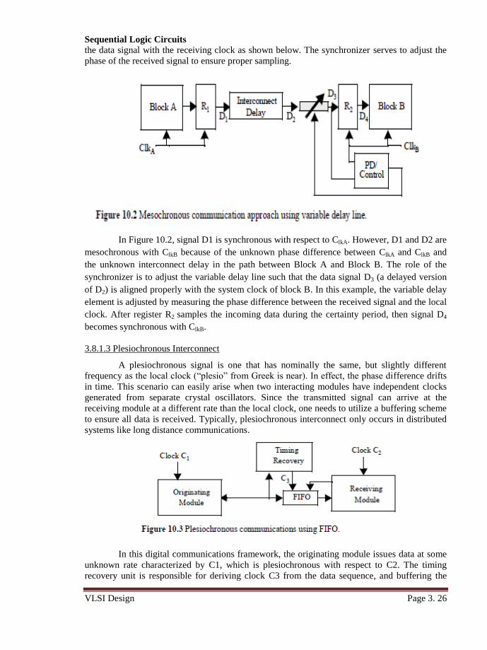
phase of the received signal to ensure proper sampling.
In Figure 10.2, signal D1 is synchronous with respect to ClkA. However, D1 and D2 are
mesochronous with ClkB because of the unknown phase difference between ClkA and ClkB and
the unknown interconnect delay in the path between Block A and Block B. The role of the
synchronizer is to adjust the variable delay line such that the data signal D3 (a delayed version
of D2) is aligned properly with the system clock of block B. In this example, the variable delay
element is adjusted by measuring the phase difference between the received signal and the local
clock. After register R2 samples the incoming data during the certainty period, then signal D4
becomes synchronous with ClkB.
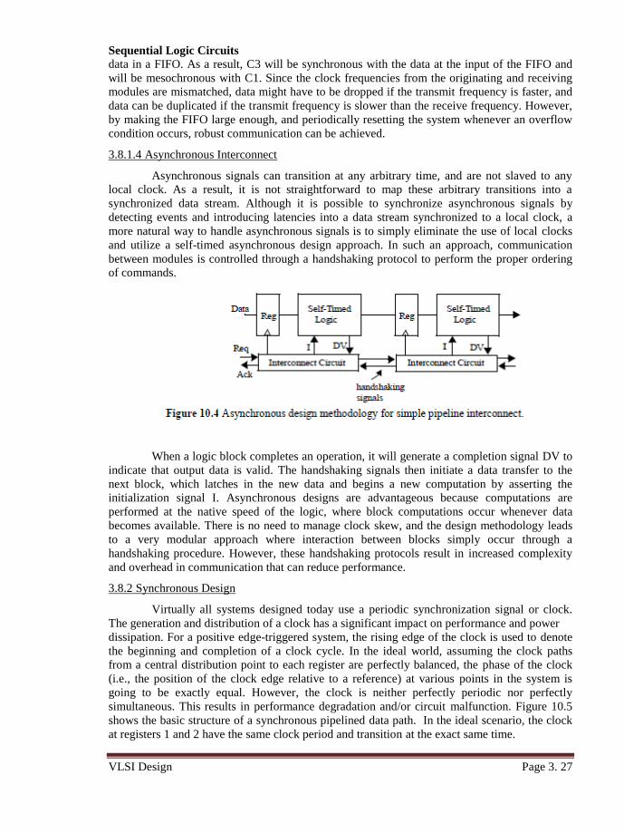
3.8.1.3 Plesiochronous Interconnect
A plesiochronous signal is one that has nominally the same, but slightly different
frequency as the local clock (―plesio‖ from Greek is near). In effect, the phase difference drifts
in time. This scenario can easily arise when two interacting modules have independent clocks
generated from separate crystal oscillators. Since the transmitted signal can arrive at the
receiving module at a different rate than the local clock, one needs to utilize a buffering scheme
to ensure all data is received. Typically, plesiochronous interconnect only occurs in distributed
systems like long distance communications.
In this digital communications framework, the originating module issues data at some
unknown rate characterized by C1, which is plesiochronous with respect to C2. The timing
recovery unit is responsible for deriving clock C3 from the data sequence, and buffering the
www.AllAbtEngg.com
AllAbtEngg Android Application for Anna University, Polytechnic & School
Sequential Logic Circuits
VLSI Design Page 3. 27
data in a FIFO. As a result, C3 will be synchronous with the data at the input of the FIFO and
will be mesochronous with C1. Since the clock frequencies from the originating and receiving
modules are mismatched, data might have to be dropped if the transmit frequency is faster, and
data can be duplicated if the transmit frequency is slower than the receive frequency. However,
by making the FIFO large enough, and periodically resetting the system whenever an overflow
condition occurs, robust communication can be achieved.
3.8.1.4 Asynchronous Interconnect
Asynchronous signals can transition at any arbitrary time, and are not slaved to any
local clock. As a result, it is not straightforward to map these arbitrary transitions into a
synchronized data stream. Although it is possible to synchronize asynchronous signals by
detecting events and introducing latencies into a data stream synchronized to a local clock, a
more natural way to handle asynchronous signals is to simply eliminate the use of local clocks
and utilize a self-timed asynchronous design approach. In such an approach, communication
between modules is controlled through a handshaking protocol to perform the proper ordering
of commands.
When a logic block completes an operation, it will generate a completion signal DV to
indicate that output data is valid. The handshaking signals then initiate a data transfer to the
next block, which latches in the new data and begins a new computation by asserting the
initialization signal I. Asynchronous designs are advantageous because computations are
performed at the native speed of the logic, where block computations occur whenever data
becomes available. There is no need to manage clock skew, and the design methodology leads
to a very modular approach where interaction between blocks simply occur through a
handshaking procedure. However, these handshaking protocols result in increased complexity
and overhead in communication that can reduce performance.
3.8.2 Synchronous Design
Virtually all systems designed today use a periodic synchronization signal or clock.
The generation and distribution of a clock has a significant impact on performance and power
dissipation. For a positive edge-triggered system, the rising edge of the clock is used to denote
the beginning and completion of a clock cycle. In the ideal world, assuming the clock paths
from a central distribution point to each register are perfectly balanced, the phase of the clock
(i.e., the position of the clock edge relative to a reference) at various points in the system is
going to be exactly equal. However, the clock is neither perfectly periodic nor perfectly
simultaneous. This results in performance degradation and/or circuit malfunction. Figure 10.5
shows the basic structure of a synchronous pipelined data path. In the ideal scenario, the clock
at registers 1 and 2 have the same clock period and transition at the exact same time.
www.AllAbtEngg.com
AllAbtEngg Android Application for Anna University, Polytechnic & School

Sequential Logic Circuits
VLSI Design Page 3. 28
At the same time, the hold time of the destination register must be shorter than the minimum
propagation delay through the logic network, the clock signal can have spatial and temporal
variations.
Clock Skew
The spatial variation in arrival time of a clock transition on an integrated circuit is
commonly referred to as clock skew. The timing diagram for the case with positive skew is
shown in Figure 10.6. As the figure illustrates, the rising clock edge is delayed by a positive at
the second register.
• δ> 0—This corresponds to a clock routed in the same direction as the flow of the data through
the pipeline (Figure 10.8a). positive skew increases the throughput of the circuit, because the
clock period can be shortened by δ. The extent of this improvement is limited as large values of
δ .
• δ < 0—When the clock is routed in the opposite direction of the data, the skew is negative The
circuit operates correctly independent of the skew. The skew reduces the time available for
actual computation so that the clock period has to be increased by | δ|. The skew can assume
both positive and negative values depending on the direction of the data transfer. Under these
circumstances, the designer has to account for the worst-case skew condition. In general,
www.AllAbtEngg.com
AllAbtEngg Android Application for Anna University, Polytechnic & School
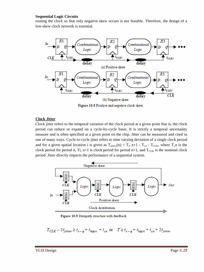
Sequential Logic Circuits
VLSI Design Page 3. 29
routing the clock so that only negative skew occurs is not feasible. Therefore, the design of a
low-skew clock network is essential.
Clock Jitter
Clock jitter refers to the temporal variation of the clock period at a given point that is, the clock
period can reduce or expand on a cycle-by-cycle basis. It is strictly a temporal uncertainty
measure and is often specified at a given point on the chip. Jitter can be measured and cited in
one of many ways. Cycle-to-cycle jitter refers to time varying deviation of a single clock period
and for a given spatial location i is given as Tjitter,i(n) = Ti, n+1 - Ti,n - TCLK, where Ti,n is the
clock period for period n, Ti, n+1 is clock period for period n+1, and TCLK is the nominal clock
period. Jitter directly impacts the performance of a sequential system.
www.AllAbtEngg.com
AllAbtEngg Android Application for Anna University, Polytechnic & School

Sequential Logic Circuits
VLSI Design Page 3. 30
The above equation illustrates that jitter directly reduces the performance of a
sequential circuit. Care must be taken to reduce jitter in the clock network to maximize
performance.
The combined Impact of Skew and Jitter on Performance:
The given equation illustrates, while positive skew can provide potential
performance advantage, jitter has a negative impact on the minimum clock period. To formulate
the minimum delay constraint, consider the case when the leading edge of the CLK1 cycle
arrives early (edge 1) and the leading edge the current cycle of CLK2 arrives late (edge 6). The
separation between edge 1 and 6 should be smaller than the minimum delay through the
network. This results in The above relation indicates that the acceptable skew is reduced by the
jitter of the two signals.
www.AllAbtEngg.com
AllAbtEngg Android Application for Anna University, Polytechnic & School
Sequential Logic Circuits
VLSI Design Page 3. 31
3.8.2.2 Sources of Skew and Jitter
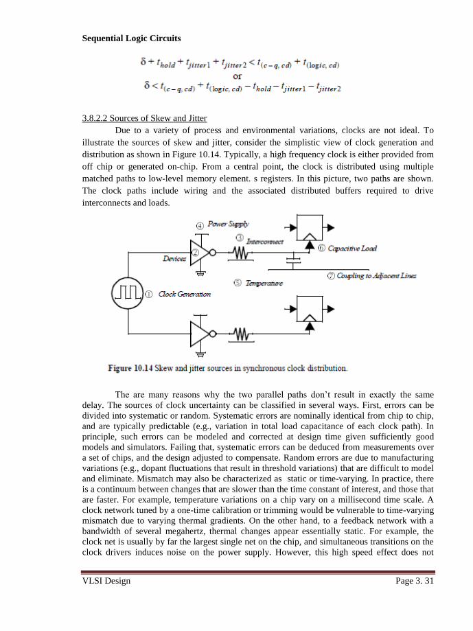
Due to a variety of process and environmental variations, clocks are not ideal. To
illustrate the sources of skew and jitter, consider the simplistic view of clock generation and
distribution as shown in Figure 10.14. Typically, a high frequency clock is either provided from
off chip or generated on-chip. From a central point, the clock is distributed using multiple
matched paths to low-level memory element. s registers. In this picture, two paths are shown.
The clock paths include wiring and the associated distributed buffers required to drive
interconnects and loads.
The are many reasons why the two parallel paths don’t result in exactly the same
delay. The sources of clock uncertainty can be classified in several ways. First, errors can be
divided into systematic or random. Systematic errors are nominally identical from chip to chip,
and are typically predictable (e.g., variation in total load capacitance of each clock path). In
principle, such errors can be modeled and corrected at design time given sufficiently good
models and simulators. Failing that, systematic errors can be deduced from measurements over
a set of chips, and the design adjusted to compensate. Random errors are due to manufacturing
variations (e.g., dopant fluctuations that result in threshold variations) that are difficult to model
and eliminate. Mismatch may also be characterized as static or time-varying. In practice, there
is a continuum between changes that are slower than the time constant of interest, and those that
are faster. For example, temperature variations on a chip vary on a millisecond time scale. A
clock network tuned by a one-time calibration or trimming would be vulnerable to time-varying
mismatch due to varying thermal gradients. On the other hand, to a feedback network with a
bandwidth of several megahertz, thermal changes appear essentially static. For example, the
clock net is usually by far the largest single net on the chip, and simultaneous transitions on the
clock drivers induces noise on the power supply. However, this high speed effect does not
www.AllAbtEngg.com
AllAbtEngg Android Application for Anna University, Polytechnic & School
Sequential Logic Circuits
VLSI Design Page 3. 32
contribute to time-varying mismatch because it is the same on every clock cycle, affecting each
rising clock edge the same way.
3.8.2.3 Clock-Distribution Techniques
It is clear from the previous discussion that clock skew and jitter are major issues in
digital circuits, and can fundamentally limit the performance of a digital system. It is necessary
to design a clock network that minimizes skew and jitter. Another important consideration in
clock distribution is the power dissipation. In most high-speed digital processors, a majority of
the power is dissipated in the clock network. To reduce power dissipation, clock networks must
support clock conditioning — this is, the ability to shut down parts of the clock network.
Unfortunately, clock gating results in additional clock uncertainty. In this section, an overview
of basic constructs in high-performance clock distribution techniques is presented along with a
case study of clock distribution in the Alpha microprocessor. There are many degrees of
freedom in the design of a clock network including the type of material used for wires, the basic
topology and hierarchy, the sizing of wires and buffers, the rise and fall times, and the
partitioning of load capacitances.
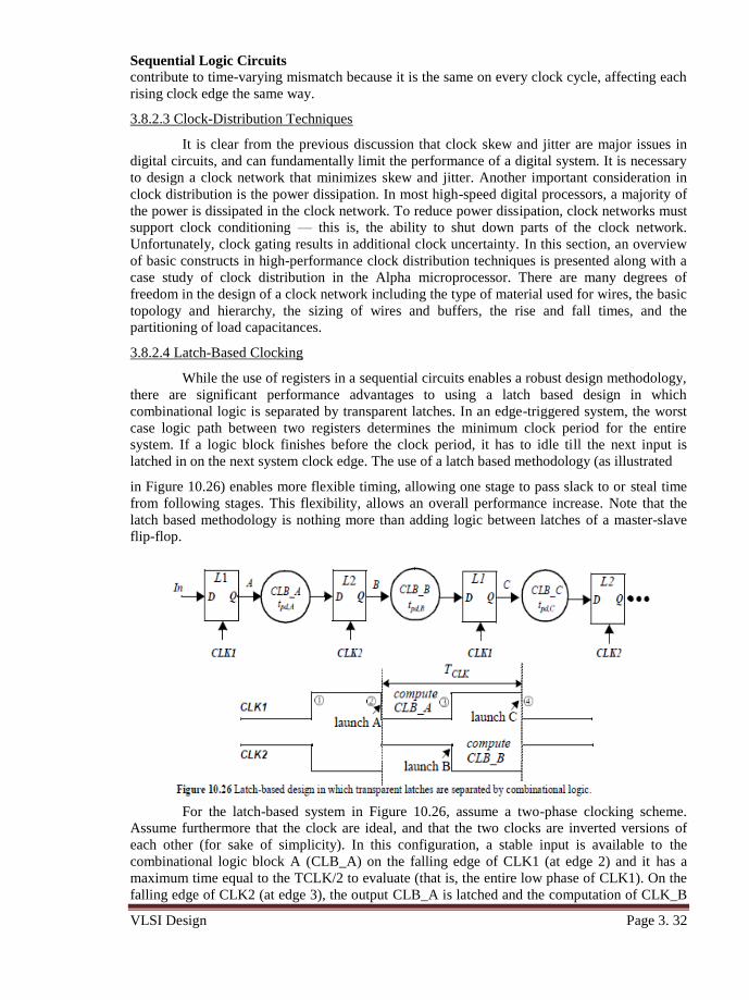
3.8.2.4 Latch-Based Clocking
While the use of registers in a sequential circuits enables a robust design methodology,
there are significant performance advantages to using a latch based design in which
combinational logic is separated by transparent latches. In an edge-triggered system, the worst
case logic path between two registers determines the minimum clock period for the entire
system. If a logic block finishes before the clock period, it has to idle till the next input is
latched in on the next system clock edge. The use of a latch based methodology (as illustrated
in Figure 10.26) enables more flexible timing, allowing one stage to pass slack to or steal time
from following stages. This flexibility, allows an overall performance increase. Note that the
latch based methodology is nothing more than adding logic between latches of a master-slave
flip-flop.
For the latch-based system in Figure 10.26, assume a two-phase clocking scheme.
Assume furthermore that the clock are ideal, and that the two clocks are inverted versions of
each other (for sake of simplicity). In this configuration, a stable input is available to the
combinational logic block A (CLB_A) on the falling edge of CLK1 (at edge 2) and it has a
maximum time equal to the TCLK/2 to evaluate (that is, the entire low phase of CLK1). On the
falling edge of CLK2 (at edge 3), the output CLB_A is latched and the computation of CLK_B
www.AllAbtEngg.com
AllAbtEngg Android Application for Anna University, Polytechnic & School
Sequential Logic Circuits
VLSI Design Page 3. 33
is launched. CLB_B computes on the low phase of CLK2 and the output is available on the
falling edge of CLK1 (at edge 4). This timing appears equivalent to having an edge-triggered
system where CLB_A and CLB_B are cascaded and between two edge-triggered registers
(Figure 10.27). In both cases, it appears that the time available to perform the combination of
CLB_A and CLB_B is TCLK.
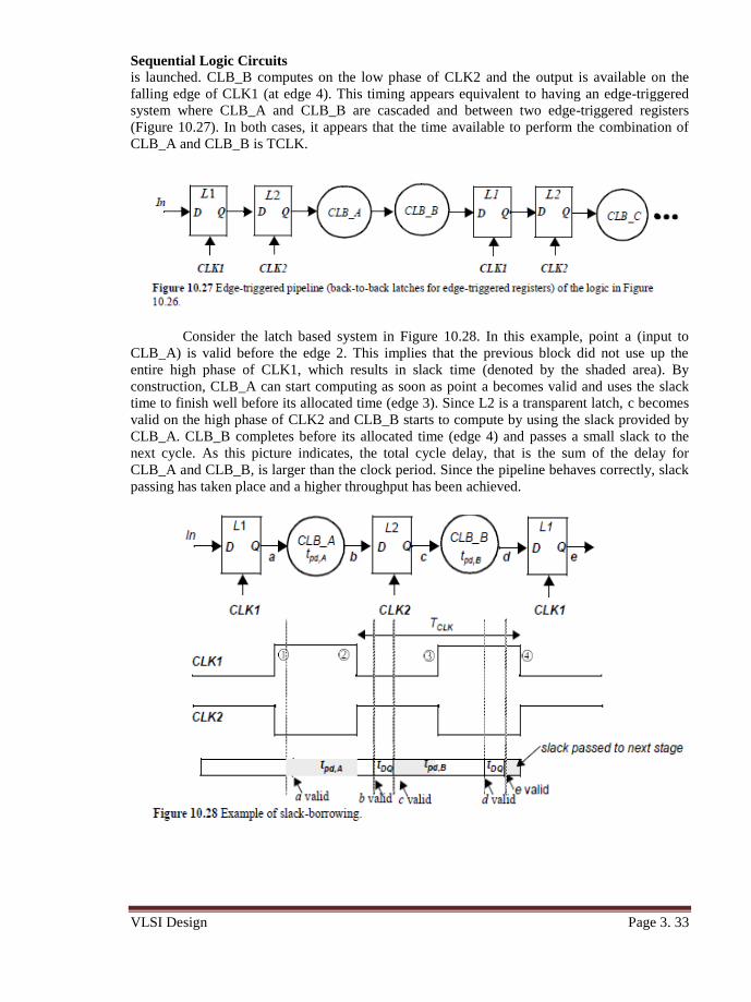
Consider the latch based system in Figure 10.28. In this example, point a (input to
CLB_A) is valid before the edge 2. This implies that the previous block did not use up the
entire high phase of CLK1, which results in slack time (denoted by the shaded area). By
construction, CLB_A can start computing as soon as point a becomes valid and uses the slack
time to finish well before its allocated time (edge 3). Since L2 is a transparent latch, c becomes
valid on the high phase of CLK2 and CLB_B starts to compute by using the slack provided by
CLB_A. CLB_B completes before its allocated time (edge 4) and passes a small slack to the
next cycle. As this picture indicates, the total cycle delay, that is the sum of the delay for
CLB_A and CLB_B, is larger than the clock period. Since the pipeline behaves correctly, slack
passing has taken place and a higher throughput has been achieved.
www.AllAbtEngg.com
AllAbtEngg Android Application for Anna University, Polytechnic & School

Sequential Logic Circuits
VLSI Design Page 3. 34
An important question related to slack passing relates to the maximum possible slack
that can be passed across cycle boundaries. In Figure 10.28, it is easy that see that the earliest
time that CLB_A can start computing is 1. This happens if the previous logic block did not use
any of its allocated time (CLK1 high phase) or if it finished by using slack from previous
stages. Therefore, the maximum time that can be borrowed from the previous stage is 1/2 cycle
or TCLK/2. Similarly, CLB_B must finish its operation by edge 4. This implies that the
maximum logic cycle delay is equal to 1.5 * TCLK. However, note that for an n-stage pipeline,
, the overall logic delay cannot exceed the time available of n * TCLK.
3.8. 3 Self-Timed Circuit Design
3.8. 3.1 Self-Timed Logic - An Asynchronous Technique
The synchronous design approach advocated in the previous sections assumes that all
circuit events are orchestrated by a central clock. Those clocks have a dual function.
• They insure that the physical timing constraints are met. The next clock cycle can only start
when all logic transitions have settled and the system has come to a steady state. This ensures
that only legal logical values are applied in the next round of computation. In short, clocks
account for the worst case delays of logic gates, sequential logic elements and the wiring.
• Clock events serve as a logical ordering mechanism for the global system events. A clock
provides a time base that determines what will happen and when. On every clock transition, a
number of operations are initiated that change the state of the sequential network. Consider the
pipelined datapath of Figure 10.31. In this circuit, the data transitions through logic stages under
the command of the clock. The important point to note under this methodology is that the clock
period is chosen to be larger than the worst-case delay of each pipeline stage, or T > max (tpd1,
tpd2, tpd3) + tpd,reg. This will ensure satisfying the physical constraint. At each clock
transition, a new set of inputs is sampled and computation is started anew. The throughput of
the system—which is equivalent to the number of data samples processed per second—is
equivalent to the clock rate. When to sample a new input or when an output is available
depends upon the logical ordering of the system events and is clearly orchestrated by the clock
in this example.
The synchronous design methodology has some clear advantages. It presents a
structured, deterministic approach to the problem of choreographing the myriad of events that
take place in digital designs. The approach taken is to equalize the delays of all operations by
making them as bad as the worst of the set. The approach is robust and easy to adhere to, which
explains its enormous popularity; however it does have some pitfalls. • It assumes that all clock
events or timing references happen simultaneously over the complete circuit. This is not the
case in reality, because of effects such as clock skew and jitter.
www.AllAbtEngg.com
AllAbtEngg Android Application for Anna University, Polytechnic & School
Sequential Logic Circuits
VLSI Design Page 3. 35
Figure 10.32 uses a pipelined datapath to illustrate how this can be accomplished. This
approach assumes that each combinational function has a means of indicating that it has
completed a computation for a particular piece of data. The computation of a logic block is
initiated by asserting a Start signal. The combinational logic block computes on the input data
and in a data-dependent fashion (taking the physical constraints into account) generates a Done
flag once the computation is finished. Additionally, the operators must signal each other that
they are either ready to receive a next input word or that they have a legal data word at their
outputs that is ready for consumption. This signaling ensures the logical ordering of the events
and can be achieved with the aid of an extra Ack(nowledge) and Req(uest) signal.
3.8. 3.2 Completion-Signal Generation
A necessary component of self-timed logic is the circuitry to indicate when a particular
piece of circuitry has completed its operation for the current piece of data. There are two
common and reliable ways to generate the completion signal.
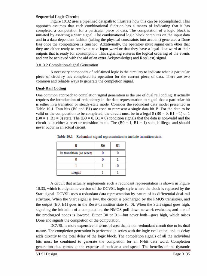
Dual-Rail Coding
One common approach to completion signal generation is the use of dual rail coding. It actually
requires the introduction of redundancy in the data representation to signal that a particular bit
is either in a transition or steady-state mode. Consider the redundant data model presented in
Table 10.1. Two bits (B0 and B1) are used to represent a single data bit B. For the data to be
valid or the computation to be completed, the circuit must be in a legal 0 (B0 = 0, B1 = 1) or 1
(B0 = 1, B1 = 0) state. The (B0 = 0, B1 = 0) condition signals that the data is non-valid and the
circuit is in either a reset or transition mode. The (B0 = 1, B1 = 1) state is illegal and should
never occur in an actual circuit.
A circuit that actually implements such a redundant representation is shown in Figure
10.33, which is a dynamic version of the DCVSL logic style where the clock is replaced by the
Start signal. DCVSL uses a redundant data representation by nature of its differential dual-rail
structure. When the Start signal is low, the circuit is precharged by the PMOS transistors, and
the output (B0, B1) goes in the Reset-Transition state (0, 0). When the Start signal goes high,
signaling the initiation of a computation, the NMOS pull-down network evaluates, and one of
the precharged nodes is lowered. Either B0 or B1—but never both—goes high, which raises
Done and signals the completion of the computation.
DCVSL is more expensive in terms of area than a non-redundant circuit due to its dual
nature. The completion generation is performed in series with the logic evaluation, and its delay
adds directly to the total delay of the logic block. The completion signals of all the individual
bits must be combined to generate the completion for an N-bit data word. Completion
generation thus comes at the expense of both area and speed. The benefits of the dynamic
www.AllAbtEngg.com
AllAbtEngg Android Application for Anna University, Polytechnic & School

Sequential Logic Circuits
VLSI Design Page 3. 36
timing generation often justify this overhead. Redundant signal presentations other than the one
presented in Table 10.1 can also be envisioned. One essential element is the presence of a
transition state denoting that the circuit is in evaluation mode and the output data is not valid.
3.8. 3.3.Self-Timed Signaling
Besides the generation of the completion signals, a self-timed approach also requires a
handshaking protocol to logically order the circuit events avoiding races and hazards. The
functionality of the signaling (or handshaking) logic is illustrated by the example of Figure
10.37, which shows a sender module transmitting data to a receiver.
The sender places the data value on the data bus 1 and produces an event on the Req
control signal by changing the polarity of the signal 2. In some cases the request event is a
rising transition; at other times it is a falling one—the protocol described here does not
distinguish between them. Upon receiving the request, the receiver accepts the data when
possible and produces an event on the Ack signal to indicate that the data has been accepted 3.
If the receiver is busy or its input buffer is full, no Ack event is generated, and the transmitter is
stalled until the receiver becomes available by, for instance, freeing space in the input buffer.
Once the Ack event is produced, the transmitter goes ahead and produces the next data word 1.
The four events, data change, request, data acceptance, and acknowledge, proceed in a cyclic
www.AllAbtEngg.com
AllAbtEngg Android Application for Anna University, Polytechnic & School

Sequential Logic Circuits
VLSI Design Page 3. 37
order. Successive cycles may take different amounts of time depending upon the time it takes to
produce or consume the data.
This protocol is called two-phase, since only two phases of operation can be
distinguished for each data transmission—the active cycle of the sender and the active cycle of
the receiver. Both phases are terminated by certain events. The Req event terminates the active
cycle of the sender, while the receiver’s cycle is completed by the Ack event. The sender is free
to change the data during its active cycle. Once the Req event is generated, it has to keep the
data constant as long as the receiver is active. The receiver can only accept
data during its active cycle.
The correct operation of the sender-receiver system requires a strict ordering of the
signaling events, as indicated by the arrows in Figure 10.37. Imposing this order is the task of
the handshaking logic which, in a sense, performs logic manipulations on events. An essential
component of virtually any handshaking module is the Muller C-element. This gate, whose
schematic symbol and truth table are given in Figure 10.38, performs an AND-operation on
events. The output of the C-element is a copy of its inputs when both inputs are identical. When
the inputs differ, the output retains its previous value. Phrased in a different way—events must
occur at both inputs of a Muller C-element for its output to change state and to create an output
event. As long as this does not happen, the output remains unchanged and no output event is
generated. The implementation of a C-element is centered around a flip-flop, which should be
of no surprise, given the similarities in their truth tables.
Figure 10.40 shows how to use this component to enforce the two-phase handshaking
protocol for the example of the sender-receiver. Assume that Req, Ack, and Data Ready are
initially 0. When the sender wants to transmit the next word, the Data Ready signal is set to 1,
which triggers the C-element because both its inputs are at 1. Req goes high—this is commonly
www.AllAbtEngg.com
AllAbtEngg Android Application for Anna University, Polytechnic & School
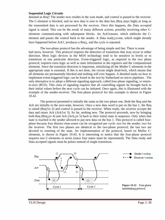
Sequential Logic Circuits
VLSI Design Page 3. 38
denoted as Req↑ The sender now resides in the wait mode, and control is passed to the receiver.
The C-element is blocked, and no new data is sent to the data bus (Req stays high) as long as
the transmitted data is not processed by the receiver. Once this happens, the Data accepted
signal is raised. This can be the result of many different actions, possibly involving other C-
elements communicating with subsequent blocks. An Ack↑ensues, which unblocks the C-
element and passes the control back to the sender. A Data ready↓event, which might already
have happened before Ack↑, produces a Req↓, and the cycle is repeated.
The two-phase protocol has the advantage of being simple and fast. There is some
bad news, however. This protocol requires the detection of transitions that may occur in either
direction. Most logic devices in the MOS technology tend to be sensitive to levels or to
transitions in one particular direction. Event-triggered logic, as required in the two phase
protocol, requires extra logic as well as state information in the registers and the computational
elements. Since the transition direction is important, initializing all the Muller C-elements in the
appropriate state is essential. If this is not done, the circuit might dead-lock, which means that
all elements are permanently blocked and nothing will ever happen. A detailed study on how to
implement event-triggered logic can be found in the text by Sutherland on micro pipelines . The
only alternative is to adopt a different signaling approach, called four-phase signaling, or return-
to-zero (RTZ). This class of signaling requires that all controlling signals be brought back to
their initial values before the next cycle can be initiated. Once again, this is illustrated with the
example of the sender-receiver. The four-phase protocol for this example is shown in Figure
10.42.
The protocol presented is initially the same as the two-phase one. Both the Req and the
Ack are initially in the zero-state, however. Once a new data word is put on the bus 1, the Req
is raised (Req↑or 2) and control is passed to the receiver. When ready, the receiver accepts the
data and raises Ack (Ack↑or 3). So far, nothing new. The protocol proceeds, now by bringing
both Req (Req↓or 4) and Ack (Ack↓or 5) back to their initial state in sequence. Only when that
state is reached is the sender allowed to put new data on the bus 1. This protocol is called four-
phase because four distinct time-zones can be recognized per cycle: two for the sender; two for
the receiver. The first two phases are identical to the two-phase protocol; the last two are
devoted to resetting of the state. An implementation of the protocol, based on Muller C-
elements, is shown in Figure 10.43. It is interesting to notice that the four-phase protocol
requires two C-elements in series (since four states must be represented). The Data ready and
Data accepted signals must be pulses instead of single transitions.
www.AllAbtEngg.com
AllAbtEngg Android Application for Anna University, Polytechnic & School

Sequential Logic Circuits
VLSI Design Page 3. 39
The four-phase protocol has the disadvantage of being more complex and slower, since
two events on Req and Ack are needed per transmission. On the other hand, it has the advantage
of being robust. The logic in the sender and receiver modules does not have tondeal with
transitions, which can go either way, but only has to consider rising (or falling) transition events
or signal levels. This is readily accomplished with traditional logic circuits. For this reason,
four-phase handshakes are the preferred implementation approach for most of the current self-
timed circuits. The two-phase protocol is mostly selected when the sender and receiver are far
apart and the delays on the control wires (Ack, Req) are substantial.
3.8. 4.Synchronizers and Arbiters
3.8. 4.1 Synchronizers
Even though a complete system may be designed in a synchronous fashion, it must still
communicate with the outside world, which is generally asynchronous. An asynchronous input
can change value at any time related to the clock edges of the synchronous system, as is
illustrated in Figure 10.50.
Consider a typical personal computer. All operations within the system are strictly
orchestrated by a central clock that provides a time reference. This reference determines what
happens within the computer system at any point in time. This synchronous computer has to
www.AllAbtEngg.com
AllAbtEngg Android Application for Anna University, Polytechnic & School
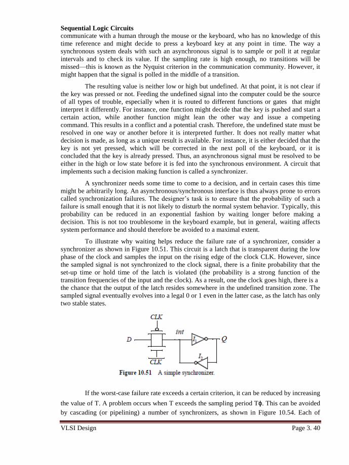
Sequential Logic Circuits
VLSI Design Page 3. 40
communicate with a human through the mouse or the keyboard, who has no knowledge of this
time reference and might decide to press a keyboard key at any point in time. The way a
synchronous system deals with such an asynchronous signal is to sample or poll it at regular
intervals and to check its value. If the sampling rate is high enough, no transitions will be
missed—this is known as the Nyquist criterion in the communication community. However, it
might happen that the signal is polled in the middle of a transition.
The resulting value is neither low or high but undefined. At that point, it is not clear if
the key was pressed or not. Feeding the undefined signal into the computer could be the source
of all types of trouble, especially when it is routed to different functions or gates that might
interpret it differently. For instance, one function might decide that the key is pushed and start a
certain action, while another function might lean the other way and issue a competing
command. This results in a conflict and a potential crash. Therefore, the undefined state must be
resolved in one way or another before it is interpreted further. It does not really matter what
decision is made, as long as a unique result is available. For instance, it is either decided that the
key is not yet pressed, which will be corrected in the next poll of the keyboard, or it is
concluded that the key is already pressed. Thus, an asynchronous signal must be resolved to be
either in the high or low state before it is fed into the synchronous environment. A circuit that
implements such a decision making function is called a synchronizer.
A synchronizer needs some time to come to a decision, and in certain cases this time
might be arbitrarily long. An asynchronous/synchronous interface is thus always prone to errors
called synchronization failures. The designer’s task is to ensure that the probability of such a
failure is small enough that it is not likely to disturb the normal system behavior. Typically, this
probability can be reduced in an exponential fashion by waiting longer before making a
decision. This is not too troublesome in the keyboard example, but in general, waiting affects
system performance and should therefore be avoided to a maximal extent.
To illustrate why waiting helps reduce the failure rate of a synchronizer, consider a
synchronizer as shown in Figure 10.51. This circuit is a latch that is transparent during the low
phase of the clock and samples the input on the rising edge of the clock CLK. However, since
the sampled signal is not synchronized to the clock signal, there is a finite probability that the
set-up time or hold time of the latch is violated (the probability is a strong function of the
transition frequencies of the input and the clock). As a result, one the clock goes high, there is a
the chance that the output of the latch resides somewhere in the undefined transition zone. The
sampled signal eventually evolves into a legal 0 or 1 even in the latter case, as the latch has only
two stable states.
If the worst-case failure rate exceeds a certain criterion, it can be reduced by increasing
the value of T. A problem occurs when T exceeds the sampling period Tɸ. This can be avoided
by cascading (or pipelining) a number of synchronizers, as shown in Figure 10.54. Each of
www.AllAbtEngg.com
AllAbtEngg Android Application for Anna University, Polytechnic & School
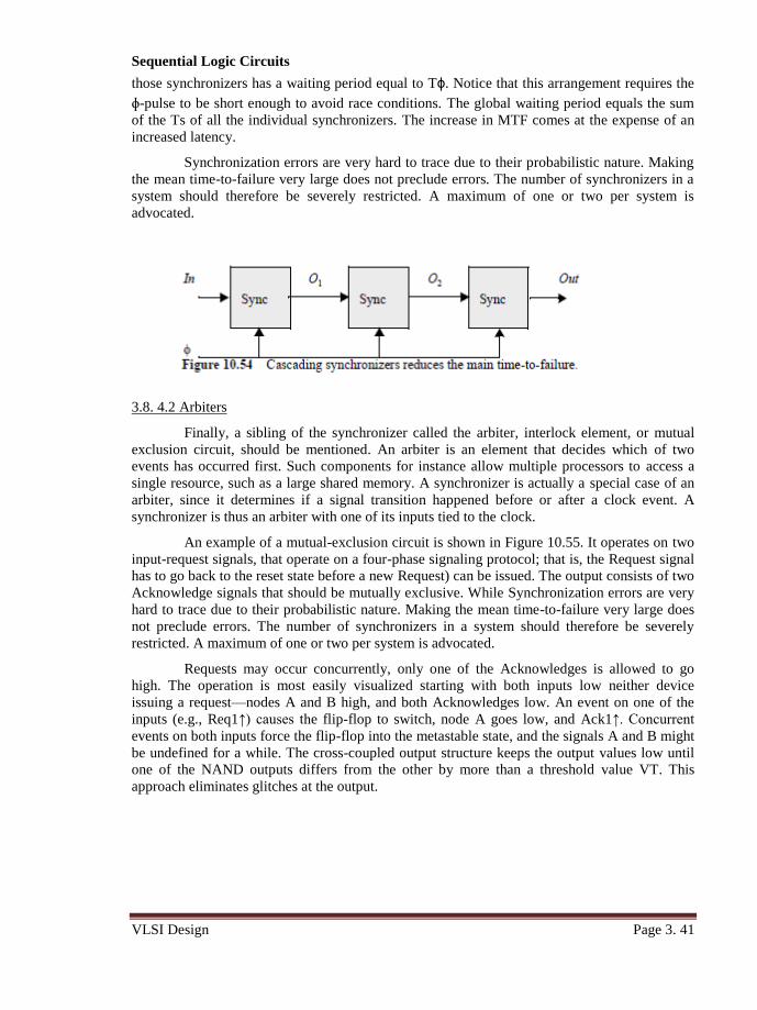
Sequential Logic Circuits
VLSI Design Page 3. 41
those synchronizers has a waiting period equal to Tɸ. Notice that this arrangement requires the
ɸ-pulse to be short enough to avoid race conditions. The global waiting period equals the sum
of the Ts of all the individual synchronizers. The increase in MTF comes at the expense of an
increased latency.
Synchronization errors are very hard to trace due to their probabilistic nature. Making
the mean time-to-failure very large does not preclude errors. The number of synchronizers in a
system should therefore be severely restricted. A maximum of one or two per system is
advocated.
3.8. 4.2 Arbiters
Finally, a sibling of the synchronizer called the arbiter, interlock element, or mutual
exclusion circuit, should be mentioned. An arbiter is an element that decides which of two
events has occurred first. Such components for instance allow multiple processors to access a
single resource, such as a large shared memory. A synchronizer is actually a special case of an
arbiter, since it determines if a signal transition happened before or after a clock event. A
synchronizer is thus an arbiter with one of its inputs tied to the clock.
An example of a mutual-exclusion circuit is shown in Figure 10.55. It operates on two
input-request signals, that operate on a four-phase signaling protocol; that is, the Request signal
has to go back to the reset state before a new Request) can be issued. The output consists of two
Acknowledge signals that should be mutually exclusive. While Synchronization errors are very
hard to trace due to their probabilistic nature. Making the mean time-to-failure very large does
not preclude errors. The number of synchronizers in a system should therefore be severely
restricted. A maximum of one or two per system is advocated.
Requests may occur concurrently, only one of the Acknowledges is allowed to go
high. The operation is most easily visualized starting with both inputs low neither device
issuing a request—nodes A and B high, and both Acknowledges low. An event on one of the
inputs (e.g., Req1↑) causes the flip-flop to switch, node A goes low, and Ack1↑. Concurrent
events on both inputs force the flip-flop into the metastable state, and the signals A and B might
be undefined for a while. The cross-coupled output structure keeps the output values low until
one of the NAND outputs differs from the other by more than a threshold value VT. This
approach eliminates glitches at the output.
www.AllAbtEngg.com
AllAbtEngg Android Application for Anna University, Polytechnic & School
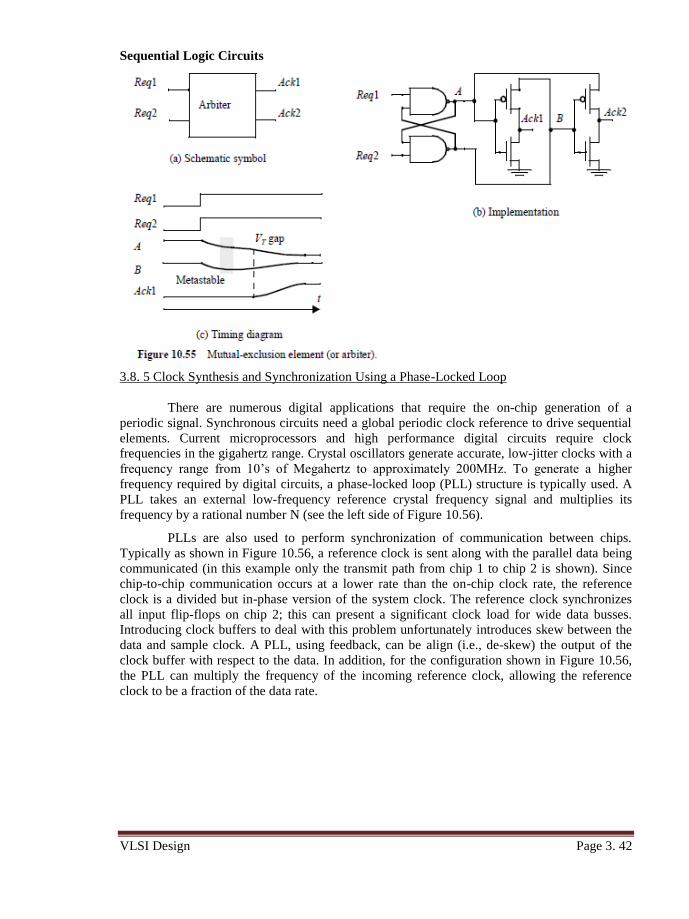
Sequential Logic Circuits
VLSI Design Page 3. 42
3.8. 5 Clock Synthesis and Synchronization Using a Phase-Locked Loop
There are numerous digital applications that require the on-chip generation of a
periodic signal. Synchronous circuits need a global periodic clock reference to drive sequential
elements. Current microprocessors and high performance digital circuits require clock
frequencies in the gigahertz range. Crystal oscillators generate accurate, low-jitter clocks with a
frequency range from 10’s of Megahertz to approximately 200MHz. To generate a higher
frequency required by digital circuits, a phase-locked loop (PLL) structure is typically used. A
PLL takes an external low-frequency reference crystal frequency signal and multiplies its
frequency by a rational number N (see the left side of Figure 10.56).
PLLs are also used to perform synchronization of communication between chips.
Typically as shown in Figure 10.56, a reference clock is sent along with the parallel data being
communicated (in this example only the transmit path from chip 1 to chip 2 is shown). Since
chip-to-chip communication occurs at a lower rate than the on-chip clock rate, the reference
clock is a divided but in-phase version of the system clock. The reference clock synchronizes
all input flip-flops on chip 2; this can present a significant clock load for wide data busses.
Introducing clock buffers to deal with this problem unfortunately introduces skew between the
data and sample clock. A PLL, using feedback, can be align (i.e., de-skew) the output of the
clock buffer with respect to the data. In addition, for the configuration shown in Figure 10.56,
the PLL can multiply the frequency of the incoming reference clock, allowing the reference
clock to be a fraction of the data rate.
www.AllAbtEngg.com
AllAbtEngg Android Application for Anna University, Polytechnic & School
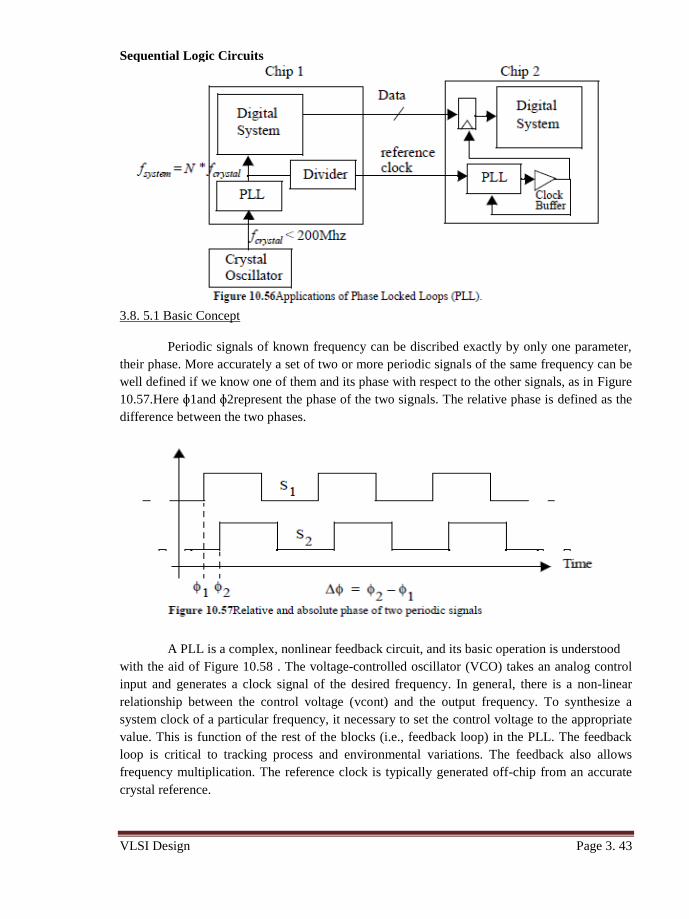
Sequential Logic Circuits
VLSI Design Page 3. 43
3.8. 5.1 Basic Concept
Periodic signals of known frequency can be discribed exactly by only one parameter,
their phase. More accurately a set of two or more periodic signals of the same frequency can be
well defined if we know one of them and its phase with respect to the other signals, as in Figure
10.57.Here ɸ1and ɸ2represent the phase of the two signals. The relative phase is defined as the
difference between the two phases.
A PLL is a complex, nonlinear feedback circuit, and its basic operation is understood
with the aid of Figure 10.58 . The voltage-controlled oscillator (VCO) takes an analog control
input and generates a clock signal of the desired frequency. In general, there is a non-linear
relationship between the control voltage (vcont) and the output frequency. To synthesize a
system clock of a particular frequency, it necessary to set the control voltage to the appropriate
value. This is function of the rest of the blocks (i.e., feedback loop) in the PLL. The feedback
loop is critical to tracking process and environmental variations. The feedback also allows
frequency multiplication. The reference clock is typically generated off-chip from an accurate
crystal reference.
www.AllAbtEngg.com
AllAbtEngg Android Application for Anna University, Polytechnic & School
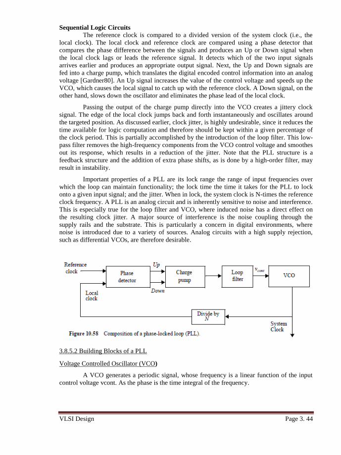
Sequential Logic Circuits
VLSI Design Page 3. 44
The reference clock is compared to a divided version of the system clock (i.e., the
local clock). The local clock and reference clock are compared using a phase detector that
compares the phase difference between the signals and produces an Up or Down signal when
the local clock lags or leads the reference signal. It detects which of the two input signals
arrives earlier and produces an appropriate output signal. Next, the Up and Down signals are
fed into a charge pump, which translates the digital encoded control information into an analog
voltage [Gardner80]. An Up signal increases the value of the control voltage and speeds up the
VCO, which causes the local signal to catch up with the reference clock. A Down signal, on the
other hand, slows down the oscillator and eliminates the phase lead of the local clock.
Passing the output of the charge pump directly into the VCO creates a jittery clock
signal. The edge of the local clock jumps back and forth instantaneously and oscillates around
the targeted position. As discussed earlier, clock jitter, is highly undesirable, since it reduces the
time available for logic computation and therefore should be kept within a given percentage of
the clock period. This is partially accomplished by the introduction of the loop filter. This low-
pass filter removes the high-frequency components from the VCO control voltage and smoothes
out its response, which results in a reduction of the jitter. Note that the PLL structure is a
feedback structure and the addition of extra phase shifts, as is done by a high-order filter, may
result in instability.
Important properties of a PLL are its lock range the range of input frequencies over
which the loop can maintain functionality; the lock time the time it takes for the PLL to lock
onto a given input signal; and the jitter. When in lock, the system clock is N-times the reference
clock frequency. A PLL is an analog circuit and is inherently sensitive to noise and interference.
This is especially true for the loop filter and VCO, where induced noise has a direct effect on
the resulting clock jitter. A major source of interference is the noise coupling through the
supply rails and the substrate. This is particularly a concern in digital environments, where
noise is introduced due to a variety of sources. Analog circuits with a high supply rejection,
such as differential VCOs, are therefore desirable.
3.8.5.2 Building Blocks of a PLL
Voltage Controlled Oscillator (VCO)
A VCO generates a periodic signal, whose frequency is a linear function of the input
control voltage vcont. As the phase is the time integral of the frequency.
www.AllAbtEngg.com
AllAbtEngg Android Application for Anna University, Polytechnic & School
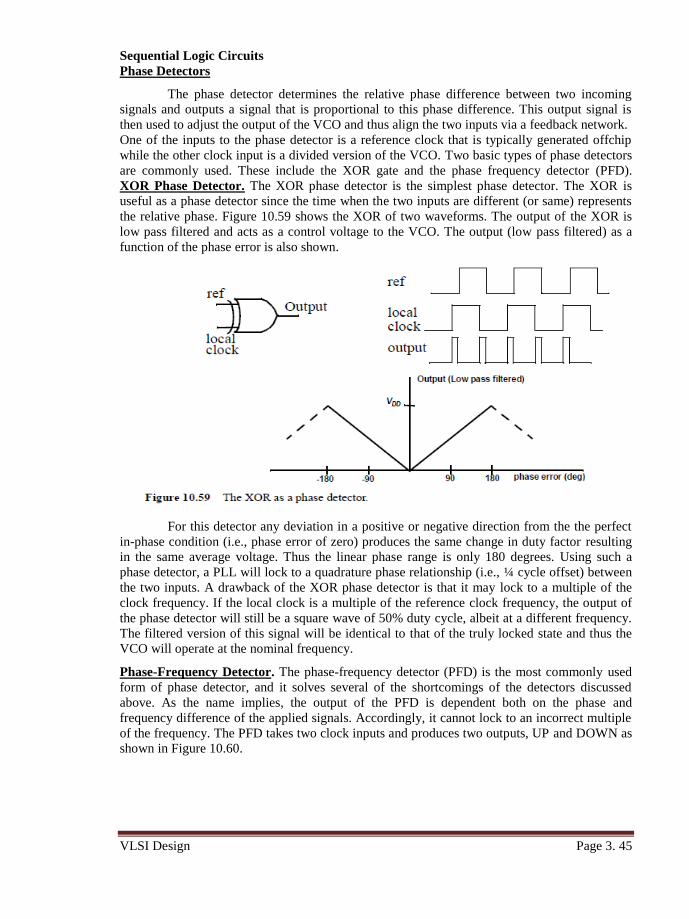
Sequential Logic Circuits
VLSI Design Page 3. 45
Phase Detectors
The phase detector determines the relative phase difference between two incoming
signals and outputs a signal that is proportional to this phase difference. This output signal is
then used to adjust the output of the VCO and thus align the two inputs via a feedback network.
One of the inputs to the phase detector is a reference clock that is typically generated offchip
while the other clock input is a divided version of the VCO. Two basic types of phase detectors
are commonly used. These include the XOR gate and the phase frequency detector (PFD).
XOR Phase Detector. The XOR phase detector is the simplest phase detector. The XOR is
useful as a phase detector since the time when the two inputs are different (or same) represents
the relative phase. Figure 10.59 shows the XOR of two waveforms. The output of the XOR is
low pass filtered and acts as a control voltage to the VCO. The output (low pass filtered) as a
function of the phase error is also shown.
For this detector any deviation in a positive or negative direction from the the perfect
in-phase condition (i.e., phase error of zero) produces the same change in duty factor resulting
in the same average voltage. Thus the linear phase range is only 180 degrees. Using such a
phase detector, a PLL will lock to a quadrature phase relationship (i.e., ¼ cycle offset) between
the two inputs. A drawback of the XOR phase detector is that it may lock to a multiple of the
clock frequency. If the local clock is a multiple of the reference clock frequency, the output of
the phase detector will still be a square wave of 50% duty cycle, albeit at a different frequency.
The filtered version of this signal will be identical to that of the truly locked state and thus the
VCO will operate at the nominal frequency.
Phase-Frequency Detector. The phase-frequency detector (PFD) is the most commonly used
form of phase detector, and it solves several of the shortcomings of the detectors discussed
above. As the name implies, the output of the PFD is dependent both on the phase and
frequency difference of the applied signals. Accordingly, it cannot lock to an incorrect multiple
of the frequency. The PFD takes two clock inputs and produces two outputs, UP and DOWN as
shown in Figure 10.60.
www.AllAbtEngg.com
AllAbtEngg Android Application for Anna University, Polytechnic & School
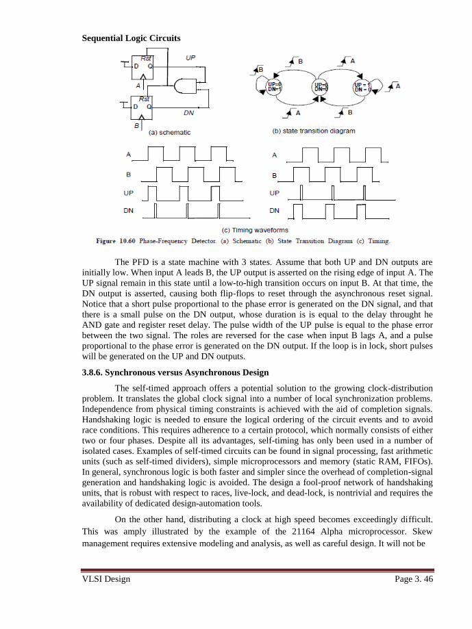
Sequential Logic Circuits
VLSI Design Page 3. 46
The PFD is a state machine with 3 states. Assume that both UP and DN outputs are
initially low. When input A leads B, the UP output is asserted on the rising edge of input A. The
UP signal remain in this state until a low-to-high transition occurs on input B. At that time, the
DN output is asserted, causing both flip-flops to reset through the asynchronous reset signal.
Notice that a short pulse proportional to the phase error is generated on the DN signal, and that
there is a small pulse on the DN output, whose duration is is equal to the delay throught he
AND gate and register reset delay. The pulse width of the UP pulse is equal to the phase error
between the two signal. The roles are reversed for the case when input B lags A, and a pulse
proportional to the phase error is generated on the DN output. If the loop is in lock, short pulses
will be generated on the UP and DN outputs.
3.8.6. Synchronous versus Asynchronous Design
The self-timed approach offers a potential solution to the growing clock-distribution
problem. It translates the global clock signal into a number of local synchronization problems.
Independence from physical timing constraints is achieved with the aid of completion signals.
Handshaking logic is needed to ensure the logical ordering of the circuit events and to avoid
race conditions. This requires adherence to a certain protocol, which normally consists of either
two or four phases. Despite all its advantages, self-timing has only been used in a number of
isolated cases. Examples of self-timed circuits can be found in signal processing, fast arithmetic
units (such as self-timed dividers), simple microprocessors and memory (static RAM, FIFOs).
In general, synchronous logic is both faster and simpler since the overhead of completion-signal
generation and handshaking logic is avoided. The design a fool-proof network of handshaking
units, that is robust with respect to races, live-lock, and dead-lock, is nontrivial and requires the
availability of dedicated design-automation tools.
On the other hand, distributing a clock at high speed becomes exceedingly difficult.
This was amply illustrated by the example of the 21164 Alpha microprocessor. Skew
management requires extensive modeling and analysis, as well as careful design. It will not be
www.AllAbtEngg.com
AllAbtEngg Android Application for Anna University, Polytechnic & School
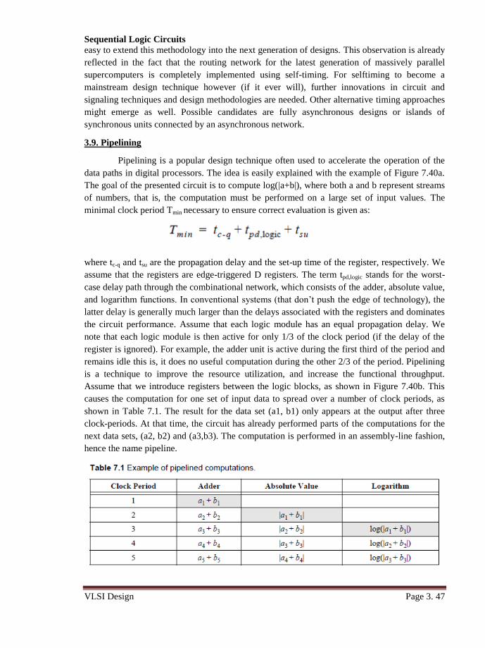
Sequential Logic Circuits
VLSI Design Page 3. 47
easy to extend this methodology into the next generation of designs. This observation is already
reflected in the fact that the routing network for the latest generation of massively parallel
supercomputers is completely implemented using self-timing. For selftiming to become a
mainstream design technique however (if it ever will), further innovations in circuit and
signaling techniques and design methodologies are needed. Other alternative timing approaches
might emerge as well. Possible candidates are fully asynchronous designs or islands of
synchronous units connected by an asynchronous network.
3.9. Pipelining
Pipelining is a popular design technique often used to accelerate the operation of the
data paths in digital processors. The idea is easily explained with the example of Figure 7.40a.
The goal of the presented circuit is to compute log(|a+b|), where both a and b represent streams
of numbers, that is, the computation must be performed on a large set of input values. The
minimal clock period Tmin necessary to ensure correct evaluation is given as:
where tc-q and tsu are the propagation delay and the set-up time of the register, respectively. We
assume that the registers are edge-triggered D registers. The term tpd,logic stands for the worst-
case delay path through the combinational network, which consists of the adder, absolute value,
and logarithm functions. In conventional systems (that don’t push the edge of technology), the
latter delay is generally much larger than the delays associated with the registers and dominates
the circuit performance. Assume that each logic module has an equal propagation delay. We
note that each logic module is then active for only 1/3 of the clock period (if the delay of the
register is ignored). For example, the adder unit is active during the first third of the period and
remains idle this is, it does no useful computation during the other 2/3 of the period. Pipelining
is a technique to improve the resource utilization, and increase the functional throughput.
Assume that we introduce registers between the logic blocks, as shown in Figure 7.40b. This
causes the computation for one set of input data to spread over a number of clock periods, as
shown in Table 7.1. The result for the data set (a1, b1) only appears at the output after three
clock-periods. At that time, the circuit has already performed parts of the computations for the
next data sets, (a2, b2) and (a3,b3). The computation is performed in an assembly-line fashion,
hence the name pipeline.
www.AllAbtEngg.com
AllAbtEngg Android Application for Anna University, Polytechnic & School

Sequential Logic Circuits
VLSI Design Page 3. 48
The advantage of pipelined operation becomes apparent when examining the minimum
clock period of the modified circuit. The combinational circuit block has been partitioned into
three sections, each of which has a smaller propagation delay than the original function. This
effectively reduces the value of the minimum allowable clock period:
Suppose that all logic blocks have approximately the same propagation delay, and that
the register overhead is small with respect to the logic delays. The pipelined network
outperforms the original circuit by a factor of three under these assumptions, or Tmin,pipe= Tmin/3.
The increased performance comes at the relatively small cost of two additional registers, and an
increased latency.2 This explains why pipelining is popular in the implementation of very high-
performance data paths.
3.9.1 Latch- vs. Register-Based Pipelines
Pipelined circuits can be constructed using level-sensitive latches instead of edge-
triggered registers. Consider the pipelined circuit of Figure 7.41. The pipeline system is
implemented based on pass-transistor-based positive and negative latches instead of edge
triggered registers. That is, logic is introduced between the master and slave latches of a master-
slave system. In the following discussion, we use without loss of generality the CLK-CLK
notation to denote a two-phase clock system.
www.AllAbtEngg.com
AllAbtEngg Android Application for Anna University, Polytechnic & School
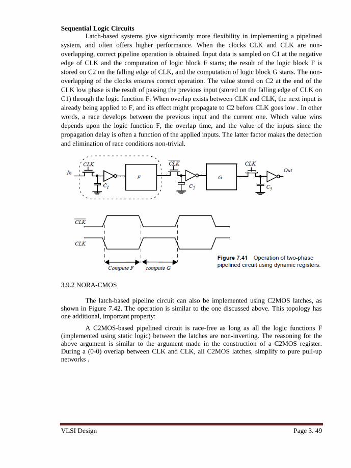
Sequential Logic Circuits
VLSI Design Page 3. 49
Latch-based systems give significantly more flexibility in implementing a pipelined
system, and often offers higher performance. When the clocks CLK and CLK are non-
overlapping, correct pipeline operation is obtained. Input data is sampled on C1 at the negative
edge of CLK and the computation of logic block F starts; the result of the logic block F is
stored on C2 on the falling edge of CLK, and the computation of logic block G starts. The non-
overlapping of the clocks ensures correct operation. The value stored on C2 at the end of the
CLK low phase is the result of passing the previous input (stored on the falling edge of CLK on
C1) through the logic function F. When overlap exists between CLK and CLK, the next input is
already being applied to F, and its effect might propagate to C2 before CLK goes low . In other
words, a race develops between the previous input and the current one. Which value wins
depends upon the logic function F, the overlap time, and the value of the inputs since the
propagation delay is often a function of the applied inputs. The latter factor makes the detection
and elimination of race conditions non-trivial.
3.9.2 NORA-CMOS
The latch-based pipeline circuit can also be implemented using C2MOS latches, as
shown in Figure 7.42. The operation is similar to the one discussed above. This topology has
one additional, important property:
A C2MOS-based pipelined circuit is race-free as long as all the logic functions F
(implemented using static logic) between the latches are non-inverting. The reasoning for the
above argument is similar to the argument made in the construction of a C2MOS register.
During a (0-0) overlap between CLK and CLK, all C2MOS latches, simplify to pure pull-up
networks .
www.AllAbtEngg.com
AllAbtEngg Android Application for Anna University, Polytechnic & School
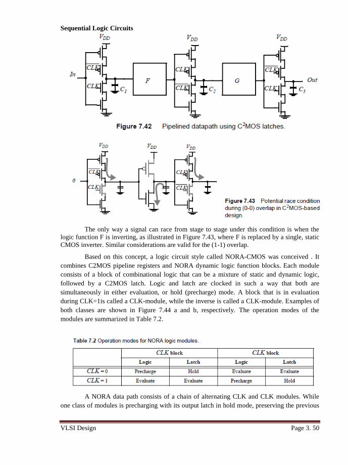
Sequential Logic Circuits
VLSI Design Page 3. 50
The only way a signal can race from stage to stage under this condition is when the
logic function F is inverting, as illustrated in Figure 7.43, where F is replaced by a single, static
CMOS inverter. Similar considerations are valid for the (1-1) overlap.
Based on this concept, a logic circuit style called NORA-CMOS was conceived . It
combines C2MOS pipeline registers and NORA dynamic logic function blocks. Each module
consists of a block of combinational logic that can be a mixture of static and dynamic logic,
followed by a C2MOS latch. Logic and latch are clocked in such a way that both are
simultaneously in either evaluation, or hold (precharge) mode. A block that is in evaluation
during CLK=1is called a CLK-module, while the inverse is called a CLK-module. Examples of
both classes are shown in Figure 7.44 a and b, respectively. The operation modes of the
modules are summarized in Table 7.2.
A NORA data path consists of a chain of alternating CLK and CLK modules. While
one class of modules is precharging with its output latch in hold mode, preserving the previous
www.AllAbtEngg.com
AllAbtEngg Android Application for Anna University, Polytechnic & School
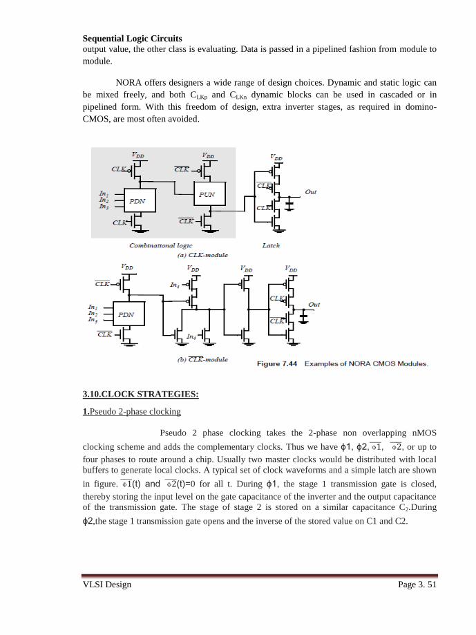
Sequential Logic Circuits
VLSI Design Page 3. 51
output value, the other class is evaluating. Data is passed in a pipelined fashion from module to
module.
NORA offers designers a wide range of design choices. Dynamic and static logic can
be mixed freely, and both CLKp and CLKn dynamic blocks can be used in cascaded or in
pipelined form. With this freedom of design, extra inverter stages, as required in domino-
CMOS, are most often avoided.
3.10.CLOCK STRATEGIES:
1.Pseudo 2-phase clocking
Pseudo 2 phase clocking takes the 2-phase non overlapping nMOS
clocking scheme and adds the complementary clocks. Thus we have ɸ1, ɸ2, ɸ1 , ɸ2 , or up to
four phases to route around a chip. Usually two master clocks would be distributed with local
buffers to generate local clocks. A typical set of clock waveforms and a simple latch are shown
in figure. ɸ1 (t) and ɸ2 (t)=0 for all t. During ɸ1, the stage 1 transmission gate is closed,
thereby storing the input level on the gate capacitance of the inverter and the output capacitance
of the transmission gate. The stage of stage 2 is stored on a similar capacitance C2.During
ɸ2,the stage 1 transmission gate opens and the inverse of the stored value on C1 and C2.
www.AllAbtEngg.com
AllAbtEngg Android Application for Anna University, Polytechnic & School
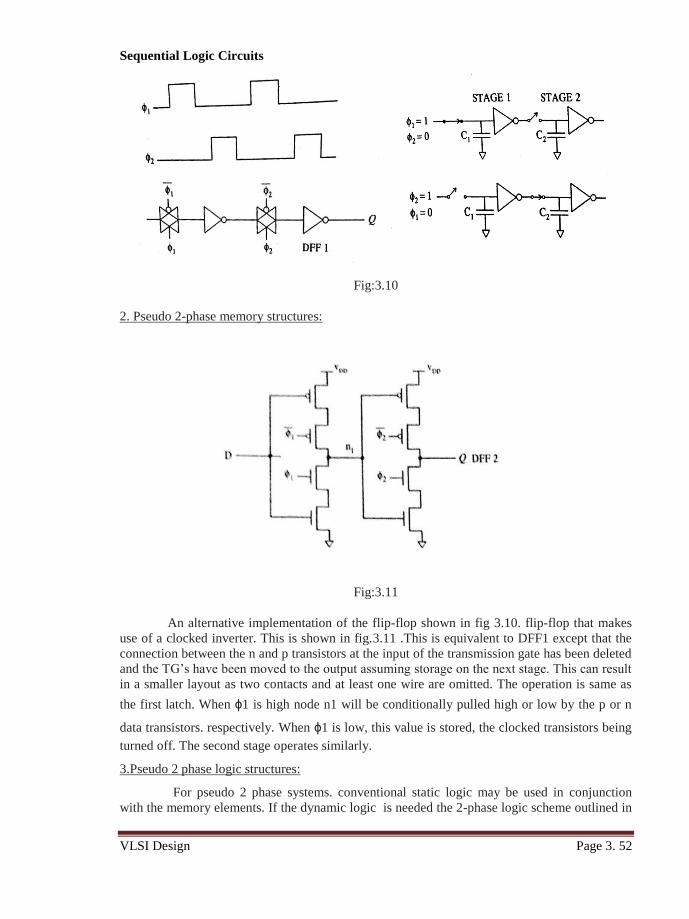
Sequential Logic Circuits
VLSI Design Page 3. 52
Fig:3.10
2. Pseudo 2-phase memory structures:
Fig:3.11
An alternative implementation of the flip-flop shown in fig 3.10. flip-flop that makes
use of a clocked inverter. This is shown in fig.3.11 .This is equivalent to DFF1 except that the
connection between the n and p transistors at the input of the transmission gate has been deleted
and the TG’s have been moved to the output assuming storage on the next stage. This can result
in a smaller layout as two contacts and at least one wire are omitted. The operation is same as
the first latch. When ɸ1 is high node n1 will be conditionally pulled high or low by the p or n
data transistors. respectively. When ɸ1 is low, this value is stored, the clocked transistors being
turned off. The second stage operates similarly.
3.Pseudo 2 phase logic structures:
For pseudo 2 phase systems. conventional static logic may be used in conjunction
with the memory elements. If the dynamic logic is needed the 2-phase logic scheme outlined in
www.AllAbtEngg.com
AllAbtEngg Android Application for Anna University, Polytechnic & School

Sequential Logic Circuits
VLSI Design Page 3. 53
fig 3.12 may be used. In this the first stage is pre charged during ɸ1 and evaluated during ɸ2.
While the first stage is evaluated, the second stage is pre charged and the first stage outputs are
stored on the second stage inputs. During ɸ1 the second stage is evaluated and latched in a
succeeding ɸ1 stage
4.Two phase clocking
In some situation it is desirable to redue the number of clock lines that are routed
around the chip.One approach is to use a 2-phase clock that uses a ɸ,∅ type arrangements.
5.Two phase memory structures
Applying this clocking strategies to the flip-flop used in the pseudo 2-phase clocking,
the structure in fig.3.13a is consructed.A clock race condition similar to that encountered in the
pseudo 2-phase latch that can arise in this structure.This is of course an accentuated case of
pseudo 2 phase skew mentioned previously.This effect is shown in fig. 3.13b.Considering ∅
delayed from ɸ,we see that the first transmission gate n-transistor can be turned on at the same
times as the second transmission gate n-transistor.Hence the value on the input can ripple
through the two transmission gates leading to invalid data storage.This problem means that
close attention must be paid to the clock distribution to minimize the clock skew.One method of
achieving this is shown in fig. 3.13c.A conventional clock buffer consisting of two inverters is
shown. The buffered ɸ clock will always be delayed with respect to the buffered ∅ clock. To
reduce this undesirable delay , the ɸ signal may be passed through a transmission gate to
equalize delay with respect to ∅ . The transmission gate should use similar sized transistors to
those used in the inverters.Subsequent buffers may also be used to keep the initial buffers
minimum size.
www.AllAbtEngg.com
AllAbtEngg Android Application for Anna University, Polytechnic & School
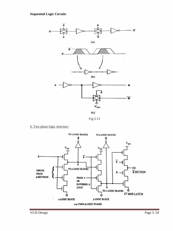
Sequential Logic Circuits
VLSI Design Page 3. 54
Fig:3.13
6. Two phase logic structure:
www.AllAbtEngg.com
AllAbtEngg Android Application for Anna University, Polytechnic & School
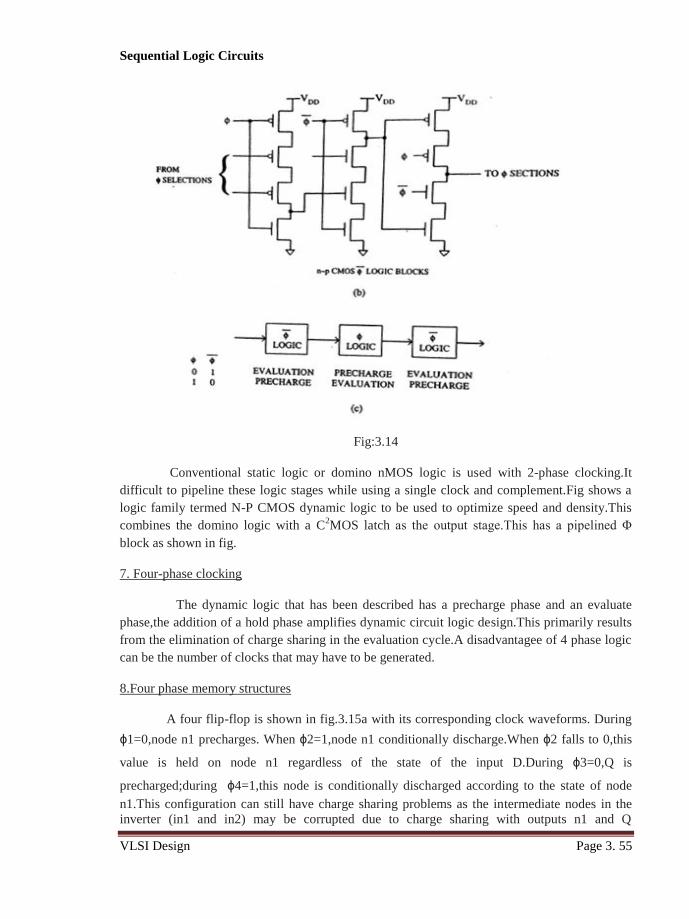
Sequential Logic Circuits
VLSI Design Page 3. 55
Fig:3.14
Conventional static logic or domino nMOS logic is used with 2-phase clocking.It
difficult to pipeline these logic stages while using a single clock and complement.Fig shows a
logic family termed N-P CMOS dynamic logic to be used to optimize speed and density.This
combines the domino logic with a C2MOS latch as the output stage.This has a pipelined Φ
block as shown in fig.
7. Four-phase clocking
The dynamic logic that has been described has a precharge phase and an evaluate
phase,the addition of a hold phase amplifies dynamic circuit logic design.This primarily results
from the elimination of charge sharing in the evaluation cycle.A disadvantagee of 4 phase logic
can be the number of clocks that may have to be generated.
8.Four phase memory structures
A four flip-flop is shown in fig.3.15a with its corresponding clock waveforms. During
ɸ1=0,node n1 precharges. When ɸ2=1,node n1 conditionally discharge.When ɸ2 falls to 0,this
value is held on node n1 regardless of the state of the input D.During ɸ3=0,Q is
precharged;during ɸ4=1,this node is conditionally discharged according to the state of node
n1.This configuration can still have charge sharing problems as the intermediate nodes in the
inverter (in1 and in2) may be corrupted due to charge sharing with outputs n1 and Q
www.AllAbtEngg.com
AllAbtEngg Android Application for Anna University, Polytechnic & School

Sequential Logic Circuits
VLSI Design Page 3. 56
,respectively. This is solved by altering the clock waveforms so that ɸ2 is actually ɸ12 and ɸ4
is ɸ34. As shown in fig.3.15b. with these clocking waveforms the intermediate nodes are
precharged uniformly.
Fig:3.15
9.Four phase logic structures:
The main purpose in adopting a 4-phase clocking strategies is to enable the 4-phase
logic gates to be built. The fact that no more clock lines are needed than for pseudo 2-phase
clocking if certain 4-phase structures are used.
Fig:3.16
www.AllAbtEngg.com
AllAbtEngg Android Application for Anna University, Polytechnic & School
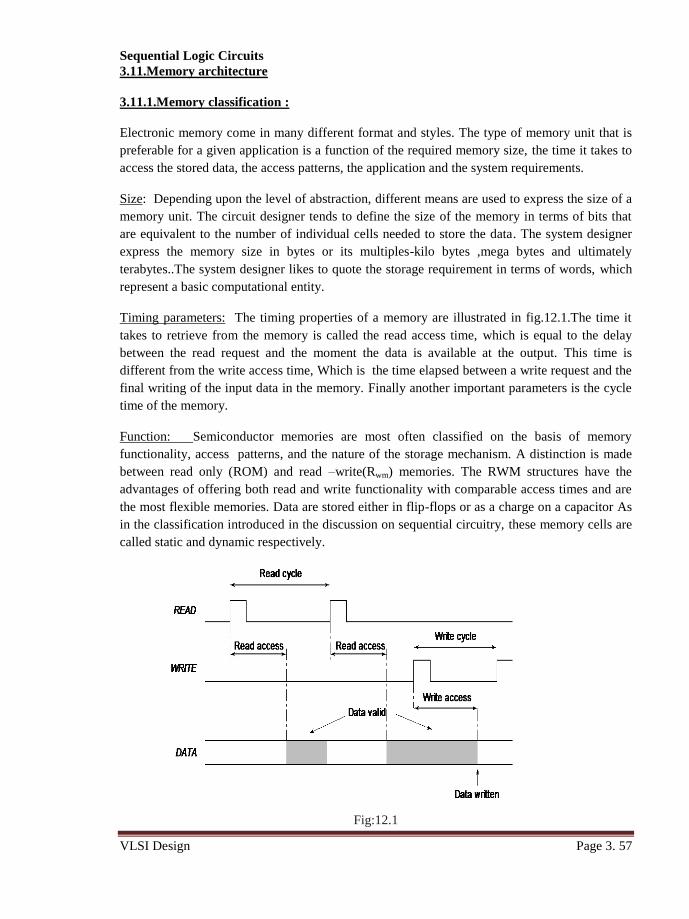
Sequential Logic Circuits
VLSI Design Page 3. 57
3.11.Memory architecture
3.11.1.Memory classification :
Electronic memory come in many different format and styles. The type of memory unit that is
preferable for a given application is a function of the required memory size, the time it takes to
access the stored data, the access patterns, the application and the system requirements.
Size: Depending upon the level of abstraction, different means are used to express the size of a
memory unit. The circuit designer tends to define the size of the memory in terms of bits that
are equivalent to the number of individual cells needed to store the data. The system designer
express the memory size in bytes or its multiples-kilo bytes ,mega bytes and ultimately
terabytes..The system designer likes to quote the storage requirement in terms of words, which
represent a basic computational entity.
Timing parameters: The timing properties of a memory are illustrated in fig.12.1.The time it
takes to retrieve from the memory is called the read access time, which is equal to the delay
between the read request and the moment the data is available at the output. This time is
different from the write access time, Which is the time elapsed between a write request and the
final writing of the input data in the memory. Finally another important parameters is the cycle
time of the memory.
Function: Semiconductor memories are most often classified on the basis of memory
functionality, access patterns, and the nature of the storage mechanism. A distinction is made
between read only (ROM) and read –write(Rwm) memories. The RWM structures have the
advantages of offering both read and write functionality with comparable access times and are
the most flexible memories. Data are stored either in flip-flops or as a charge on a capacitor As
in the classification introduced in the discussion on sequential circuitry, these memory cells are
called static and dynamic respectively.
Fig:12.1
www.AllAbtEngg.com
AllAbtEngg Android Application for Anna University, Polytechnic & School
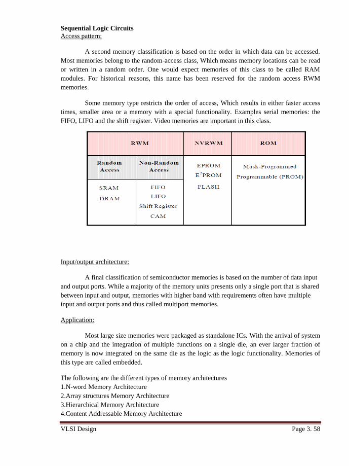
Sequential Logic Circuits
VLSI Design Page 3. 58
Access pattern:
A second memory classification is based on the order in which data can be accessed.
Most memories belong to the random-access class, Which means memory locations can be read
or written in a random order. One would expect memories of this class to be called RAM
modules. For historical reasons, this name has been reserved for the random access RWM
memories.
Some memory type restricts the order of access, Which results in either faster access
times, smaller area or a memory with a special functionality. Examples serial memories: the
FIFO, LIFO and the shift register. Video memories are important in this class.
Input/output architecture:
A final classification of semiconductor memories is based on the number of data input
and output ports. While a majority of the memory units presents only a single port that is shared
between input and output, memories with higher band with requirements often have multiple
input and output ports and thus called multiport memories.
Application:
Most large size memories were packaged as standalone ICs. With the arrival of system
on a chip and the integration of multiple functions on a single die, an ever larger fraction of
memory is now integrated on the same die as the logic as the logic functionality. Memories of
this type are called embedded.
The following are the different types of memory architectures
1.N-word Memory Architecture
2.Array structures Memory Architecture
3.Hierarchical Memory Architecture
4.Content Addressable Memory Architecture
www.AllAbtEngg.com
AllAbtEngg Android Application for Anna University, Polytechnic & School
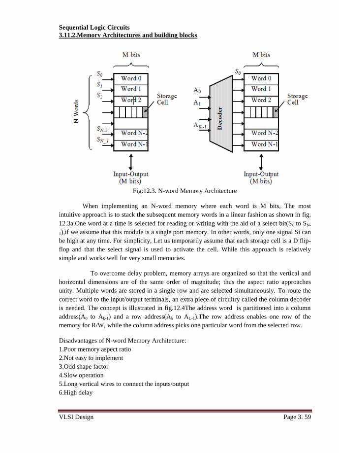
Sequential Logic Circuits
VLSI Design Page 3. 59
3.11.2.Memory Architectures and building blocks
Fig:12.3. N-word Memory Architecture
When implementing an N-word memory where each word is M bits, The most
intuitive approach is to stack the subsequent memory words in a linear fashion as shown in fig.
12.3a.One word at a time is selected for reading or writing with the aid of a select bit(S0 to SN-
1),if we assume that this module is a single port memory. In other words, only one signal Si can
be high at any time. For simplicity, Let us temporarily assume that each storage cell is a D flip-
flop and that the select signal is used to activate the cell. While this approach is relatively
simple and works well for very small memories.
To overcome delay problem, memory arrays are organized so that the vertical and
horizontal dimensions are of the same order of magnitude; thus the aspect ratio approaches
unity. Multiple words are stored in a single row and are selected simultaneously. To route the
correct word to the input/output terminals, an extra piece of circuitry called the column decoder
is needed. The concept is illustrated in fig.12.4The address word is partitioned into a column
address(A0 to Ak-1) and a row address(Ak to AL-1).The row address enables one row of the
memory for R/W, while the column address picks one particular word from the selected row.
Disadvantages of N-word Memory Architecture:
1.Poor memory aspect ratio
2.Not easy to implement
3.Odd shape factor
4.Slow operation
5.Long vertical wires to connect the inputs/output
6.High delay
www.AllAbtEngg.com
AllAbtEngg Android Application for Anna University, Polytechnic & School
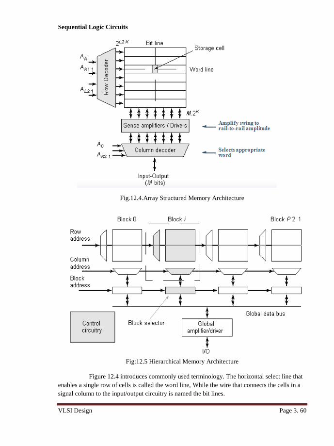
Sequential Logic Circuits
VLSI Design Page 3. 60
Fig.12.4.Array Structured Memory Architecture
Fig:12.5 Hierarchical Memory Architecture
Figure 12.4 introduces commonly used terminology. The horizontal select line that
enables a single row of cells is called the word line, While the wire that connects the cells in a
signal column to the input/output circuitry is named the bit lines.
www.AllAbtEngg.com
AllAbtEngg Android Application for Anna University, Polytechnic & School
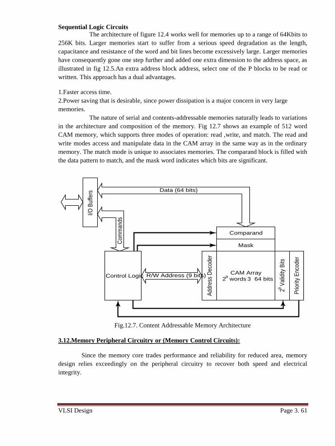
Sequential Logic Circuits
VLSI Design Page 3. 61
Add
ress
Dec
oder
Data (64 bits)
I/O B
uffe
rs
Comparand
CAM Array2
9 words 3 64 bits
Mask
Control Logic R/W Address (9 bits)
Com
man
ds
29 Val
idity
Bits
Prio
rity
Enc
oder
The architecture of figure 12.4 works well for memories up to a range of 64Kbits to
256K bits. Larger memories start to suffer from a serious speed degradation as the length,
capacitance and resistance of the word and bit lines become excessively large. Larger memories
have consequently gone one step further and added one extra dimension to the address space, as
illustrated in fig 12.5.An extra address block address, select one of the P blocks to be read or
written. This approach has a dual advantages.
1.Faster access time.
2.Power saving that is desirable, since power dissipation is a major concern in very large
memories.
The nature of serial and contents-addressable memories naturally leads to variations
in the architecture and composition of the memory. Fig 12.7 shows an example of 512 word
CAM memory, which supports three modes of operation: read ,write, and match. The read and
write modes access and manipulate data in the CAM array in the same way as in the ordinary
memory. The match mode is unique to associates memories. The comparand block is filled with
the data pattern to match, and the mask word indicates which bits are significant.
Fig.12.7. Content Addressable Memory Architecture
3.12.Memory Peripheral Circuitry or (Memory Control Circuits):
Since the memory core trades performance and reliability for reduced area, memory
design relies exceedingly on the peripheral circuitry to recover both speed and electrical
integrity.
www.AllAbtEngg.com
AllAbtEngg Android Application for Anna University, Polytechnic & School
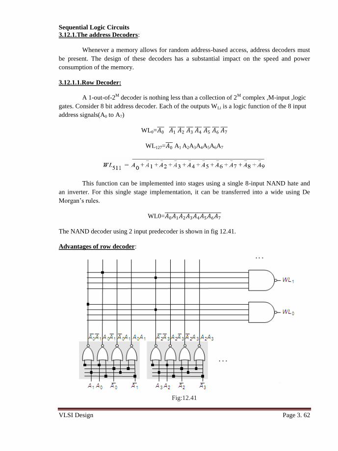
Sequential Logic Circuits
VLSI Design Page 3. 62
3.12.1.The address Decoders:
Whenever a memory allows for random address-based access, address decoders must
be present. The design of these decoders has a substantial impact on the speed and power
consumption of the memory.
3.12.1.1.Row Decoder:
A 1-out-of-2M
decoder is nothing less than a collection of 2M
complex ,M-input ,logic
gates. Consider 8 bit address decoder. Each of the outputs WLi is a logic function of the 8 input
address signals(A0 to A7)
WL0=𝐴0 𝐴1
𝐴2 𝐴3
𝐴4 𝐴5
𝐴6 𝐴7
WL127=𝐴0 A1 A2A3A4A5A6A7
This function can be implemented into stages using a single 8-input NAND hate and
an inverter. For this single stage implementation, it can be transferred into a wide using De
Morgan’s rules.
WL0=𝐴0𝐴1𝐴2𝐴3𝐴4𝐴5𝐴6𝐴7
The NAND decoder using 2 input predecoder is shown in fig 12.41.
Advantages of row decoder:
Fig:12.41
www.AllAbtEngg.com
AllAbtEngg Android Application for Anna University, Polytechnic & School
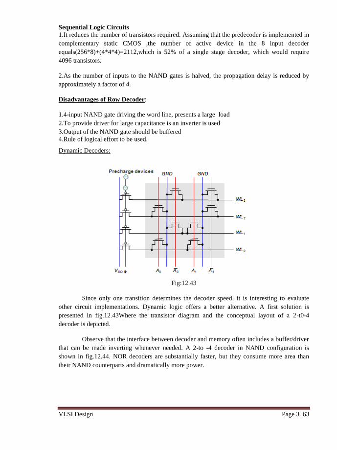
Sequential Logic Circuits
VLSI Design Page 3. 63
1.It reduces the number of transistors required. Assuming that the predecoder is implemented in
complementary static CMOS ,the number of active device in the 8 input decoder
equals(256*8)+(4*4*4)=2112,which is 52% of a single stage decoder, which would require
4096 transistors.
2.As the number of inputs to the NAND gates is halved, the propagation delay is reduced by
approximately a factor of 4.
Disadvantages of Row Decoder:
1.4-input NAND gate driving the word line, presents a large load
2.To provide driver for large capacitance is an inverter is used
3.Output of the NAND gate should be buffered
4.Rule of logical effort to be used.
Dynamic Decoders:
Fig:12.43
Since only one transition determines the decoder speed, it is interesting to evaluate
other circuit implementations. Dynamic logic offers a better alternative. A first solution is
presented in fig.12.43Where the transistor diagram and the conceptual layout of a 2-t0-4
decoder is depicted.
Observe that the interface between decoder and memory often includes a buffer/driver
that can be made inverting whenever needed. A 2-to -4 decoder in NAND configuration is
shown in fig.12.44. NOR decoders are substantially faster, but they consume more area than
their NAND counterparts and dramatically more power.
www.AllAbtEngg.com
AllAbtEngg Android Application for Anna University, Polytechnic & School
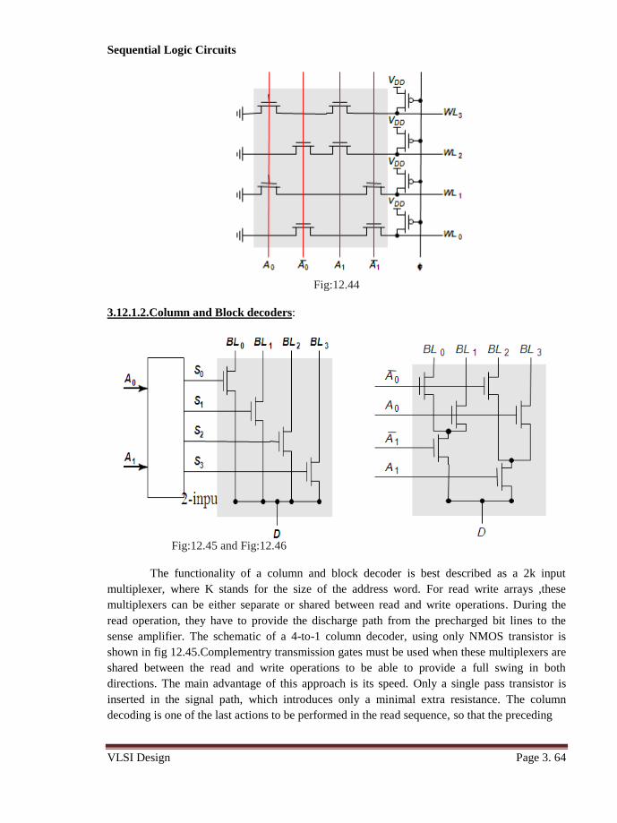
Sequential Logic Circuits
VLSI Design Page 3. 64
Fig:12.44
3.12.1.2.Column and Block decoders:
Fig:12.45 and Fig:12.46
The functionality of a column and block decoder is best described as a 2k input
multiplexer, where K stands for the size of the address word. For read write arrays ,these
multiplexers can be either separate or shared between read and write operations. During the
read operation, they have to provide the discharge path from the precharged bit lines to the
sense amplifier. The schematic of a 4-to-1 column decoder, using only NMOS transistor is
shown in fig 12.45.Complementry transmission gates must be used when these multiplexers are
shared between the read and write operations to be able to provide a full swing in both
directions. The main advantage of this approach is its speed. Only a single pass transistor is
inserted in the signal path, which introduces only a minimal extra resistance. The column
decoding is one of the last actions to be performed in the read sequence, so that the preceding
www.AllAbtEngg.com
AllAbtEngg Android Application for Anna University, Polytechnic & School
Sequential Logic Circuits
VLSI Design Page 3. 65
can be executed in parallel with other operations, such as memory access and sensing. The
disadvantages of the structure is its larger transistor count.A more efficient implementation is
offered by a tree decoder that used a binary reduction scheme, as shown in fig 12.46.The
number of devices is drastically reduced as shown in the following equation.
Ntree=2k+2
k-1+…+4+2=2*(2
k-1)
3.12.1.2 Decoders for Non-Random-Access Memories:
Memories that are not of the random access class do not need a full fledged decoder. In
a serial access memory, such as video –line memory, the decoder degenerates into M bit shift
register, with M the number of rows. Only one of the bits is high at a time and is called a
pointer. The pointer moves to the next position every time access is performed.
3.12.2.Sense Amplifier:
It perform Amplification, Delay Reduction ,Power reduction and signal restoration.
3.12.2.1.Differential Voltage Sensing Amplifiers:
A differential amplifier takes small signal differential inputs and amplifier them to a
large single encoded output. It is generally known that a differential approach presents
numerous advantages over its single ended counterpart-one of the most important being the
common-mode rejection. That is ,such an amplifier rejects noise that is equally rejected to both
inputs. This is especially attractive in memories where the exact value of the bit line signal
varies from die to die and even for different locations on a single die. The picture is further
complicated by the presence of multiple noise sources, such as switching spikes on the supply
voltages and capacitive cross talk between word and bit lines.
Fig 12.48 shows the most basic differential sense amplifier. Amplification is
accomplished with a single stage, based on the current mirroring concept. The input signals are
heavily loaded and driven by the SRAM memory cell. The swing on those lines is small as the
small memory cell drives a large capacitive load. The input signals are fed to the differential
input devices and transistors M3 and M4 act as an active current mirror load. T he amplifier is
conditioned by the sense amplifier enable signal, SE. Initially the inputs are precharged and
equalizes to a common value, while SE is low disabling the sensing circuits. Once the read
operation is initiated, one of the bit lines drops.SE is enabled when a sufficient differential
signal has been established, and the amplifier evaluates.
www.AllAbtEngg.com
AllAbtEngg Android Application for Anna University, Polytechnic & School
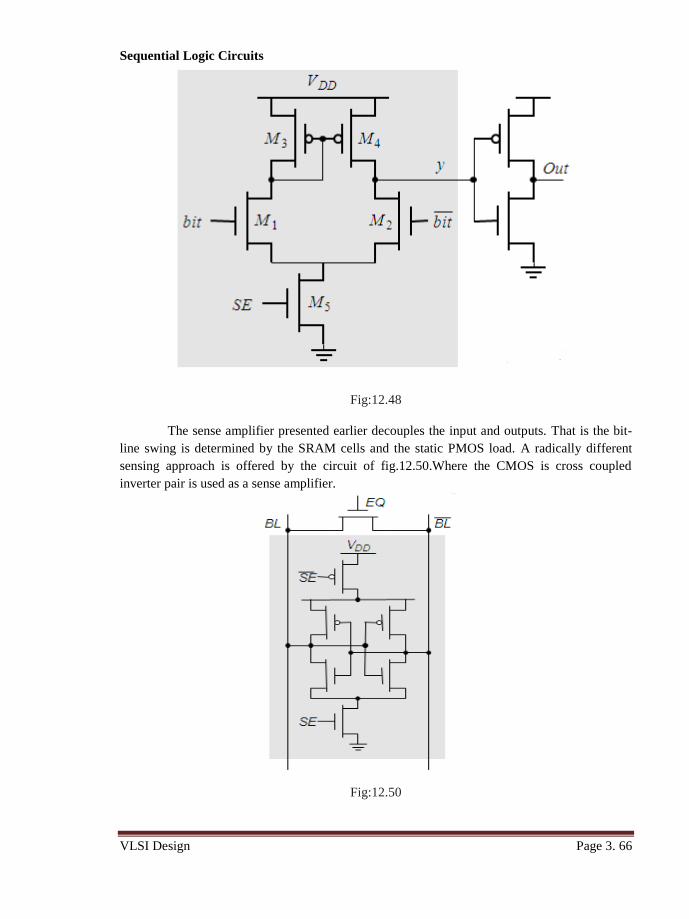
Sequential Logic Circuits
VLSI Design Page 3. 66
Fig:12.48
The sense amplifier presented earlier decouples the input and outputs. That is the bit-
line swing is determined by the SRAM cells and the static PMOS load. A radically different
sensing approach is offered by the circuit of fig.12.50.Where the CMOS is cross coupled
inverter pair is used as a sense amplifier.
Fig:12.50
www.AllAbtEngg.com
AllAbtEngg Android Application for Anna University, Polytechnic & School

Sequential Logic Circuits
VLSI Design Page 3. 67
A CMOS inverter exhibits a high gain when positioned in its transient region. To act
as a sense amplifier, the flip-flop is initialized in its metastable point by equalizing the bit lines.
A voltage difference is built over the bit lines in the course of the read process. Once a large
enough voltage gap is created ,the sense amplifier is enabled by raising SE. Depending upon
the input, the cross coupled pair transverse to one of its stable operation points. The transition is
swift as a result of the positive feedback.
3.12.2.2.Single –to –Differential Conversion:
Larger memories that are exceedingly prone to noise disturbances resort to
translating the single ended sensing problem into a differential one. The basic concept behind
the single to differential conversion is demonsrated in fig.12.53.A differential sense amplifier is
connected to a single –ended bit line on one side and a reference voltage, positioned between
the 0 and 1 levels, at the other end. Depending on the value of BL, the amplifier toggles in one
or the other direction. Creating a good reference source is not as easy as it sounds, since the
voltage level tends to vary from die to die or even over a single die. The reference source must
therefore track those variations.
Fig:12.53
3.12.3.Voltage References
Most memories requires some form of on-chip voltage generation. The operation of a
sophisticated memory requires a number of voltage references and supply levels, including
Boosted word line voltage, Half-VDD, Reduced internal supply and Negative substrate bias.
Voltage Down Converters:
Voltage down converters are used to create low internal supplies, allowing the
interface circuits to operate at higher voltages. The reduction of supply is in fact necessary to
avoid breakdown in the deep sub micron devices.Fig.12.56 shows the basic structure of a
voltage down converter .It is based on the operational amplifier. The circuit uses a large PMOS
output driver transistor to drive the load of the memory circuit. The circuit uses negative
feedback to set the output voltage VDL to the reference voltage.
www.AllAbtEngg.com
AllAbtEngg Android Application for Anna University, Polytechnic & School
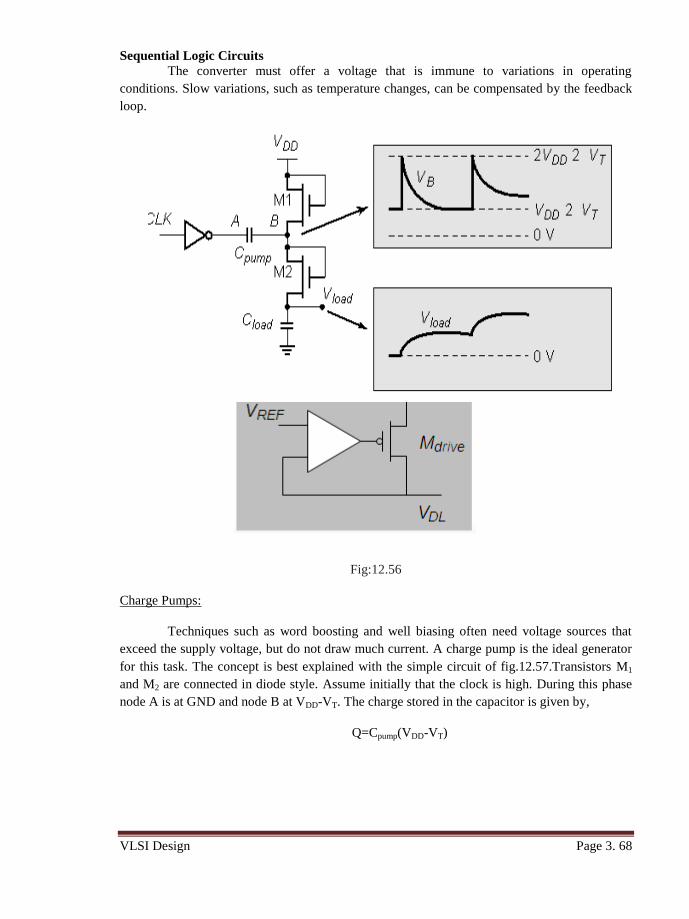
Sequential Logic Circuits
VLSI Design Page 3. 68
The converter must offer a voltage that is immune to variations in operating
conditions. Slow variations, such as temperature changes, can be compensated by the feedback
loop.
Fig:12.56
Charge Pumps:
Techniques such as word boosting and well biasing often need voltage sources that
exceed the supply voltage, but do not draw much current. A charge pump is the ideal generator
for this task. The concept is best explained with the simple circuit of fig.12.57.Transistors M1
and M2 are connected in diode style. Assume initially that the clock is high. During this phase
node A is at GND and node B at VDD-VT. The charge stored in the capacitor is given by,
Q=Cpump(VDD-VT)
www.AllAbtEngg.com
AllAbtEngg Android Application for Anna University, Polytechnic & School
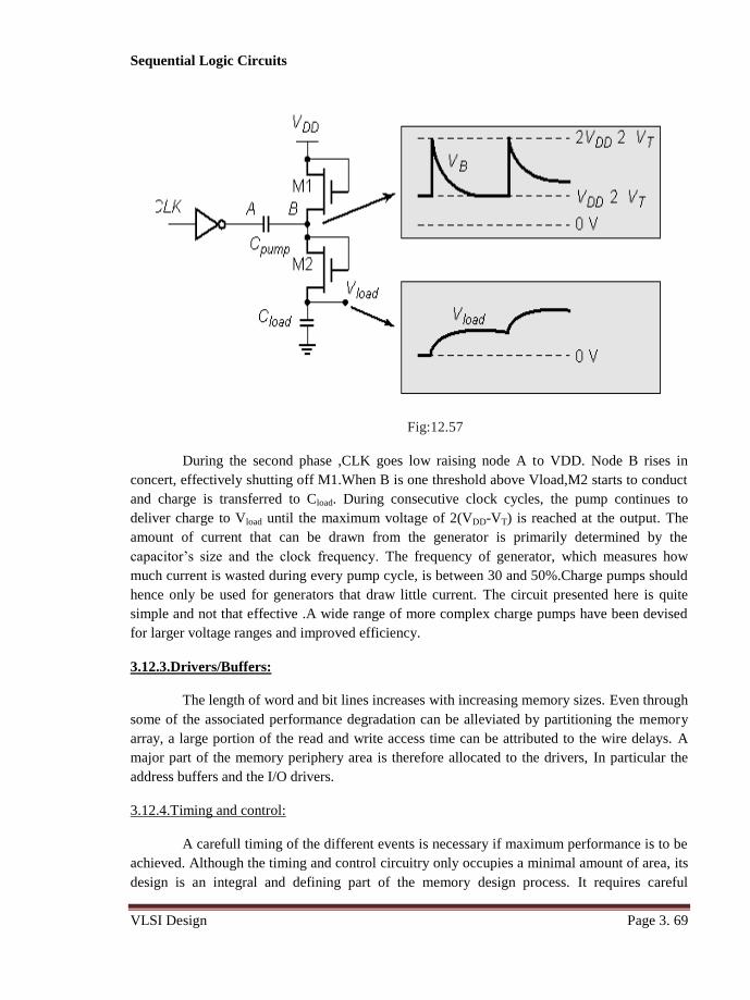
Sequential Logic Circuits
VLSI Design Page 3. 69
Fig:12.57
During the second phase ,CLK goes low raising node A to VDD. Node B rises in
concert, effectively shutting off M1.When B is one threshold above Vload,M2 starts to conduct
and charge is transferred to Cload. During consecutive clock cycles, the pump continues to
deliver charge to Vload until the maximum voltage of 2(VDD-VT) is reached at the output. The
amount of current that can be drawn from the generator is primarily determined by the
capacitor’s size and the clock frequency. The frequency of generator, which measures how
much current is wasted during every pump cycle, is between 30 and 50%.Charge pumps should
hence only be used for generators that draw little current. The circuit presented here is quite
simple and not that effective .A wide range of more complex charge pumps have been devised
for larger voltage ranges and improved efficiency.
3.12.3.Drivers/Buffers:
The length of word and bit lines increases with increasing memory sizes. Even through
some of the associated performance degradation can be alleviated by partitioning the memory
array, a large portion of the read and write access time can be attributed to the wire delays. A
major part of the memory periphery area is therefore allocated to the drivers, In particular the
address buffers and the I/O drivers.
3.12.4.Timing and control:
A carefull timing of the different events is necessary if maximum performance is to be
achieved. Although the timing and control circuitry only occupies a minimal amount of area, its
design is an integral and defining part of the memory design process. It requires careful
www.AllAbtEngg.com
AllAbtEngg Android Application for Anna University, Polytechnic & School
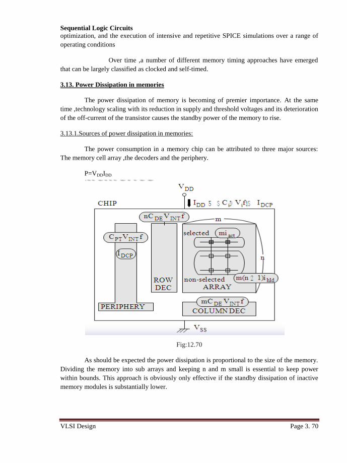
Sequential Logic Circuits
VLSI Design Page 3. 70
optimization, and the execution of intensive and repetitive SPICE simulations over a range of
operating conditions
Over time ,a number of different memory timing approaches have emerged
that can be largely classified as clocked and self-timed.
3.13. Power Dissipation in memories
The power dissipation of memory is becoming of premier importance. At the same
time ,technology scaling with its reduction in supply and threshold voltages and its deterioration
of the off-current of the transistor causes the standby power of the memory to rise.
3.13.1.Sources of power dissipation in memories:
The power consumption in a memory chip can be attributed to three major sources:
The memory cell array ,the decoders and the periphery.
P=VDDIDD
Fig:12.70
As should be expected the power dissipation is proportional to the size of the memory.
Dividing the memory into sub arrays and keeping n and m small is essential to keep power
within bounds. This approach is obviously only effective if the standby dissipation of inactive
memory modules is substantially lower.
www.AllAbtEngg.com
AllAbtEngg Android Application for Anna University, Polytechnic & School
Sequential Logic Circuits
VLSI Design Page 3. 71
3.13.2Partitioning of the memory:
Memory partitioning is accomplished by reducing m and/or n. By dividing the word
line into several sub word lines that are enabled only when addressed, the overall switched
capacitance per access is reduced.
3.13.3.Addressing the active Power Dissipation
Similar to what we learned for logic circuits, reducing the voltage levels is one of the
most effective technique to reduce power dissipation in memories. Data retention and reliability
issues make the scaling of the voltages to the deep sub -1-v level quite a challenge. In addition
carefull control of the capacitance and switching activity as well as minimization of the on time
of the periopheral components is essential.
SRAM active power reduction:
SRAM unit is critical to minimize the overall power consumption. The power
consumption of the SRAM unit can be divided into two major terms; static and dynamic.
PTotal = PStatic + PDynamic
Static power consumption is the amount of power that is consumed by the unit to
retain the data. Unlike many passive memory devices, an SRAM cell needs to be powered to
keep the data. Although the amount of power that a cell consumes to retain the data is relatively
small, when a plurality of cells are implemented, the total static power consumption can
become significant. Static power consumption can be a major source of power consumption
especially in large, low frequency SRAMs as well as SRAMs in scaled down technologies. The
static power is also referred to as leakage power in digital circuit design since the static power
consumption is due to the leakage current passing through the circuit when there is no activity:
PStatic = PLeakage = ILeakage × Vdd
Dynamic power consumption of the SRAM unit is especially important when the
speed of operation is high. The long interconnects with high capacitive loading require a
significant amount of charge for their voltage variation. Owing to the interconnect’s regular
pattern and predictable switching activity factor, α, the power consumption associated with the
interconnects that undergo a full swing voltage variation can be accurately calculated using the
famous dynamic power consumption equation. PDynamic = αfC interconnect V dd (2.5) where f is
the frequency of operation, C interconnect is the interconnect capacitance and Vdd is the supply
voltage.
DRAM Active power reduction:
The destructive readout process of a DRAM cell necessitates successive operations of
readout, amplification and restoration for all selected cells. Consequently the bit lines are
charged and discharged over the full voltage swing (∆VBL) for every read operation. Care
www.AllAbtEngg.com
AllAbtEngg Android Application for Anna University, Polytechnic & School
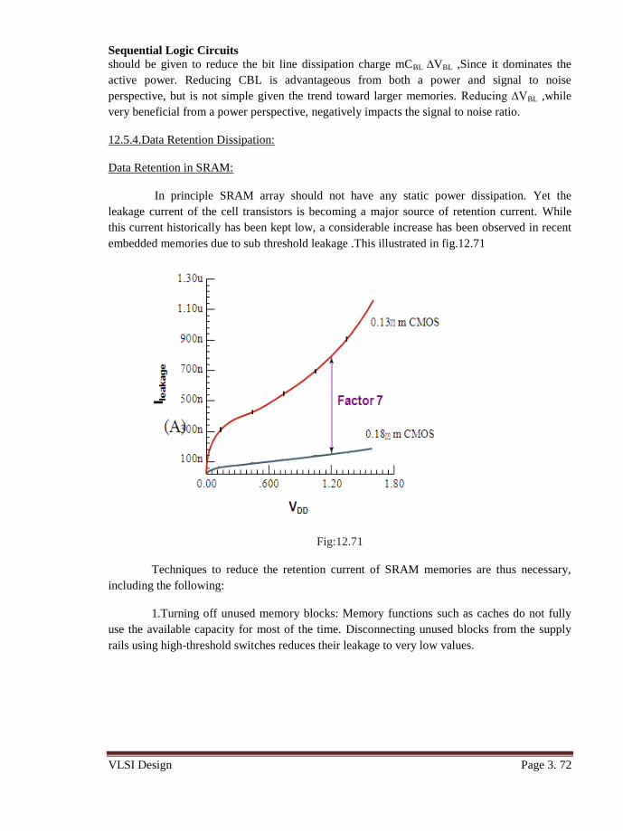
Sequential Logic Circuits
VLSI Design Page 3. 72
should be given to reduce the bit line dissipation charge mCBL ∆VBL ,Since it dominates the
active power. Reducing CBL is advantageous from both a power and signal to noise
perspective, but is not simple given the trend toward larger memories. Reducing ∆VBL ,while
very beneficial from a power perspective, negatively impacts the signal to noise ratio.
12.5.4.Data Retention Dissipation:
Data Retention in SRAM:
In principle SRAM array should not have any static power dissipation. Yet the
leakage current of the cell transistors is becoming a major source of retention current. While
this current historically has been kept low, a considerable increase has been observed in recent
embedded memories due to sub threshold leakage .This illustrated in fig.12.71
Fig:12.71
Techniques to reduce the retention current of SRAM memories are thus necessary,
including the following:
1.Turning off unused memory blocks: Memory functions such as caches do not fully
use the available capacity for most of the time. Disconnecting unused blocks from the supply
rails using high-threshold switches reduces their leakage to very low values.
www.AllAbtEngg.com
AllAbtEngg Android Application for Anna University, Polytechnic & School
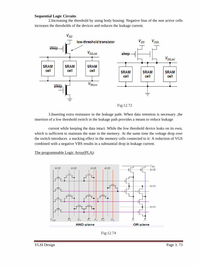
Sequential Logic Circuits
VLSI Design Page 3. 73
2.Increasing the threshold by using body biasing: Negative bias of the non active cells
increases the thresholds of the devices and reduces the leakage current.
Fig:12.72
3.Inserting extra resistance in the leakage path: When data retention is necessary ,the
insertion of a low threshold switch in the leakage path provides a means to reduce leakage
current while keeping the data intact. While the low threshold device leaks on its own,
which is sufficient to maintain the state in the memory. At the same time the voltage drop over
the switch introduces a stacking effect in the memory cells connected to it: A reduction of VGS
combined with a negative VBS results in a substantial drop in leakage current.
The programmable Logic Array(PLA):
Fig:12.74
www.AllAbtEngg.com
AllAbtEngg Android Application for Anna University, Polytechnic & School
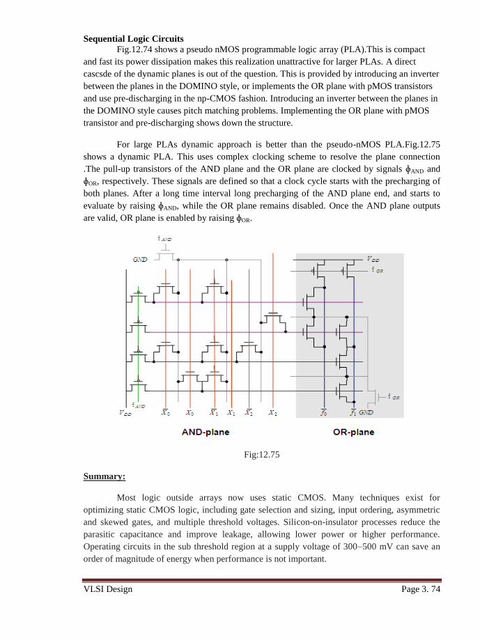
Sequential Logic Circuits
VLSI Design Page 3. 74
Fig.12.74 shows a pseudo nMOS programmable logic array (PLA).This is compact
and fast its power dissipation makes this realization unattractive for larger PLAs. A direct
cascsde of the dynamic planes is out of the question. This is provided by introducing an inverter
between the planes in the DOMINO style, or implements the OR plane with pMOS transistors
and use pre-discharging in the np-CMOS fashion. Introducing an inverter between the planes in
the DOMINO style causes pitch matching problems. Implementing the OR plane with pMOS
transistor and pre-discharging shows down the structure.
For large PLAs dynamic approach is better than the pseudo-nMOS PLA.Fig.12.75
shows a dynamic PLA. This uses complex clocking scheme to resolve the plane connection
.The pull-up transistors of the AND plane and the OR plane are clocked by signals ɸAND and
ɸOR, respectively. These signals are defined so that a clock cycle starts with the precharging of
both planes. After a long time interval long precharging of the AND plane end, and starts to
evaluate by raising ɸAND, while the OR plane remains disabled. Once the AND plane outputs
are valid, OR plane is enabled by raising ɸOR.
Fig:12.75
Summary:
Most logic outside arrays now uses static CMOS. Many techniques exist for
optimizing static CMOS logic, including gate selection and sizing, input ordering, asymmetric
and skewed gates, and multiple threshold voltages. Silicon-on-insulator processes reduce the
parasitic capacitance and improve leakage, allowing lower power or higher performance.
Operating circuits in the sub threshold region at a supply voltage of 300–500 mV can save an
order of magnitude of energy when performance is not important.
www.AllAbtEngg.com
AllAbtEngg Android Application for Anna University, Polytechnic & School
Sequential Logic Circuits
VLSI Design Page 3. 75
Three of the historically important alternatives to complementary CMOS are domino,
pseudo-nMOS, and pass transistor logic. Each attempts to reduce the input capacitance by
performing logic mostly through nMOS transistors. Power, robustness, and productivity issues
have largely eliminated these techniques from data paths and random logic, though niche
applications still exist, especially in arrays.
www.AllAbtEngg.com
AllAbtEngg Android Application for Anna University, Polytechnic & School