
CHAPTER 5 THREE TRANSISTORS (3T) BASED...
38
111 CHAPTER 5 THREE TRANSISTORS (3T) BASED LOGIC GATES 5.1 INTRODUCTION This Chapter presents an area and energy efficient OR, AND, Universal NAND and NOR gates. The proposed robust three transistors (3T) based gates are just as effective for dynamic power control in CMOS VLSI circuits for System on Chip (SoC) applications. The 3T based logic gates intuitively momentous and lead to better performance measures in terms of dynamic power, reduced area and high speed while maintaining comparable performance than the other available logic gate structures. The importance of universal gates is described which is followed by CMOS inverter and Pass Transistor Logic (PTL) that are used to build the 3T based logic gates. This chapter will give detailed operation of 3T based logic gates with transistor sizing and existing logic structures of gates to compare with 3T based logic gates. Finally, a D-latch is implemented with the proposed 3T NAND gate. 5.2 SIGNIFICANCE OF UNIVERSAL GATES In order to realize ultra low power SOC applications, circuits should be operated with low power dissipating gates. In reality, digital control systems have been designed approximately with either NAND or NOR gates, all the essential logic functions being derived from collections of interconnected NANDs or NORs. Low power and high reliability needs along with cost/performance advantages make NAND flash memory the ideal data storage solution for portable electronics.
-
Upload
trinhxuyen -
Category
Documents
-
view
295 -
download
0
Transcript of CHAPTER 5 THREE TRANSISTORS (3T) BASED...
111
CHAPTER 5
THREE TRANSISTORS (3T) BASED LOGIC GATES
5.1 INTRODUCTION
This Chapter presents an area and energy efficient OR, AND,
Universal NAND and NOR gates. The proposed robust three transistors (3T)
based gates are just as effective for dynamic power control in CMOS VLSI
circuits for System on Chip (SoC) applications. The 3T based logic gates
intuitively momentous and lead to better performance measures in terms of
dynamic power, reduced area and high speed while maintaining comparable
performance than the other available logic gate structures. The importance of
universal gates is described which is followed by CMOS inverter and Pass
Transistor Logic (PTL) that are used to build the 3T based logic gates. This
chapter will give detailed operation of 3T based logic gates with transistor
sizing and existing logic structures of gates to compare with 3T based logic
gates. Finally, a D-latch is implemented with the proposed 3T NAND gate.
5.2 SIGNIFICANCE OF UNIVERSAL GATES
In order to realize ultra low power SOC applications, circuits
should be operated with low power dissipating gates. In reality, digital control
systems have been designed approximately with either NAND or NOR gates,
all the essential logic functions being derived from collections of
interconnected NANDs or NORs. Low power and high reliability needs along
with cost/performance advantages make NAND flash memory the ideal data
storage solution for portable electronics.

112
The significance of a universal gate is that programmable chips can
be made up of only one kind of gate, either NAND or NOR gate making
manufacturing process simple and reducing the numbers of different
processors required to make a computer. The benefit of utilizing a
combination of low-power components in conjunction with low-power design
methodologies is more important now than ever before. Low power
requirements continue to grow extensively as components become battery-
powered, smaller and require more functionality.
describes a long-term trend in the history of
computing hardware and has actually been somewhat faster than Moore
law. Jonathan Koomey
load, the amount of battery you need will fall by a factor of two every year
Koomey Jonathan 2011). Designers are progressively more
turning to embedded NAND solutions for dynamic, on-board storage. To
support the ever-changing needs of current and emerging applications, the
authors have developed the most appropriate NAND solution for these
applications.
5.3 NAND PREFERRED THAN NOR
The PMOS devices in series lead to very poor rise time
performances as poor output node charge to VDD in conventional CMOS NOR
gate. Meanwhile, the CMOS NMOS device in parallel provides a very
efficient path for discharge to ground, leading a short fall time. Due to this
non-symmetrical behaviour NAND gate based designs are preferred because
of the PMOS in parallel which naturally compensate the poor hole mobility of
their channel, producing symmetrical switching characteristics than NOR
gate.

113
Due to importance of NAND gate, the 3T based NAND gate is
simulated and analysed in 90nm, 45nm and 22nm process technologies. The
3T NAND gate has been compared with other existing NAND gate structures
at 90nm process technology. A D-latch is designed using 3T NAND gate and
compared with other existing D-Latch structures. Also C17 benchmark circuit
is used for 3T NAND gate evaluation.
5.4 REVIEW OF CMOS INVERTER AND PTL
5.4.1 CMOS Inverter
CMOS inverters are some of the most largely used and adaptable
MOSFET inverters in chip designing. They operate with minimal power loss
and at relatively high speed. Furthermore, the CMOS inverter has good logic
buffer characteristics in that. Its noise margins are large in both low and high
states.
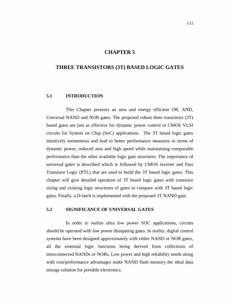
A CMOS inverter shown in Figure 5.1 contains a PMOS and a
NMOS devices connected at the drain and gate terminals, a supply voltage
VDD at the PMOS source terminal, and a ground connected at the NMOS
source terminal, were INPUT is connected to the gate terminals and OUTPUT
is connected to the drain terminals. As the input to the inverter varies between
logic 0 and logic 1, the state of the NMOS and PMOS varies accordingly to
make output as logic 1 and logic 0 respectively.
114
Figure 5.1 CMOS Inverter
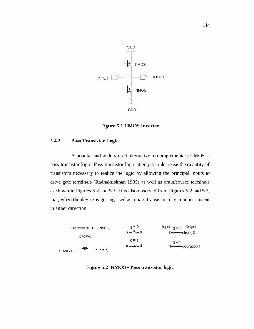
5.4.2 Pass Transistor Logic
A popular and widely used alternative to complementary CMOS is
pass-transistor logic. Pass-transistor logic attempts to decrease the quantity of
transistors necessary to realize the logic by allowing the principal inputs to
drive gate terminals (Radhakrishnan 1985) as well as drain/source terminals
as shown in Figures 5.2 and 5.3. It is also observed from Figures 5.2 and 5.3,
that, when the device is getting used as a pass-transistor may conduct current
in either direction.
Figure 5.2 NMOS - Pass transistor logic

115
Figure 5.3 PMOS - Pass transistor logic
The NMOS transistors pass a strong logic 0 but a weak logic
1(threshold voltage drop. High =VDD -Vthn) and PMOS transistors pass a
strong logic 1 but a weak logic 0(threshold voltage drop. Low = Vthp). Thus,
NMOS switches are best for pull-down network and the PMOS switches are
best for pull-up network. Keeping these in view, the study adopted a
quasi-experimental research method.
5.5 DESIGN OF 3T LOGIC GATES
The 3T OR and AND gates design is based on PMOS and NMOS
Pass Transistor Logic (PTL). The 3T NAND and NOR gates design is based
on CMOS inverter and PTL. Output voltage degradation occurs across the
PMOS and NMOS pass transistors due to threshold voltage drop while
passing the logic zero or logic one respectively in relation to the input. The
voltage degradation caused by threshold drop can be considerably minimized
by escalating the W/L ratio of the pass transistor. Equation (5.1) relates the
threshold voltage of a MOS transistor to its channel length and width.
+ g - 1 -
( v w (5.1)

116
where tOX is the thickness of the oxide layer, is the zero bias threshold
voltage, g is bulk threshold coefficient, is 2 , where is the Fermi
1, v and w are process dependent parameters. From
Equation (5.1), it is obvious that by increasing the width W of a transistor,
keeping the length constant it is possible to reduce the voltage degradation
due to the threshold voltage.
5.5.1 Three Transistors based OR Gate
The 3T OR gate is shown in Figure 5.4. Typical values of
PMOS PMOS M2, and
NMOS M3 have been taken. The length for all the transistors
for 22nm process
technology.
Figure 5.4 Three transistors based OR gate
When input A = input B= 0, the two PMOS M1 and M2 are
ON and NMOS M3 is OFF. The transistors M1 and M2
functions as a pass transistor (Transistor M1 is more stronger
than other transistor M2 and passes B ) giving an output logic
zero.
117
When input A=0 and input B=1, transistor M1 is ON and
transistors M2 and M3 are OFF. Transistor M1 passes the
input B=1 to the output.
When input A=1 and input B=0, transistor M1 is OFF and
transistors M2 and M3 are ON passing input A to give an
output logic 1.
When input A=1 and input B=1, the transistors M1 and M2
are OFF and transistor M3 is ON passing VDD, a logic 1 at
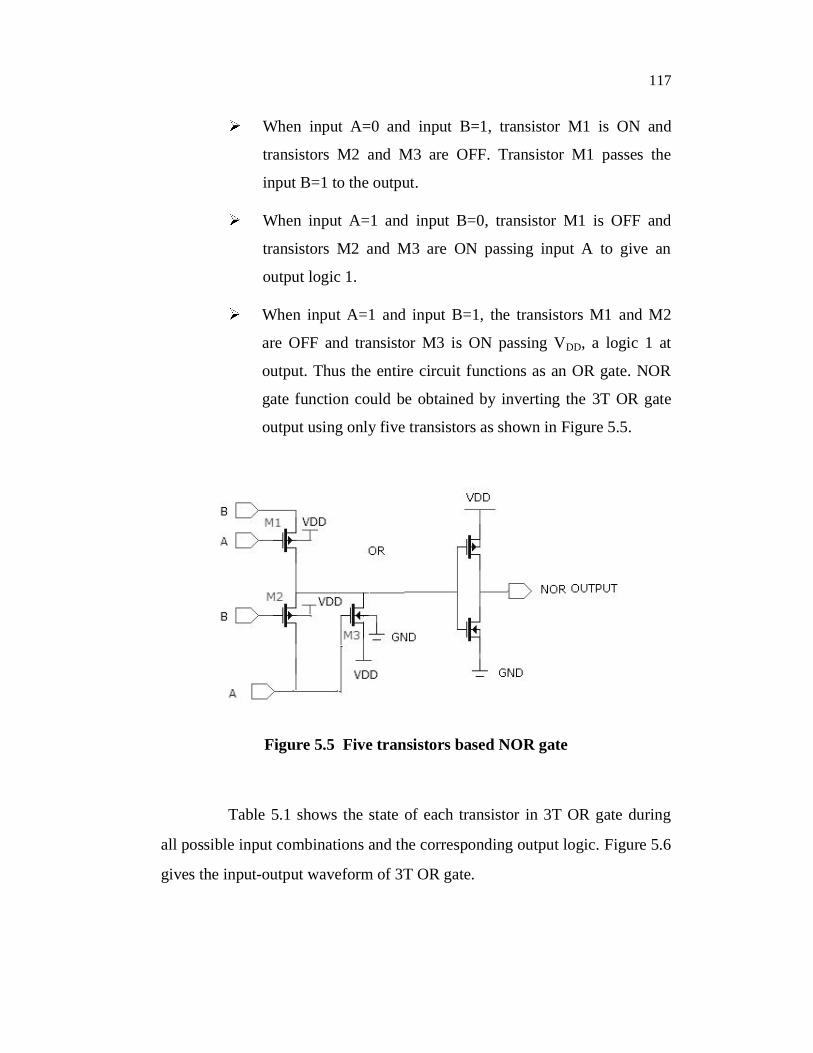
output. Thus the entire circuit functions as an OR gate. NOR
gate function could be obtained by inverting the 3T OR gate
output using only five transistors as shown in Figure 5.5.
Figure 5.5 Five transistors based NOR gate
Table 5.1 shows the state of each transistor in 3T OR gate during
all possible input combinations and the corresponding output logic. Figure 5.6
gives the input-output waveform of 3T OR gate.

118
Table 5.1 State table of 3T OR gate
Inputs Transistor State OR Output
A B M1 M2 M3 0 0 On On Off 0/ B
0 1 On Off Off 1/B
1 0 Off On On 1/ A 1 1 Off Off On 1/ VDD
Figure 5.6 Input/output waveform of 3T OR gate @ 22nm with VDD=0.2V
5.5.2 Three Transistors based AND Gate
The 3T AND gate is shown in Figure 5.7. Typical values of

119
Figure 5.7 Three transistors based AND gate
When input A = input B= 0, the two NMOS M1 and M2 are
OFF and PMOS M3 is ON. The transistors M3 connects the
output line to ground giving an output logic zero.
When input A=0 and input B=1, transistor M1 is ON and
transistors M2 and M3 are OFF. Transistor M1 passes the
input A=0 to the output.
When input A=1 and input B=0, transistor M1 is OFF and
transistors M2 and M3 are ON passing input B to give an
output logic 0.
When input A=1 and input B=1, the transistors M1 and M2
are ON and transistor M3 is OFF. This condition passes input
A giving a logic 1 at output (Transistor M1 is more stronger
than other transistor M2 and passes A). The NAND gate
function could be obtained by inverting the 3T AND gate
output as shown in Figure 5.8 using only five transistors.
120
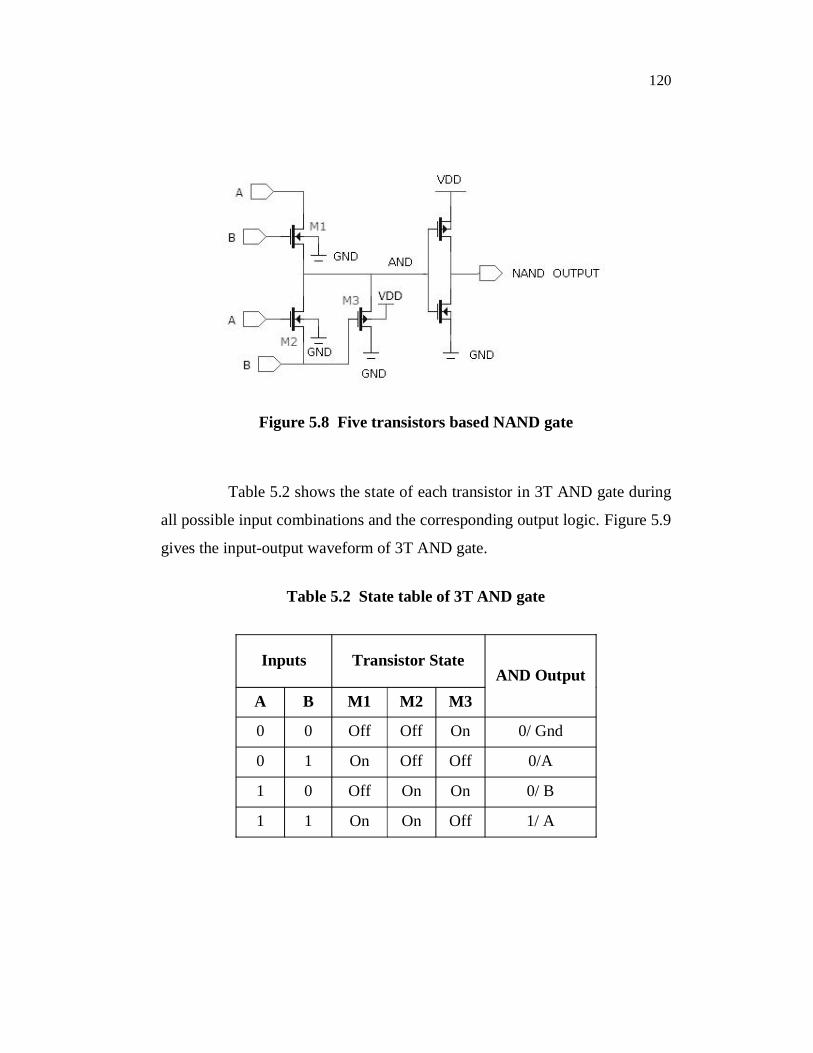
Figure 5.8 Five transistors based NAND gate
Table 5.2 shows the state of each transistor in 3T AND gate during
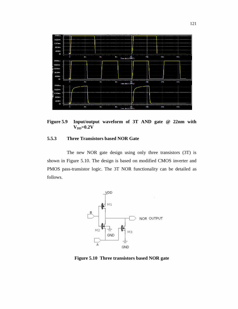
all possible input combinations and the corresponding output logic. Figure 5.9
gives the input-output waveform of 3T AND gate.
Table 5.2 State table of 3T AND gate
Inputs Transistor State AND Output
A B M1 M2 M3
0 0 Off Off On 0/ Gnd
0 1 On Off Off 0/A
1 0 Off On On 0/ B
1 1 On On Off 1/ A
121
Figure 5.9 Input/output waveform of 3T AND gate @ 22nm with VDD=0.2V
5.5.3 Three Transistors based NOR Gate
The new NOR gate design using only three transistors (3T) is
shown in Figure 5.10. The design is based on modified CMOS inverter and
PMOS pass-transistor logic. The 3T NOR functionality can be detailed as
follows.
Figure 5.10 Three transistors based NOR gate

122
The PMOS M1 and NMOS M2 on the left form a modified
CMOS inverter structure. The NMOS M3 on the right acts as
a pass transistor.
When A=0, M3 is OFF and the modified inverter on the left
(M1 and M2) functions as a normal CMOS inverter.
Therefore, the output is the complement of input B.
When A=1 and B=0 , M2 is OFF, M1 and M3 are ON which
pull up the output node while M3 tends to pull down the
output node.
Similarly when A=1 and B=1, M1 is OFF, M2 and M3 are ON
M2 tends to
pull up the output node while M3 tends to pull down the
output node.
For A=1 and
is possible to obtain exact output logic levels with the
proposed circuit, if the channel width of M3 is made 6 times
that of M2 or 3 times that of M1.
(i.e) WM3 = 6 x WM2 = 3 x WM1
Thus M3 becomes much stronger than M1 and M2, giving a strong
of the channel for all transistors was
M1,WM1 M2
width of M3, WM3
123
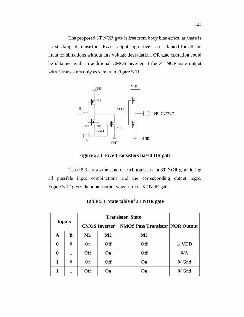
The proposed 3T NOR gate is free from body bias effect, as there is
no stacking of transistors. Exact output logic levels are attained for all the
input combinations without any voltage degradation. OR gate operation could
be obtained with an additional CMOS inverter at the 3T NOR gate output
with 5 transistors only as shown in Figure 5.11.
Figure 5.11 Five Transistors based OR gate
Table 5.3 shows the state of each transistor in 3T NOR gate during
all possible input combinations and the corresponding output logic.
Figure 5.12 gives the input-output waveform of 3T NOR gate.
Table 5.3 State table of 3T NOR gate
Inputs Transistor State
NOR Output CMOS Inverter NMOS Pass Transistor
A B M1 M2 M3
0 0 On Off Off 1/ VDD
0 1 Off On Off 0/A
1 0 On Off On 0/ Gnd
1 1 Off On On 0/ Gnd
124
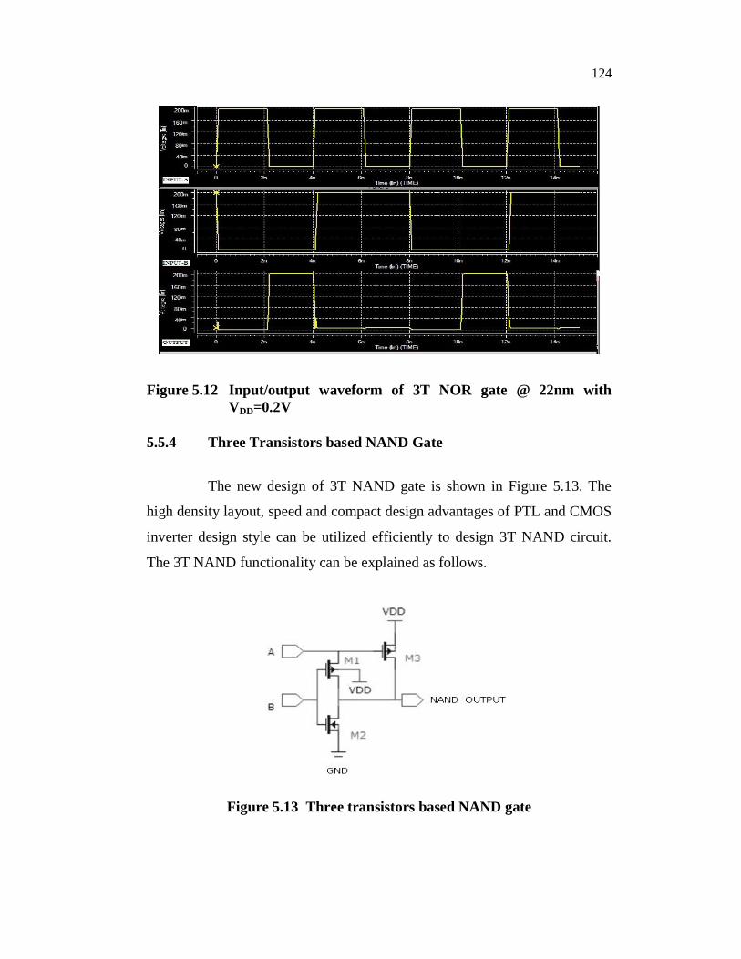
Figure 5.12 Input/output waveform of 3T NOR gate @ 22nm with VDD=0.2V
5.5.4 Three Transistors based NAND Gate
The new design of 3T NAND gate is shown in Figure 5.13. The
high density layout, speed and compact design advantages of PTL and CMOS
inverter design style can be utilized efficiently to design 3T NAND circuit.
The 3T NAND functionality can be explained as follows.
Figure 5.13 Three transistors based NAND gate

125
The PMOS M1 and NMOS M2 on the left form a modified
CMOS inverter structure. The PMOS M3 on the right acts as a
pass transistor.
When A=1, M3 is OFF and the modified inverter on the left
(M1 and M2) functions as a normal CMOS inverter.
Therefore, the output is the complement of input B.
When A=0 and B=0 , M2 is OFF, M1 and M3 are ON which
pull down the output node while M3 tends to pull up the
output node. Similarly when A=0 and B=1, M1 is OFF, M2
because M2 tends to pull down the output node while M3
tends to pull up the output node.
For A=0 and t is required. It
is possible to obtain exact output logic levels with the
proposed circuit, if the channel width of M3 is made 6 times
that of M2 or 3 times that of M1.
(i.e) WM3 = 6 x WM2 = 3 x WM1
Thus M3 becomes much stronger than M1 and M2, giving a strong
er understandable from
Table 5.4.
The proposed 3T NAND gate is exempt from body bias effect, as
there is no stacking of transistors. Exact output logic levels are attained for all
the input combinations without any voltage degradation. An AND gate
operation could be obtained with an additional CMOS inverter at the 3T
NAND gate output with 5 transistors totally as shown in Figure 5.14.
Table 5.4 shows the state of each transistor in 3T NAND gate for various
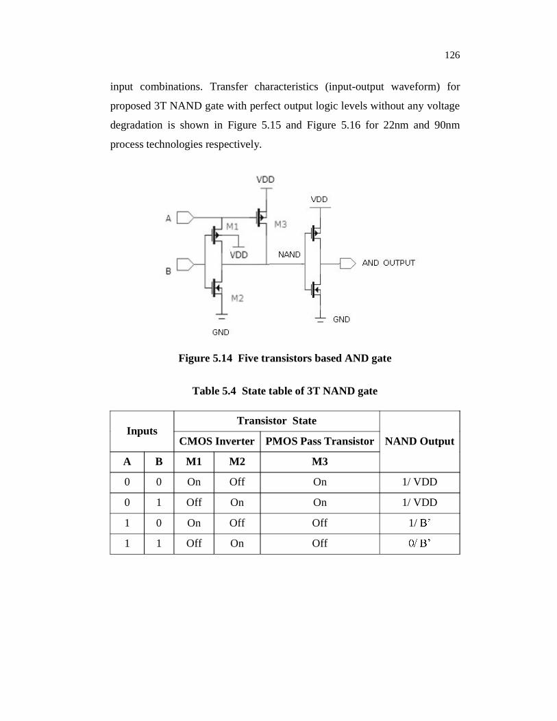
126
input combinations. Transfer characteristics (input-output waveform) for
proposed 3T NAND gate with perfect output logic levels without any voltage
degradation is shown in Figure 5.15 and Figure 5.16 for 22nm and 90nm
process technologies respectively.
Figure 5.14 Five transistors based AND gate
Table 5.4 State table of 3T NAND gate
Inputs Transistor State
NAND Output CMOS Inverter PMOS Pass Transistor
A B M1 M2 M3
0 0 On Off On 1/ VDD
0 1 Off On On 1/ VDD
1 0 On Off Off 1/
1 1 Off On Off

127
Figure 5.15 Transfer characteristics of 3T NAND gate at 22nm with VDD=0.2V
Figure 5.16 Transfer characteristics of 3T NAND gate at 90nm with VDD =1V

128
5.6 EXISTING LOGIC STRUCTURES FOR COMPARISON
Logic gates of different logic structures reported in literature such
as CMOS Logic, Double Pass Transistor Logic, Complementary Pass
transistor Logic and Dual Value Logic have been considered for comparison
with 3T logic gates for performance evaluation.
5.6.1 Complementary CMOS Logic Style
Logic gates in conventional or complementary CMOS (also simply
referred to as CMOS in the sequel) are built from an NMOS pull-down and a
dual PMOS pull-up logic network. In addition, pass-gates or transmission
gates (i.e., the combination of an NMOS and a PMOS pass-transistor) are
often used for implementing multiplexers, XOR-gates, and flip-flops
efficiently. Any logic function can be realized by NMOS pull-down and
PMOS pullup networks connected between the gate output and the power
lines. Figure 5.17 shows logic gates in CMOS structure.
(a) (b) (c) (d)
Figure 5.17 Gates in CMOS logic (a) OR (b)AND (c)NOR and (d)NAND
129
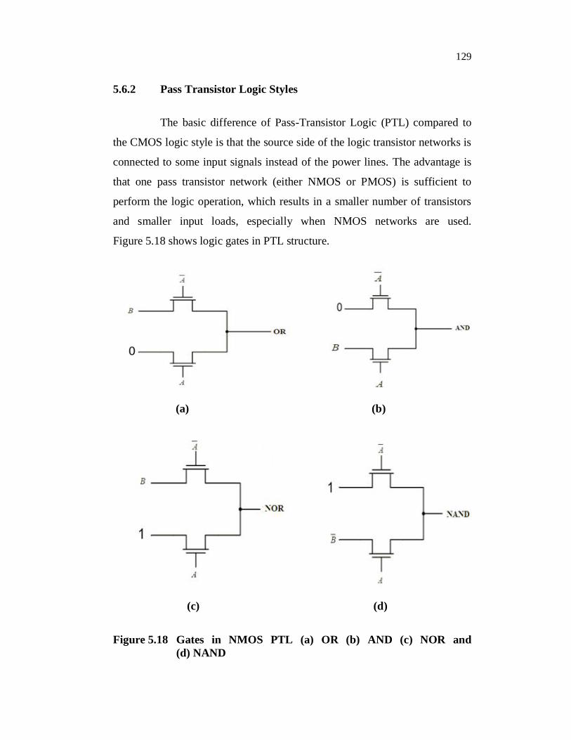
5.6.2 Pass Transistor Logic Styles
The basic difference of Pass-Transistor Logic (PTL) compared to
the CMOS logic style is that the source side of the logic transistor networks is
connected to some input signals instead of the power lines. The advantage is
that one pass transistor network (either NMOS or PMOS) is sufficient to
perform the logic operation, which results in a smaller number of transistors
and smaller input loads, especially when NMOS networks are used.
Figure 5.18 shows logic gates in PTL structure.
(a) (b)
(c) (d)
Figure 5.18 Gates in NMOS PTL (a) OR (b) AND (c) NOR and (d) NAND

130
5.6.3 Complementary Pass-Transistor Logic
Complementary Pass-Transistor Logic (CPL) consists of
complementary inputs/outputs, a NMOS pass-transistor network, and CMOS
output inverters. The circuit function is implemented as a tree consisting of
pull-down and pull-up branches. Since the threshold voltage drop of NMOS
-transistor output nodes, the output
signals are restored by CMOS inverters. CPL has traditionally been applied to
the arithmetic building blocks and has been shown to result in high speed
operation due to its low input capacitance and reduced transistor count. All
two-input functions (e.g.AND, OR,XOR, XNOR, NAND AND NOR) can be
implemented by this basic gate structure, which is relatively expensive for
simple monotonic gates such as NAND and NOR. Figure 5.19 shows logic
gates in CPL structure.
(a) (b)
Figure 5.19 Gates in CPL (a) AND-NAND (b)OR-NOR

131
5.6.4 Double Pass-Transistor Logic
To avoid problems of reduced noise margins in CPL, twin PMOS
transistor branches are added to N-tree in DPL. This addition results in
increased input capacitances. However its symmetrical arrangement and
double-transmission characteristics compensate for the speed degradation
arising from increased loading. The full swing operation improves circuit
performance at reduced supply voltage with limited threshold voltage scaling.
Figure 5.20 shows logic gates in DPL structure.
(a) (b)
(c) (d)
Figure 5.20 Gates in DPL (a)OR (b)AND (c)NOR and (d)NAND

132
5.6.5 Dual Value Logic
The main drawback of Dual Value Logic (DPL) is its redundancy,
i.e.) it requires more transistors than actually needed for the realization of a
function. To overcome the problem of redundancy, a new logic family, DVL,
is derived from DPL. It preserves the full swing operation of DPL with
reduced transistor count. Figure 5.21 shows logic gates in DVL structure.
(a) (b)
(c) (d)
Figure 5.21 Gates in DVL (a)OR (b)AND (c)NOR and (d)NAND

133
5.7 SIMULATION RESULTS
5.7.1 Evaluation of 3T Logic Gates
In order to compare the results of proposed 3T based logic gates
with existing logic gate structures, a set of experiments was carried
out. Schematics were designed for all circuits using Custom Designer in
schematics are used to simulate and test performance.
The original netlists are modified according to the process
technology targeted using Berkeley Predictive Technology Model (BPTM)
22nm process. The modified netlists are simulated using Synopsys HSPICE
for power and delay estimations. The worst case power and delay
measurements are made in all the cases with the operating temperature as
27°C. The performance of the circuit is evaluated based on their power
dissipation and delay.
The transfer characteristics of proposed 3T logic gates using
HSPICE gave exact output logic levels without any voltage degradation.
Logic gates of different logic structures reported in literature such as CMOS
Logic, Double Pass Transistor Logic, Complementary Pass transistor Logic
and Dual Value Logic have been simulated and comparisons have been
presented in Table 5.5.
For all logics except 3T logic gates, the transistor sizes are taken as
width WP PMOS and Wn NMOS with constant length
All devices used are of standard threshold voltage
(Vth). Figure 5.22 show that the proposed logic gates have the minimal
number of transistors than the other logic gates.

134
Figure 5.22 Number of transistors for various logics
From the results in Table 5.5, the following can be inferred :
The dynamic power dissipation and area increases with the
increase in number of switching transistors.
Column 10 indicates that there is a lower power dissipation
(dynamic and leakage) for a 3 transistor based logic gates
compared to other logic gate structures.
With a focus on delay, from column 11, the optimum delay for
3 transistor based logic gates obtained.
Column 12 shows that 3T logic gates provide an average of
87.5% power savings compared with CMOS base case.

135
Table 5.5 Power dissipation (W) and delay (ps) profiles for the logic gate circuits in 22nm process technology
Logic
Gate @ VDD= 0.2V
CMOS logic Double Pass Transistor Logic
(DPL)
Complementary Pass Transistor
Logic (CPL)
Dual Value Logic (DVL)
Proposed 3T based Power Savings
compared to CMOS Power Delay Power Delay Power Delay Power Delay Power Delay
OR 3.6147 E-12 63.8 6.3240 E-12 55.8 4.1832 E-12 57.0 5.2846 E-12 67.2 1.6182 E-12 35.7 123X
AND 3.9532 E-12 51.9 5.9632 E-12 53.3 4.6108 E-12 45.8 5.8142 E-12 54.2 1.4928 E-12 32.5 164X
NAND 2.4743 E-12 47.1 5.5184 E-12 49.5 5.8200 E-12 51.3 3.6920 E-12 51.6 1.8661 E-12 38.2 33X
NOR 2.7644 E-12 54.8 5.7154 E-12 53.2 6.0181 E-12 53.8 3.9153 E-12 59.8 1.9121 E-12 39.2 45X
136
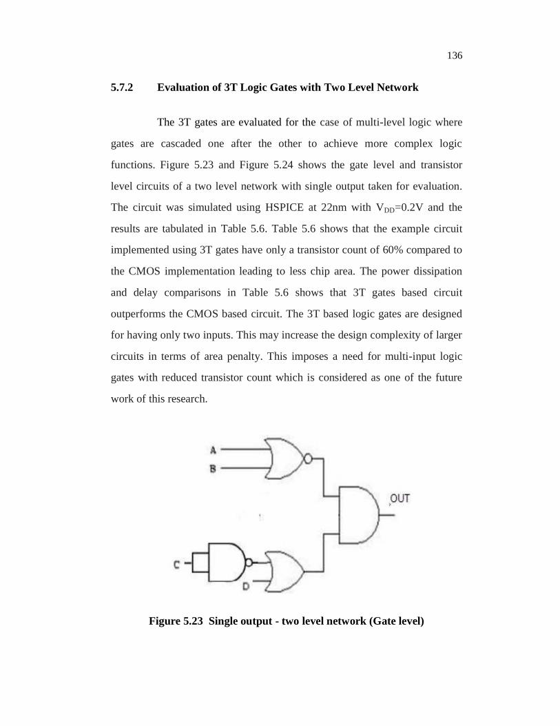
5.7.2 Evaluation of 3T Logic Gates with Two Level Network
The 3T gates are evaluated for the case of multi-level logic where
gates are cascaded one after the other to achieve more complex logic
functions. Figure 5.23 and Figure 5.24 shows the gate level and transistor
level circuits of a two level network with single output taken for evaluation.
The circuit was simulated using HSPICE at 22nm with VDD=0.2V and the
results are tabulated in Table 5.6. Table 5.6 shows that the example circuit
implemented using 3T gates have only a transistor count of 60% compared to
the CMOS implementation leading to less chip area. The power dissipation
and delay comparisons in Table 5.6 shows that 3T gates based circuit
outperforms the CMOS based circuit. The 3T based logic gates are designed
for having only two inputs. This may increase the design complexity of larger
circuits in terms of area penalty. This imposes a need for multi-input logic
gates with reduced transistor count which is considered as one of the future
work of this research.
Figure 5.23 Single output - two level network (Gate level)

137
Figure 5.24 Single output - two level network (Transistor level)
Table 5.6 Simulation results for single output - two level network
Circuit CMOS Based Proposed 3T Based
Dynamic Power (W) 21.5219 E-12 15.2663 E-12
Delay (ps) 74.5 59.1
No. of transistors 20 12
5.7.3 Additional Experiments on 3T NAND Gate
Additional experiments were carried out on 3T NAND gate due to
its significance in low power applications. The Performance of the 3T NAND
gate is evaluated by employing standard Berkeley Predictive Technology
Model (BPTM) 22nm, 45nm and 90nm process technologies. The experiment
and simulation results show that, proposed 3T NAND gate effectively

138
outperforms the basic CMOS NAND gate with excellent driving capability
and signal integrity with exact output logic levels. All devices used are of
standard threshold voltage and the operating temperature taken is 27°C. The
3T NAND gate ensures optimum performance for frequency range between
50MHz to 0.3GHz. All the results were simulated and analyzed in the range
of 125 MHz to 0.25GHz.
Figure 5.25 gives the layout of 3T NAND gate. Table 5.7 shows the
simulation results of 3T & 4T NAND gates compared at 90nm, 45nm and
22nm process technology (Zhao and Cao, 2006). Dynamic power dissipation
is estimated by applying all four possible input vectors (00, 01, 10 and 11)
arbitrarily. Table 5.8 gives the simulation results of 3T NAND at 22nm
process for various supply voltages (0.2 V, 0.45V, 0.6V & 0.75V).
Transistor sizing details are given as:
WM1 M2
channel width of M3, WM3
Fo
WM1 M2
channel width of M3, WM3
he length of the channel for all
WM1 M2
channel width of M3, WM3

139
Figure 5.25 3T NAND layout
From Table 5.7, the following can be inferred:
Considering the power dissipation, 3T NAND gate shows less
dynamic power dissipation compared to conventional CMOS
NAND gate. The reduction in dynamic power dissipation
comes from the fact of reduced internal capacitances as
transistors count is less, which results in less glitches at the
outputs.
With regards of the speed, it can be seen the benefit of the
pass transistor logic structure introduced here, exhibiting the
smallest propagation delay than CMOS NAND gate.
The Power Delay Product (PDP) column confirms the energy-
efficiency for the 3T NAND gate built using the new logic
structure. They present the lowest PDP metric, due to the
combined reduction of power consumption and propagation
delay.

140
Table 5.7 Simulation results of NAND gate for various process technologies
Parameters
90nm@VDD=1.2V 45nm@VDD=0.5V 22nm @ VDD=0.2V
3T NAND 4T CMOS
NAND 3T NAND
4T CMOS NAND
3T NAND 4T CMOS
NAND
Dynamic power (W)
8.4200 E-09 10.2812 E-09 4.9058 E-11 6.1356 E-11 1.8661 E-12 2.4743 E-12
Delay(ps) 54.8 75.2 43.6 59.4 38.2 47.1
PDPdynamic(J) 461.4 E-21 773.1 E-21 213.8 E-23 364.4 E-23 71.2 E-24 116.5 E-24
From Table 5.8, the following can be inferred:
In addition, separate set of simulations are carried out to
determine the maximum power supply voltage that 3T NAND
gate can tolerate at 0.022µm (22nm) process technology while
maintaining its correct functionality. As shown in column 1,
supply voltage, the proposed NAND can operate properly with
0.2 to 0.8 V supply voltage.
With increase in supply voltage, the dynamic power increases
and the delay improves.
The average power column for different input vectors shows
the fact that subthreshold leakage is dependent on input
vectors.
On regards of the implementation area, it can be seen that the
proposed NAND gate require the smallest area due to less
transistor count, which can also be considered as one of the
factors for presenting lower delay and power consumption.
It is a good candidate for battery-operated applications where
low dissipation modules with standby modes are required.

141
Table 5.8 Simulation results of 3T NAND gate @ 0.022 22nm) for various supply voltages (supply voltage in V, power in W and delay in ps)
Supply Voltage
Dynamic Power
Delay Average Power for Various Input Vectors
00 01 10 11
0.2 1.8661 E-12 38.2 3.0021 E-13 5.8750 E-13 1.7239 E-13 1.4215 E-14
0.45 5.8167 E-12 37.4 6.7812 E-13 9.0081 E-13 5.0414 E-13 4.6900 E-14
0.6 10.6535 E-12 37.0 9.3406 E-13 11.1775 E-13 8.6580 E-13 7.8640 E-14
0.75 16.3971 E-12 36.6 11.3810 E-13 12.3462 E-13 9.4174 E-13 10.8979 E-14
Figure 5.26 gives the percentage of power savings of 3T NAND
gate showing an improvement of more than 22% of less power consumption
over conventional CMOS NAND Gate (4T) as the process technology
diminishes.
Figure 5.26 Power savings of 3T NAND gate

142
From the results in Table 5.9, the following can be inferred :
The dynamic power dissipation, leakage power dissipation
and area increases with the increase in number of switching
transistors.
The rows 3 and 7 indicate that there is a lower power
dissipation (dynamic and leakage) for a 3 transistor based
NAND gate compared to other NAND gate circuits.
With a focus on delay, from rows 4 and 5 the optimum delay
and power delay product for a 3 transistor based NAND gate
can be obtained.
The implementation area obtained from the layouts, it can be
seen that 3 transistor based NAND gate require smaller area
as compared to other circuits , as shown in row 6.
Table 5.9 Simulation results for the NAND gate circuits in 90nm process technology
NAND Circuit @ VDD=1 V
CMOS Logic
DPL CPL PTL DVL Proposed 3T NAND
No. of Transistors 4 8 6 6 5 3
Dynamic Power Dissipation ( E -09 W)
7.7644 8.4314 8.7501 7.5278 7.0761 6.4626
Delay (ns) 0.0785 0.0765 0.0761 0.0961 0.0725 0.0575
Power Delay Product (E-15 J) (dynamic)
0.6095 0.6450 0.6658 0.7234 0.5130 0.3715
Area (µm2) 36.29 66.8 67.3 51.8 43.9 28.86
Leakage Power (E-012 W) (stand by)
0.8 1.4 1.7 1.02 0.89 0.5

143
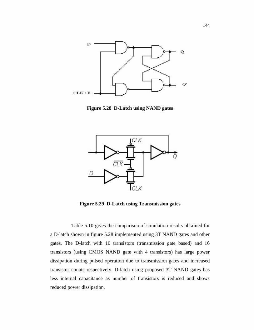
5.7.4 D-Latch Implementation
A D-latch has one input, labeled D, one enable or clock input, and
one output Q as shown in the symbol of a D-Latch in Figure 5.27. The logical
state of the D input is transferred to the output whenever the clock /enable
(CLK/E) input is HIGH. The Q output will follow any changes in the logical
state of the D input as long as the clock input remains HIGH.
When the clock input goes LOW the logical state of the D input at
that moment will be retained at the Q output no matter what changes occur at
the D input. When the clock input goes HIGH again the Q output will once
again follow any changes in the logical state of the D input. A D latch is
therefore said to be transparent when the clock is HIGH. Figure 5.28 and
Figure 5.29 gives the NAND gate and transmission gate based
implementations respectively.
Figure 5.27 D- Latch
144
Figure 5.28 D-Latch using NAND gates
Figure 5.29 D-Latch using Transmission gates
Table 5.10 gives the comparison of simulation results obtained for
a D-latch shown in figure 5.28 implemented using 3T NAND gates and other
gates. The D-latch with 10 transistors (transmission gate based) and 16
transistors (using CMOS NAND gate with 4 transistors) has large power
dissipation during pulsed operation due to transmission gates and increased
transistor counts respectively. D-latch using proposed 3T NAND gates has
less internal capacitance as number of transistors is reduced and shows
reduced power dissipation.

145
Table 5.10 Simulation results for D-latch @ 90nm process technology and VDD=1V
D latch Circuit No. of
Transistors
Dynamic Power
Dissipation (W)
Delay (ns)
PDPdynamic (J)
Using 2 transmission gate & 3 inverters
10 23.34 E-06 0.293 6.83862 E-15
Using 4 transistor CMOS NAND gate
16 27.61 E-06 0.376 10.3813 E-15
Using proposed 3 transistor based NAND gate
12 20.13 E-06 0.129 2.5967 E-15
5.7.5 Motivation Example - C17 Benchmark Circuit
The C17 benchmark circuit is a more complicated design example
with branching, multiple fan-in and fan-out. Figure 5.30 gives the gate level
structure of C17 benchmark circuit. Figure 5.31 gives the transistor level
implementation of C17 benchmark circuit using 3T NAND gates. The circuit
C17 has the following characteristics:
Number of gates = 6
Number of inputs = 5
Number of outputs = 2

146
Figure 5.30 C17 benchmark Circuit gate level
Figure 5.31 C17 benchmark Circuit using 3T NAND gates

147
Table 5.11 gives the simulation results for C17 Benchmark circuit
using HSPICE at 22nm with VDD = 0.2V. Column 2 of Table 5.11 gives the
numerical results for C17 circuit implemented using CMOS NAND gates.
Column 3 of Table 5.11 gives the results for C17 circuit implemented with
proposed 3T NAND gates. Power and delay values compared shows that the
circuit implemented with 3T NAND gates give better result than the other
circuit with optimum PDP. Figure 5.32 compares the number of transistors in
C17 circuit in CMOS and 3T implementations.
Table 5.11 Simulation results for C17 benchmark circuit
Parameters 3T NAND Based C17 Circuit
CMOS NAND Based C17 Circuit
Dynamic Power 35.4559 E-12 W 52.4860 E-12 W
Delay 104.4 ps 166.2 ps
PDP 3701.6 E-24 J 8723.2 E-24 J
Figure 5.32 Number of transistors for C17 benchmark circuit

148
5.8 SUMMARY
This chapter presented a new set of 3T based logic gates based on
PTL and CMOS logic. The proposed 3T gates resulted in low power
dissipation and high speed compared to the existing logic structures.
According to HSPICE simulation in 22 nm CMOS process technology at
room temperature, and under given conditions, the proposed 3T gates shows
an improvement of 88% less power consumption on an average over
conventional CMOS logic gates. The devices designed with 3T gates will
make longer battery life by ensuring extremely low power consumption.
HSPICE simulations of 3T NAND gate based on PTL and CMOS
logic, at 22nm showed power savings up to 32.6% and speed improvements
up to 23%, for a joint optimization of 63% for the PDP. Throughout logic
design, the proposed 3T NAND gate could be used to reduce the dynamic
power of VLSI System on Chips (SoC) applications. This work is IPR
protected and patented.
To keep the design complexity of the logic circuits designed using 3T logic
gates in terms of area


![[Chapter III] Basic Knowledge of Discrete Semiconductor ......transistors (IGBTs) Power transistors (2SAxx,2SBxx,2SCxx,2SDxx, TTAxx,TTBxx,TTCxx,TTDxx) Types of Transistors Transistors](https://static.fdocuments.net/doc/165x107/5e766014341a1a707d5f4c34/chapter-iii-basic-knowledge-of-discrete-semiconductor-transistors-igbts.jpg)