Chapter 5: BJT AC Analysis - الصفحات...
22
Chapter 5: BJT AC Analysis
-
Upload
nguyendiep -
Category
Documents
-
view
299 -
download
9
Transcript of Chapter 5: BJT AC Analysis - الصفحات...

Chapter 5: BJT AC Analysis
Copyright ©2009 by Pearson Education, Inc.Upper Saddle River, New Jersey 07458 • All rights reserved.
Electronic Devices and Circuit Theory, 10/eRobert L. Boylestad and Louis Nashelsky
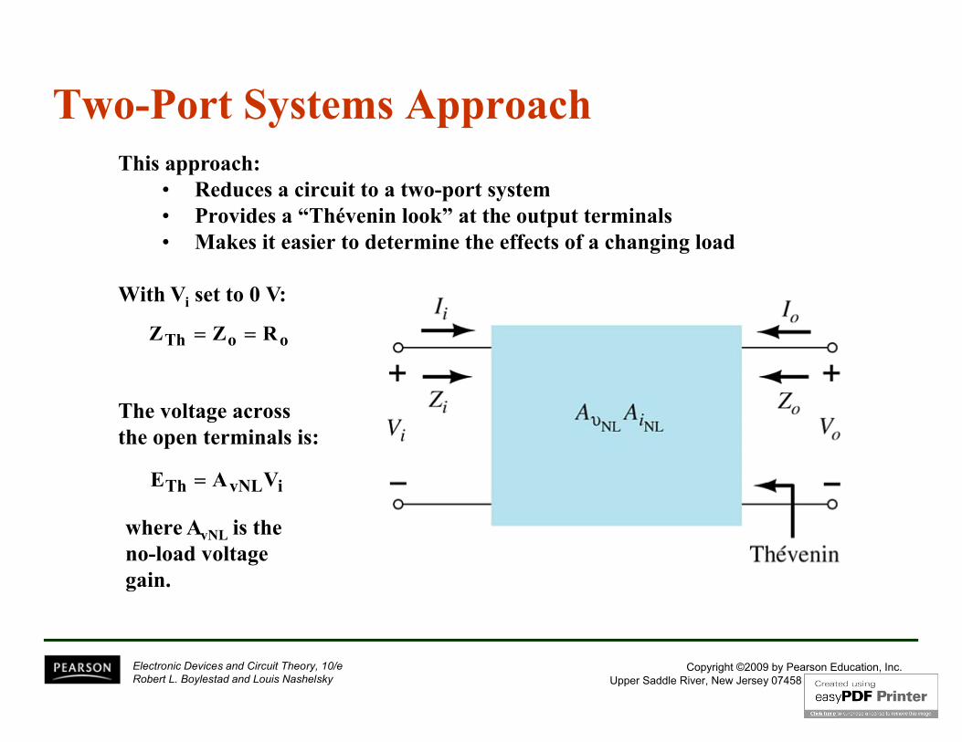
Two-Port Systems ApproachThis approach:
• Reduces a circuit to a two-port system• Provides a “Thévenin look” at the output terminals• Makes it easier to determine the effects of a changing load
ooTh RZZ
ivNLTh VAE
With Vi set to 0 V:
The voltage across the open terminals is:
where AvNL is the no-load voltage gain.

Copyright ©2009 by Pearson Education, Inc.Upper Saddle River, New Jersey 07458 • All rights reserved.
Electronic Devices and Circuit Theory, 10/eRobert L. Boylestad and Louis Nashelsky
Effect of Load Impedance on Gain
L
ivi R
ZAA
This model can be applied to any current- or voltage-controlled amplifier.
Adding a load reduces the gain of the amplifier:
vNLoL
L
i
ov A
RR
R
V
VA

Copyright ©2009 by Pearson Education, Inc.Upper Saddle River, New Jersey 07458 • All rights reserved.
Electronic Devices and Circuit Theory, 10/eRobert L. Boylestad and Louis Nashelsky
Effect of Source Impedance on Gain
si
sii RR
VRV
The fraction of applied signal that reaches the input of the amplifier is:
vNLsi
i
s
ovs A
RR
R
V
VA
The internal resistance of the signal source reduces the overall gain:

Copyright ©2009 by Pearson Education, Inc.Upper Saddle River, New Jersey 07458 • All rights reserved.
Electronic Devices and Circuit Theory, 10/eRobert L. Boylestad and Louis Nashelsky
Combined Effects of RS and RL on Voltage Gain
Effects of RL:
Effects of RL and RS:
L
ivi
oL
vNLL
i
ov
R
RAA
RR
AR
V
VA
L
isvsis
vNLoL
L
si
i
s
ovs
R
RRAA
ARR
R
RR
R
V
VA

Copyright ©2009 by Pearson Education, Inc.Upper Saddle River, New Jersey 07458 • All rights reserved.
Electronic Devices and Circuit Theory, 10/eRobert L. Boylestad and Louis Nashelsky
Cascaded Systems
• The output of one amplifier is the input to the next amplifier• The overall voltage gain is determined by the product of gains of the
individual stages• The DC bias circuits are isolated from each other by the coupling
capacitors• The DC calculations are independent of the cascading• The AC calculations for gain and impedance are interdependent

Copyright ©2009 by Pearson Education, Inc.Upper Saddle River, New Jersey 07458 • All rights reserved.
Electronic Devices and Circuit Theory, 10/eRobert L. Boylestad and Louis Nashelsky
R-C Coupled BJT Amplifiers
This image cannot currently be displayed.
Co RZ
Input impedance, first stage:
Output impedance, second stage:
Voltage gain:
e21i r||R||RZ
2v1vv
e
C2V
e
e21C1v
AAA
r
RA
r
r||R||R||RA

Copyright ©2009 by Pearson Education, Inc.Upper Saddle River, New Jersey 07458 • All rights reserved.
Electronic Devices and Circuit Theory, 10/eRobert L. Boylestad and Louis Nashelsky
R-C Coupled BJT AmplifiersDraw the ac equivalent circuit and calculate the voltage gain, input resistance andoutput resistance for the cascade BJT amplifier in above Figure. Let the parametersare:
Solution
Dc Analysis
kRRkRRkRRkRR EECC 1,2.2,7.4,15 21214231
0)(21 ,7.0,200,20 rVVVV ONBEQQCC
mAI
AI
CQ
BQ
979.3
89.19
1
1
mAI
AI
CQ
BQ
979.3
89.19
2
2
k307.12211 ee rr

Copyright ©2009 by Pearson Education, Inc.Upper Saddle River, New Jersey 07458 • All rights reserved.
Electronic Devices and Circuit Theory, 10/eRobert L. Boylestad and Louis Nashelsky
R-C Coupled BJT AmplifiersAc Analysis:The voltage gain at Q1 is:
The voltage gain at Q2 is
The overall gain is then,
The input resistance is:
The o/p resistance is:
06.102)36.957//2.2(153.01 kAV
6.336)2.2(153.02 kAV
353,34)6.336)(06.102(21 VVV AAA
36.957//// 21 ei BrRRR
kRR Co 2.22

Copyright ©2009 by Pearson Education, Inc.Upper Saddle River, New Jersey 07458 • All rights reserved.
Electronic Devices and Circuit Theory, 10/eRobert L. Boylestad and Louis Nashelsky
Cascode Connection
This example is a CE–CB combination. This arrangement provides high input impedance but a low voltage gain.
The low voltage gain of the input stage reduces the Miller input capacitance, making this combination suitable for high-frequency applications.

Copyright ©2009 by Pearson Education, Inc.Upper Saddle River, New Jersey 07458 • All rights reserved.
Electronic Devices and Circuit Theory, 10/eRobert L. Boylestad and Louis Nashelsky
Cascode Connection

Copyright ©2009 by Pearson Education, Inc.Upper Saddle River, New Jersey 07458 • All rights reserved.
Electronic Devices and Circuit Theory, 10/eRobert L. Boylestad and Louis Nashelsky
Darlington Connection
The Darlington circuit provides a very high current gain—the product of the individual current gains:
bD = b1b2
The practical significance is that the circuit provides a very high input impedance.

Copyright ©2009 by Pearson Education, Inc.Upper Saddle River, New Jersey 07458 • All rights reserved.
Electronic Devices and Circuit Theory, 10/eRobert L. Boylestad and Louis Nashelsky
DC Bias of Darlington Circuits
This image cannot currently be displayed.
BDBDE II)1(I
EEE RIV
EDB
BECCB RR
VVI
Base current:
Emitter current:
Emitter voltage:
Base voltage:
BEEB VVV

Copyright ©2009 by Pearson Education, Inc.Upper Saddle River, New Jersey 07458 • All rights reserved.
Electronic Devices and Circuit Theory, 10/eRobert L. Boylestad and Louis Nashelsky
AC small signal of Darlington Circuits

Copyright ©2009 by Pearson Education, Inc.Upper Saddle River, New Jersey 07458 • All rights reserved.
Electronic Devices and Circuit Theory, 10/eRobert L. Boylestad and Louis Nashelsky
Feedback Pair
This is a two-transistor circuit that operates like a Darlington pair, but it is not a Darlington pair.
It has similar characteristics: • High current gain• Voltage gain near unity• Low output impedance• High input impedance
The difference is that a Darlington uses a pair of like transistors, whereas the feedback-pair configuration uses complementary transistors.

Copyright ©2009 by Pearson Education, Inc.Upper Saddle River, New Jersey 07458 • All rights reserved.
Electronic Devices and Circuit Theory, 10/eRobert L. Boylestad and Louis Nashelsky
DC Analysis of Feedback Pair

Copyright ©2009 by Pearson Education, Inc.Upper Saddle River, New Jersey 07458 • All rights reserved.
Electronic Devices and Circuit Theory, 10/eRobert L. Boylestad and Louis Nashelsky
AC Analysis of Feedback Pair

Copyright ©2009 by Pearson Education, Inc.Upper Saddle River, New Jersey 07458 • All rights reserved.
Electronic Devices and Circuit Theory, 10/eRobert L. Boylestad and Louis Nashelsky
Current Mirror Circuits
Current mirror circuits provide constant current in integrated circuits.

Copyright ©2009 by Pearson Education, Inc.Upper Saddle River, New Jersey 07458 • All rights reserved.
Electronic Devices and Circuit Theory, 10/eRobert L. Boylestad and Louis Nashelsky
Current Mirror Example
Find I?

Copyright ©2009 by Pearson Education, Inc.Upper Saddle River, New Jersey 07458 • All rights reserved.
Electronic Devices and Circuit Theory, 10/eRobert L. Boylestad and Louis Nashelsky
Current Mirror More Configurations

Copyright ©2009 by Pearson Education, Inc.Upper Saddle River, New Jersey 07458 • All rights reserved.
Electronic Devices and Circuit Theory, 10/eRobert L. Boylestad and Louis Nashelsky
Current Source CircuitsConstant-current sources can be built using FETs, BJTs, and combinations of these devices.
IE IC
E
BEZE R
VVII
more…

Copyright ©2009 by Pearson Education, Inc.Upper Saddle River, New Jersey 07458 • All rights reserved.
Electronic Devices and Circuit Theory, 10/eRobert L. Boylestad and Louis Nashelsky
Current Source Circuits
VGS = 0VID = IDSS = 10 mA