
CHAPTER 3 FPGA IMPLEMENTATION USING VERILOG...
30
75 CHAPTER 3 FPGA IMPLEMENTATION USING VERILOG 3.1. INTRODUCTION TO VERILOG: The Verilog Hardware Description Language is a language for describing the behavior and structure of electronic circuits, and is an IEEE standard (IEEE Std. 1364-1995). Verilog is used to simulate the functionality of digital electronic circuits at levels of abstraction ranging from stochastic and pure behavior down to gate and switch level, and is also used to synthesize (i.e. automatically generate) gate level descriptions from more abstract Register Transfer Level descriptions. Verilog is commonly used to support the high level design (or language based design) process, in which an electronic design is verified by means of thorough simulation at a high level of abstraction before proceeding to detailed design using automatic synthesis tools. Verilog is also widely used for gate level verification of ICs (Integrated Circuits), including simulation, fault simulation and timing verification. The Verilog HDL was originally developed together with the Verilog-XL simulator by Gateway Design Automation, and introduced in 1984. In 1989 Cadence Design Systems acquired Gateway, and with it the rights to the Verilog language and the Verilog-XL simulator. In 1990 Cadence placed the Verilog language (but not Verilog-XL) into the public domain. A non-profit making organization, Open Verilog International (OVI) was formed with the task of taking the language through the IEEE standardization procedure, and Verilog became an IEEE standard in 1995. OVI will continue to maintain and develop the language. An hierarchical portion of a hardware design is described in Verilog by a Module. The Module defines both the interface to the block of hardware (i.e. the inputs and outputs) and its internal structure or behavior. A number of primitives, or Gates, are built into the Verilog language. They represent basic logic gates (e.g. and, or). In addition User Defined Primitives (UDPs) may be defined [81]. The structure of an electronic circuit is described by making Instances of
Transcript of CHAPTER 3 FPGA IMPLEMENTATION USING VERILOG...

75
CHAPTER 3
FPGA IMPLEMENTATION USING VERILOG
3.1. INTRODUCTION TO VERILOG:
The Verilog Hardware Description Language is a language for describing the
behavior and structure of electronic circuits, and is an IEEE standard (IEEE Std.
1364-1995).
Verilog is used to simulate the functionality of digital electronic circuits at
levels of abstraction ranging from stochastic and pure behavior down to gate and
switch level, and is also used to synthesize (i.e. automatically generate) gate level
descriptions from more abstract Register Transfer Level descriptions. Verilog is
commonly used to support the high level design (or language based design) process,
in which an electronic design is verified by means of thorough simulation at a high
level of abstraction before proceeding to detailed design using automatic synthesis
tools. Verilog is also widely used for gate level verification of ICs (Integrated
Circuits), including simulation, fault simulation and timing verification.
The Verilog HDL was originally developed together with the Verilog-XL
simulator by Gateway Design Automation, and introduced in 1984. In 1989 Cadence
Design Systems acquired Gateway, and with it the rights to the Verilog language and
the Verilog-XL simulator. In 1990 Cadence placed the Verilog language (but not
Verilog-XL) into the public domain. A non-profit making organization, Open
Verilog International (OVI) was formed with the task of taking the language through
the IEEE standardization procedure, and Verilog became an IEEE standard in 1995.
OVI will continue to maintain and develop the language.
An hierarchical portion of a hardware design is described in Verilog by a
Module. The Module defines both the interface to the block of hardware (i.e. the
inputs and outputs) and its internal structure or behavior. A number of primitives, or
Gates, are built into the Verilog language. They represent basic logic gates (e.g. and,
or). In addition User Defined Primitives (UDPs) may be defined [81].
The structure of an electronic circuit is described by making Instances of
76
Modules and Primitives (UDPs and Gates) within a higher level Module, and
connecting the Instances together using Nets. A Net represents an electrical
connection, a wire or a bus. A list of Port connections is used to connect Nets to the
Ports of a Module or Primitive Instance, where a Port represents a pin. Registers may
also be connected to the input Ports (only) of an Instance. Nets (and Registers) have
values formed from the logic values 0, 1, X (unknown or uninitialized) and Z (high
impedance or floating). In addition to logic values, Nets also have a Strength value.
Strengths are used extensively in switch level models, and to resolve situations where
a net has more than one driver.
The behavior of an electronic circuit is described using Initial and Always
constructs and Continuous Assignments. Along with UDPs and Gates these represent
the leaves in the hierarchy tree of the design. Each Initial, Always, Continuous
Assignment, UDP and Gate Instance executes concurrently with respect to all others,
but the Statements inside an Initial or Always are in many ways similar to the
statements in a software programming language. They are executed at times dictated
by Timing Controls, such as delays, and (simulation) event controls. Statements
execute in sequence in a Begin-End block, or in parallel in a Fork-Join block. A
Continuous Assignment modifies the values of Nets. An Initial or Always modifies
the values of Registers. An Initial or Always can be decomposed into named Tasks
and Functions, which can be given arguments. There are also a number of built in
System Tasks and Functions. The Programming Language Interface (PLI) is an
integral part of the Verilog language, and provides a means of calling functions
written in C in the same way as System Tasks and Functions.
Verilog source code is usually typed into one or more text files on a
computer. Those text files are then submitted to a Verilog compiler or interpreter
which builds the data files necessary for simulation or synthesis. Sometimes
simulation immediately follows compilation with no intermediate data files being
created [82].
Module Structure
module M (P1, P2, P3, P4);
input P1, P2;
output [7:0] P3;
77
inout P4;
reg [7:0] R1, M1[1:1024];
wire W1, W2, W3, W4;
parameter C1 = "This is a string";
initial
begin :BlockName
// Statements
end
always
begin
// Statements
end
// Continuous assignments...
assign W1 = Expression;
wire (Strong1, Weak0) [3:0] #(2,3) W2 = Expression;
// Module instances...
COMP U1 (W3, W4);
COMP U2 (.P1(W3), .P2(W4));
task T1;
input A1;
inout A2;
output A3;
begin
// Statements
end
endtask
function [7:0] F1;
input A1;
begin
// Statements
F1 = Expression;
end

78
endfunction
endmodule
Statements
#delay
wait (Expression)
@(A or B or C)
@(posedgeClk)
Reg = Expression;
Reg<= Expression;
VectorReg[Bit] = Expression;
VectorReg[MSB:LSB] = Expression;
Memory[Address] = Expression;
assignReg = Expression
deassignReg;
TaskEnable(...);
disableTaskOrBlock;
->EventName;
if (Condition)
...
else if (Condition)
...
else
...
case (Selection)
Choice1 :
...
Choice2, Choice3 :
...
default :
...
endcase

79
for (I=0; I<MAX; I=I+1)
...
repeat (8)
...
while (Condition)
...
forever
...
Coding standards are divided into two categories. Lexical coding standards,
which control text layout, naming conventions and commenting, are intended to
improve readability and ease of maintenance. Synthesis coding standards, which
control Verilog style, are intended to avoid common synthesis pitfalls and find
synthesis errors early in the design flow [83].
The following lists of coding standards will need to be modified according to
the choice of tools and personal preferences.
Lexical Coding Standards
Limit the contents of each Verilog source file to one module, and do not split
modules across files.
Source file names should relate to the file contents (e.g. Module Name .v).
Write only one declaration or statement per line.
Use indentation as shown in the examples.
Be consistent about the case of user defined names (e.g. first letter a capital).
User defined names should be meaningful and informative, although local
names (e.g. loop variables) may be terse.
Write comments to explain (not duplicate) the Verilog code. It is particularly
important to comment interfaces (e.g. module parameters, ports, task and
function arguments).
Use parameters or `define macros wherever possible, instead of directly
embedding literal numbers and strings in declarations and statements.
80
Synthesis Coding Standards
Partition the design into small functional blocks, and use a behavioral style
for each block. Avoid gate level descriptions except for critical parts of the
design.
Have a well defined clocking strategy, and implement that strategy explicitly
in Verilog (e.g. single clock, multi-phase clocks, gated clocks, multiple clock
domains). Ensure that clock and reset signals in Verilog are clean (i.e. not
generated from combinational logic or unintentionally gated).
Have a well defined (manufacturing) testing strategy, and code up the Verilog
appropriately (e.g. all flip flops resettable, test access from external pins, no
functional redundancy).
Every Verilog always should conform to one of the standard synthesizable
process templates.
An always describing combinational and latched logic must have all of the
inputs in the event control list at the top of the always.
A combinational always must not contain incomplete assignments, i.e. all
outputs must be assigned for all combinations of input values. An always
describing combinational and latched logic must not contain feedback, i.e.
registers assigned as outputs from the always must not be read as inputs to the
always.
A clocked always must have only the clock and any asynchronous control
inputs (usually reset or set) in the event control list.
Avoid unwanted latches. Unwanted latches are caused by incomplete
assignments in an un clocked always.
Avoid unwanted flip flops. Flip flops are synthesized when registers are
assigned in a clocked always using a non-blocking assignment, or when
registers retain their value between successive iterations of a clocked always
and thus between clock cycles).
All internal state registers must be resettable, in order that the Register
Transfer Level and gate level descriptions can be reset into the same known
state for verification. (This does not apply to pipeline or synchronization

81
registers.)
For finite state machines and other sequential circuits with unreachable states
(e.g. a 4 bit decade counter has 6 unreachable states), if the behavior of the
hardware in such states is to be controlled, then the behavior in all 2N
possible states must be described explicitly in Verilog, including the behavior
in unreachable states. This allows safe state machines to be synthesized.
Avoid delays in assignments, except where necessary to solve the problem of
zero delay clock skew at Register Transfer Level.
Do not use registers of type integer or time, otherwise they will synthesize to
32 bit busses and 64 bit busses respectively.
Check carefully any Verilog code which uses dynamic indexing (i.e. a bit
select or memory element using a variable index or address), loop statements,
or arithmetic operators, because such code can synthesize to large numbers of
gates which can be hard to optimize [84].
Design Flow
The basic flow for using Verilog and synthesis to design an Application
Specific IC (ASIC) or complex FPGA is shown below. Iteration around the design
flow is necessary, but is not shown here. Also, the design flow must be modified
according to the kind of device being designed and the specific application [85].
� 1 System analysis and specification
� System partitioning
Top level block capture
Block size estimation
Initial floor planning
� Block level design. For each block:
Write Register Transfer Level Verilog
Synthesis coding checks
Write Verilog test fixture
Verilog simulation
Write synthesis scripts - constraints, boundary conditions, hierarchy
Initial synthesis - analysis of gate count and timing
82
� Chip integration. For complete chip:
Write Verilog test fixture
Verilog simulation
Synthesis
Gate level simulation
� Test generation
Modify gate level netlist for test
Generate test vectors
Simulate testable netlist
� Place and route (or fit) chip
� Post layout simulation, fault simulation and timing analysis.
3.2 PROGRAMMING IN VERILOG:
Entry of large digital designs at the schematic level is very time consuming
and can be exceedingly tedious for circuits with wide data paths that must be
repeated for each bit of the data path. Hardware description languages (HDLs)
provide a more compact textual description of a design. Verilog is a powerful
language and offers several different levels of descriptions. The lowest level is the
gate level, in which statements are used to define individual gates. In the structural
level, more abstract assign statements and always blocks are used. These constructs
are more powerful and can describe a design with fewer lines of code, but still
provide a clearly defined relationship to actual hardware. The behavioral level of
description is the most abstract, resembling C with function calls (called tasks), for
and while loops, etc. Behavioral modeling describes what a design must do, but does
not have an obvious mapping to hardware [86].
This Verilog documentation will focus on the structural level of description
because it is efficient to code, yet offers a predictable mapping to hardware in the
hands of a skilled user. A synthesis tool is used to translate the Verilog into actual
hardware, such as logic gates on a custom ASIC or configurable logic blocks (CLBs)
on a Field Programmable Gate Array (FPGA). When you use Verilog to describe
hardware that you will actually construct, it is extremely important to know what
gates your code will describe. Otherwise, you are almost guaranteed to get something

83
that you didn’t want. Sometimes this means extra latches appearing in your circuit in
places you didn’t expect. Other times, it means that the circuit is much slower than
required or takes far more gates than it would if more carefully described.
Unfortunately, FPGA synthesis tools do not directly show you the gates synthesized
from your code. Therefore, it is particularly easy to get into trouble and that much
more important to understand what gates your code is implying [87].
There are two kinds of statements used to model logic. Continuous
assignment statements always imply combinational logic. Always blocks can imply
combinational logic or sequential logic, depending how they are used. It is critical to
partition your design into combinational and sequential components and write
Verilog in such a way that you get what you want. If you don’t know whether a
block of logic is combinational or sequential, you are very likely to get the wrong
thing. A particularly common mistake is to use always blocks to model
combinational logic, but to accidentally imply latches or flip-flops [88].
3.2.1 Modeling with Continuous Assignments
With schematics, a 32-bit adder is a complex design. It can be constructed
from 32 full adder cells, each of which in turn requires about six 2-input gates.
Verilog provides a much more compact description:
module adder(a, b, y);
input [31:0] a, b;
output [31:0] y;
assign y = a + b;
endmodule
A Verilog module is like a “cell” or “macro” in schematics. It begins with a
description of the inputs and outputs, which in this case are 32 bit busses. In the
structural description style, the module may contain assign statements, always
blocks, or calls to other modules [89].
During simulation, an assign statement causes the left hand side (y) to be
updated any time the right side (a/b) changes. This necessarily implies combinational
84
logic; the output on the left side is a function of the current inputs given on the right
side. A 32-bit adder is a good example of combinational logic [90].
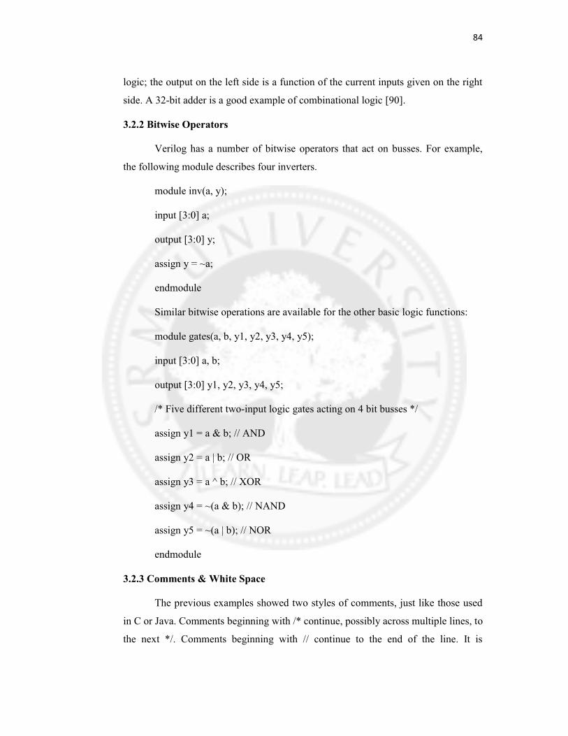
3.2.2 Bitwise Operators
Verilog has a number of bitwise operators that act on busses. For example,
the following module describes four inverters.
module inv(a, y);
input [3:0] a;
output [3:0] y;
assign y = ~a;
endmodule
Similar bitwise operations are available for the other basic logic functions:
module gates(a, b, y1, y2, y3, y4, y5);
input [3:0] a, b;
output [3:0] y1, y2, y3, y4, y5;
/* Five different two-input logic gates acting on 4 bit busses */
assign y1 = a & b; // AND
assign y2 = a | b; // OR
assign y3 = a ^ b; // XOR
assign y4 = ~(a & b); // NAND
assign y5 = ~(a | b); // NOR
endmodule
3.2.3 Comments & White Space
The previous examples showed two styles of comments, just like those used
in C or Java. Comments beginning with /* continue, possibly across multiple lines, to
the next */. Comments beginning with // continue to the end of the line. It is

85
important to properly comment complex logic so you can understand what you did
six months from now or so that some poor slob assigned to fix your buggy code will
be able to figure it out rather than calling you at 2 am with a question [91].
Verilog is not picky about the use of white space. Nevertheless, proper
indenting and spacing is very helpful to make nontrivial designs readable. Verilog is
case-sensitive. Be consistent in your use of capitalization and underscores in signal
and module names [92].
3.2.4 Reduction Operators
Reduction operators imply a multiple-input gate acting on a single bus. For
example, the following module describes an 8-input AND gate with inputs A[0],
A[1], A[2], … , A[7].
module and8(a, y);
input [7:0] a;
output y;
assign y = &a;
endmodule
As one would expect, |, ^, ~&, and ~| reduction operators are available for
OR, XOR, NAND, and NOR as well. Recall that a multi-bit XOR performs parity,
returning true if an odd number of inputs are true [93].
3.2.5 Other Operators
The conditional operator ?: works like the same operator in C or Java and is
very useful for describing multiplexers. It is called a ternary operator because it takes
three inputs. If the first input is nonzero, the result is the expression in the second
input. Otherwise, the result is the expression in the third input.
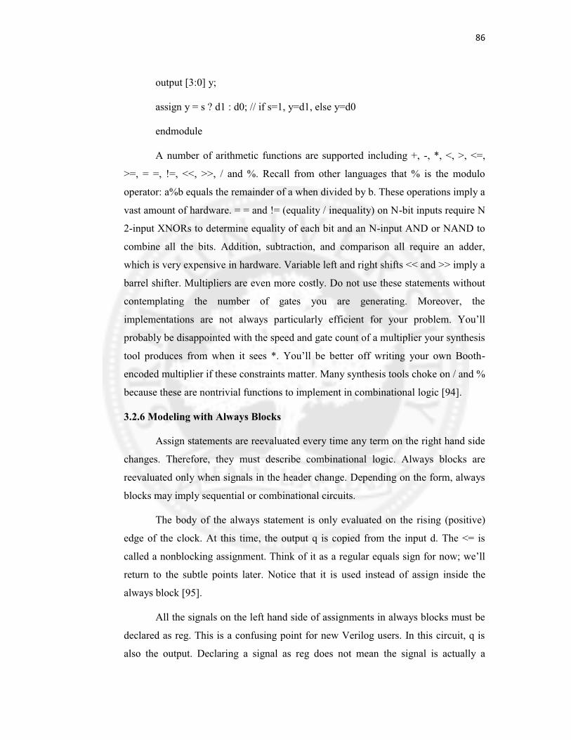
module mux2(d0, d1, s, y);
input [3:0] d0, d1;
input s;
86
output [3:0] y;
assign y = s ? d1 : d0; // if s=1, y=d1, else y=d0
endmodule
A number of arithmetic functions are supported including +, -, *, <, >, <=,
>=, = =, !=, <<, >>, / and %. Recall from other languages that % is the modulo
operator: a%b equals the remainder of a when divided by b. These operations imply a
vast amount of hardware. = = and != (equality / inequality) on N-bit inputs require N
2-input XNORs to determine equality of each bit and an N-input AND or NAND to
combine all the bits. Addition, subtraction, and comparison all require an adder,
which is very expensive in hardware. Variable left and right shifts << and >> imply a
barrel shifter. Multipliers are even more costly. Do not use these statements without
contemplating the number of gates you are generating. Moreover, the
implementations are not always particularly efficient for your problem. You’ll
probably be disappointed with the speed and gate count of a multiplier your synthesis
tool produces from when it sees *. You’ll be better off writing your own Booth-
encoded multiplier if these constraints matter. Many synthesis tools choke on / and %
because these are nontrivial functions to implement in combinational logic [94].
3.2.6 Modeling with Always Blocks
Assign statements are reevaluated every time any term on the right hand side
changes. Therefore, they must describe combinational logic. Always blocks are
reevaluated only when signals in the header change. Depending on the form, always
blocks may imply sequential or combinational circuits.
The body of the always statement is only evaluated on the rising (positive)
edge of the clock. At this time, the output q is copied from the input d. The <= is
called a nonblocking assignment. Think of it as a regular equals sign for now; we’ll
return to the subtle points later. Notice that it is used instead of assign inside the
always block [95].
All the signals on the left hand side of assignments in always blocks must be
declared as reg. This is a confusing point for new Verilog users. In this circuit, q is
also the output. Declaring a signal as reg does not mean the signal is actually a

87
register! All it means is it appears on the left side in an always block. We will see
examples of combinational signals later that are declared reg but have no flip-flops.
At startup, the q output is initialized to ’x. Generally, it is good practice to use
flip-flops with reset inputs so that on power-up you can put your system in a known
state. The reset may be either asynchronous or synchronous. Asynchronous resets
occur immediately. Synchronous resets only change the output on the rising edge of
the clock. Xilinx FPGAs have dedicated internal hardware to support initializing
asynchronously resettable flip-flops on startup, so such flops are preferred [96].
module flop(clk, d, q);
input clk;
input [3:0] d;
output [3:0] q;
reg [3:0] q;
always @(posedge clk)
q <= d;
endmodule
3.3 CIRCUIT DESIGN USING VERILOG:
HDL and FPGA devices allow designers to quickly develop and simulate a
sophisticated digital circuit, realize it on a prototyping device, and verify operation of
the physical implementation [97]. As these technologies mature, they have become
mainstream practice. We can now use a PC and an inexpensive FPGA prototyping
board to construct a complex and sophisticated digital system. This book uses a
"learning by doing" approach and illustrates the FPGA and HDL development and
design process by a series of examples. A wide range of examples is included, from a
simple gate-level circuit to an embedded system with an 8-bit soft-core
microcontroller and customized I/O peripherals. All examples can be synthesized and
physically tested on a prototyping board [98].
88
3.3.1 Gate-Level Combinational Circuit
Verilog is a hardware description language. It was developed in the mid-
1980s and later transferred to the IEEE (Institute of Electrical and Electronics
Engineers). The language is formally defined by IEEE Standard 1364. The standard
was ratified in 1995 (referred to as Verilog- 1995) and revised in 2001 (referred to as
Verilog-2001). Many useful enhancements are added in the revised version. We use
Verilog-2001 in this work. Verilog is intended for describing and modeling a digital
system at various levels and is an extremely complex language [99].
Although the syntax of Verilog is somewhat like that of the C language, its
semantics (i.e., "meaning") is based on concurrent hardware operation and is totally
different from the sequential execution of C. The subtlety of some language
constructs and certain inherent non-deterministic behavior of Verilog can lead to
difficult-to-detect errors and introduce a discrepancy between simulation and
synthesis [100]. The coding of this book follows a "better safe-than-buggy"
philosophy. Instead of writing quick and short codes, the focus is on style and
constructs that are clear and synthesizable and can accurately describe the desired
hardware.
Table 3.1 Truth table of 1-bit equality comparator
Input
i0 i1
Output
eq
0 0 1
0 1 0
1 0 0
1 1 1
Consider a 1-bit equality comparator with two inputs, i0 and i1 and an output,
eq. The eq signal is asserted when i0 and i1 are equal. The truth table of this circuit is
shown in Table 3.1.
Assume that we want to use basic logic gates, which include not, and, or, and
xor cells, to implement the circuit [101]. One way to describe the circuit is to use a
sum-of-products format. The logic expression is

89
eq = i0.i1 + io’.i1’
One possible Verilog code is shown in Table 3.2. We examine the language
constructs and statements of this code in the following subsections.
Table 3.2 Gate-level implementation of a 1-bit comparator
module e q l
// I/O p o r t s
(
input wire iO, il,
5 output w i r e eq
) ;
// s i g n a l d e c l a r a t i o n
wire PO, pl;
10
// body
// slim o f two p r o d u c t t e r m s
a s s i g n eq = pO I pl;
// p r o d u c t t e r m s
is a s s i g n pO = -iO & -il;
a s s i g n pl = iO & i l ;
endmodule
Figure 3.1: Graphical representation of a Comparator program
The best way to understand an HDL (hardware description language)
program is to think in terms of hardware circuits. This program consists of three
portions. The I/O port portion describes the input and output ports of this circuit,

90
which are i0 and il, and eq, respectively [102]. The signal declaration portion
specifies the internal connecting signals, which are p0 and pl. The body portion
describes the internal organization of the circuit. There are three continuous
assignments in this code. Each can be thought of as a circuit part that performs
certain simple logical operations [103].
The graphical representation of this program is shown in Figure 3.1. The three
continuous assignments constitute the three circuit parts. The connections among
these parts are specified implicitly by the signal and port names.
3.4 OVERVIEW OF FPGA
Developing a large FPGA-based system is an involved process that consists
of many complex transformations and optimization algorithms. Software tools are
needed to automate some of the tasks. We use the Web version of the Xilinx ISE
package for synthesis and implementation, and use the starter version of Mentor
Graphics ModelSim XE III package for simulation. In this section, we give a brief
overview of the FPGA device and the S3 prototyping board, and provide short
tutorials for the two software packages to "jump-start" the learning process [104].
3.4.1 Overview of a general FPGA device
A FPGA is a logic device that contains a two-dimensional array of generic
logic cells and programmable switches [105]. The conceptual structure of an FPGA
device is shown in Figure 3.2. A logic cell can be configured (i.e., programmed) to
perform a simple function, and a programmable switch can be customized to provide
interconnections among the logic cells [106]. A custom design can be implemented
by specifying the function of each logic cell and selectively setting the connection of
each programmable switch. Once the design and synthesis are completed, we can use
a simple adaptor cable to download the desired logic cell and switch configuration to
the FPGA device and obtain the custom circuit. Since this process can be done "in
the field" rather than "in a fabrication facility (fab)," the device is known as field
programmable [107].

91
Figure 3.2 Conceptual structure of an FPGA device
Figure 3.3 Three-input LUT-based logic cell.
LUT based logic cell: A logic cell usually contains a small configurable
combinational circuit with a D-type flip-flop (D FF). The most common method to
implement a configurable combinational circuit is a look-up table (LUT). An n-input
LUT can be considered as a small 2n-by-1 memory. By properly writing the memory
content, we can use an LUT to implement any n-input combinational function [108].
The conceptual diagram of a three input LUT-based logic cell is shown in Figure 3.3.
Note that the output of the LUT can be used directly or stored to the D FF. The latter
can be used to implement sequential circuits [109].

92
Macrocell: Most FPGA devices also embed certain macro cells or macro blocks.
These are designed and fabricated at the transistor level, and their functionalities
complement the general logic cells [110]. Commonly used macro cells include
memory blocks, combinational multipliers, clock management circuits, and 110
interface circuits. Advanced FPGA devices may even contain one or more
prefabricated processor cores [111].
3.4.2 Overview of the Xilinx Spartan3 devices
This work uses Xilinx Spartan-3 family FPGA devices. Based on the ratio
between the number of logic cells and the I/O counts, the family is further divided
into several subfamilies. Our discussion applies to all the subfamilies [112].
Logic cell, slice, and CLB: The most basic element of the Spartan-3 device is a
logic cell (LC), which contains a four-input LUT and a D FF, similar to that in
Figure 3.3. In addition, a logic cell contains a carry circuit, which is used to
implement arithmetic functions, and a multiplexing circuit, which is used to
implement wide multiplexers. The LUT can also be configured as a 16-by- 1 static
random access memory (SRAM) or a 16-bit shift register.
To increase flexibility and improve performance, eight logic cells are
combined with a special internal routing structure. In Xilinx terms, two logic cells
are grouped to form a slice, and four slices are grouped to form a configurable logic
block (CLB) [113].
Macro cell: The Spartan-3 device contains four types of macro blocks:
combinational multiplier, block RAM, digital clock manager (DCM), and
input/output block (IOB). The combinational multiplier accepts two 18-bit numbers
as inputs and calculates the product. The block RAM is an 18K-bit synchronous
SRAM that can be arranged in various types of configurations. A DCM uses a
digital-delayed loop to reduce clock skew and to control the frequency and phase
shift of a clock signal. An IOB controls the flow of data between the device's I/O
pins and the internal logic. It can be configured to support a wide variety of I/O
signaling standards.
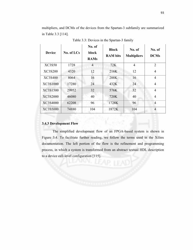
Devices in the Spartan-3 subfamily: Although Spartan-3 FPGA devices have
similar types of logic cells and macro cells, their densities differ. Each subfamily
contains an array of devices of various densities. The numbers of LCs, block RAMS,
93
multipliers, and DCMs of the devices from the Spartan-3 subfamily are summarized
in Table 3.3 [114].
Table 3.3: Devices in the Spartan-3 family
Device No. of LCs
No. of
block
RAMs
Block
RAM bits
No. of
Multipliers
No. of
DCMs
XC3S50 1728 4 72K 4 2
XC3S200 4320 12 216K 12 4
XC3S400 8064 16 288K 16 4
XC3S1000 17280 24 432K 24 4
XC3S1500 29952 32 576K 32 4
XC3S2000 46080 40 720K 40 4
XC3S4000 62208 96 1728K 96 4
XC3S5000 74880 104 1872K 104 4
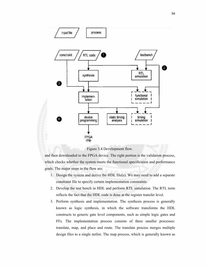
3.4.3 Development Flow
The simplified development flow of an FPGA-based system is shown in
Figure 3.4. To facilitate further reading, we follow the terms used in the Xilinx
documentation. The left portion of the flow is the refinement and programming
process, in which a system is transformed from an abstract textual HDL description
to a device cell-level configuration [115].
94
Figure 3.4 Development flow.
and then downloaded to the FPGA device. The right portion is the validation process,
which checks whether the system meets the functional specification and performance
goals. The major steps in the flow are:
1. Design the system and derive the HDL file(s). We may need to add a separate
constraint file to specify certain implementation constraints.
2. Develop the test bench in HDL and perform RTL simulation. The RTL term
reflects the fact that the HDL code is done at the register transfer level.
3. Perform synthesis and implementation. The synthesis process is generally
known as logic synthesis, in which the software transforms the HDL
constructs to generic gate level components, such as simple logic gates and
FFs. The implementation process consists of three smaller processes:
translate, map, and place and route. The translate process merges multiple
design files to a single netlist. The map process, which is generally known as

95
technology mapping, maps the generic gates in the netlist to FPGA's logic
cells and IOBs. The place and route process, which is generally known as
placement and routing, derives the physical layout inside the FPGA chip. It
places the cells in physical locations and determines the routes to connect
various signals. In the Xilinx flow, static timing analysis, which determines
various timing parameters, such as maximal propagation delay and maximal
clock frequency, is performed at the end of the implementation process.
4. Generate and download the programming file. In this process, a configuration
file is generated according to the final netlist. This file is downloaded to an
FPGA device serially to configure the logic cells and switches. The physical
circuit can be verified accordingly [116].
The optional functional simulation can be performed after synthesis, and the
optional timing simulation can be performed after implementation. Functional
simulation uses a synthesized netlist to replace the RTL description and checks the
correctness of the synthesis process. Timing simulation uses the final netlist, along
with detailed timing data, to perform simulation. Because of the complexity of the
netlist, functional and timing simulation may require a significant amount of time
[117]. If we follow good design and coding practices, the HDL code will be
synthesized and implemented correctly. We only need to use RTL simulation to
check the correctness of the HDL code and use static timing analysis to examine the
relevant timing information. Both functional and timing simulations may be omitted
from the development flow.
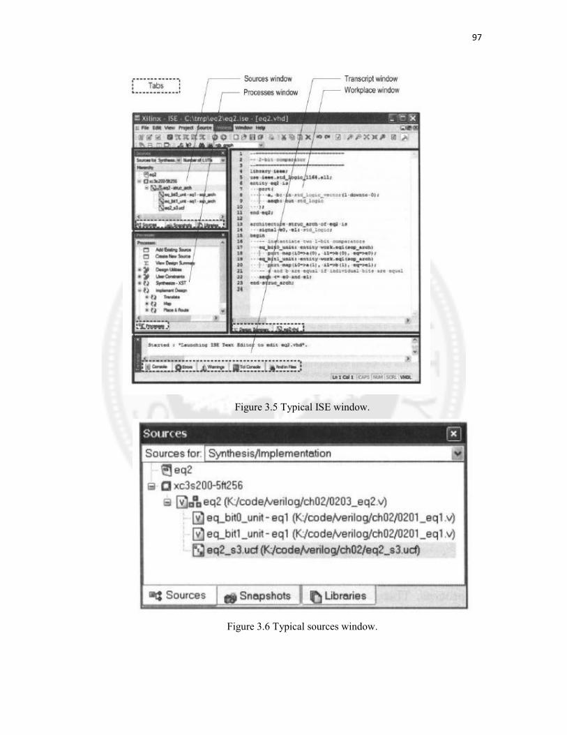
3.4.4 Overview of the XILLNX ISE Project Navigator
Xilinx ISE (integrated software environment) controls all aspects of the
development flow. Project Navigator is a graphical interface for users to access
software tools and relevant files associated with a project. We use it to launch all
development tasks except ModelSim simulation [118]. The discussion in this section
and the tutorial in the next section are based on ISE WebPack version 8.2.
The default ISE window is shown in Figure 3.5. It is divided into four
subwindows:
Sources window (top left): hierarchically displays the files included in the project

96
Processes window (middle left): displays available processes for the source file
currently selected
Transcript window (bottom): displays status messages, errors, and warnings
Workplace window (top right): contains multiple document windows (such as HDL
code, report, schematic, and so on) for viewing and editing
Each subwindow may be resized, moved, docked, or undocked. The default layout
can be restored by selecting View + Restore. Note that a subwindow may contain
multiple pages. The tabs at the bottom are used to select the desired page.
Sources window The sources window is used mainly to display files associated with
the current project. A typical sources window is shown in Figure 3.6. The top drop-
down list, labeled Sources for:, specifies the current design view. The
synthesis/implementation view should be selected since we use ISE only for
synthesis and implementation. There are three tabs at the bottom, labeled Sources,
Snapshots, and Libraries. The Sources tab displays the project name, the FPGA
device specified, and user documents and design files. The modules are displayed
according to the internal design hierarchy. In Figure 3.6, the eq1 and eq2 entities are
shown. The eq2 module also includes the eq_s3.ucf file, which specifies the
constraints of the design. We can open a file in the workplace window by double-
clicking the corresponding module. A top-level module icon can be placed next to a
module, as in the eq2 module, to invoke synthesis and implementation for this
particular module. The Snapshots tab displays project's "snapshots," which are copies
of previously stored project files. The Libraries tab shows all libraries associated
with the project [119].
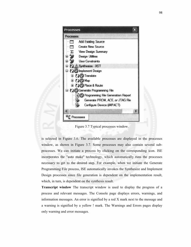
Processes window The processes window displays the processes available. The
display is context sensitive and the available processes are based on the source type
selected in the sources window. For example, the eq2 module, which is set as the
top-level module,
97
Figure 3.5 Typical ISE window.
Figure 3.6 Typical sources window.
98
Figure 3.7 Typical processes window.
is selected in Figure 3.6. The available processes are displayed in the processes
window, as shown in Figure 3.7. Some processes may also contain several sub-
processes. We can initiate a process by clicking on the corresponding icon. ISE
incorporates the "auto make" technology, which automatically runs the processes
necessary to get to the desired step. For example, when we initiate the Generate
Programming File process, ISE automatically invokes the Synthesize and Implement
Design processes since file generation is dependent on the implementation result,
which, in turn, is dependent on the synthesis result.
Transcript window The transcript window is used to display the progress of a
process and relevant messages. The Console page displays errors, warnings, and
information messages. An error is signified by a red X mark next to the message and
a warning is signified by a yellow ! mark. The Warnings and Errors pages display
only warning and error messages.
99
Workplace window The workplace window is for users to view and edit various
types of files. We use it to perform two main tasks. The first task is to view and edit
the HDL and constraint files. The default editor is the ISE Text Editor, which is a
simple text editor with features to assist creation of the HDL code. The second task is
to check the design summary and various reports [120].
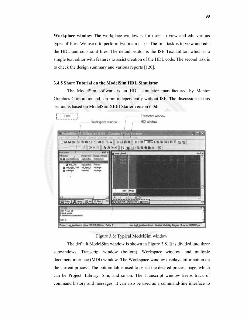
3.4.5 Short Tutorial on the ModelSim HDL Simulator
The ModelSim software is an HDL simulator manufactured by Mentor
Graphics Corporationand can run independently without ISE. The discussion in this
section is based on ModelSim XEIII Starter version 6.0d.
Figure 3.8: Typical ModelSim window
The default ModelSim window is shown in Figure 3.8. It is divided into three
subwindows: Transcript window (bottom), Workspace window, and multiple
document interface (MDI) window. The Workspace window displays information on
the current process. The bottom tab is used to select the desired process page, which
can be Project, Library, Sim, and so on. The Transcript window keeps track of
command history and messages. It can also be used as a command-line interface to

100
enter ModelSim commands. The MDI window is an area to display HDL text,
waveform, and so on. The bottom tab selects the desired pages. Each subwindow
may be resized, moved, docked, or undocked. Additional windows may appear for
some operations. The default layout can be restored by selecting Window + Initial
Layout.
We present a short tutorial in this section to illustrate the basic simulation
process. There are three steps:
1. Prepare a simulation project.
2. Compile the HDL codes.
3. Perform a simulation and examine the waveform.
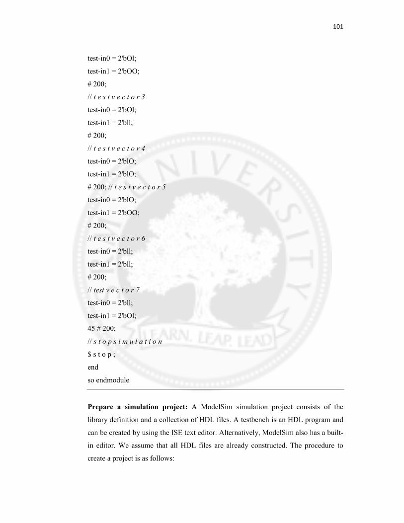
We use the 2-bit comparator for the tutorial, and the code is in Table 3.4 below.
Table 3.4 Testbench of a 2-bit comparator
// The ' t i m e s c a l e d i r e c t i v e s p e c i f i e s t h a t
// t h e .simlrlation t i m e u n i t i s 1 ns and
// t h e s i m u l a t i o n timestep i s 10 ps
' t i m e s c a l e 1 ns/lO ps
<
module eq2-testbench;
// sigrial d e c l a r a t i o n
r e g [I :0] test-in0 , test-in1 ;
wire test-out ;
I0 // instatitiate t h e circuit under t e s t
eq2 uut
(.a(test-inO), .b(test-inl), .aeqb(test-out));
15 // l e s t v e c t o r g e n e r a t o r
i n i t i a l
begin
// t e s t v e c t o r 1
test-in0 = 2'bOO;
test-in1 = 2'bOO;
# 200;
// l e s t v e c t o r 2
101
test-in0 = 2'bOl;
test-in1 = 2'bOO;
# 200;
// t e s t v e c t o r 3
test-in0 = 2'bOl;
test-in1 = 2'bll;
# 200;
// t e s t v e c t o r 4
test-in0 = 2'blO;
test-in1 = 2'blO;
# 200; // t e s t v e c t o r 5
test-in0 = 2'blO;
test-in1 = 2'bOO;
# 200;
// t e s t v e c t o r 6
test-in0 = 2'bll;
test-in1 = 2'bll;
# 200;
// test v e c t o r 7
test-in0 = 2'bll;
test-in1 = 2'bOl;
45 # 200;
// s t o p s i m u l a t i o n
$ s t o p ;
end
so endmodule
Prepare a simulation project: A ModelSim simulation project consists of the
library definition and a collection of HDL files. A testbench is an HDL program and
can be created by using the ISE text editor. Alternatively, ModelSim also has a built-
in editor. We assume that all HDL files are already constructed. The procedure to
create a project is as follows:

102
1. Select Start + All Programs + ModelSim XE Ill 6.0d + ModelSim (or
wherever ModelSim resides) to launch the ModelSim program.
2. Select File + New + Project and the Create Project dialog appears. Enter the
project name as eq-testbench, select the project location, and set Default
Library Name to work. Click OK. A blank Project page appears in the main
window and the Add items to the project dialog appears.
3. In the Add items to the project dialog, click Add Existing File and add the
necessary HDL files. Click OK. The project tab appears in the workplace
subwindow and displays the selected files.
Compile the HDL code: The compile term here means to convert the HDL code
into ModelSim internal format. In Verilog, compiling is done on the module basis.
The procedure is:
1. Highlight the eql file and right-click the mouse. Select Compile + Compile
Selected. Note that the compiling should be started from the modules at the
bottom of the design hierarchy. The progress and messages are displayed in
the transcript window.
2. If the file contains no syntactical error, a check mark shows up. Otherwise, an
X mark shows up. Click the red error line in the transcript window to locate
the errors. Correct the problems, save the file, and recompile the file.
3. Repeat the preceding steps to compile the eq2 file and then the eq-tb file.
Perform a simulation and examine the waveform: After compiling the test bench
and corresponding files, we can perform the simulation and examine the resulting
waveform. This corresponds to running the circuit in a virtual lab bench and
checking the waveform in a virtual logic analyzer. The procedure is:
1. Select Simulate + Simulate and the Simulate dialog appears.
2. In the Design tab, find and expand the work library, which is the one defined
when we create the project. All compiled units are displayed.
3. Load eq2-testbench by double-clicking the corresponding icon. The sim tab
appears in the workplace window and the corresponding page displays the
structure of the eq2-testbench module. An object window, which contains the
signals in the selected module, may also appear.

103
4. Highlight the uut unit and right-click the mouse. Select Add + Add to Wave.
This adds all the signals of the uut unit to the waveform page. The waveform
page appears in the MDI window.
5. If necessary, rearrange the signals order and set them to the proper formats
(decimal, hex, and so on).
6. Select Simulate + Run. There are several commands to control the
simulation: Restart (restart the simulation), Run (run the simulation one step),
Continue run (resume the run from the interrupt), Run All (run the simulation
forever), and Break (break the simulation). These commands are also shown
as icons at the top of the window.
7. The waveform window displays the simulated result. We can scroll the
window, zoom in, or zoom out to check the correctness of the design [121].
3.5 IMPLEMENTATION USING VERILOG:
The R22SDF presented above has been fully coded in Verilog HDL. Once the
design is coded in Verilog, the Modelsim XEIII6.2c compiler [120] and the Xilinx
Foundation ISA Environment 9.1i [121] generate a net-list for FPGA configuration. The
net-list can then be downloaded into the FPGA using the same Xilinx tools and
Texas Instruments prototyping board.
From the architecture of R22SDF in Figure 4, the butterfly blocks BFI and
BFII are described as building blocks in Verilog code. Booth multiplication
algorithm for signed binary numbers is used for complex multipliers. Thus, the
overall latency of the real implementation varies as the processing word length
changes [7]. LU) based random access memories (RAMs) and flip-flops are used
to implement feedback memory of the very last stages where the RAM blocks in the
FPGA are used for the rest of the stages. Similarly, LUT-based read only memories
(ROMs) are used to implement twiddle ROMs of the very last stages whereas block
RAMs are used for the rest of stages [12]. The FFT is heavily pipelined to achieve as
highest clock frequency as possible. Twiddle factors are generated by an external
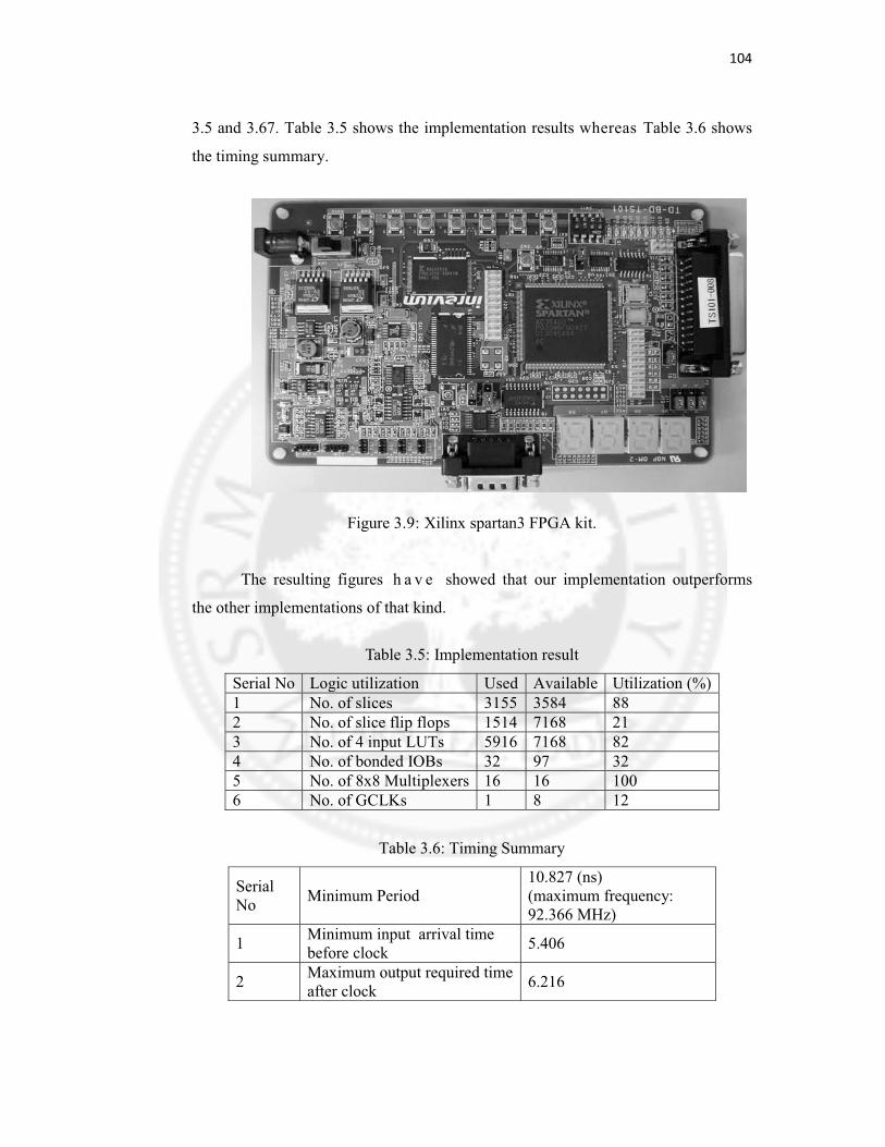
program and embedded to the VHDL code. The implementation results a f t e r
i m p l em en t i n g in Xi l inx Spar t an3 FPGA (see Figure.3.9) are listed in Table
104
3.5 and 3.67. Table 3.5 shows the implementation results whereas Table 3.6 shows
the timing summary.
Figure 3.9: Xilinx spartan3 FPGA kit.
The resulting figures h a v e showed that our implementation outperforms
the other implementations of that kind.
Table 3.5: Implementation result
Serial No Logic utilization Used Available Utilization (%)1 No. of slices 3155 3584 882 No. of slice flip flops 1514 7168 213 No. of 4 input LUTs 5916 7168 824 No. of bonded IOBs 32 97 325 No. of 8x8 Multiplexers 16 16 1006 No. of GCLKs 1 8 12
Table 3.6: Timing Summary
Serial No Minimum Period
10.827 (ns)(maximum frequency: 92.366 MHz)
1 Minimum input arrival time before clock 5.406
2 Maximum output required time after clock 6.216