Chapter 11 Frequency Response - ocw.snu.ac.kr
78
1 / 78 Chapter 11 Frequency Response 11.1 Fundamental Concepts 11.2 High-Frequency Models of Transistors 11.3 Analysis Procedure 11.4 Frequency Response of CE and CS Stages 11.5 Frequency Response of CB and CG Stages 11.6 Frequency Response of Followers 11.7 Frequency Response of Cascode Stage 11.8 Frequency Response of Differential Pairs 11.9 Additional Examples
Transcript of Chapter 11 Frequency Response - ocw.snu.ac.kr

1 / 78
Chapter 11 Frequency Response
11.1 Fundamental Concepts
11.2 High-Frequency Models of Transistors
11.3 Analysis Procedure
11.4 Frequency Response of CE and CS Stages
11.5 Frequency Response of CB and CG Stages
11.6 Frequency Response of Followers
11.7 Frequency Response of Cascode Stage
11.8 Frequency Response of Differential Pairs
11.9 Additional Examples

2 / 78
Chapter Outline
CH 11 Frequency ResponseCH 11 Frequency Response

3 / 78CH 11 Frequency ResponseCH 11 Frequency Response
High Frequency Roll-off of Amplifier
As frequency of operation increases, the gain of amplifier
decreases. This chapter analyzes this problem.
4 / 78CH 11 Frequency Response
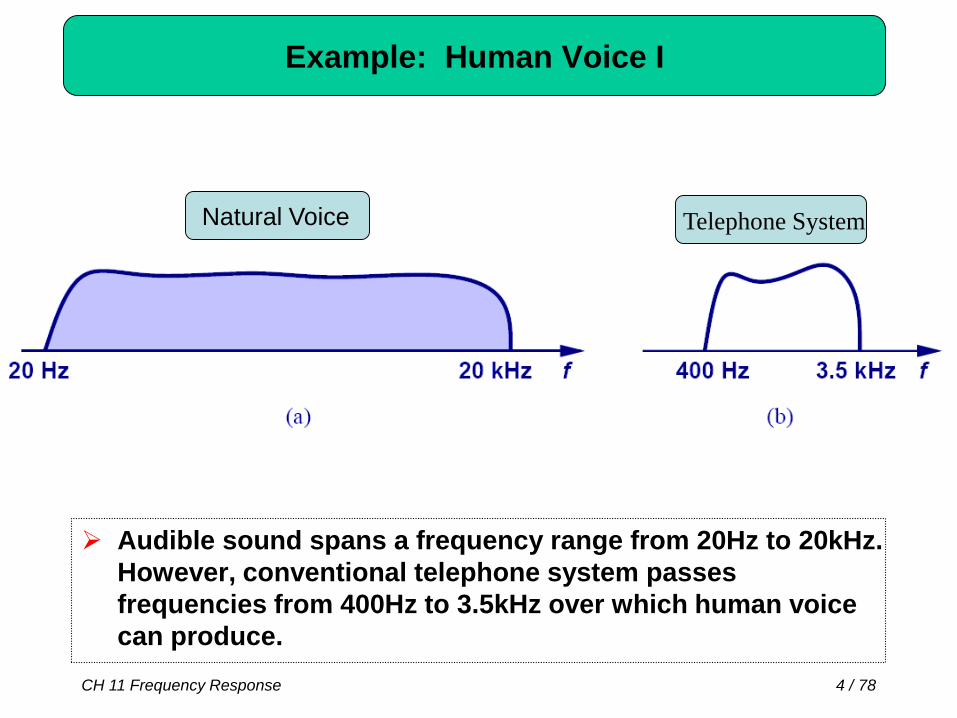
Example: Human Voice I
Audible sound spans a frequency range from 20Hz to 20kHz.
However, conventional telephone system passes
frequencies from 400Hz to 3.5kHz over which human voice
can produce.
Natural Voice Telephone System

5 / 78CH 11 Frequency Response
Example: Human Voice II
CH 11 Frequency Response
Mouth RecorderAir
Mouth EarAir
Skull
Path traveled by the human voice to the voice recorder
Path traveled by the human voice to the human ear
Since the paths are different, the results will also be
different.
6 / 78CH 11 Frequency Response
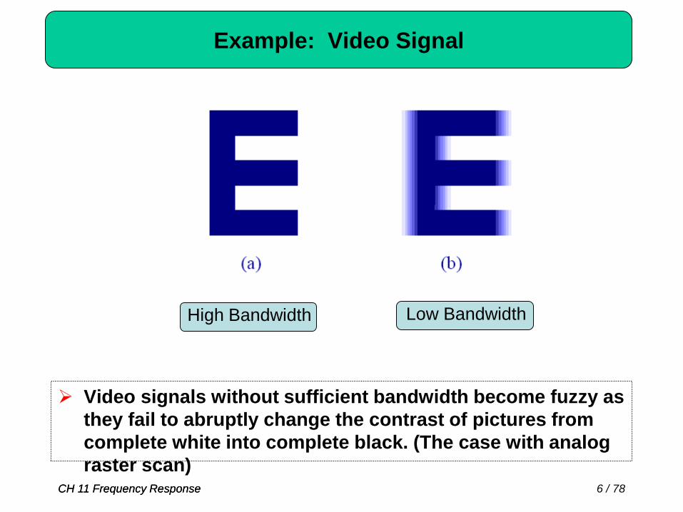
Example: Video Signal
Video signals without sufficient bandwidth become fuzzy as
they fail to abruptly change the contrast of pictures from
complete white into complete black. (The case with analog
raster scan)CH 11 Frequency Response
High Bandwidth Low Bandwidth

7 / 78CH 11 Frequency Response
Gain Roll-off: Simple Low-pass Filter
In this simple example, as frequency increases the
impedance of C1 decreases and the voltage divider consists
of C1 and R1 attenuates Vin to a greater extent at the output.
CH 11 Frequency Response
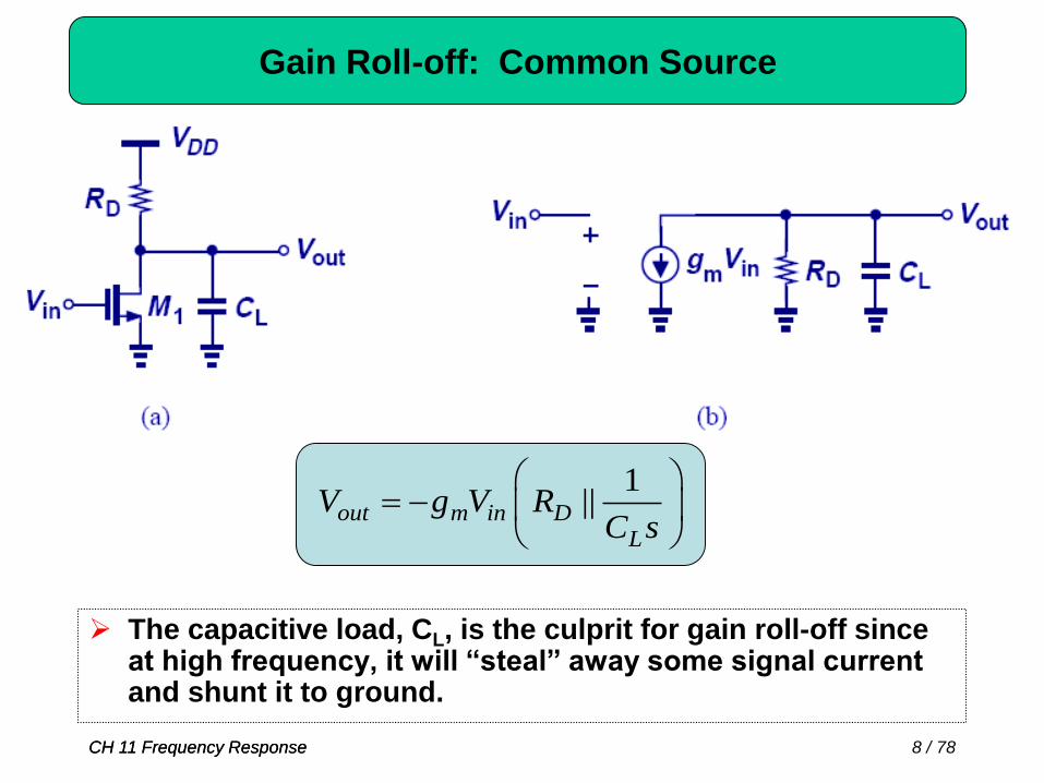
8 / 78CH 11 Frequency ResponseCH 11 Frequency Response
Gain Roll-off: Common Source
The capacitive load, CL, is the culprit for gain roll-off since at high frequency, it will “steal” away some signal current and shunt it to ground.
1||out m in D
L
V g V RC s

9 / 78CH 11 Frequency ResponseCH 11 Frequency Response
Frequency Response of the CS Stage
At low frequency, the capacitor is effectively open and the gain is flat. As frequency increases, the capacitor tends to a short and the gain starts to decrease. A special frequency is ω=1/(RDCL), where the gain drops by 3dB.
2 2 2
1
1
1
out
in
m D
L
m D
D L
out m D
in D L
VH s s
V
g RC s
g R
R C s
V g R
V R C

10 / 78CH 11 Frequency ResponseCH 11 Frequency Response
Example: Figure of Merit
This metric quantifies a circuit’s gain, bandwidth, and power
dissipation. In the bipolar case, low temperature, supply, and
load capacitance mark a superior figure of merit.
. . .
1
1
1
m C
C L
C CC
CC
T C L
C CC
T CC L
Gain BandwidthF O M
Power Consumption
g RR C
I V
IR
V R C
I V
V V C

11 / 78CH 11 Frequency Response
Example: Relationship between Frequency
Response and Step Response
CH 11 Frequency Response
2 2 21 1
1
1H s j
R C
0
1 1
1 expout
tV t V u t
R C
The relationship is such that as R1C1 increases, the
bandwidth drops and the step response becomes slower.

12 / 78CH 11 Frequency ResponseCH 11 Frequency Response
Bode Plot
When we hit a zero, ωzj, the Bode magnitude rises with a
slope of +20dB/dec.
When we hit a pole, ωpj, the Bode magnitude falls with a
slope of -20dB/dec
21
210
11
11
)(
pp
zz
ss
ss
AsH
13 / 78CH 11 Frequency ResponseCH 11 Frequency Response
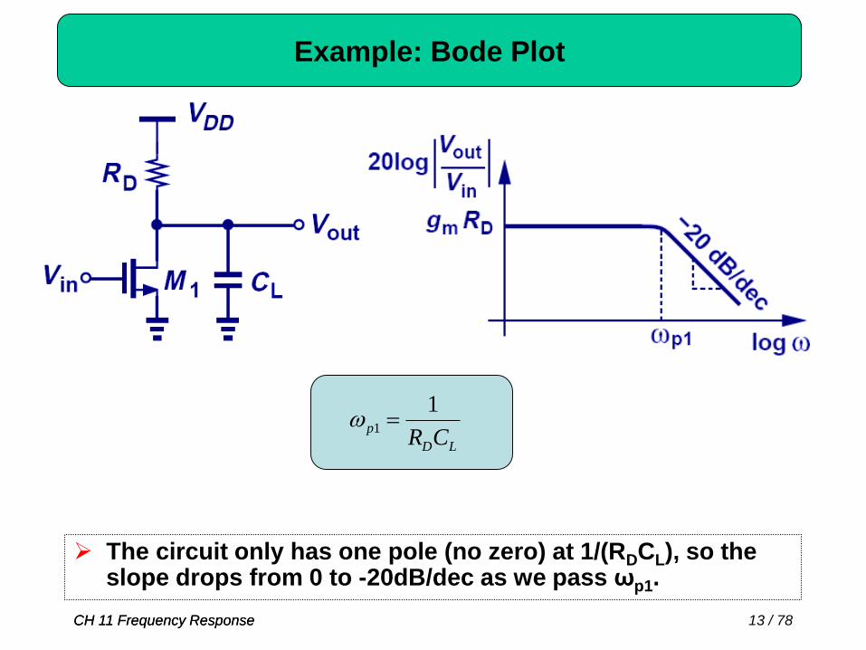
Example: Bode Plot
The circuit only has one pole (no zero) at 1/(RDCL), so the slope drops from 0 to -20dB/dec as we pass ωp1.
1
1p
D LR C

14 / 78CH 11 Frequency ResponseCH 11 Frequency Response
Pole Identification Example I
1
1p
S inR C 2
1p
D LR C
2
2
22
1
2 11 pp
Dm
in
out Rg
V
V

15 / 78CH 11 Frequency ResponseCH 11 Frequency Response
Pole Identification Example II
1
1
1||
p
S in
m
R Cg
2
1p
D LR C

16 / 78CH 11 Frequency ResponseCH 11 Frequency Response
Circuit with Floating Capacitor
The pole of a circuit is computed by finding the effective
resistance and capacitance from a node to GROUND.
The circuit above creates a problem since neither terminal
of CF is grounded.
17 / 78CH 11 Frequency ResponseCH 11 Frequency Response
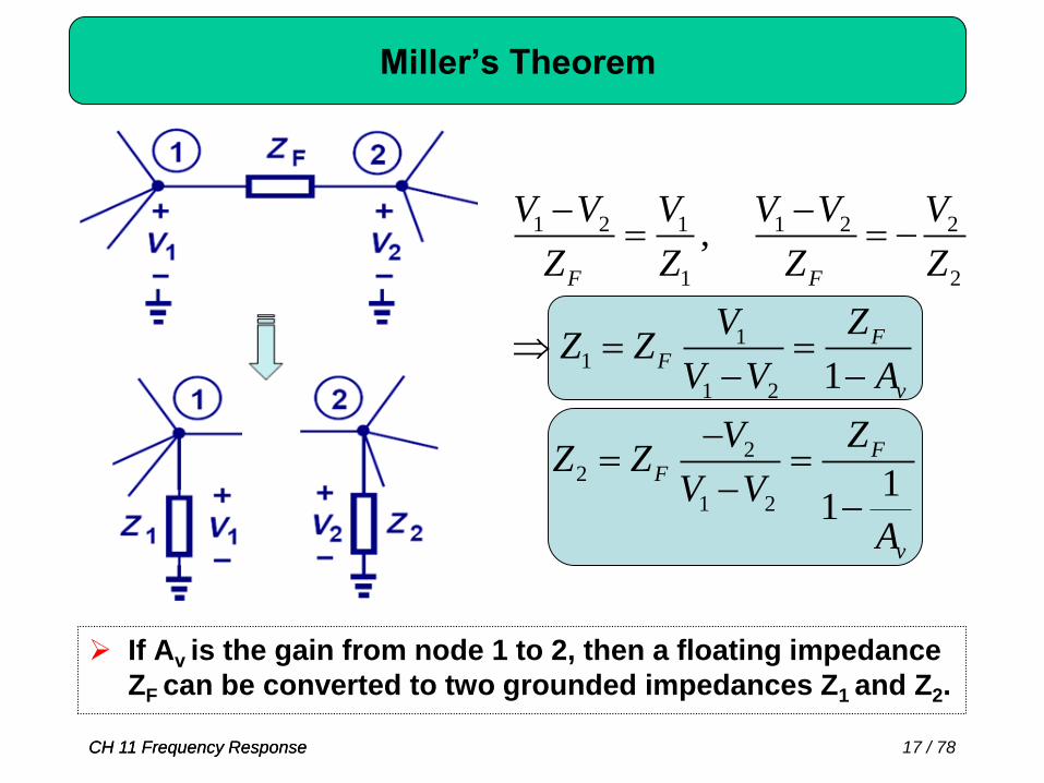
Miller’s Theorem
If Av is the gain from node 1 to 2, then a floating impedance
ZF can be converted to two grounded impedances Z1 and Z2.
1 2 1 1 2 2
1 2
11
1 2
22
1 2
,
1
1
1
F F
FF
v
FF
v
V V V V V V
Z Z Z Z
V ZZ Z
V V A
V ZZ Z
V V
A

18 / 78CH 11 Frequency ResponseCH 11 Frequency Response
Miller Multiplication
With Miller’s theorem, we can separate the floating capacitor. However, the input capacitor is larger than the original floating capacitor. We call this Miller multiplication.
1
0
1
1 1
F
v F
ZZ
A A C s
2
0
1
1 11 1
F
Fv
ZZ
C sA A
19 / 78CH 11 Frequency ResponseCH 11 Frequency Response
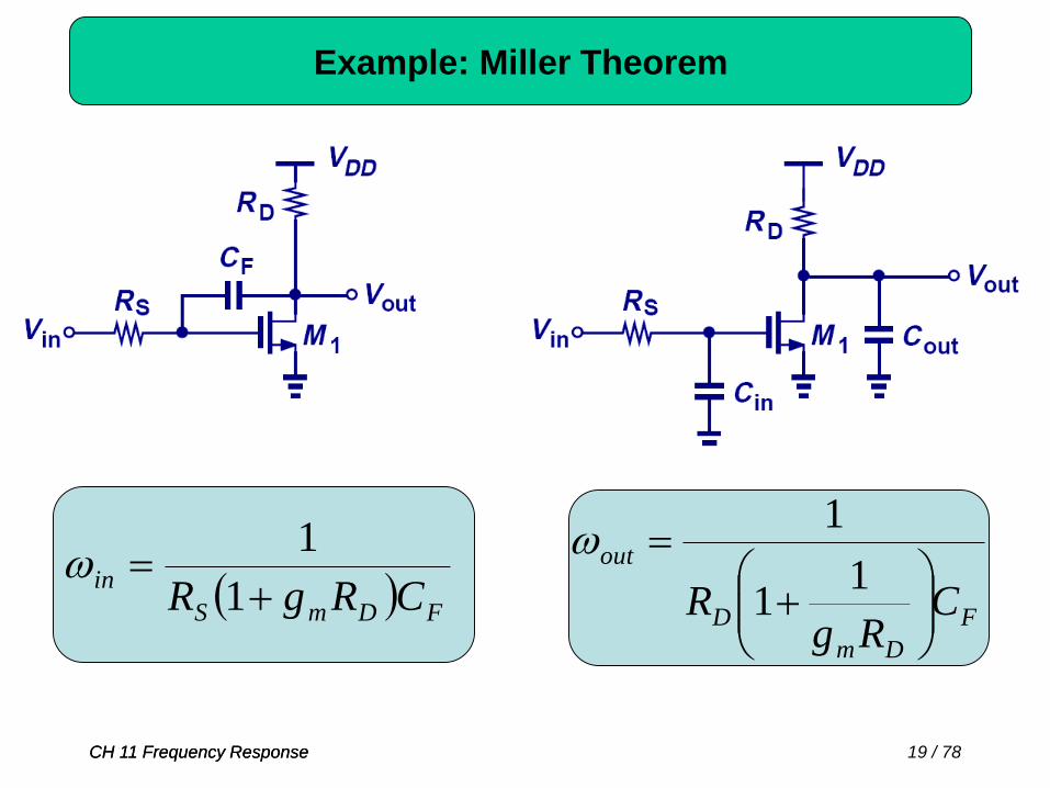
Example: Miller Theorem
FDmS
inCRgR
1
1
F
Dm
D
out
CRg
R
1
1
1

20 / 78CH 11 Frequency Response
High-Pass Filter Response
12
1
2
1
2
1
11
CR
CR
V
V
in
out
The voltage division between a resistor and a capacitor can be configured such that the gain at low frequency is reduced.
CH 11 Frequency Response
21 / 78CH 11 Frequency Response
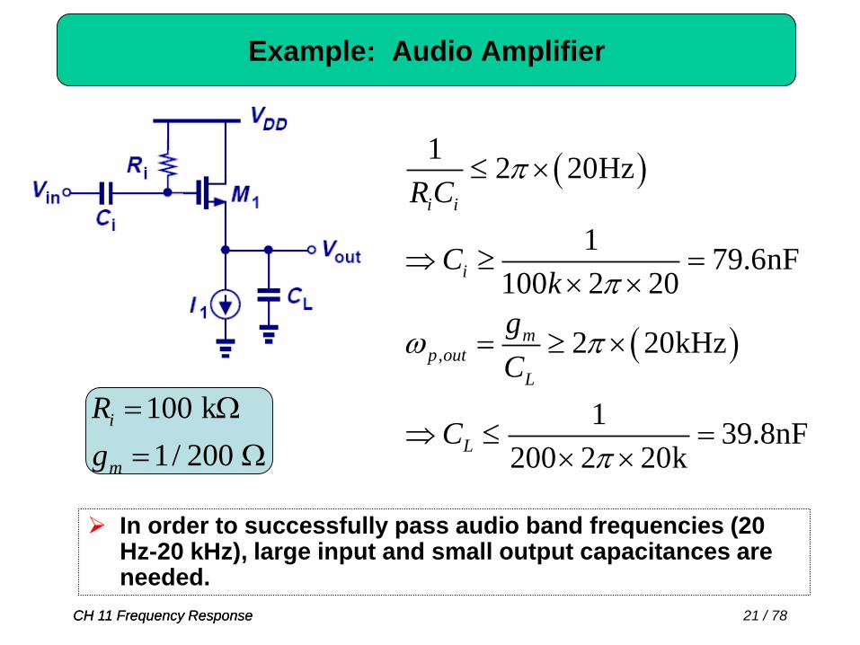
Example: Audio Amplifier
,
12 20Hz
179.6nF
100 2 20
2 20kHz
139.8nF
200 2 20k
i i
i
mp out
L
L
R C
Ck
g
C
C
In order to successfully pass audio band frequencies (20 Hz-20 kHz), large input and small output capacitances are needed.
100 k
1/ 200
i
m
R
g
CH 11 Frequency Response

22 / 78CH 11 Frequency Response
Capacitive Coupling vs. Direct Coupling
Capacitive coupling, also known as AC coupling, passes
AC signals from Y to X while blocking DC contents.
This technique allows independent bias conditions between
stages. Direct coupling does not.
Capacitive Coupling Direct Coupling
CH 11 Frequency Response

23 / 78CH 11 Frequency Response
Typical Frequency Response
Lower Corner Upper Corner
CH 11 Frequency Response

24 / 78CH 11 Frequency ResponseCH 11 Frequency Response
High-Frequency Bipolar Model
At high frequency, capacitive effects come into play. Cb
represents the base charge, whereas C and Cje are the
junction capacitances.
b jeC C C

25 / 78CH 11 Frequency ResponseCH 11 Frequency Response
High-Frequency Model of Integrated Bipolar
Transistor
Since an integrated bipolar circuit is fabricated on top of a
substrate, another junction capacitance exists between the
collector and substrate, namely CCS.

26 / 78CH 11 Frequency ResponseCH 11 Frequency Response
Example: Capacitance Identification

27 / 78CH 11 Frequency ResponseCH 11 Frequency Response
MOS Intrinsic Capacitances
For a MOS, there exist oxide capacitance from gate to channel, junction capacitances from source/drain to substrate, and overlap capacitance from gate to source/drain.

28 / 78CH 11 Frequency ResponseCH 11 Frequency Response
Gate Oxide Capacitance Partition and Full Model
The gate oxide capacitance is often partitioned between source
and drain. In saturation, C2 ~ Cgate, and C1 ~ 0. They are in
parallel with the overlap capacitance to form CGS and CGD.

29 / 78CH 11 Frequency ResponseCH 11 Frequency Response
Example: Capacitance Identification
DB1 DB2
GS2
C +C
+C

30 / 78CH 11 Frequency ResponseCH 11 Frequency Response
Transit Frequency
Transit frequency, fT, is defined as the frequency where the
current gain from input to output drops to 1.
2 2 2 2 2
1,
1 1
1 1
2
The transit frequency of MOSFETs
is obtained in a similar fashion.
2
in out m in in
out m
in
outT
in
mT T
mT T
GS
Z r I g I ZC s
I g r
I r C s r C s
Ir C
I
gf
C
gf
C

31 / 78CH 11 Frequency Response
Example: Transit Frequency Calculation
2
,
2 29 6
,1980
2
,
From Problem 11.28,
32
2
100 40059
65 10 1 10
If 400 / ,
226
nT GS TH
T today
T s
n
T today
f V VL
f
f
cm V s
f GHz
CH 11 Frequency Response
The minimum channel length of MOSFETs has been scaled
from 1μm in the late 1980s to 65nm today. Also, the
inevitable reduction of the supply voltage has reduced the
gate-source overdrive voltage from about 400mV to 100mV.
By what factor has the fT of MOSFETs increased?

32 / 78CH 11 Frequency Response
Analysis Summary
The frequency response refers to the magnitude of the
transfer function.
Bode’s approximation simplifies the plotting of the
frequency response if poles and zeros are known.
In general, it is possible to associate a pole with each node
in the signal path.
Miller’s theorem helps to decompose floating capacitors
into grounded elements.
Bipolar and MOS devices exhibit various capacitances that
limit the speed of circuits.
CH 11 Frequency Response

33 / 78CH 11 Frequency Response
High Frequency Circuit Analysis Procedure
Determine which capacitor impact the low-frequency region
of the response and calculate the low-frequency pole
(neglect transistor capacitance).
Calculate the midband gain by replacing the capacitors with
short circuits (neglect transistor capacitance).
Include transistor capacitances.
Merge capacitors connected to AC grounds and omit those
that play no role in the circuit.
Determine the high-frequency poles and zeros.
Plot the frequency response using Bode’s rules or exact
analysis.
CH 11 Frequency Response

34 / 78CH 11 Frequency Response
Frequency Response of CS Stage
Ci acts as a high pass filter.
Lower cut-off frequency must be lower than the lowest
signal frequency fsig,min (20 Hz in audio applications).
CH 11 Frequency Response
1 21 2
1 21 2
1 1
iX
in i
i
R R C sR RVs
V R R C sR R
C s
,min
1 2
1
2sig
i
fR R C
Thus,

35 / 78CH 11 Frequency Response
Frequency Response of CS Stage
with Bypassed Degeneration
1
1 1 1
m D S bout D
X S b m SS
b m
g R R C sV Rs
V R C s g RR
C s g
In order to increase the midband gain, a capacitor Cb is
placed in parallel with Rs.
The pole frequency must be well below the lowest signal
frequency to avoid the effect of degeneration.
CH 11 Frequency Response
1
out D
XS
m
V Rs
VR
g

36 / 78CH 11 Frequency ResponseCH 11 Frequency Response
Unified Model for CE and CS Stages

37 / 78CH 11 Frequency ResponseCH 11 Frequency Response
Unified Model Using Miller’s Theorem
,
1
1p in
Thev in m L XYR C g R C
,
1
11
p out
L out XY
m L
R C Cg R
r

38 / 78CH 11 Frequency Response
Example: CE Stage
p,in
p,out
2 516 MHz
2 1.59 GHz
(a) Calculate the input and output poles if RL=2 kΩ. Which
node appears as the speed bottleneck?
CH 11 Frequency Response
,
1
1p in
S m LR r C g R C
,
1
11
p out
L CS
m L
R C Cg R
200 , 1 mA
100, 100 fF
20 fF, 30 fF
S C
CS
R I
C
C C

39 / 78CH 11 Frequency Response
Example: CE Stage – cont’d
(b) Is it possible to choose RL such that the output pole
limits the bandwidth?
, ,
m L
1 1
1 11
If g R 1,
p in p out
S m L
L CS
m L
CS m S L S
R r C g R CR C C
g R
C C g R r C R R r C
With the values assumed in this example, the left-hand side is negative,
implying that no solution exists. Thus, the input pole remains the speed
bottleneck.

40 / 78CH 11 Frequency Response
Example: Half Width CS Stage
W 2X
bias current 2X
2
21
2
1
221
2
1
,
,
XY
Lm
outL
outp
XYLminS
inp
C
Rg
CR
CRgCR
CH 11 Frequency Response
m n ox D
Wg 2 C I 2X
L
capacitances 2X
bandwidth 2X
gain 2X
gain bandwidth constant

41 / 78CH 11 Frequency Response
Direct Analysis of CE and CS Stages
1
1At Node Y:
XY out
LX out XY m X out out X out
L XY m
C s C sR
V V C s g V V C s V VR C s g
2 1
XY m Lout
Thev
C s g RVs
V as bs
At Node X: X Thevout X XY X in
Thev
V VV V C s V C s
R
1
1XY out
ThevLout XY XY in out
Thev XY m Thev
C s C sVR
V C s C s C s VR C s g R
where ,
1
Thev L in XY out XY in out
m L XY Thev Thev in L XY out
a R R C C C C C C
b g R C R R C R C C

42 / 78CH 11 Frequency ResponseCH 11 Frequency Response
Direct Analysis of CE and CS Stages – cont’d
Direct analysis yields different pole locations and an extra zero.
22
1 2 1 2 1 2
1 1 1
2 1 p1 p2 p1
1
1
2
| |
1 11 1 1 1
1
1
1
1| |
mz
XY
p p p p p p
p p
p
p
m L XY Thev Thev in L XY out
m L XY Thev Thev in L XY o
p
g
C
s s sas bs s
if
b
g R C R R C R C C
g R C R R C R C Cb
a
ut
Thev L in XY out XY in outR R C C C C C C
Dominant-pole approximation

43 / 78CH 11 Frequency ResponseCH 11 Frequency Response
Example: Dominant-pole approximation
outinXYoutXYinOOS
outXYOOinSSXYOOmp
outXYOOinSSXYOOm
p
CCCCCCrrR
CCrrCRRCrrg
CCrrCRRCrrg
21
212112
21211
1
||
)(||||1
)(||||1
1
1
1
1 2 2
in GS
XY GD
out DB GD DB
C C
C C
C C C C

44 / 78CH 11 Frequency Response
Example: Comparison Between Different Methods
,
,
2 571 MHz
2 428 MHz
p in
p out
2 264 MHz
2 4 53 GHz
p,in
p ,out .
2 249 MHz
2 4 79 GHz
p,in
p ,out .
1
200
250 fF
80 fF
100fF
150
0
2 k
S
GS
GD
DB
m
L
R
C
C
C
g
R
Miller’s Exact Dominant Pole
This error arises because we have multiplied by the midband
gain (1+ ) rather than the gain at high frequencies.
GD
m L
C
g R

45 / 78CH 11 Frequency ResponseCH 11 Frequency Response
Input Impedance of CE and CS Stages
rsCRgC
ZCm
in ||1
1
sCRgCZ
GDDmGS
in
1
1

46 / 78CH 11 Frequency Response
Low Frequency Response of CB and CG Stages
out C m C i
1
in m S i mS i m
V R g R C ss
V 1 g R C s gR C s 1/ g
As with CE and CS stages, the use of capacitive coupling
leads to low-frequency roll-off in CB and CG stages
(although a CB stage is shown above, a CG stage is similar).
CH 11 Frequency Response

47 / 78CH 11 Frequency ResponseCH 11 Frequency Response
Frequency Response of CB Stage
X
m
S
Xp
Cg
R
1||
1,
CCX
,
1p Y
C YR C
CSY CCC
Or

48 / 78CH 11 Frequency ResponseCH 11 Frequency Response
Frequency Response of CG Stage
Or
X
m
S
Xp
Cg
R
1||
1,
SBGSX CCC
,
1p Y
D YR C
DBGDY CCC
Similar to a CB stage, the input pole is on the order of fT, so
rarely a speed bottleneck.
Or

49 / 78CH 11 Frequency ResponseCH 11 Frequency Response
Example: CG Stage Pole Identification
p,X
S SB1 GS1
m1
1
1R || C C
g
2211
2
, 1
1
DBGSGDDB
m
Yp
CCCCg

50 / 78CH 11 Frequency Response
Example: Frequency Response of CG Stage
1
200
250 fF
80 fF
100 fF
150
0
2 kΩ
S
GS
GD
DB
m
D
R
C
C
C
g
R
,
,
11/ || 2 5.31 GHz
/ 2 442 MHz
p X S X
m
p Y L Y
R Cg
R C

51 / 78CH 11 Frequency ResponseCH 11 Frequency Response
Emitter and Source Followers
The following will discuss the frequency response of
emitter and source followers using direct analysis.
Emitter follower is treated first and source follower is
derived easily by allowing r to go to infinity.

52 / 78CH 11 Frequency ResponseCH 11 Frequency Response
Direct Analysis of Emitter Follower
1
2
1
with 1
out mm
in
Cs
V gr g
V as bs
At node X: 0out inout
S
V V V VV V C s V C s
R r
At output node: 1
out Lm out L
m
V V C sV C s g V V C s V
rC s g
r
mz T
gf
C
where
1
SL L
m
S LS
m m
Ra C C C C C C
g
C R Cb R C
g r g
53 / 78CH 11 Frequency ResponseCH 11 Frequency Response
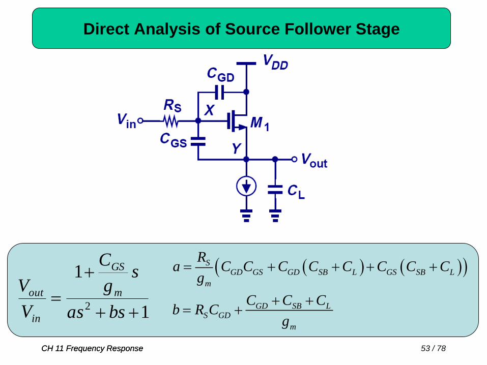
Direct Analysis of Source Follower Stage
1
1
2
bsas
sg
C
V
V m
GS
in
out
SGD GS GD SB L GS SB L
m
GD SB LS GD
m
Ra C C C C C C C C
g
C C Cb R C
g

54 / 78CH 11 Frequency Response
Example: Frequency Response of Source Follower
1
200
100 fF
250 fF
80 fF
100 fF
150
0
S
L
GS
GD
DB
m
R
C
C
C
C
g
21 2
11
1
2
2.58 10
5.8 10
/ 2 4.24 GHz
2 1.79 GHz 2.57 GHz
2 1.79 GHz 2.57 GHz
z m GS
p
p
a s
b s
g C
j
j

55 / 78CH 11 Frequency ResponseCH 11 Frequency Response
Example: Source Follower
1
1
2
bsas
sg
C
V
V m
GS
in
out
1
22111
2211111
1
))((
m
DBGDSBGDGDS
DBGDSBGSGDGSGD
m
S
g
CCCCCRb
CCCCCCCg
Ra

56 / 78CH 11 Frequency ResponseCH 11 Frequency Response
Input Capacitance of Emitter/Source Follower
1 1
1 1
1
Lv X v XY XY
m LL
m
XYin GD
m L
RA C A C C
g RR
g
CC C or C
g R

57 / 78CH 11 Frequency ResponseCH 11 Frequency Response
Example: Source Follower Input Capacitance
1 2
1 2
1
1 1
1 1
1 1 2
1
1
1
1 ||
O O
v
O O
m
in GD v GS
GD GS
m O O
r rA
r rg
C C A C
C Cg r r

58 / 78CH 11 Frequency ResponseCH 11 Frequency Response
Output Impedance of Emitter Follower
1
X m S X
S SX
X
I g V R V V
R r C s r RV
I r C s
1
1
X m
X
I g V r VC s
rV I
r C s

59 / 78CH 11 Frequency ResponseCH 11 Frequency Response
Output Impedance of Source Follower
1
with
1
S SX
X
m
S GSX
X GS m
R r C s r RV
I r C s
g r
R C sV
I C s g
60 / 78CH 11 Frequency ResponseCH 11 Frequency Response
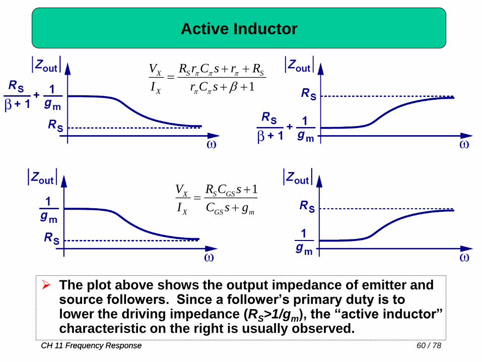
Active Inductor
The plot above shows the output impedance of emitter and source followers. Since a follower’s primary duty is to lower the driving impedance (RS>1/gm), the “active inductor” characteristic on the right is usually observed.
1
S SX
X
R r C s r RV
I r C s
1S GSX
X GS m
R C sV
I C s g

61 / 78CH 11 Frequency ResponseCH 11 Frequency Response
Example: Output Impedance
33
321 1||
mGS
GSOO
X
X
gsC
sCrr
I
V
O3r

62 / 78CH 11 Frequency ResponseCH 11 Frequency Response
Frequency Response of Cascode Stage
For cascode stages, there are three poles and Miller
multiplication is smaller than in the CE/CS stage.
Assuming for all transistors,or
,1
2
x v XY XY
XY
C A C
C
1,
2
1mv XY
m
gA
g

63 / 78CH 11 Frequency ResponseCH 11 Frequency Response
Poles of Bipolar Cascode
111
,2||
1
CCrRS
Xp
121
2
,
21
1
CCCg
CS
m
Yp
22
,
1
CCR CSL
outp
64 / 78CH 11 Frequency ResponseCH 11 Frequency Response
Poles of MOS Cascode
1
2
11
,
1
1
GD
m
mGSS
Xp
Cg
gCR
1
1
221
2
,
11
1
GD
m
mGSDB
m
Yp
Cg
gCC
g
22
,
1
GDDBL
outpCCR

65 / 78CH 11 Frequency Response
Example: Frequency Response of Cascode
1
200
250 fF
80 fF
100 fF
150
0
2 kΩ
S
GS
GD
DB
m
L
R
C
C
C
g
R
,
,
,
2 1.95 GHz
2 1.73 GHz
2 442 MHz
p X
p Y
p out

66 / 78CH 11 Frequency ResponseCH 11 Frequency Response
MOS Cascode Example
1
2
11
,
1
1
GD
m
mGSS
Xp
Cg
gCR
,
21 2 1 2 3 3
2 1
1
11
p Y
mDB GS GD SB GD DB
m m
gC C C C C C
g g
22
,
1
GDDBL
outpCCR

67 / 78CH 11 Frequency ResponseCH 11 Frequency Response
I/O Impedance of Bipolar Cascode
sCCrZ in
11
12
1||
sCC
RZCS
Lout
22
1||

68 / 78CH 11 Frequency ResponseCH 11 Frequency Response
I/O Impedance of MOS Cascode
sCg
gC
Z
GD
m
mGS
in
1
2
11 1
1
sCCRZ
DBGD
Lout
22
1||

69 / 78CH 11 Frequency ResponseCH 11 Frequency Response
Bipolar Differential Pair Frequency Response
Since bipolar differential pair can be analyzed using half-circuit, its transfer function, I/O impedances, locations of poles/zeros are the same as that of the half circuit’s.
Half Circuit

70 / 78CH 11 Frequency ResponseCH 11 Frequency Response
MOS Differential Pair Frequency Response
Since MOS differential pair can be analyzed using half-circuit, its transfer function, I/O impedances, locations of poles/zeros are the same as that of the half circuit’s.
Half Circuit

71 / 78CH 11 Frequency ResponseCH 11 Frequency Response
Example: MOS Differential Pair
,
1 1 3 1
,
31 3 3 1
3 1
,
3 3
1
[ (1 / ) ]
1
11
1
p X
S GS m m GD
p Y
mDB GS SB GD
m m
p out
L DB GD
R C g g C
gC C C C
g g
R C C

72 / 78CH 11 Frequency Response
Common Mode Frequency Response
1
2 11 12
m D SS SSout D
CM SS SS m SS
SS
m SS
g R R C sV R
V R C s g RR
g C s
Css will lower the total impedance between point P to ground at high frequency, leading to higher CM gain which degrades the CM rejection ratio.

73 / 78CH 11 Frequency Response
Tail Node Capacitance Contribution
Source-Body Capacitance of M1, M2
Drain-Body Capacitance of M3
Gate-Drain Capacitance of M3
CH 11 Frequency Response

74 / 78CH 11 Frequency Response
Example: Capacitive Coupling
1 1
11
1
1 1 1
1
1 1
1
For , assuming 800 mV,
1.7 mA
ln / 748 mV
1.75 mA 14.9
1.49 k
BE
CC BEC
B
BE T C S
C m
Q V
V VI
R
V V I I
I g
r
2 2
2 2 2 2
22
2
1
2 2
2
For Q , assuming 800mV,
1.13 mA/
Iteration yields
1.17 mA, 22.2
2.22 k
BE
CC B B BE E C
CC BEC
B E
C m
V
V I R V R I
V VI
R R
I g
r
165 10 A
100
S
A
I
V
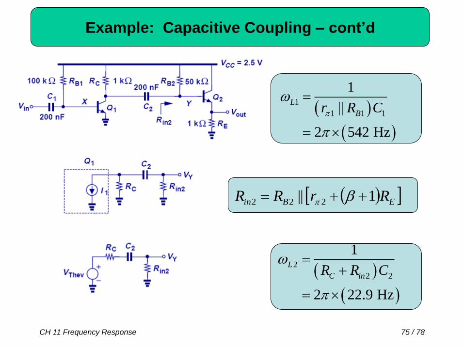
75 / 78CH 11 Frequency Response
Example: Capacitive Coupling – cont’d
EBin RrRR 1|| 222
2
2 2
1
2 22.9 Hz
L
C inR R C
1
1 1 1
1
||
2 542 Hz
L
Br R C
76 / 78CH 11 Frequency Response
2
1 2 2
1
2 6.92 MHz
L
D inR R C
1
1 1
1
1 1
1 1
1
1
1
2 42.4 MHz
L
S
m
m S
S
R Cg
g R
R C
2
2
2 2 2
2
1
6.67
1.30 k
Fin
v
v m D
in
RR
A
A g R
R
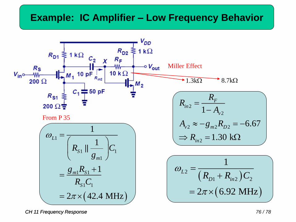
Example: IC Amplifier – Low Frequency Behavior
CH 11 Frequency Response
From P 35
Miller Effect
1.3k 8.7k

77 / 78CH 11 Frequency Response
1 1 2
2 2
|| 3.77
6.67
25.1
out outX
in in X
Xm D in
in
outm D
X
out
in
v vv
v v v
vg R R
v
vg R
v
v
v
Example: IC Amplifier – Midband Behavior

78 / 78CH 11 Frequency Response
Example: IC Amplifier – High Frequency Behavior
1
v2 GD2 GD2
With Miller effect,
1 A C 1.15 C
1
2
2 (308 MHz)
2 (2.15 GHz)
p
p
3
2 2 2
1
(1.15 )
2 (1.21GHz)
p
L GD DBR C C
28dB
42.4 MHz
308 MHz6.92 MHz
1.21 GHz
2.15 GHz