Frequency dependent dynamical electromechanical response ... · Frequency dependent dynamical...
15
Frequency dependent dynamical electromechanical response of mixed ionic-electronic conductors A. N. Morozovska, E. A. Eliseev, S. L. Bravina, Francesco Ciucci, G. S. Svechnikov et al. Citation: J. Appl. Phys. 111, 014107 (2012); doi: 10.1063/1.3673868 View online: http://dx.doi.org/10.1063/1.3673868 View Table of Contents: http://jap.aip.org/resource/1/JAPIAU/v111/i1 Published by the American Institute of Physics. Related Articles Sodium ionic conduction in complex hydrides with [BH4]− and [NH2]− anions Appl. Phys. Lett. 100, 203904 (2012) Defect chemistry of Ti-doped antiferroelectric Bi0.85Nd0.15FeO3 Appl. Phys. Lett. 100, 182902 (2012) Fundamentals of ionic conductivity relaxation gained from study of procaine hydrochloride and procainamide hydrochloride at ambient and elevated pressure J. Chem. Phys. 136, 164507 (2012) Structure and ion transport in Li3Fe2(PO4)3 synthesized by solution combustion technique J. Appl. Phys. 111, 064905 (2012) Ion assisted growth of B4C diffusion barrier layers in Mo/Si multilayered structures J. Appl. Phys. 111, 064303 (2012) Additional information on J. Appl. Phys. Journal Homepage: http://jap.aip.org/ Journal Information: http://jap.aip.org/about/about_the_journal Top downloads: http://jap.aip.org/features/most_downloaded Information for Authors: http://jap.aip.org/authors Downloaded 31 May 2012 to 146.186.211.55. Redistribution subject to AIP license or copyright; see http://jap.aip.org/about/rights_and_permissions
Transcript of Frequency dependent dynamical electromechanical response ... · Frequency dependent dynamical...

Frequency dependent dynamical electromechanical response of mixedionic-electronic conductorsA. N. Morozovska, E. A. Eliseev, S. L. Bravina, Francesco Ciucci, G. S. Svechnikov et al. Citation: J. Appl. Phys. 111, 014107 (2012); doi: 10.1063/1.3673868 View online: http://dx.doi.org/10.1063/1.3673868 View Table of Contents: http://jap.aip.org/resource/1/JAPIAU/v111/i1 Published by the American Institute of Physics. Related ArticlesSodium ionic conduction in complex hydrides with [BH4]− and [NH2]− anions Appl. Phys. Lett. 100, 203904 (2012) Defect chemistry of Ti-doped antiferroelectric Bi0.85Nd0.15FeO3 Appl. Phys. Lett. 100, 182902 (2012) Fundamentals of ionic conductivity relaxation gained from study of procaine hydrochloride and procainamidehydrochloride at ambient and elevated pressure J. Chem. Phys. 136, 164507 (2012) Structure and ion transport in Li3Fe2(PO4)3 synthesized by solution combustion technique J. Appl. Phys. 111, 064905 (2012) Ion assisted growth of B4C diffusion barrier layers in Mo/Si multilayered structures J. Appl. Phys. 111, 064303 (2012) Additional information on J. Appl. Phys.Journal Homepage: http://jap.aip.org/ Journal Information: http://jap.aip.org/about/about_the_journal Top downloads: http://jap.aip.org/features/most_downloaded Information for Authors: http://jap.aip.org/authors
Downloaded 31 May 2012 to 146.186.211.55. Redistribution subject to AIP license or copyright; see http://jap.aip.org/about/rights_and_permissions
Frequency dependent dynamical electromechanical responseof mixed ionic-electronic conductors
A. N. Morozovska,1,a) E. A. Eliseev,1,2 S. L. Bravina,3 Francesco Ciucci,4,b)
G. S. Svechnikov,1 Long-Qing Chen,5 and S. V. Kalinin6
1Institute of Semiconductor Physics, National Academy of Science of Ukraine, 41, pr. Nauki,03028 Kiev, Ukraine2Institute for Problems of Materials Science, National Academy of Science of Ukraine, 3, Krjijanovskogo,03142 Kiev, Ukraine3Institute of Physics, National Academy of Science of Ukraine, 46, pr. Nauki, 03028 Kiev, Ukraine4The Hong Kong University of Science and Technology, Department of Mechanical Engineering,Department of Chemical and Biomolecular Engineering, Clear Water Bay, Kowloon, Hong Kong5Department of Materials Science and Engineering, Pennsylvania State University, University Park,Pennsylvania 16802, USA6The Center for Nanophase Materials Sciences, Oak Ridge National Laboratory, Oak Ridge,Tennessee 37922, USA
(Received 11 August 2011; accepted 6 December 2011; published online 9 January 2012)
Frequency dependent dynamic electromechanical response of the mixed ionic-electronic conductor film to a
periodic electric bias is analyzed for different electronic and ionic boundary conditions. Dynamic effects of
mobile ions concentration (stoichiometry contribution), charge state of acceptors (donors), electron
concentration (electron-phonon coupling via the deformation potential), and flexoelectric effect
contribution are discussed. A variety of possible nonlinear dynamic electromechanical responses of
mixed electronic ionic conductors (MIEC) films including quasi-elliptic curves, asymmetric
hysteresis-like loops with pronounced memory window, and butterfly-like curves are calculated.
The electromechanical response of ionic semiconductor is predicted to be a powerful descriptor of
local valence states, band structure and electron-phonon correlations that can be readily measured
in the nanoscale volumes and in the presence of strong electronic conductivity. VC 2012 AmericanInstitute of Physics. [doi:10.1063/1.3673868]
I. INTRODUCTION
Materials with dual electronic and ionic conductivity,
referred to as mixed electronic ionic conductors (MIECs) are
broadly used in energy related applications such as bat-
teries,1,2 sensors,3,4 and fuel cells,5,6 as well as electronic de-
vice applications including memristive, and electroresistive
memory and logic devices.7,8 Beyond these applications,
ionic and electrochemical effects can heavily contribute to
the operation of ferroelectric devices9,10 and capacitors,
including ferroelectric fatigue,9,10 ferroelectric resistive
switching,11 ferroelectric gate devices,12 or spurious observa-
tions of ferroelectricity in centrosymmetric materials in
bulk13 or SPM geometries,14–16 piezoresistive phenomena,17
and exotic memory and transport effects in nano- and molec-
ular electronic devices.18 Recently, ionic phenomena are con-
sidered as an origin of unique properties of LaAlO3-SrTiO3
interfaces.19 Many oxides such as manganites, cobaltite, and
ferrites, are both extensively studied in the condensed matter
physics community20,21 and are used in energy applications,
pointing at the possible role of ionic phenomena in classical
physical studies. The multitude of ionic phenomena in nano-
scale systems necessitates the development of comprehensive
measurement strategies applicable for nanoscale materials in
the form of capacitor-like device structure and scanning
probe microscopy (SPM).
Understanding of physical and electrochemical phenomena
in these materials necessitates development of measurement
techniques addressing local valence states and electrochemical
functionality and their response to external bias and chemical
stimuli on the local scale. Significant progress in this direction
has been achieved with the advent of electron-microscopy
based electron energy loss spectroscopy (EELS) imaging22 and
synchrotron based X-ray measurements. However, the under-
standing of these systems can be considerably extended if these
studies can be extended to local probing of functionality on a
single grain, defect, or domain wall level, combining the broad
spectrum of capabilities of conventional electrochemical char-
acterization techniques and high spatial resolution of electron
and scanning probe microscopies.
The applicability of traditional electrochemical meas-
urements based on the Faradaic current detection is necessar-
ily restricted to the 1–50 micron length scale due to the
electronic current detection limits.23,24 The comprehensive
analysis25 of recent efforts in extending the electrochemical
charge-discharge26–29 or impedance spectroscopy30–32 meth-
ods to SPM environment suggests that these studies are pos-
sible only when the process is catalyzed at and around the tip
surface junction.33 At the same time, when tip or surface
a)Author to whom correspondence should be addressed. Electronic mail:
[email protected])Electronic mail: [email protected].
0021-8979/2012/111(1)/014107/14/$30.00 VC 2012 American Institute of Physics111, 014107-1
JOURNAL OF APPLIED PHYSICS 111, 014107 (2012)
Downloaded 31 May 2012 to 146.186.211.55. Redistribution subject to AIP license or copyright; see http://jap.aip.org/about/rights_and_permissions
material are active part of the ionic or electrochemical pro-
cess, corresponding current cannot be probed directly and
the progression of reaction can be ascertained only through
static changes in surface topography, Raman signature, etc.
(e.g., for tip-induced nanooxidation,34,35 or deposition of car-
bon,36 semiconductors37 or metals38,39). This limitation
stems both from the smallness of Faradaic currents and pres-
ence of surface leakage currents (dc detection) and stray
capacitances of the measurement circuits (ac detection).
An alternative approach for probing ionic and electro-
chemical processes in solids is based on electromechanical
and chemo-mechanical coupling. The latter corresponds to
chemical expansivity measurements of volume versus chemi-
cal potential of volatile component using macroscopic dilato-
metric test systems or scattering methods, and is now broadly
used in solid state ionic community. In electromechanical
methods, potential induced by mechanical stimuli applied to
MIEC (direct effect) or mechanical response induced by elec-
trical stimuli (inverse effect) is detected. In particular, this
approach offers the advantage of direct implementation in
capacitor-like structures with interferrometric or vibrometric
detection of associated surface displacements, or implementa-
tion in the SPM setup. An example of this approach is electro-
chemical strain microscopy (ESM),40,41 in which the
periodically biased conductive SPM tip concentrates electric
field in a small volume of the material, resulting in redistribu-
tion of mobile ions through diffusion and electromigration
mechanisms. The associated changes in molar volume and
strains result into periodic surface displacement detected by a
SPM tip, somewhat similar to the piezoresponse force micros-
copy (PFM) of piezoelectric and ferroelectric materials.42–46
In systems with large background conductivity, the bias-
induced electromechanical process can be separated into the
interfacial reaction process and subsequent diffusion of the
chemical species through the lattice. This problem then
reduces to the solution of linear diffusion or coupled
diffusion-strain equations, and is well developed in the con-
text of electrochemical storage and metallurgical
systems.47–52 However, in MIEC systems, the response will
be determined by coupled ionic and electronic motion, giv-
ing rise to significantly more complex coupled diffusion-
migration problem.
To the best of our knowledge the dynamical local elec-
tromechanical properties of MIECs is poorly studied theo-
retically,23,24,40,53,54 in contrast to the theory of their
dynamical current-voltage response, that is well elaborated
(see, e.g., classical papers of Riess et al.7,8 and Strukov
et al.55 and references therein). The basis of theory of static
local electromechanical properties of MIECs is presented
in Ref. 56.
The paper is organized as follows: The electromechani-
cal and transport phenomena in MIECs are summarized in
Sec. II. Section III contains basic equations and boundary
conditions for dynamic local electromechanical response cal-
culations. Results of the dynamic response calculations are
presented and analyzed in Sec. IV. The linear response is an-
alyzed in Sec. IV A. Nonlinearity effect on the response is
analyzed in Secs. IV B 3. These sections are followed by the
brief discussion and summary remarks in Sec. V.
II. ELECTROMECHANICAL AND TRANSPORTPHENOMENA IN MIECs
A. Electromechanical coupling in MIECs
Electromechanical coupling in MIECs is controlled by
relationships between molar volume and local field, carrier
concentration, and ionic concentration. Well-known effect of
the stoichiometry on the local strain is the (often linear) de-
pendence of lattice constants on the composition of solid so-
lution (Vegard law of chemical expansion). The deviations
from Vegard law are typically indicative of non–trivial phys-
ical phenomena including phase separation, metal insulator
transitions, and thus are intrinsically linked to the fundamen-
tal physics of the material. Recent experimental studies of
correlated oxides including ceria, titanates, ferrites, cobal-
tites, nikelates analyze chemical expansion effects as related
to the oxygen vacancies appearance and migration. Adler etal.57–59 analyzed the temperature and oxidation–
state dependence of lattice volume in La1–xSrxCoyFe1�yO3–d
ceramics in terms of thermal and chemical expansion. A sim-
ilar effect of lattice expansion due to the oxygen non-
stoichiometry was observed earlier by the different authors
(see, e.g., Refs. 60–62). Bishop et al.63 studied the chemical
expansion and oxygen non-stoichiometry of undoped and
Gd-doped cerium oxide exposed to different partial pressures
of oxygen and found that the contribution to a chemical
expansion could be attributed to the larger crystal radius of
cerium Ce3þ compared to the cerium Ce4þ. Phenomenologi-
cal models accounting for the difference in the dopant cation
radius and charge as well as the formation of oxygen vacan-
cies have been used to explain experimental results for
fluorite-structure oxides64,65 assuming linear relations resem-
bling Vegard law. Lankhorst et al.66 established the
relationship between defect chemistry, oxygen nonstoichi-
ometry, and electronic properties (i.e., Fermi level position)
in MIEC La1�xSrxCoO3�d.
The second effect leading to electromechanical coupling
in oxides are the electron-phonon coupling via deformation
potential.56,67 Strong electron-phonon coupling associated
with the local Jahn-Teller distortion was proposed as a possi-
ble origin of this very unusual behavior of materials with
transition-metal ions.20 Coupling between orbital occupancy
and the Jahn-Teller distortion can play a major role as a driv-
ing force of symmetry breaking, because the orbital occupa-
tion may strongly couple to the lattice (anion distortion) in
some cases.20 Jahn-Teller distortions are typical for correlated
oxides with partially filled d-orbitals (e.g., t2 g and eg for octa-
hedral and tetrahedral coordinates) such as
La1�xSrxMnO3�d,68 La1�xSrxCoO3�d and even SrFexTi1�x
O3�d.69 The bandgap of La1�xSrxMnO3�d (�1 eV) is mainly
determined by the collective Jahn-Teller distortion.70 Since
the deformation potential is directly related with the bandgap
in the narrow gap semiconductors, Fermi level in (half) metals
as well as with the charge gap in correlated metal-insula-
tors,71,72 the electromechanical response of correlated oxides
like p-La1�xSrxMnO3�d could provide the important informa-
tion about the local band structure and Jahn-Teller distortions.
Using paraelectric SrTiO3 film as a model material with
well-known electromechanical, electronic and electrochemical
014107-2 Morozovska et al. J. Appl. Phys. 111, 014107 (2012)
Downloaded 31 May 2012 to 146.186.211.55. Redistribution subject to AIP license or copyright; see http://jap.aip.org/about/rights_and_permissions
properties, we have previously evaluated the contributions of
electrostriction, Maxwell stress, flexoelectric effect, deforma-
tion potential, and compositional Vegard strains caused by
mobile vacancies (or ions) and electrons to the static electrome-
chanical response.67 Furthermore, in Ref. 56 we developed a
thermodynamic approach that allows evolving theoretical
description of linear mechanical phenomena induced by the
electric fields (electro-mechanical response) in solid state ionics
toward analytical theory and phase-field modeling of the
MIECs in different geometries and under varying electrical,
chemical, and mechanical boundary conditions. These results
motivate to continue our theoretical study on dynamic effectsin the present manuscript.
B. Transport in MIECs
To explore the dynamic electromechanical response,
the knowledge of the changes in electrochemical potentials
of electrons and ions induced by bias are required. This cou-
pling was extensively explored in the context of transport
modeling in MIECs in the dc and ac regimes in the frame-
work of the Boltzmann-Planck-Nernst (BPN) approximation
for chemical potential and/or Debye linear screening theory
assuming constant conductivity. Below, we provide a briefoverview of recent theoretical studies of coupled diffusion-
migration transport in MIECs and factors contribution to the
mechanical effects in MIECs.
Gil et al.7,8 analyzed current-voltage characteristics of
metal/semiconductor film/metal structures assuming small
variations of holes (electrons) and mobile acceptor (donors)
concentrations, and a valid analytical solution was derived in
the linear BPN approximation. Svoboda and Fischer73 con-
sidered the internal stress relaxation in thin films due to the
vacancies diffusion only. Tangera et al. analyzed74 the distri-
bution of one type space charge in oxide film between block-
ing electrodes, but the current was regarded as absent. Using
boundary conditions involving the discharge rate for con-
ductance currents at the interfaces, as proposed by Chang
and Jaffe,75 Macdonald76 considered mobile electrons and
holes, while supposing the charged ions uniformly distrib-
uted independently on applied voltage, supposed small in
comparison with thermal energy. Chen77 compared two ap-
proximate models (local electro neutrality and constant elec-
tric field) with numerical solution of BPN equations for
fluxes of electrons and oxygen vacancies. Jamnik and
Maier78 proposed an equivalent circuit for the model system
with constant ionic conductivity. Franceschetti and Macdon-
ald79 considered an exact solution of the BPN equation for
steady state of the system with holes, electrons, and immo-
bile charged defects. Also they numerically simulated tran-
sient currents as system response to step changes of applied
bias.
Recently Riess and Maier80 proposed an extension of
linear irreversible thermodynamics to the case of large driv-
ing forces expressing the current via nonlinear function of
the drop of electrochemical potential over the “local” hop-
ping distance.
Ciucci et al.81 developed a numerical and analytical
framework for the study of small bias response and electro-
chemical impedance of MIECs. These authors linearized the
Poisson Nernst-Planck equations and analyzed 10 lm sam-
ples of heavily doped MIEC. Therefore those results (imped-
ance equations) were derived in the assumptions of local
electroneutrality. The use of the neutral approximation is
questionable when the MIECs’ length scale falls in the nano-
meter range.
III. BASIC EQUATIONS AND BOUNDARY CONDITIONSFOR DYNAMIC ELECTROMECHANICAL RESPONSE
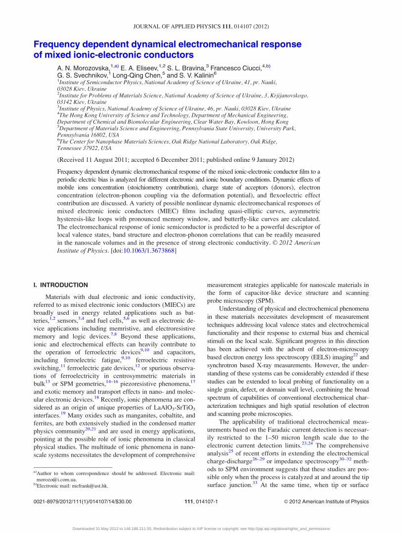
Here we consider planar configuration, corresponding to
the top electrode on the MIEC film. These structures are now
actively fabricated for impedance based studies,82,83 and can
also be used for focused X-ray (e.g. Ref. 84 for ferroelectric
materials and Ref. 85 for semiconductor nanostructures)
interferrometric and vibrometric detection. We further note
that the fully 1 D case implies no lateral current and ionic
transport from the edges (or completely blocking lateral
walls), whereas the deposited electrode can allow for lateral
transport at the edges. This affects conservation laws for
electrons and ionic species. The SPM experiment with local-
ized tip corresponds to the limiting case of a very small
electrode.
Geometry of the considered asymmetric heterostructure
electrode/possible gap/ionic semiconductor film/substrate elec-
trode is shown in Fig. 1(a). Electric potential V is applied to
the top planar microelectrode. The substrate electrode
located at z¼ h is grounded, V¼ 0. The semiconductor film
of thickness h is regarded thick enough to have a continuous
band structure [Fig. 1(b)]. The existence of vacuum or air
dielectric gap of thickness H between the charged top micro-
electrode and the MIEC film is also possible, mirroring
FIG. 1. (Color online) (a) Geometry of
the considered asymmetric heterostruc-
ture “tip electrode/gap/ionic semicon-
ductor film/substrate electrode.” (b)
Schematic bend structure at z¼ 0:
U ¼ Am=eþ V, where Am is the work
function difference, VðtÞ ¼ V0 sin xtð Þisthe voltage difference applied to the tip
electrode at z¼ -H, u is the electric
potential, v is the electron affinity in the
semiconductor.
014107-3 Morozovska et al. J. Appl. Phys. 111, 014107 (2012)
Downloaded 31 May 2012 to 146.186.211.55. Redistribution subject to AIP license or copyright; see http://jap.aip.org/about/rights_and_permissions
models for imperfect contact or dead layer in ferroelectric
materials.86,87
Here, free electrons in the conductive band (n) and holes
(p) in the valence band consider which quasi-levels can be
different and coordinate dependent in the dynamic case. The
acceptors (donors) are neutral or singly ionized. The neutral
acceptors (donors) are immobile, and the charged ones could
be mobile or almost immobile.8
A. Dynamic electromechanical responsein decoupling approximation: Flexoelectric, Vegard,and electron-phonon contributions
Decoupling approximation has been recently used for
MIECs (Refs. 56 and 67) and much earlier for the local elec-
tromechanical response calculations of ferroelectrics.88–94
As the sort of perturbation approach, it consists of two suc-
cessive stages. On the first stage one neglects the elastic
stresses originated from electrostriction, piezoelectric effect
(for ferroelectrics) and flexoelectric effects and Vegard
expansion, in order to calculate the electric potential and mo-
bile charges distribution. On the second stage all these
effects are taken into account when the system strain is cal-
culated using the electric potential and mobile charges distri-
bution calculated on the first stage. The accuracy of the
decoupling approximation is surprisingly high even for ferro-
electrics (error is proportional to the squire of the electrome-
chanical coupling coefficient) and approved by other
numerical methods like phase-field and FEM.95 Earlier we
studied the accuracy of the decoupling approximation for
paraelectric SrTiO3 and proved that it is valid with several %
accuracy at film thicknesses more than several screening
radius and moderate applied voltages. Moreover, the decou-
pling approximation is valid with very high accuracy at arbi-
trary thicknesses and voltages after the substitution of the
LGD-expansion coefficient a(T) with aP ¼ a Tð Þ þ3~a11 Ph i2in the electrostriction contribution term (see designations
and Fig. 2 in Ref. 67).
We suppose that the total stress tensor rijðrÞ is linearly
proportional to the Vegard contribution, electron-phonon
contribution, flexoelectric and electrostriction contributions,
rijðrÞ¼cijkluklðrÞþ
NCij ðnðrÞ�n0ÞþNV
ij ðpðrÞ�p0Þþ
�baijðN�a ðrÞ�N�a0Þ�bd
ijðNþd ðrÞ�Nþd0Þ
!
�cijkl
@2u@xk@xl
þ ~qijkl@u@xk
@u@xl
: (1)
Here cijkl is the tensor of elastic stiffness, uklðrÞ is the strain
tensor, NC;Vij is a tensor deformation potential of electrons in
the conduction (C) and valence bands (V), ba;dij are the
Vegard expansion tensors for acceptors (donors). Nþd rð Þ is
the instant concentration of mobile ionized donors, N�a rð Þ is
the instant concentration of mobile ionized acceptors, Nþd0
and N�a0 are their stoichiometric equilibrium concentrations;
n rð Þ is the concentration of electrons in the conduction band,
p rð Þ is the concentration of holes in the valence band, n0 and
p0 are their equilibrium concentrations, u rð Þ is the electric
potential. Flexoelectric strain tensor cijkl has been measured
experimentally for several substances and it was found to
vary by several orders of magnitude from 10�11 C/m to
10�6 C/m.96–98
~qijkl is the electrostriction tensor that couples stress and
electric field. It is related to the electrostriction tensor qijkl,
that couples strain and polarization, via the dielectric sus-
ceptibility vij ¼ e0 eij � dij
� �as ~qijkl ¼ vipvjqqpqkl (eij is the
dielectric permittivity). In fact the electrostriction coeffi-
cients for typical semiconductors with low dielectric permit-
tivity (smaller than several tens) are such that the
electrostriction contribution becomes essential only at high
electric fields (see, e.g., Refs. 99 and 100). However for
paraelectrics with high dielectric permittivity eij, e.g., for
SrTiO3, electrostriction contribution can be dominant even at
moderate electric fields.67
Note, that Eq. (1) requires the reference crystallographic
lattice to be defined, as analyzed for pure diffusion-stress
coupling by Larche and Cahn.101 The reference lattice is
regarded strain-free for the case of zero electric potential:
u ¼ 0 and therefore n rð Þ ¼ n0; p rð Þ ¼ p0; N�a rð Þ ¼ N�a0;Nþd rð Þ ¼ Nþd0.
Lame-type equation for the electromechanical displace-
ment ui can be obtained from the equation of mechanical
equilibrium @rijðrÞ=@xi ¼ 0, where the stress tensor rijðrÞ is
given by Eq. (1). Mechanical boundary conditions102 corre-
sponding to the ESM experiments23 are defined on the
mechanically free interface, z¼ 0, where the normal stress
r3i is absent, and on clamped interface z¼ h, where the dis-
placement ui is fixed,
r3i x1; x2; z ¼ 0ð Þ ¼ 0; ui x1; x2; z ¼ hð Þ ¼ 0: (2)
Using the decoupling approximation in the 1D-Poisson equa-
tion for the electric potential, mechanical displacement of
the MIEC surface caused by the flexoelectric, electronic, and
ionic contributions was calculated as56
u3ðz ¼ 0Þ �ðh
0
dz0
c33
nC n z0ð Þ � n0ð Þ þ nV p z0ð Þ � p0ð Þ�la N�a z0ð Þ � N�a0
� �þld Nþd z0ð Þ � Nþd0
� �þ ~q33
@u z0ð Þ@z0
� �2
0BB@
1CCA:(3)
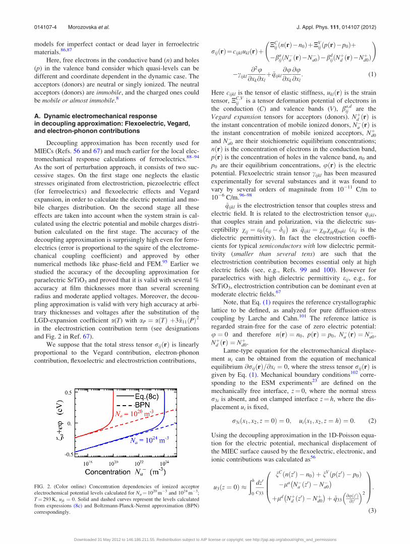
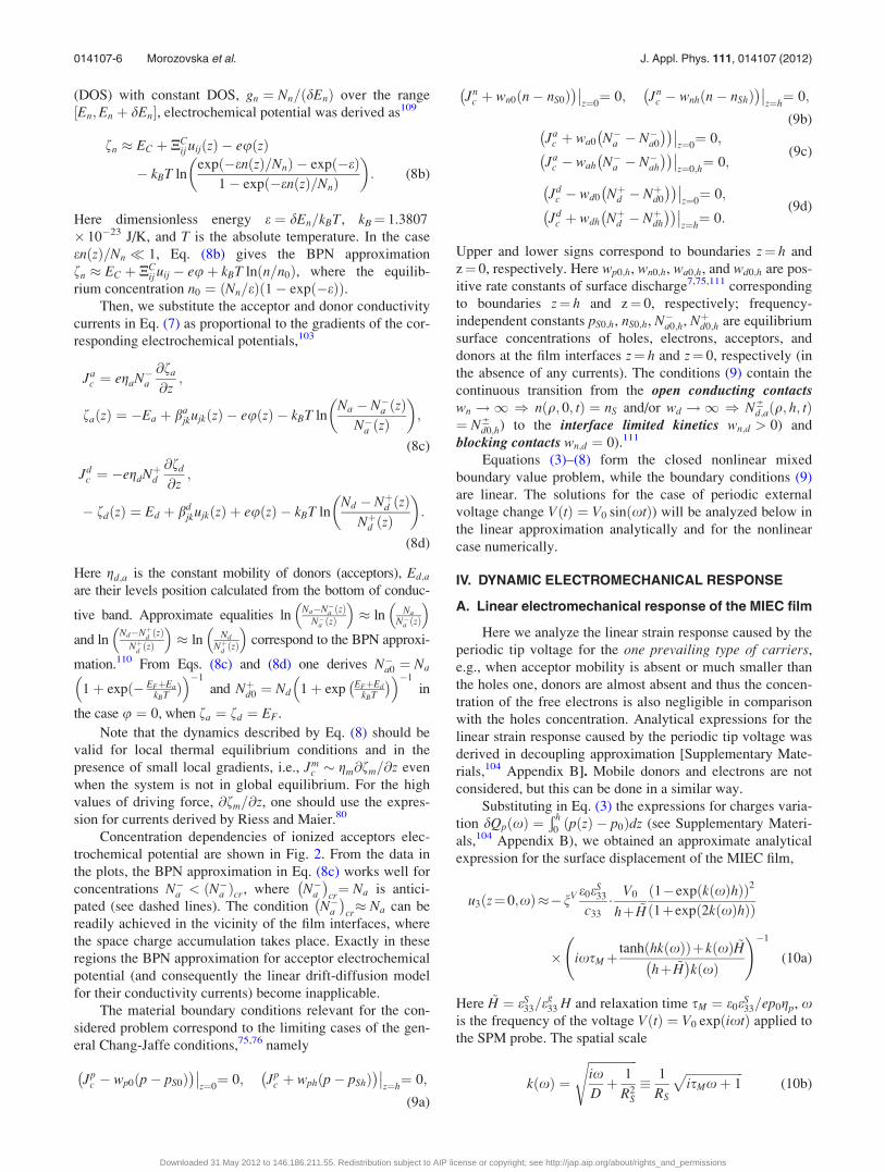
FIG. 2. (Color online) Concentration dependencies of ionized acceptor
electrochemical potential levels calculated for Na¼ 1020 m�3 and 1024 m�3;
T¼ 293 K, ujk ¼ 0. Solid and dashed curves represent the levels calculated
from expressions (8c) and Boltzmann-Planck-Nernst approximation (BPN)
correspondingly.
014107-4 Morozovska et al. J. Appl. Phys. 111, 014107 (2012)
Downloaded 31 May 2012 to 146.186.211.55. Redistribution subject to AIP license or copyright; see http://jap.aip.org/about/rights_and_permissions

Here e is the electron charge absolute value, constants
nC ��NC
33 �c3333eeS
33e0
�, nV �
�NV
33 þc3333eeS
33e0
�, la �
�ba
33 þc3333eeS
33e0
�,
and ld ���bd
33 þc3333eeS
33e0
�, eS
33 is the universal dielectric
constant.
From Eq. (3) the MIEC surface displacement is propor-
tional to the total charge of each species. Note, that the rela-
tion between the total charge and electrostatic potential on
the semiconductor surface is well established.103 Note, that
the first terms in material constants nC;V originated from the
deformation potential or Vegard tensors, while the last ones
originated from the flexoelectric coupling. Remarkably, that
the strength of tensorial deformation potential NC;V33 appeared
comparable to the Vegard tensor ba;d33 or even higher.
Note, that for ion-blocking electrodes the total number
of ions remains the same, i.e.,Ð h
0N�a zð Þ�N�a0
� �dz¼ 0 andÐ h
0Nþd zð Þ�Nþd0
� �dz¼ 0 when neglecting generation recombi-
nation effects. No such constrains exist for the case when
one or two electrodes are ion conducting.
Note, that in principle, the impedance spectroscopy
formalism78,105,106 can be used to derive the linear electro-
mechanical response. However, for MIECs this approach
requires the distributed models (e.g., see Ref. 107 for a
detailed review), since lumped element models generally fail
to reproduce the coupled electronic-ionic transport. This
approach is then mathematically equivalent to the direct so-
lution of coupled transport equations. Typically distributed
circuit models also impose the electroneutrality condition,
which is not the case at least near interfaces of MIEC thin
films. However, in order to calculate the nonlinear electro-
mechanical response in MIECs the impedance spectroscopy
formalism should be modified to account for nonlinearity,108
since the impedance relations V tð Þ � I tð Þ � R tð Þ for I-V
curves and mechanical displacement, as proportional to the
total charge Q tð Þ of each species, u3 tð Þ � Q tð Þ �Ð t
I yð Þdy�Ð t
V yð Þ � R�1 yð Þdy, are valid in the time domain only. The
convolution theorem for u3 xð Þ should be applied in the spec-
tral frequency domain, which breaks the proportionality
u3 xð Þ � 1=ixR allowing for the complex nonlinear temporal
dependence of the impedance R tð Þ.
B. Poisson equations and electrodynamics boundaryconditions
For frequencies less than 1 MHz, which is a typical
operating limit for these experiments, the quasi-static
approximation for the electric field Ez ¼ �@/ rð Þ=@z works
with high accuracy. Neglecting the flexoelectric term (decou-
pling approximation), the 1 D-Laplace equation in the
dielectric gap (if any) and the 1 D-Poisson equation in MIEC
film have the form,
d2udz2¼ 0; �H < z < 0 ðgapÞ (4a)
d2udz2¼ � qðuÞ
eS33e0
; 0 < z < h ðMIEC filmÞ: (4b)
Here u zð Þ is the electric potential and eS33 is MIEC dielectric
permittivity. The charge density in the MIEC film has the form,
q zð Þ ¼ e p zð Þ � n zð Þ � N�a zð Þ þ Nþd zð Þ� �
: (5)
The boundary conditions for the electrostatic potential uðzÞare u z ¼ hð Þ ¼ 0 on the grounded substrate electrode,
u z ¼ �Hð Þ ¼ Am=eþ V on the tip electrode-dielectric gap-
film, u z ¼ þ0ð Þ � u z ¼ �0ð Þ � Vb on the tip electrode-
dielectric gap-film, and
D2n � D1n ¼ �e0 eS33
@uðz ¼ þ0Þ@z
� eg33
@uðz ¼ �0Þ@z
� �¼ 0
(6)
on the film-dielectric gap boundary. Here, Am is the work
function from the conducting tip electrode that typically
determines the contact built-in potential Vb, VðtÞ¼ V0 sin xtð Þis the periodic voltage difference applied to the
tip electrode at z¼�H, eg33is the dielectric constant of the
dielectric layer. The normal vector n is pointed from media 1
to media 2. The free surface charge is regarded absent at
z¼ 0 in the dynamic case. Note, that the potential can be
always set zero at the contact z¼ h, while the contact itself
may either have contact barrier or barrierless (ohmic).
C. Kinetic equations and boundary conditions
The total electric current of the MIEC film is Jf ¼JDs
þJc, where JDs z; tð Þ¼e0eS;g33 @Ez=@tð Þ is the displacement cur-
rent (existing both in the dielectric and in the MIEC), and
Jc z; tð Þ is the conductivity current that exists in the MIEC
only. The continuity equation @q=@tð Þ þ @Jc=@zð Þ¼0 should
be solved along with all electrodynamics equations.
The conductivity current Jc z; tð Þ ¼P
m¼a;p;d;n Jmc con-
sists of the acceptor (Jac ), hole (Jp
c ), donor (Jdc ), and electron
(Jnc ) currents. Under negligibly small impact of the electron-
hole recombination-generation process charges conservation
equations are
� @N�a@tþ 1
e
@Jac
@z¼ 0; (7a)
@p
@tþ 1
e
@Jpc
@z¼ 0; (7b)
@Nþd@tþ 1
e
@Jdc
@z¼ 0; (7c)
� @n
@tþ 1
e
@Jnc
@z¼ 0: (7d)
The electron and hole conductivity currents are proportional
to the gradients of the carrier electrochemical potentials lev-
els as Jpc ¼ �egpp @fp=@z
� �; and Jn
c ¼ egnn @fn=@zð Þ;where gn;p is the constant mobility of electrons (holes) and
� fp zð Þ � NVij uij zð Þ þ eu zð Þ þ kBT ln
p zð Þp0
� �: (8a)
Note that holes in the quasi-Fermi levels Eq. (8a) are typi-
cally defined in the BPN approximation, since they are
mostly not degenerated in the MIECs.
At the same time, the electrons in the correlated oxides
are well-localized. Using the rectangular density of states
014107-5 Morozovska et al. J. Appl. Phys. 111, 014107 (2012)
Downloaded 31 May 2012 to 146.186.211.55. Redistribution subject to AIP license or copyright; see http://jap.aip.org/about/rights_and_permissions
(DOS) with constant DOS, gn ¼ Nn= dEnð Þ over the range
En;En þ dEn½ �, electrochemical potential was derived as109
fn � EC þ NCij uij zð Þ � eu zð Þ
� kBT lnexp �en zð Þ=Nnð Þ � exp �eð Þ
1� exp �en zð Þ=Nnð Þ
� �: (8b)
Here dimensionless energy e ¼ dEn=kBT, kB¼ 1.3807
� 10�23 J/K, and T is the absolute temperature. In the case
en zð Þ=Nn 1, Eq. (8b) gives the BPN approximation
fn � EC þ NCij uij � euþ kBT ln n=n0ð Þ, where the equilib-
rium concentration n0 ¼ Nn=eð Þ 1� exp �eð Þð Þ.Then, we substitute the acceptor and donor conductivity
currents in Eq. (7) as proportional to the gradients of the cor-
responding electrochemical potentials,103
Jac ¼ egaN�a
@fa
@z;
fa zð Þ ¼ �Ea þ bajkujk zð Þ � eu zð Þ � kBT ln
Na � N�a zð ÞN�a zð Þ
� �;
(8c)
Jdc ¼ �egdNþd
@fd
@z;
� fd zð Þ ¼ Ed þ bdjkujk zð Þ þ eu zð Þ � kBT ln
Nd � Nþd zð ÞNþd zð Þ
� �:
(8d)
Here gd;a is the constant mobility of donors (acceptors), Ed;a
are their levels position calculated from the bottom of conduc-
tive band. Approximate equalities ln�
Na�N�a ðzÞN�a ðzÞ
�� ln
�Na
N�a ðzÞ
�and ln
�Nd�Nþ
dðzÞ
NþdðzÞ
�� ln
�Nd
NþdðzÞ
�correspond to the BPN approxi-
mation.110 From Eqs. (8c) and (8d) one derives N�a0 ¼ Na�1þ expð� EFþEa
kBT ��1
and Nþd0 ¼ Nd
�1þ exp
�EFþEd
kBT
���1
in
the case u ¼ 0, when fa ¼ fd ¼ EF.
Note that the dynamics described by Eq. (8) should be
valid for local thermal equilibrium conditions and in the
presence of small local gradients, i.e., Jmc � gm@fm=@z even
when the system is not in global equilibrium. For the high
values of driving force, @fm=@z, one should use the expres-
sion for currents derived by Riess and Maier.80
Concentration dependencies of ionized acceptors elec-
trochemical potential are shown in Fig. 2. From the data in
the plots, the BPN approximation in Eq. (8c) works well for
concentrations N�a < ðN�a Þcr, where N�a� �
cr¼ Na is antici-
pated (see dashed lines). The condition N�a� �
cr� Na can be
readily achieved in the vicinity of the film interfaces, where
the space charge accumulation takes place. Exactly in these
regions the BPN approximation for acceptor electrochemical
potential (and consequently the linear drift-diffusion model
for their conductivity currents) become inapplicable.
The material boundary conditions relevant for the con-
sidered problem correspond to the limiting cases of the gen-
eral Chang-Jaffe conditions,75,76 namely
Jpc � wp0 p� pS0ð Þ
� ���z¼0¼ 0; Jp
c þ wph p� pShð Þ� ���
z¼h¼ 0;
(9a)
Jnc þ wn0 n� nS0ð Þ
� ���z¼0¼ 0; Jn
c � wnh n� nShð Þ� ���
z¼h¼ 0;
(9b)
Jac þ wa0 N�a � N�a0
� �� ���z¼0¼ 0;
Jac � wah N�a � N�ah
� �� ���z¼0;h¼ 0;
(9c)
Jdc � wd0 Nþd � Nþd0
� �� ���z¼0¼ 0;
Jdc þ wdh Nþd � Nþdh
� �� ���z¼h¼ 0:
(9d)
Upper and lower signs correspond to boundaries z¼ h and
z¼ 0, respectively. Here wp0;h, wn0;h, wa0;h, and wd0;h are pos-
itive rate constants of surface discharge7,75,111 corresponding
to boundaries z¼ h and z¼ 0, respectively; frequency-
independent constants pS0;h, nS0;h, N�a0;h, Nþd0;h are equilibrium
surface concentrations of holes, electrons, acceptors, and
donors at the film interfaces z¼ h and z¼ 0, respectively (in
the absence of any currents). The conditions (9) contain the
continuous transition from the open conducting contactswn !1 ) n q; 0; tð Þ ¼ nS and/or wd !1 ) N6
d;aðq; h; tÞ¼ N6
d0;h) to the interface limited kinetics wn;d > 0) and
blocking contacts wn;d ¼ 0).111
Equations (3)–(8) form the closed nonlinear mixed
boundary value problem, while the boundary conditions (9)
are linear. The solutions for the case of periodic external
voltage change VðtÞ ¼ V0 sin xtð Þ) will be analyzed below in
the linear approximation analytically and for the nonlinear
case numerically.
IV. DYNAMIC ELECTROMECHANICAL RESPONSE
A. Linear electromechanical response of the MIEC film
Here we analyze the linear strain response caused by the
periodic tip voltage for the one prevailing type of carriers,
e.g., when acceptor mobility is absent or much smaller than
the holes one, donors are almost absent and thus the concen-
tration of the free electrons is also negligible in comparison
with the holes concentration. Analytical expressions for the
linear strain response caused by the periodic tip voltage was
derived in decoupling approximation [Supplementary Mate-
rials,104 Appendix B]. Mobile donors and electrons are not
considered, but this can be done in a similar way.
Substituting in Eq. (3) the expressions for charges varia-
tion dQp xð Þ ¼Ð h
0p zð Þ � p0ð Þdz (see Supplementary Materi-
als,104 Appendix B), we obtained an approximate analytical
expression for the surface displacement of the MIEC film,
u3ðz¼0;xÞ��nV e0eS33
c33
� V0
hþ ~H
1�exp k xð Þhð Þð Þ2
1þexp 2k xð Þhð Þð Þ
� ixsMþtanh hk xð Þð Þþk xð Þ ~H
hþ ~H� �
k xð Þ
!�1
(10a)
Here ~H ¼ eS33=e
g33 H and relaxation time sM ¼ e0eS
33=ep0gp, xis the frequency of the voltage VðtÞ ¼ V0 exp ixtð Þ applied to
the SPM probe. The spatial scale
k xð Þ ¼ffiffiffiffiffiffiffiffiffiffiffiffiffiffiffiffiixDþ 1
R2S
s� 1
RS
ffiffiffiffiffiffiffiffiffiffiffiffiffiffiffiffiffiffiffiisMxþ 1
p(10b)
014107-6 Morozovska et al. J. Appl. Phys. 111, 014107 (2012)
Downloaded 31 May 2012 to 146.186.211.55. Redistribution subject to AIP license or copyright; see http://jap.aip.org/about/rights_and_permissions
is defined by the diffusion coefficient D ¼ gp kBT=eð Þ and
Debye screening radius RS ¼ffiffiffiffiffiffiffiffiffiffiffiffiffiffiffiffiffiffiffiffiffiffiffiffiffiffiffiffieS
33e0kBT=e2p0
q.
In the approximate expression (10a) we should neglect
electrostriction, because in the linear approximation and
under the absence of built-in static electric field, the electro-
striction response will be manifested at frequencies doubled
in comparison with the frequency of the excitation electric
field. In the linear regime the double-frequency signal can be
excluded experimentally. Analytical results obtained from
Eqs. (10) are justified, if the hole conductivity is constant
proportional to the mobility and average concentration of
holes, while the acceptor conductivity is negligibly small in
comparison with the hole one. Otherwise numerical model-
ing of the nonlinear problem should be performed.
Note, that Eqs. (10) are derived for the case
Jcx 0ð Þ ¼ 0; qS hð Þ ¼ 0, where the space charge density
qS hð Þ ¼ e �N�a hð Þ þ p hð Þ� �
. Other types of the boundary
conditions, e.g., qS 0ð Þ ¼ qS hð Þ ¼ 0 and Jcx 0ð Þ ¼ Jc
x hð Þ ¼ 0,
lead to the total charge absence and consequently to zero sur-
face displacement u3ðxÞ ¼ 0 in the linear decoupling approx-
imation (see Table C1 in Supplementary Materials104).
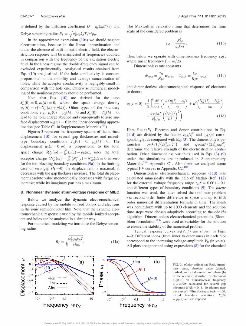
Figures 3 represent the frequency spectra of the surface
displacement (10) for several gap thicknesses and mixed-
type boundary conditions Jcx 0ð Þ ¼ 0, qS hð Þ ¼ 0. The
displacement u3ðz ¼ 0;xÞ is proportional to the total
space charge dQp xð Þ ¼Ð h
0p zð Þ � p0ð Þdz, since the total
acceptor charge dN�a xð Þ ¼Ð h
0N�a zð Þ � N�a0
� �dz � 0 is zero
for the ion-blocking boundary conditions (9a). In the limiting
case of zero gap (H!0) the displacement is maximal; it
decreases with the gap thickness increase. The total displace-
ment absolute value monotonically decreases with frequency
increase; while its imaginary part has a maximum.
B. Nonlinear dynamic strain-voltage response of MIEC
Below we analyze the dynamic electromechanical
response caused by the mobile ionized donors and electrons
in the ionic semiconductor film. Note, that the dynamic elec-
tromechanical response caused by the mobile ionized accept-
ors and holes can be analyzed in a similar way.
For numerical modeling we introduce the Debye screen-
ing radius
RS ¼
ffiffiffiffiffiffiffiffiffiffiffiffiffiffiffiffiffieS
33e0kBT
e2n0
s: (11a)
The Maxwellian relaxation time that determines the time
scale of the considered problem is
sM ¼R2
Se
gnkBT: (11b)
Thus below we operate with dimensionless frequency sMf ,
where linear frequency f ¼ x=2p.
Dimensionless rate constants
~wn0;h ¼sM
RSewn0;h; ~wd0;h ¼
sM
RSewd0;h; (11c)
and dimensionless electromechanical response of electrons
or donors
u3ðz ¼ 0Þ � 1
2
ðh
0
d~z
c33
nC n ~zð Þ � n0
n0
� �þ ld Nþd ~zð Þ � Nþd0
n0
� ��
þ ~q33kBT
eS33e0
@ ~u ~zð Þ@~z
� �2!: (11d)
Here ~z ¼ z=RS. Electron and donor contributions in Eq.
(11d) are divided by the factors c33=nC and c33=ld corre-
spondingly, as compared with Eq. (3). The dimensionless pa-
rameters ~q33kBT= 2eS33e0n
C� �
and ~q33kBT= 2eS33e0ld
� �determine the relative strength of the electrostriction contri-
bution. Other dimensionless variables used in Eqs. (3)–(9)
under the simulations are introduced in Supplementary
Materials,104 Appendix C1. Also there we analyzed some
typical I-V curves in Appendix C2.104
Dimensionless electromechanical response (11d) was
calculated numerically with the help of Matlab (Ref. 112)
for the external voltage frequency range sMf ¼ 0.001� 0.1
and different types of boundary conditions (9). The pdepefunction was used, the latter solved the nonlinear problem
via second order finite difference in space and up to fifth
order numerical differentiation formula in time. The mesh
was nonuniform with up to 1000 elements and the solution
time steps were chosen adaptively according to the ode15s
algorithm. Dimensionless electrochemical potentials (Sloot-
blom formulation113) were used as variables for the solution
to ensure the stability of the numerical problem.
Typical response curves ~u3 V; fð Þ are shown in Figs.
4–9. Different loops (from inner to outer ones) in each plot
correspond to the increasing voltage amplitude V0 (in volts).
All plots are generated using expressions (8) for the chemical
FIG. 3. (Color online) (a) Real, imagi-
nary parts, absolute value (dotted,
dashed, and solid curves) and phase (b)
of the normalized surface displacement
u3ð0;xÞ vs dimensionless frequency
w ¼ x=2p calculated for several gap
thickness ~H=RS ¼ 0, 1, 10 (figures near
the curves). Film thickness h=RS¼ 100,
mixed boundary conditions Jcx 0ð Þ
¼ qS hð Þ ¼ 0 are imposed.
014107-7 Morozovska et al. J. Appl. Phys. 111, 014107 (2012)
Downloaded 31 May 2012 to 146.186.211.55. Redistribution subject to AIP license or copyright; see http://jap.aip.org/about/rights_and_permissions

potential of carriers. The differences in loop shape mainly
originate from the type of boundary conditions, external volt-
age frequency, and film thickness as discussed in Secs. IV B
1–IV B 3.
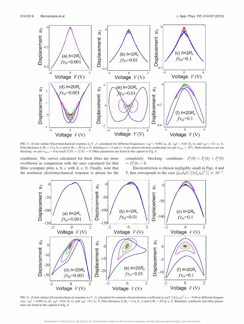
In Figs. 4, 5, 7, and 8 we neglect the electrostriction
impact into the electromechanical response (possible case of
dielectrically linear materials, like yttria-stabilized zirconia,
LiCoO2, LiMn2O4, LiC6). Electrostriction contribution is
included in Figs. 6, 9 and 10 for material parameters
nC¼ 10 eV, ld ¼ 10 eV (recalculated from known flexoelec-
tric coefficients and the data of Ref. 114), q33¼�13.7 109 m
J/C2 and e33 ¼ 300 corresponding to SrTiO3 with oxygen
vacancies. Since the oxygen vacancy concentration (and cor-
responding conductivity) can be tuned in the wide range for
SrTiO3,115,116 we cannot define sM for all cases, but rather
consider the range sMf ¼ 0.001� 0.1.
1. Ion-blocking and electron-conducting interfaces
The hysteresis-like loops, shown in Figs. 4, are calcu-
lated for the case of asymmetric mixed-type electronic
boundary conditions (9): interface z¼ 0 is almost electron
blocking (“almost” means that results remained the same
when we put ~wn0 10�2 in Eq. (9b)), interface z¼ h is
almost electron conducting (we put ~wnh � 102); both interfa-
ces are ion blocking: we put wd0;h ¼ 0 to reach
Jdc 0ð Þ ¼ Jd
c hð Þ ¼ 0. Different loops (from inner to outer
ones) correspond to the different values of maximal voltage
V0. Plots (a, b, c) are generated for thin film (h¼ 2RS) and
plots (d, e, f) for thicker ones (h¼ 20RS). The loop shape is
quasi-ellipsoidal only at small voltage amplitudes
V0 < kBT=e and becomes asymmetric hysteresis-like with V0
increase for f sM 0.01. The loops become noticeably open
(or even circle-like) with the frequency increase f sM � 0.01.
The loop opening becomes much stronger with the thick-
nesses increase. Note, that the response curves are strongly
asymmetric with respect to the voltage sign V ! �V, as can
be expected from the asymmetry of the interface electronic
conductivity. We further emphasize that the donor blocking
boundary conditions (Jdc 0ð Þ ¼ Jd
c hð Þ ¼ 0) and negligible
generation-recombination effects, the continuity equation
rules that d=dtð ÞÐ h
0Nþd ðzÞdz ¼ 0 and ionized donors contrib-
ute nothing to the response u3ðV; f Þ. Thus, only the total
changes of the electron amount contribute into the MIEC
film surface displacement.
The response curves u3ðV; f Þ, shown in Fig. 5, are sym-
metric with respect to the voltage sign V ! �V, since the
curves are calculated for the case of symmetric electron con-
ducting and ion-blocking interfaces at z¼ 0 and z¼ h. Note,
that for this case the gaps should be absent. Different loops
(black, red, green, and blue ones) correspond to the different
values of maximal voltage V0. Plots (a, b, c) are generated
for thin film (h¼ 2RS) and plots (d, e, f) for thicker ones
(h¼ 20RS). The curves calculated for low frequencies sMf¼ 0.001–0.01 are symmetric with respect to the voltage sign
even after the first cycling. The curves generated at higher
frequencies sMf ¼ 0.1 become symmetric with respect to the
voltage sign only after relatively long relaxation of the initial
FIG. 4. (Color online) Electromechanical response ~u3 V; fð Þ calculated for different frequencies: sMf ¼ 0.001 (a, d), sMf ¼ 0.01 (b, e), and sMf ¼ 0.1 (c, f).
Film thickness h=RS¼ 2 (a, b, c) and h=RS¼ 20 (d, e, f). Interface z¼ 0 is almost electron blocking, Jnc 0ð Þ ¼ 0 (we put ~wn0 10�2), interface z¼ h is almost
electron conducting (we put ~wnh � 102). Both interfaces are ion blocking: we put wd0;h ¼ 0 to reachJdc 0ð Þ ¼ Jd
c hð Þ ¼ 0. Band structure parameters: En ¼ 0 eV,
dEn ¼ 0.5 eV for electrons and Ed ¼ 0.1 eV for donors. Equilibrium surface concentrations are assumed to be equal to the bulk ones, full amounts ratio
Nd=Nn ¼ 0:1, mobilities ratio gd=gn ¼ 0:1. Also we neglected electrostriction contribution, ~q33¼ 0.
014107-8 Morozovska et al. J. Appl. Phys. 111, 014107 (2012)
Downloaded 31 May 2012 to 146.186.211.55. Redistribution subject to AIP license or copyright; see http://jap.aip.org/about/rights_and_permissions
conditions. The curves calculated for thick films are more
overblown in comparison with the ones calculated for thin
films (compare plots a, b, c with d, e, f). Finally, note that
the nonlinear electromechanical response is absent for the
completely blocking conditions Jnc 0ð Þ ¼ Jn
c hð Þ ¼ Jdc 0ð Þ
¼ Jdc hð Þ ¼ 0.
Electrostriction is chosen negligibly small in Figs. 4 and
5, that corresponds to the case ~q33kBT= 2eS33e0n
C� ��� �� 10�3.
FIG. 5. (Color online) Electromechanical response ~u3 V; fð Þ calculated for different frequencies: sMf ¼ 0.001 (a, d), sMf ¼ 0.01 (b, e), and sMf ¼ 0.1 (c, f).
Film thickness h=RS¼ 2 (a, b, c) and h=RS ¼ 20 (d, e, f). Interfaces z¼ 0 and z¼ h are almost electron conducting (we put ~wn0;h � 102). Both interfaces are ion
blocking: we put wd0;h ¼ 0 to reach Jdc 0ð Þ ¼ Jd
c hð Þ ¼ 0. Other parameters are listed in the caption to Fig. 4.
FIG. 6. (Color online) Electromechanical response ~u3 V; fð Þ calculated for nonzero electrostriction coefficient ~q33kBT= 2eS33e0n
C� �
¼�0.04 at different frequen-
cies: sMf ¼ 0.001 (a, d), sMf ¼0.01 (b, e), and sMf ¼0.1 (c, f). Film thickness h=RS ¼ 2 (a, b, c) and h=RS¼ 20 (d, e, f). Boundary conditions and other param-
eters are listed in the caption to Fig. 4.
014107-9 Morozovska et al. J. Appl. Phys. 111, 014107 (2012)
Downloaded 31 May 2012 to 146.186.211.55. Redistribution subject to AIP license or copyright; see http://jap.aip.org/about/rights_and_permissions
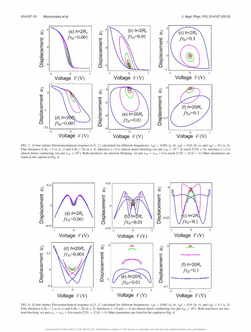
FIG. 8. (Color online) Electromechanical response ~u3 V; fð Þ calculated for different frequencies: sMf ¼ 0.001 (a, d), sMf ¼ 0.01 (b, e), and sMf ¼ 0.1 (c, f).
Film thickness h=RS ¼ 2 (a, b, c) and h=RS ¼ 20 (d, e, f). Interfaces z¼ 0 and z¼ h are almost donor conducting (we put ~wdh � 102). Both interfaces are elec-
tron blocking: we put wn0 ¼ wnh ¼ 0 to reach Jnc 0ð Þ ¼ Jn
c hð Þ ¼ 0. Other parameters are listed in the caption to Fig. 4.
FIG. 7. (Color online) Electromechanical response ~u3 V; fð Þ calculated for different frequencies: sMf ¼ 0.001 (a, d), sMf ¼ 0.01 (b, e), and sMf ¼ 0.1 (c, f).
Film thickness h=RS¼ 2 (a, b, c) and h=RS ¼ 20 (d, e, f). Interface z¼ 0 is almost donor blocking (we put ~wd0 10�2 to reach Jdc 0ð Þ � 0), interface z¼ h is
almost donor conducting (we put ~wdh � 102). Both interfaces are electron blocking: we put wn0 ¼ wnh ¼ 0 to reach Jnc 0ð Þ ¼ Jn
c hð Þ ¼ 0. Other parameters are
listed in the caption to Fig. 4.
014107-10 Morozovska et al. J. Appl. Phys. 111, 014107 (2012)
Downloaded 31 May 2012 to 146.186.211.55. Redistribution subject to AIP license or copyright; see http://jap.aip.org/about/rights_and_permissions
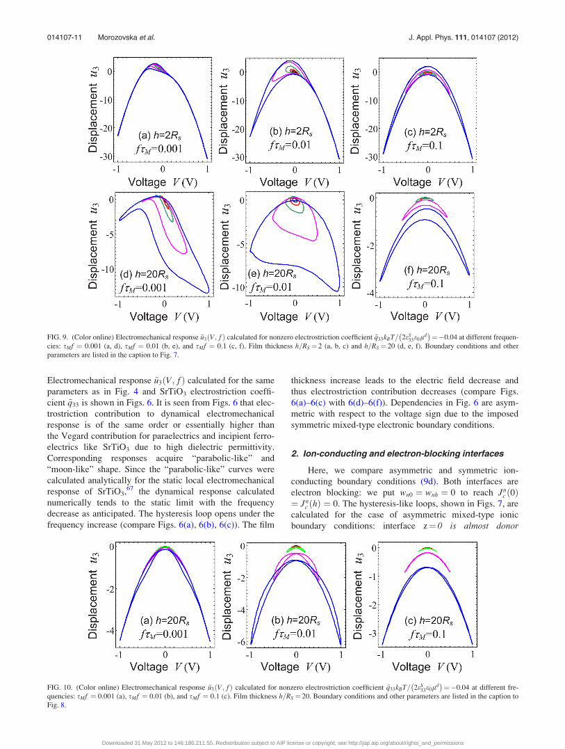
Electromechanical response ~u3 V; fð Þ calculated for the same
parameters as in Fig. 4 and SrTiO3 electrostriction coeffi-
cient ~q33 is shown in Figs. 6. It is seen from Figs. 6 that elec-
trostriction contribution to dynamical electromechanical
response is of the same order or essentially higher than
the Vegard contribution for paraelectrics and incipient ferro-
electrics like SrTiO3 due to high dielectric permittivity.
Corresponding responses acquire “parabolic-like” and
“moon-like” shape. Since the “parabolic-like” curves were
calculated analytically for the static local electromechanical
response of SrTiO3,67 the dynamical response calculated
numerically tends to the static limit with the frequency
decrease as anticipated. The hysteresis loop opens under the
frequency increase (compare Figs. 6(a), 6(b), 6(c)). The film
thickness increase leads to the electric field decrease and
thus electrostriction contribution decreases (compare Figs.
6(a)–6(c) with 6(d)–6(f)). Dependencies in Fig. 6 are asym-
metric with respect to the voltage sign due to the imposed
symmetric mixed-type electronic boundary conditions.
2. Ion-conducting and electron-blocking interfaces
Here, we compare asymmetric and symmetric ion-
conducting boundary conditions (9d). Both interfaces are
electron blocking: we put wn0 ¼ wnh ¼ 0 to reach Jnc 0ð Þ
¼ Jnc hð Þ ¼ 0. The hysteresis-like loops, shown in Figs. 7, are
calculated for the case of asymmetric mixed-type ionic
boundary conditions: interface z¼ 0 is almost donor
FIG. 9. (Color online) Electromechanical response ~u3 V; fð Þ calculated for nonzero electrostriction coefficient ~q33kBT= 2eS33e0ld
� �¼�0.04 at different frequen-
cies: sMf ¼ 0.001 (a, d), sMf ¼ 0.01 (b, e), and sMf ¼ 0.1 (c, f). Film thickness h=RS ¼ 2 (a, b, c) and h=RS ¼ 20 (d, e, f). Boundary conditions and other
parameters are listed in the caption to Fig. 7.
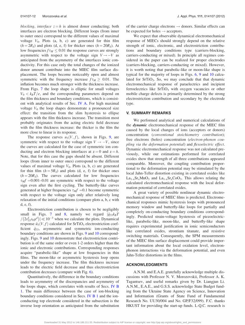
FIG. 10. (Color online) Electromechanical response ~u3 V; fð Þ calculated for nonzero electrostriction coefficient ~q33kBT= 2eS33e0ld
� �¼�0.04 at different fre-
quencies: sMf ¼ 0.001 (a), sMf ¼ 0.01 (b), and sMf ¼ 0.1 (c). Film thickness h=RS ¼ 20. Boundary conditions and other parameters are listed in the caption to
Fig. 8.
014107-11 Morozovska et al. J. Appl. Phys. 111, 014107 (2012)
Downloaded 31 May 2012 to 146.186.211.55. Redistribution subject to AIP license or copyright; see http://jap.aip.org/about/rights_and_permissions
blocking, interface z¼ h is almost donor conducting; both
interfaces are electron blocking. Different loops (from inner
to outer ones) correspond to the different values of maximal
voltage V0. Plots (a, b, c) are generated for thin film
(h¼ 2RS) and plots (d, e, f) for thicker ones (h¼ 20RS). At
low frequencies f sM 0.01 the response curves are strongly
asymmetric with respect to the voltage sign V!�V as
anticipated from the asymmetry of the interfaces ionic con-
ductivity. For this case only the total changes of the ionized
donor amount contribute into the MIEC film surface dis-
placement. The loops become noticeably open and almost
symmetric with the frequency increase f sM � 0.01. The
inflation becomes much stronger with the thickness increase.
From Figs. 7 the loop shape is elliptic for small voltages
V0 < kBT=e, and the corresponding parameters depend on
the film thickness and boundary conditions, which is consist-
ent with analytical results of Sec. IV A. For high maximal
voltage V0 the loop shapes demonstrate a pronounced size
effect: the transition from the slim hysteresis to ellipse
appears with the film thickness increase. The transition most
probably originates from the acting electric field decrease
with the film thickness increase: the thicker is the film the
more close to linear is its response.
The response curves u3ðV; f Þ, shown in Figs. 9, are
symmetric with respect to the voltage sign V ! �V, since
the curves are calculated for the case of symmetric ion con-
ducting and electron blocking interfaces at z¼ 0 and z¼ h.
Note, that for this case the gaps should be absent. Different
loops (from inner to outer ones) correspond to the different
values of maximal voltage V0. Plots (a, b, c) are generated
for thin film (h¼ 5RS) and plots (d, e, f) for thicker ones
(h¼ 20RS). The curves calculated for low frequencies
sMf ¼0.001–0.01 are symmetric with respect to the voltage
sign even after the first cycling. The butterfly-like curves
generated at higher frequencies sMf ¼0.1 become symmetric
with respect to the voltage sign only after relatively long
relaxation of the initial conditions (compare plots a, b, c with
d, e, f).
Electrostriction contribution is chosen to be negligibly
small in Figs. 7 and 8, namely we regard ~q33kBTj= 2eS
33e0ld� �
j10�3 when we calculate the plots. Dynamical
response ~u3 V; fð Þ calculated for SrTiO3 electrostriction coef-
ficient ~q33, asymmetric and symmetric ion-conducting
boundary conditions are shown in Figs. 9 and 10 correspond-
ingly. Figs. 9 and 10 demonstrate that electrostriction contri-
bution is of the same order or even 1-2 orders higher than the
ionic and electronic contributions. Corresponding responses
acquire “parabolic-like” shape at low frequencies in thin
films. The moon-like or asymmetric hysteresis loop opens
under the frequency increase. The film thickness increase
leads to the electric field decrease and thus electrostriction
contribution decreases (compare with Fig. 6).
Quantitatively, the difference in the boundary conditions
leads to asymmetry of the discrepancies and asymmetry of
the loops shape, which correlates with results of Secs. IV B
1. The main difference between the case of ion-blocking
boundary conditions considered in Secs. IV B 1 and the ion-
conducting top electrode considered in the subsection is the
inverse loop orientation as anticipated from the substitution
of the carrier charge electrons! donors. Similar effects can
be expected for holes! acceptors.
We expect that observable dynamical electromechanical
response of MIECs should strongly depend on the relative
strength of ionic, electronic, and electrostriction contribu-
tions and boundary conditions type (carriers-blocking,
carriers-conducting or mixed). In principle all regimes con-
sidered in the paper can be realized for proper electrodes
(carriers-blocking, carriers-conducting or mixed). However,
it is worth noting that parabolic-like or moon-like shape is
typical for the majority of loops in Figs. 6, 9 and 10 calcu-
lated for SrTiO3. So, we may conclude that that dynamic
electromechanical response of paraelectrics and incipient
ferroelectrics like SrTiO3 with oxygen vacancies or other
mobile charge defects is primarily determined by the strong
electrostriction contribution and secondary by the electrode
type.
V. SUMMARY REMARKS
We performed analytical and numerical calculations of
the dynamic electromechanical response of the MIEC film
caused by the local changes of ions (acceptors or donors)
concentration (conventional stoichiometry contribution);
free electrons (holes) concentration (electron-phonon cou-pling via the deformation potential) and flexoelectric effect.Dynamic electromechanical response was not calculated pre-
viously, while our estimations performed for correlated
oxides show that strength of all three contributions appeared
comparable. Moreover, the coupling contribution propor-
tional to the deformation potential may be stimulated by the
local Jahn-Teller distortion existing in correlated oxides like
La1-xSrxMnO3 and La1-xSrxCoO3. This allows relating the
calculated electromechanical response with the local defor-
mation potential of correlated oxides.
A great variety of possible nonlinear dynamic electro-
mechanical response of MIEC films is predicted. Electrome-
chanical responses mimic hysteresis loops with pronounced
memory window and butterfly-like loops for partially and
completely on-conducting boundary conditions correspond-
ingly. Predicted strain-voltage hysteresis of piezoelectric-
like, parabolic-like, moon-like, and butterfly-like shape
requires experimental justification in ionic semiconductors
like correlated oxides, strontium titanate, and resistive
switching materials. Consequently, the SPM measurements
of the MIEC film surface displacement could provide impor-
tant information about the local oxidation level, electron-
phonon interactions via the deformation potential, and even
Jahn-Teller distortions in the films.
ACKNOWLEDGMENTS
A.N.M. and E.A.E. gratefully acknowledge multiple dis-
cussions with Professor N. V. Morozovskii, Professor A. K.
Tagantsev, and useful remarks given by Dr. Liangjun Li.
A.N.M., E.A.E., and G.S.S. acknowledge State Budget fund-
ing from the Ukraine State Agency on Science, Innovation
and Information (Grants of State Fund of Fundamental
Research No. UU30/004 and No. GP/F32/099). F.C. thanks
HKUST for providing the start-up funds. L-Q.C. research is
014107-12 Morozovska et al. J. Appl. Phys. 111, 014107 (2012)
Downloaded 31 May 2012 to 146.186.211.55. Redistribution subject to AIP license or copyright; see http://jap.aip.org/about/rights_and_permissions
sponsored by the National Science Foundation (Materials
World Network, DMR-0908718). E.A.E. and A.N.M. further
acknowledge user agreement with CNMS No. UR-08-869.
Research supported (S.V.K.) by the U.S. Department of
Energy, Basic Energy Sciences, Materials Sciences and En-
gineering Division.
1G. A. Nazri and G. Pistoia, Lithium Batteries: Science and Technology(Springer-Verlag, New York, 2009).
2D. Y. Wang, J. Xiao, W. Xu, and J. G. Zhang, J. Electrochem. Soc. 157,
A760 (2010).3Solid State Electrochemistry I: Fundamentals, Materials and Their Appli-cations, edited by V. V. Kharton (Wiley-VCH, New York, 2009).
4A. Kolmakov, Y. X. Zhang, G. S. Cheng, and M. Moskovits, Adv. Mater.
15, 997 (2003).5V. S. Bagotsky, Fuel Cells: Problems and Solutions (Wiley, New York,
2009).6R. O’Hayre, S. W. Cha, W. Colella, and F. B. Prinz, Fuel Cell Fundamen-tals (Wiley, New York, 2009).
7Y. Gil, O. M. Umurhan, and I. Riess, Solid State Ionics 178, 1 (2007)8Y. Gil, O. M. Umurhan, and I. Riess, J. Appl. Phys. 104, 084504 (2008).9J. F. Scott, Ferroelectric Memories (Springer, Heidelberg, Germany,
2000).10A. K. Tagantsev, I. Stolichnov, E. L. Colla, and N. Setter, J. Appl. Phys.
90, 1387 (2001).11S. S. Nonnenmann, E. M. Gallo, and J. E. Spanier, Appl. Phys. Lett. 97,
102904 (2010).12X. Hong, J. Hoffman, A. Posadas, K. Zou, C. H. Ahn, and J. Zhu, Appl.
Phys. Lett. 97, 033114 (2010).13A. Soukiassian, A. K. Tagantsev, and N. Setter, Appl. Phys. Lett. 97,
192903 (2010).14R. F. Mamin, I. K. Bdikin, and A. L. Kholkin, Appl. Phys. Lett. 94,
222901 (2009).15A. L. Kholkin, I. K. Bdikin, T. Ostapchuk, and J. Petzelt, Appl. Phys.
Lett. 93, 222905 (2008).16R. Tararam, I. Bdikin, J. A. Varela, P. R. Bueno, J. Gracio, and A. Kholkin,
Mater. Res. Soc. Symp. Proc. 1255, 1255–M03-19 (2010).17J. S. Milne, A. C. H. Rowe, S. Arscott, and Ch. Renner, Phys. Rev. Lett.
105, 226802 (2010).18J. Yao, L. Zhong, D. Natelson, and J. M. Tour, J. Am. Chem. Soc. 133,
941 (2011).19F. Bi, D. F. Bogorin, C. Cen, C. W. Bark, J. W. Park, C. B. Eom, and
J. Levy, Appl. Phys. Lett. 97, 173110 (2010).20M. Imada, A. Fujimori, and Y. Tokura, Rev. Mod. Phys. 70, 1040 (1998).21J. B. Goodenough, Rep. Prog. Phys. 67, 1915 (2004).22Scanning Transmission Electron Microscopy: Imaging and Analysis,
edited by S. J. Pennycook and P. D. Nellist (Springer, New York, 2011).23A. N. Morozovska, E. A. Eliseev, and S. V. Kalinin, Appl. Phys. Lett. 96,
222906 (2010).24A. N. Morozovska, E. A. Eliseev, N. Balke, and S. V. Kalinin, J. Appl.
Phys. 108, 053712 (2010).25S. V. Kalinin and N. Balke, Adv. Mater. 22, E193 (2010).26K. Kuriyama, A. Onoue, Y. Yuasa, and K. Kushida, Surf. Sci. 601, 2256
(2007).27K. Kushida and K. Kuriyama, Appl. Phys. Lett. 84, 3456 (2004).28F. Vullum and D. Teeters, J. Power Sources 146, 804 (2005).29F. Vullum, D. Teeters, A. Nyten, and J. Thomas, Solid State Ionics 177,
2833 (2006).30R. Shao, S. V. Kalinin, and D. A. Bonnell, Appl. Phys. Lett. 82, 1869
(2003).31R. O’Hayre, M. Lee, and F. B. Prinz, J. Appl. Phys. 95, 8382 (2004).32K. Darowicki, M. Szocinski, and A. Zielinski, Electrochim. Acta 55,
3741 (2010).33M. W. Louie, A. Hightower, and S. M. Haile, ACS Nano 4, 2811 (2010).34R. V. Martinez and R. Garcia, Nano Letters 5, 1161 (2005).35R. V. Martinez, N. S. Losilla, J. Martinez, M. Tello, and R. Garcia, Nano-
technology 18, 084021 (2007).36R. Garcia, N. S. Losilla, J. Martinez, R. V. Martinez, F. J. Palomares, Y.
Huttel, M. Calvaresi, and F. Zerbetto, Appl. Phys. Lett. 96, 143110 (2010).37F. S. S. Chien, W. F. Hsieh, S. Gwo, A. E. Vladar, and J. A. Dagata,
J. Appl. Phys. 91, 10044 (2002).38M. Lee, R. O’Hayre, F. B. Prinz, and T. M. Gur, Appl. Phys. Lett. 85,
3552 (2004).
39R. Garcia, R. V. Martinez, and J. Martinez, Chem. Soc. Rev. 35, 29
(2006).40N. Balke, S. Jesse, Y. Kim, L. Adamczyk, A. Tselev, I. N. Ivanov,
N. Dudney, and S.V. Kalinin, Nano Letters 10, 3420 (2010).41N. Balke, S. Jesse, A. N. Morozovska, E. A. Eliseev, D. W. Chung,
Y. Kim, L. Adamczyk, R. E. Garcia, N. Dudney, and S.V. Kalinin, Nature
Nanotechnol. 5, 749 (2010).42A. Gruverman and A. Kholkin, Rep. Prog. Phys. 69, 2443 (2006).43A. Gruverman and S. V. Kalinin, J. Mater. Sci. 41, 107 (2006).44S. V. Kalinin, B. J. Rodriguez, S. Jesse, B. Mirman, E. Karapetian,
E. A. Eliseev, and A. N. Morozovska, Annu. Rev. Mater. Sci. 37, 189
(2007).45A. Gruverman, O. Auciello, and H. Tokumoto, J. Vac. Sci. Technol. B
14, 602 (1996).46S. V. Kalinin, A. N. Morozovska, L. Q. Chen, and B. J. Rodriguez, Rep.
Prog. Phys. 73, 056502 (2010).47S. Y. Hu and L. Q. Chen, Acta Mater. 52, 3069 (2004).48B. C. Han, A. Van der Ven, D. Morgan, and G. Ceder, Electrochim. Acta
49, 4691 (2004).49X. Zhang, W. Shyy, and A. M. Sastry, J. Electrochem. Soc. 154, A910
(2007).50G. K. Singh, G. Ceder, and M. Z. Bazant, Electrochim. Acta 53, 7599
(2008).51X. Zhang, A. M. Sastry, and W. Shyy, J. Electrochem. Soc. 155, A542
(2008).52Y. T. Cheng and M. W. Verbrugge, J. Appl. Phys. 104, 083521 (2008).53Amit Kumar, Francesco Ciucci, A. N. Morozovska, Sergei Kalinin, and
Stephen Jesse, Nat. Chem. 3, 707 (2011).54Stephen Jesse, Nina Balke, Eugene Eliseev, Alexander Tselev, Nancy
J. Dudney, Anna N. Morozovska, and Sergei V. Kalinin, ACS Nano 5,
9682 (2011).55Dmitri B. Strukov, Gregory S. Snider, Duncan R. Stewart, and R. Stanley
Williams, Nature 453, 80 (2008).56A. N. Morozovska, E. A. Eliseev, A. K. Tagantsev, S. L. Bravina, Long-
Qing Chen, and S. V. Kalinin, Phys. Rev. B 83, 195313 (2011).57S. B. Adler, J. Am. Ceram. Soc. 84, 2117 (2001).58S. B. Adler, X. Y. Chen, and J. R. Wilson, J. Catal. 245, 91 (2007).59X. Chen, J. Yu, and S.B. Adler, Chem. Mater. 17, 4537 (2005).60Y. Ohno, S. Nagata, and H. Sato, Solid State Ionics 9&10, 1001 (1983).61L. Tai, M. Nasrallah, H. Anderson, D. Sparlin, and S. Sehlin, Solid State
Ionics 76, 273 (1995).62H. Nagamoto, I. Mochida, K. Kagotani, and H. Inoue, Mater. Res. 8,
3158 (1993).63S. R. Bishop, K. L. Duncan, and E. D. Wachsman, Electrochim. Acta 54,
1436 (2009).64D. J. Kim, J. Am. Ceram. Soc. 72, 1415 (1989).65S. J. Hong and A. V. Virkar, J. Am. Ceram. Soc. 78, 433 (1995).66M. H. R. Lankhorst, H. J. M. Bouwmeester, and H. Verweij, Phys. Rev.
Lett. 77, 2989 (1996).67A. N. Morozovska, E. A. Eliseev, G. S. Svechnikov, and S. V. Kalinin.
Phys. Rev. B 84, 045402 (2011).68J. F. Mitchell, D. N. Argyriou, C. D. Potter, D. G. Hinks, J. D. Jorgensen,
and S. D. Bader, Phys. Rev. B 54, 6172 (1996).69M. Vraear, A. Kuzmin, R. Merkle, J. Purans, E. A. Kotomin, J. Maier,
and O. Mathon, Phys. Rev. B 76, 174107 (2007).70Y. Okimoto, T. Katsufuji, T. Ishikawa, T. Arima, and Y. Tokura, Phys.
Rev. B 55, 4206 (1997).71J. M. Ziman, Principles of the Theory of Solids (University Press,
Cambridge, 1972), Chap. 6, item 14.72Y. Sun, S. E. Thompson, and T. Nishida, J. Appl. Phys. 101, 104503 (2007).73J. Svoboda, and F. D. Fischer, Acta Mater. 57, 4649 (2009).74A. G. Tangera, J. Middelhoek, and N. F. de Rooij, J. Appl. Phys. 49, 2876
(1978).75H. Ch. Chang and G. Jaffe, J. Chem. Phys. 20, 1071 (1952).76J. R. Macdonald, J. Chem. Phys. 58, 4982 (1973).77Z. Chen, J. Electrochem. Soc. 151, A1576 (2004).78J. Jamnik and J. Maier, J. Electrochem. Soc. 146, 4183 (1999).79D. R. Franceschetti and J. R. Macdonald, J. Appl. Phys. 50, 291 (1979).80I. Riess and J. Maier, Phys. Rev. Let. 100, 205901 (2008).81F. Ciucci, Y. Hao, and D. G. Goodwin. Phys. Chem. Chem. Phys. 11,
11243 (2009).82A. K. Opitz and J. Fleig, Solid State Ionics 181, 684 (2010).83G. J. La O’, H. J. In, E. Crumlin, S. Barbastathis, and Y. Shao Horn, Inter-
national Journal of Energy Research 31, 548 (2007).
014107-13 Morozovska et al. J. Appl. Phys. 111, 014107 (2012)
Downloaded 31 May 2012 to 146.186.211.55. Redistribution subject to AIP license or copyright; see http://jap.aip.org/about/rights_and_permissions
84A. Grigoriev, D. H. Do, D. M. Kim, C. B. Eom, B. Adams, E. M.
Dufresne, and P. G. Evans, Phys. Rev. Lett. 96, 187601 (2006).85C. E. Murray, A. Ying, S. M. Polvino, I. C. Noyan, M. Holt, and J. Maser,
J. Appl. Phys. 109, 083543 (2011).86A. K. Tagantsev and G. Gerra, J. Appl. Phys. 100, 051607 (2006).87E. A. Eliseev, A. N. Morozovska, G. S. Svechnikov, E. L. Rumyantsev,
E. I. Shishkin, V. Y. Shur, and S. V. Kalinin, Phys. Rev. B 78, 245409
(2008).88F. Felten, G. A. Schneider, J. Munoz Saldana, and S. V. Kalinin, J. Appl.
Phys. 96, 563 (2004).89D. A. Scrymgeour and V. Gopalan, Phys. Rev. B 72, 024103 (2005).90E. Karapetian, M. Kachanov, and S. V. Kalinin, Philos. Mag. 85, 1017
(2005).91S. V. Kalinin, E. Karapetian, and M. Kachanov, Phys. Rev. B 70, 184101
(2004).92S. V. Kalinin, E. A. Eliseev, and A. N. Morozovska, Appl. Phys. Lett. 88,
232904 (2006).93E. A. Eliseev, S. V. Kalinin, S. Jesse, S. L. Bravina, and A. N. Morozovska,
J. Appl. Phys. 102, 014109 (2007).94A. N. Morozovska, E. A. Eliseev, S. L. Bravina, and S. V. Kalinin, Phys.
Rev. B 75, 174109 (2007).95Lili Tian, Aravind Vasudevarao, Anna N. Morozovska, Eugene A. Eli-
seev, Sergei V. Kalinin, and Venkatraman Gopalan, J. Appl. Phys. 104,
074110 (2008).96A. K. Tagantsev, V. Meunier, and P. Sharma, MRS Bull. 34, 643 (2009).97N. D. Sharma, C. M. Landis, and P. Sharma. J. Appl. Phys. 108, 024304
(2010).98M. Gharbi, Z. H. Sun, P. Sharma, K. White, and S. El-Borgi, Int. J. Solids
Struct. 48, 249 (2011).99G. Dennler, C. Lungenschmied, N. S. Sariciftci, R. Schwodiauer, S.
Bauer, and H. Reiss, Appl. Phys. Lett. 87, 163501 (2005).100K. Schwarz, U. Rabe, S. Hirsekorn, and W. Arnold, Appl. Phys. Lett. 92,
183105 (2008).101F. Larche and J. W. Cahn, Acta Metall. 26, 53 (1978).102S. P. Timoshenko and J. N. Goodier, Theory of Elasticity (McGraw-Hill,
New York, 1970).
103S. M. Sze, Physics of Semiconductor Devices, 2nd ed. (Wiley-Inter-
science, New York, 1981).104See Supplementary Material at http://dx.doi.org/10.1063/1.3673868 for
Table A1 in Appendix A, Estimations of the deformation tensors of some
correlated oxides; Appendix B, Electromechanical response spectra in the
linear drift-diffusion model; Appendix C1, System of equation in dimen-
sionless variables; Appendix C2, Typical current - voltage characteristics.105J. Jamnik, J. Maier, and S. Pejovnik, Electrochim. Acta 44, 4139 (1999).106J. Jamnik, J. R. Kalnin, E. A. Kotomin, and J. Maier, Phys. Chem. Chem.
Phys. 8, 1310 (2006).107W. Lai, “Impedance spectroscopy as a tool for electrochemical study of
mixed conducting ceria,” Ph. D. dissertation, California Institute of Technol-
ogy, 2007, http://resolver.caltech.edu/CaltechETD:etd-12072006-123745.108F. Ciucci, “Continuum modeling of mixed conductors: A study of ceria,”
Ph.D. dissertation, California Institute of Technology, 2009, http://resol-
ver.caltech.edu/CaltechETD:etd-07212009-142144.109The concentration of the electrons in the conductive band have the form,
n zð Þ¼Ð1�1de �gn eð Þ=1þexp eþECþNC
ij uij zð Þ�fn zð Þ�eu zð Þ� �
=kBT� �
.
After direct integration over the range En; EnþdEn½ � with constant DOS,
gn¼Nn= dEnð Þ, we derived Eq. (8b) for fn zð Þ expressed via n zð Þ.110N. W. Ashcroft and N. D. Mermin, Solid State Physics (Holt, Rinehart
and Winston, New York, 1976), p. 826.111G. Nanz. “A critical study of boundary conditions in device simulation,”
Vol. 4 in Simulation of Semiconductor Devices and Processes, edited by
W. Fichiner and D. Aemmer (Hartung-Gorre, Zurich, 1991).112MATLAB, The Language of Technical Computing, The MathWorks, Inc.113J. Jerome, Analysis of Charge Transport (Springer-Verlag, New York,
1996).114Nina Balke, Benjamin Winchester, Wei Ren, Ying Hao Chu, Anna N.
Morozovska, Eugene A. Eliseev, Mark Huijben, Rama K. Vasudevan,
Petro Maksymovych, Jason Britson, Stephen Jesse, Igor Kornev, Rama-
moorthy Ramesh, Laurent Bellaiche, Long Qing Chen, and Sergei V. Kali-
nin, Nat. Phys. 8, 81 (2012).115R. Moos, W. Mcnesklou, and K. H. Hardtl, Appl. Phys. A 61, 389 (1995).116Ralf Moos and Karl Heinz Hardtl, J. Appl. Phys. 80, 393 (1996).
014107-14 Morozovska et al. J. Appl. Phys. 111, 014107 (2012)
Downloaded 31 May 2012 to 146.186.211.55. Redistribution subject to AIP license or copyright; see http://jap.aip.org/about/rights_and_permissions