Chapter 1 Microprocessor architecture - TTU CAE...
54
Dr. Mohamed Mahmoud http://iweb.tntech.edu/mmahmoud/ [email protected] Chapter 1 Microprocessor architecture ECE 3120
Transcript of Chapter 1 Microprocessor architecture - TTU CAE...

Dr. Mohamed Mahmoud
http://iweb.tntech.edu/mmahmoud/[email protected]
Chapter 1
Microprocessor architecture
ECE 3120

Outline
1.1 Computer hardware organization1.1.1 Number System1.1.2 Computer hardware organization
1.2 The processor
1.3 Memory system operation
1.4 Program Execution
1.5 HCS12 Microcontroller

1.1.1 Number System
- Computer hardware uses binary numbers to perform alloperations.
- Human beings are used to decimal number system.
- Conversion is needed to convert numbers between theinternal (binary) and external (decimal) representations.
- Octal and hexadecimal numbers have shorter representationsthan the binary system.
- The binary number system has two digits 0 and 1
- The octal number system uses eight digits 0 and 7
- The hexadecimal number system uses 16 digits: 0, 1, .., 9, A,B, C,.., F
1 - 1

- A prefix is used to indicate the base of a number.
1 - 2
- Unsigned numbers are always positive
- Signed number
- Most significant bit (B) = 1 negative, otherwise positive
- Convert %1000101 to Hexadecimal
0100 0101 = $45
- Convert $4F to Binary
$4F = 0100 1111
B010 0000
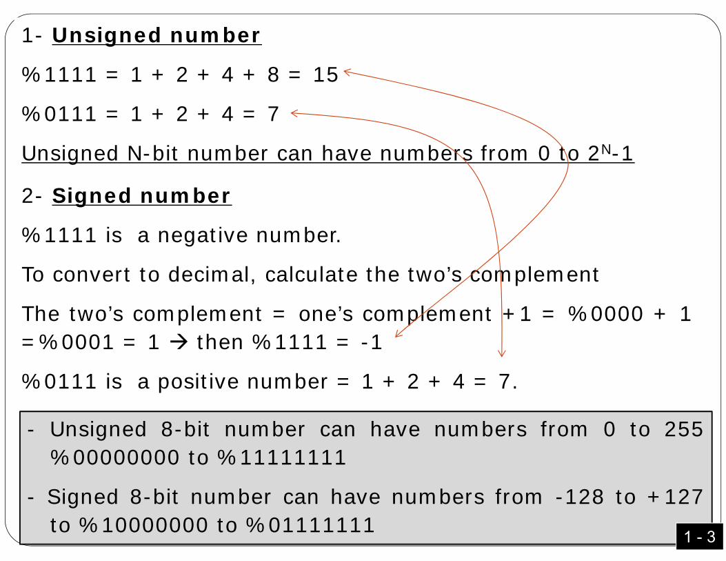
- Unsigned 8-bit number can have numbers from 0 to 255%00000000 to %11111111
- Signed 8-bit number can have numbers from -128 to +127to %10000000 to %01111111 1 - 3
1- Unsigned number
%1111 = 1 + 2 + 4 + 8 = 15
%0111 = 1 + 2 + 4 = 7
Unsigned N-bit number can have numbers from 0 to 2N-1
2- Signed number
%1111 is a negative number.
To convert to decimal, calculate the two’s complement
The two’s complement = one’s complement +1 = %0000 + 1=%0001 = 1 then %1111 = -1
%0111 is a positive number = 1 + 2 + 4 = 7.

- Signed N-bit number can have numbers from -2N-1 to 2N-1-1- Unsigned 3-bit number can represent numbers from 0 (=
%000) to 7 (=111)- Signed 3-bit number can represent numbers from -4 (= %100)
to 3 (= %011)
1 - 4
Computer does not know whether a bit sequence represents a signed or an unsigned number ->It is the programmer’s responsibility!
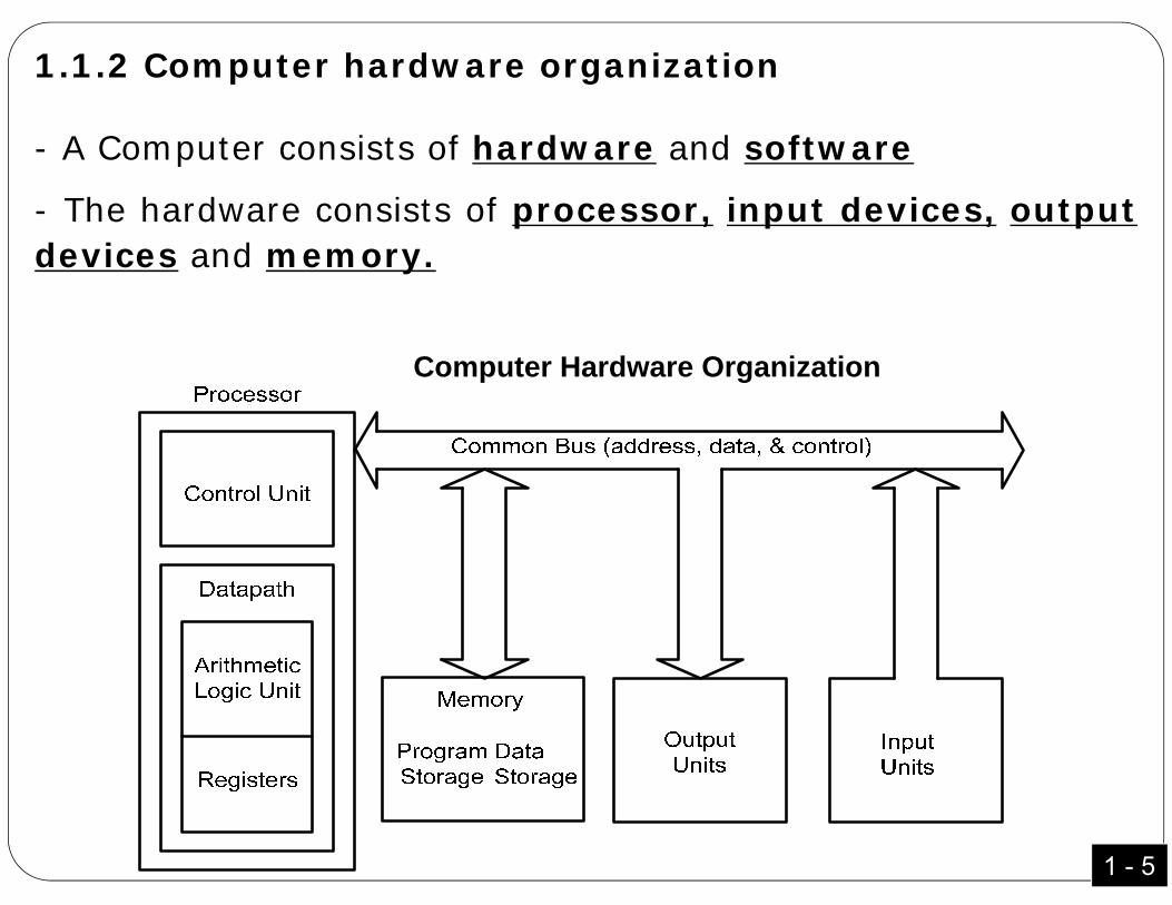
1.1.2 Computer hardware organization
- A Computer consists of hardware and software
- The hardware consists of processor, input devices, outputdevices and memory.
Computer Hardware Organization
1 - 5

1- Processor
- Also called Microprocessor (MP) or Central Processing Unit(CPU).
- Executes programs.
- Performs: (1) all of the computational operations and (2) thecoordination of the usage of resources of a computer
- Ex. can a memory and an input device write data on ashared bus simultaneously? NO, control signals are issuedby processor to coordinate the devices operations.
2- Input devices
- Used to enter the programs to be executed and the data tobe processed into the computer.
- Examples: keyboard, keypad, switches, sensors, scanners,bar code readers, etc.
1 - 6

3- Output devices
- The results of the operations done by the processor should bedisplayed or printed on a media so that the user can see them.
- Examples: seven segment displays, light emitting diode(LED), liquid crystal displays (LCD), a monitor, etc.
4- Memory
- Programs to be executed and data to be processed are storedin memory so that the processor can readily access them.
5- Buses
- Address bus: The set of conductor wires that carry addresssignals.
- Data bus: The set of conductor wires that carry data signals
- Control bus: The set of conductor wires that carry controlsignals
1 - 7

Outline
1.1 Computer hardware organization
1.2 The processor
1.3 Memory system operation
1.4 Program Execution
1.5 HCS12 Microcontroller

- A processor consists of arithmetic logic unit (ALU),control unit, and registers.
- The ALU performs the arithmetic and logic operationsrequested by the program.
- A simple ALU that can perform only four operations (addition,summation, AND, OR) is shown in Figure 1.1.
1 - 8

- All four operations are performed simultaneously by differentcircuits whereas the instruction opcode tells the multiplexer toselect one of the four units’ outputs as the result
- The adder is used to perform addition and subtractionoperations
- The ALU is more complicated if the processor designer wantsto implement more operations directly in the hardware.
1 - 9I311
Select Output000110
I0
I1
I2
Remember how multiplexer works:
MUX output
I0
I1I2
I3
Inputs
Selector

The ALU operations:-
1- Opcode = 00
- The comparator output = 0, MUX2 output = CIN, MUX1 output =B, the adder inputs are n-bit A and n-bit B.
- The result of the adder is A + B + CIN, CIN is the input carry.
- MUX3 selects the output of the adder and the carry.
1 - 10
00
A + B+ CIN
0
0

1 - 11
01
A + B’ + 1= A - B
1
1
2- Opcode = 01
- The comparator output = 1, MUX2 output = 1, MUX1 output =B’ (one’ complement of B), the adder inputs are n-bit A and n-bit B’.
- The result of the adder is A + B’ + 1 = A - B. Remember B’ + 1= - B. B’ + 1 is the two’s complement of B.
- MUX3 selects the output of the adder and the carry (calledborrow).
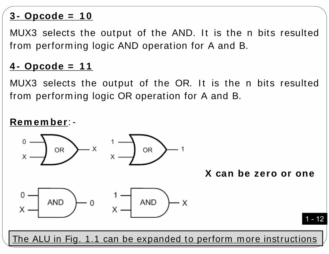
3- Opcode = 10
MUX3 selects the output of the AND. It is the n bits resultedfrom performing logic AND operation for A and B.
4- Opcode = 11
MUX3 selects the output of the OR. It is the n bits resultedfrom performing logic OR operation for A and B.
Remember:-
X can be zero or one
1 - 12
The ALU in Fig. 1.1 can be expanded to perform more instructions

2- Control Unit
- The control unit decodes machine codes and performs theoperations specified by them.
- A machine instruction has a mandated field called the opcodewhich can tell what operations are needed to execute theinstruction. Other fields are optional and used to specify theoperands to be operated on.
1 - 13
- A machine instruction is a combination of 0sand 1s.
- Instruction execution is timed by a clocksignal. A clock signal is a square signal. Ateach cycle, some operations are performed.
- A program usually has multiple instructionsthat are normally stored in sequentiallocations in memory.

- A program counter (PC) is used to keep track of the address ofthe instruction to be executed next.
- The first step to execute an instruction is to fetch it from thememory location pointed by PC and place it in the instructionregister (IR) where it is decoded, and executed.
- The result of the decoding process is appropriate control signalsto execute the instruction.
- Whenever the processor fetches an instruction, the PC will beincremented by the length of that instruction so that it points tothe next instruction.
- Both PC and IR are two registers inside the microprocessor.
- The processor may not execute instructions in sequence due tothe need to execute instructions based on the condition or theneed to repeat a certain group of instructions.
- The processor uses conditional and unconditional branch (orjump) instructions to change the program flow.
1 - 14

- Conditional branches are performed when a condition is satisfied,e.g., the previous instruction caused a carry.
- After executing an instruction, the condition code register(CCR) is usually automatically updated to reflect the result ofthe instruction.
- The CCR is usually used to make a condition in conditionalbranch. Each bit in the register is independent and has adifferent indication.
- Example, a zero flag bit is set if the instruction result is zero, asign flag bit is 1 if the result is negative and so on.
- EX.: A = A – BIf zero flag = 1 jump to --- 1 - 15
jump if A = B

3- Registers
- A register is a storage location inside the CPU.
- A register is used to hold data or address during the executionof an instruction.
- A register, very close to the ALU, provides fast access tooperands for program execution.
- The number of registers varies from processor to processor
- Unlike memory, registers are not used to store the program orlarge data.
- Accessing memory is much slower than accessing registers
1 - 16

2- Computer software
- Computer programs are known as software
- A program is a sequence of instructions
- Machine instruction: A sequence of binary digits which can beexecuted by the processor
0001 1000 0000 0110: A [A] + [B]0100 0011: A [A] + 1
- Machine instruction: Hard to understand, enter, debug, andmaintain for human being
- Assembly language: An assembly instruction is a mnemonicrepresentation of a machine instruction.
Examples: ABA ; A [A] + [B]
DECA ; A [A] – 1
1 - 17

1 - 18
- Assembler: A program that translates an assembly languageprogram to the equivalent machine code that can be executedby the microprocessor.
- Compiler: A program that translates a high level programminglanguage to the equivalent machine code.
- Source code: A program written in assembly or high-levellanguage

Compiler vs assembler
- Compiler is more complex than assembler
- Each assembly language instruction is translated to one machinelanguage instruction
- But, one statement written in high level language may betranslated into tens or hundreds of machine languageinstructions and this translation is not usually optimal
- Assembly language uses mnemonic symbol to represent eachmachine translation
- Using symbols can make programming much easier than usingbinary machine codes
- The microprocessor can execute only machine languageinstructions 1 - 19

Microprocessor VS Microcontroller
- A microprocessor (MP) needs external devices such asmemory, I/O ports, etc to run a program.
- A microcontroller (MCU) contains a microprocessor, memoryand I/O ports within a single chip.
- It may also contain timer, serial communication interface,and A/D (analog/digital) and D/A converters
- Microcontrollers have been used in almost every product thatrequires a certain amount of intelligence.
- Microcontrollers have been used in printers, modems, MP3players, cars, home appliances such as washing machines,microwave ovens, etc.
1 - 20

1 - 21
Embedded Systems
- An embedded system is a special purpose computer systemdesigned to perform a dedicated function.
- Software written for embedded systems is often calledfirmware and is stored in flash memory chips.
- Examples of embedded systems: MP3 players, traffic lights,digital watches

Outline
1.1 Computer hardware organization
1.2 The processor
1.3 Memory system operation
1.4 Program Execution
1.5 HCS12 Microcontroller

Semiconductor Memory
- Widely used in embedded systems.
- Non-volatile memory does not lose the information whenthere is no power, but volatile memory does.
- Read only memory: the MP can read but cannot write.
- Reading memory is nondestructive – memory does not losedata when CPU reads.
- Writing memory is destructive – when the CPU writes data tomemory, the old data is written over and destroyed.
1- Random Access Memory (RAM)
- Read/write by MP.
- Same amount of time is required to access any location onthe same chip.
- Dynamic random access memory (DRAM), and Static randomaccess memory (SRAM) are volatile. 1 - 22

- Magneto RAM (MRAM) and Ferroelectric RAM (FRAM) arenon-volatile.
2- Read-only memory (ROM):
- Nonvolatile.
- Mask-Programmed ROM (MROM) is programmed once duringmanufacture.
- Programmable read-only memory (PROM): programmedonce by the end user by using a special device.
- Erasable programmable ROM (EPROM): Electricallyprogrammable many times by user by using a special device.The whole chip can be erased by ultraviolet light.
- Electrically erasable programmable ROM (EEPROM):Electrically Programmable many times by user by using aspecial device. Electrically erasable by using a special device.can be erased one location, one row, or whole chip in oneoperation 1 - 23

Flash memory:
- Electrically erasable and programmable many times by theMP.
- Can erase a block or the whole chip.
- The most widely used nonvolatile memory technology.
- Most microcontrollers use on-chip flash memory as theirprogram memory.
1 - 24

Memory System Operation
- Each memory location has two components: address andcontents.
- The organization of a memory chip is indicated by m x n,where m is the number of locations in the chip and n indicatesthe number of bits in one location.
- The number of address bits needed for selecting a memorylocation is Log2m
- For example a memory chip has 16 bits addressing bits, howmany locations are in this memory? 216 = 64 Kbytes
- How many addressing bits are needed to point to 64 Kbyteslocations? Log264K = 16 bits
- The memory data bits are connected to the data bus.
- The memory address bits are connected to the address bus.1 - 25

- Registers are referred to by their names whereas memorylocations are referred to by their addresses
Byte = 8 bits, Word = 2 bytes = 16 bits, Nibble = 4 bits
Kilobyte (KB) = 210 bytes =1026 bytes
Megabyte (MB) = K2 Bytes = 220 bytes = 1,048,576 bytes
Gigabyte (GB) = K3 Bytes = 230 bytes = 1,073,741,824 bytes
1 - 26

Read Operation
- RD (Read) in the MP is connected to OE (output enable) in thememory and WR (write) is connected to WE (write enable)
- The processor places the address of the memory location that itintends to read on the address bus and asserts the RD signal.(RD = 1 and WR = 0)
- After some time, the data stored in the location referred by theaddress will be out of the memory to the data bus to be read bythe MP.
- RD and WR are two control signals to inform the memory toread or write.
1 - 27
m = 2d locations
d bitsn bits
n bits
Write Operation
- The processor places the address of the location that itintends to write on the address bus.
- The processor also places the data that it intends to write onthe data bus and asserts the WE signal (RD = 0 and WR =1)
- The memory chip stores the data on the data bus in theselected memory location after some time.
- If a memory location is one byte but we want to store largerdata, e.g., 16-bit number what should we do?
Store the data in two locations. To read the data, we read twolocations and to write, we write two times.
- RD and WR can not be 1 at the same time but can bezeroes. Only one operation can be done at a time.
1 - 28

Outline
1.1 Computer hardware organization
1.2 The processor
1.3 Memory system operation
1.4 Program Execution
1.5 HCS12 Microcontroller

- In embedded systems, the program is stored in a nonvolatilememory.
- Where does the processor start to execute program after poweron?
(1) From a fixed location such as address 0 (Atmelmicrocontroller), or (2) Fetch the starting address from a fixedlocation in the memory ($FFFE and $FFFF in HCS12)
- How does the processor update the program counter (PC)?Increment PC by the length of the instruction just executed.
- How flow control instructions (such as Jump) are executed? Setthe PC with the address of the target instruction.
- Flip-flop can store one bit, e.g., D flip-flop
When set = 0, Q = 1 at the first rising edge clockWhen reset = 0, Q = 0 at the first rising edge clockOtherwise: Q = D at the first rising edge clock (CLK)
1 - 29

- The PC is 16-bit register having 16 flip-flops, each flip-flop storesone bit
- A common building block for the PC circuit is shown below.
1- Whenever the power is turned on, the flip-flops are reset, PC =$0000 and the instruction at address $0000 is the first to beexecuted.
1 - 30
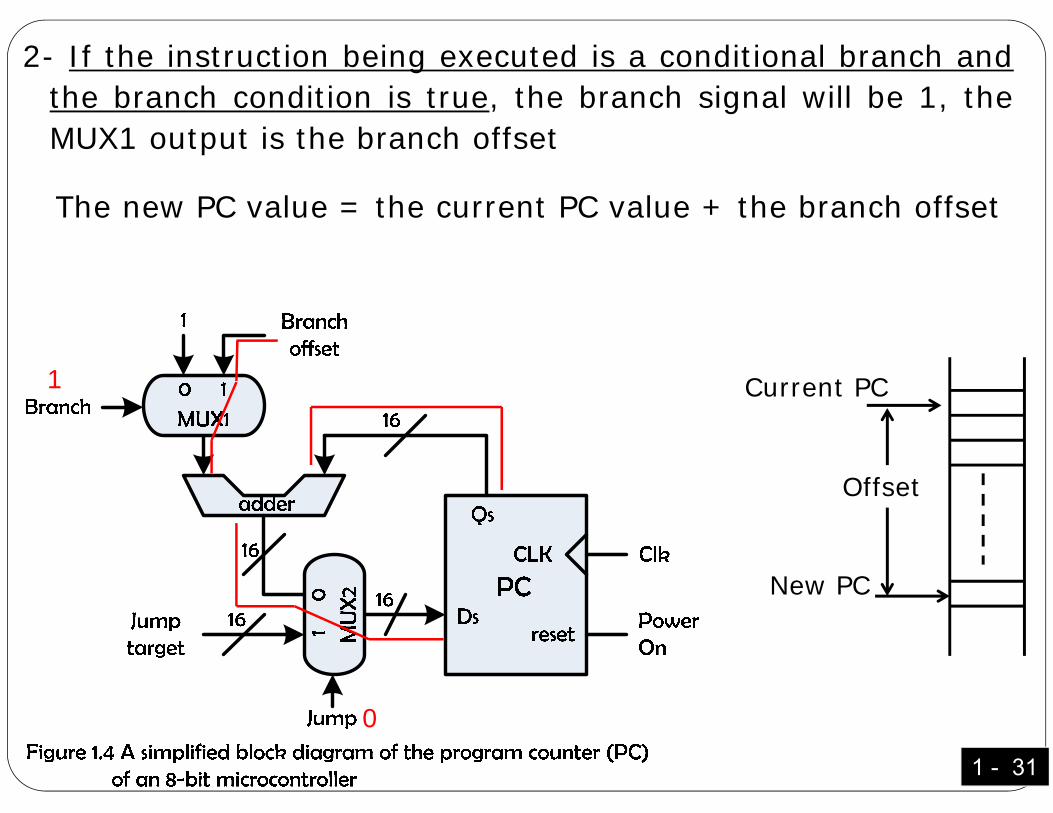
2- If the instruction being executed is a conditional branch andthe branch condition is true, the branch signal will be 1, theMUX1 output is the branch offset
The new PC value = the current PC value + the branch offset
1 - 31
1
0
Current PC
New PC
Offset

3- If the instruction being executed is a jump instruction, thenPC = Jump target (or the target address)
- In Jump instruction, there is no condition and the jump isalways taken.
1 - 32
1
Current PC
$3000
To jump to the instruction at $3000, PC = $3000

3- If the instruction being executed is not a program flowcontrol instruction, then
The new PC value = the old PC value + the instruction’snumber of bytes
PC is incremented by 1 after each instruction byte is fetched.
1 - 33
0
0

$0000
1 - 34
Executing a program
ld 0x20, #0ld 0x21, #20ld ptr, #0x2000loop: ld A,@ptrand A, #0x03bnz nextinc 0x20next: dbnz 0x21,loop
1- The assembler converts the assembly program to machine code and stores it in the memory starting from $0000.
1 - 35
2- Each time the microcontroller is reset, it starts executing from location $0000 that means PC should be $0000
3- Two phases to execute an instruction:-
3.1 Instruction fetch:
- Read the instruction from the memory and store it in the instruction register (IR)
- May need more than one reading operation if the instruction is more than one byte.
- Update PC to point at the next instruction. How? Increment PC each time a byte of the instruction is read
3.2 Instruction Execution
- The control unit decodes the instruction and issues appropriatecontrol signals to execute it.
- It may need to read/write the memory.

1 - 36
Instruction ld $20,#0 (machine code 75 20 00)
Place 0 in data memory at 0x20
1- Fetch instruction:
- The Processor places contents of PC (0) on the address bus toread the instruction to be executed.
-It reads the first byte (opcode) = $75. PC is incremented to$0001.
-From the opcode, the control unit recognizes that it needs to readthe following two bytes after the opcode. It reads $20 and $00 andholds them in IR. PC is incremented after each read operation tobe 3 to point at the next executed instruction.
2- Execute the instruction:
- Address bus ← $20 and Data bus ← $00
- WR =1 to write 0 into the memory location $20.

Executing this instruction does not change PC, but jump instruction does. 1 - 37
Initially PC = 0
PC = PC +1 after reading the byte pointed by 0 (or 75)

Instruction ld $21,#$14 (machine code 75 21 14)
- Similar to previous instruction.- PC = 0x0006 and write $14 to memory location $20.
-------------------------------------------------------
Instruction ld ptr,#$2000 (machine code 90 20 00)
- Load $2000 into the ptr register
1- Fetch instruction:- The address bus ← PC value (0x06), request to read.- Opcode = $90 and PC = $07.- From the opcode, we need to read the following two
locations. Read $20 and $00 and PC = 0x09.
2- Execute instruction:ptr ← 2000
1 - 38

1 - 39
The machine code of the program
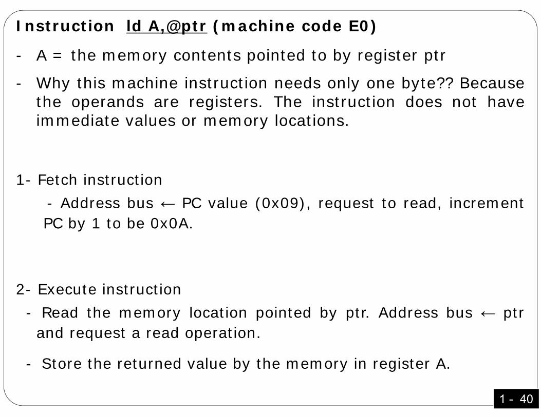
Instruction ld A,@ptr (machine code E0)
- A = the memory contents pointed to by register ptr
- Why this machine instruction needs only one byte?? Becausethe operands are registers. The instruction does not haveimmediate values or memory locations.
1- Fetch instruction- Address bus ← PC value (0x09), request to read, incrementPC by 1 to be 0x0A.
2- Execute instruction- Read the memory location pointed by ptr. Address bus ← ptrand request a read operation.
- Store the returned value by the memory in register A.
1 - 40

Instruction and A,#$03 (machine code 54 03)
- And the value 0x03 with accumulator A
1- Fetch instruction- Reading two bytes and update PC to $0C.
2- Execute instruction
- Perform an AND operation on the contents of A and thevalue 0x03 and store the result in A
1 - 41

Notice: Some instructions takes more execution time because they do more operations. Usually the instructions that need memory read/write takes more time.
Instruction bnz next (machine code is 70 02)
- Branch if the result of the last operation is not 0
1- Fetch instruction
- Read two bytes where 02 is the branch offset. PC is updatedto 0x0E.
2- Execute instruction
- If the result of the last instruction is zero, PC = PC + 02,(the jump is taken)
- Else does nothing because PC points at the followinginstruction – the branch should not be take.
1 - 42

Instruction inc $20 (machine code 05 20)
- Increment the memory location at $20 by 1
1- Fetch instruction
- Read two bytes PC is updated to $10F.
2- Execute instruction
- Read the content of the memory location $20 and store in aMDR register.
- Add one to the MDR register.
- Store MDR in memory location $20: address bus ← $20, databus ← content of MDR, and requests write operation.
1 - 43

Outline
1.1 Computer hardware organization
1.2 The processor
1.3 Memory system operation
1.4 Program Execution
1.5 HCS12 Microcontroller

The HCS12 Features
- 16-bit CPU (the operations can be done on 16 bit data)
- Maximum operating clock frequency 25 MHz
- 0 KB to 4KB of on-chip EEPROM
- 2KB to 14KB of on-chip SRAM
- 32 KB to 512KB on-chip flash memory
- Timer
- Serial communication interfaces
- 10-bit A/D converter
- I/O pins to interface to I/O devices
1 - 44

Two types of registers:-1- CPU registers: used to perform general purpose operations such
as arithmetic, logic, and program flow control.2- I/O registers: used to configure the operations of the I/O
devices and to hold data transferred in and out of the devices- CPU registers do not occupy memory space.- I/O registers have addresses and are treated as memory
locations when they are accessed
CPU registers:- Some registers are 8 bits others are 16 bits.
1- General-purpose accumulators A and B- Both A and B are 8 bits.- Most arithmetic functions are done on them- A and B can be concatenated to form a single 16-bit registeraccumulator referred as the D accumulator
1 - 45

The HCS12 CPU Registers
7 00 7A B
15 0D
8-bit accumulator A and Bor16-bit double accumulator D
15 0X
15 0Y
Index register X
Index register Y
15 0SP Stack pointer
15 0PC Program counter
Condition code register
CarryOverflowZeroNegativeI Interrupt maskHalf-Carry (from bit 3)X Interrupt MaskStop Disable
Figure 1.10 HCS12 CPU registers.
S X H I N Z V C
1 - 46

When A changes B is unaffected and vice versa, but when Dchanges both A and B change.
2- Index registers X and Y: 16 bits. Used to hold addresses. Theyare also used in several arithmetic instructions.
3- Stack pointer (SP): 16 bits. A stack is a first-in-first-out datastructure. SP points to the top byte of the stack as shown infigure.
4- Program counter (PC): 16 bits holds the address of the nextinstruction to be executed.
Lower address
Higher address
Top of stack SP
Pop
Push5- Condition code register (CCR):
8-bit register used to
1- Flags are automatically updatedafter executing each instructionto reflect the status of the result.
2- Enable and disable interrupts1 - 47

Questions
Mohamed Mahmoud