Microprocessor Architecture - WBUTHELP.COM · Microprocessor Architecture • The microprocessor...
46
Microprocessor Architecture mywbut.com 1
Transcript of Microprocessor Architecture - WBUTHELP.COM · Microprocessor Architecture • The microprocessor...
Microprocessor Architecture
mywbut.com 1
Microprocessor Architecture• The microprocessor can be programmed to
perform functions on given data by writing specific instructions into its memory.– The microprocessor reads one instruction at a
time, matches it with its instruction set, and performs the data manipulation specified.
– The result is either stored back into memory or displayed on an output device.
mywbut.com 2
The 8085 Architecture• The 8085 uses three separate busses to perform
its operations– The address bus.– The data bus.– The control bus.
mywbut.com 3
The Address Bus– 16 bits wide (A0 A1…A15)
• Therefore, the 8085 can access locations with numbers from 0 to 65,536. Or, the 8085 can access a total of 64K addresses.
– “Unidirectional”.• Information flows out of the microprocessor and into the
memory or peripherals.
– When the 8085 wants to access a peripheral or a memory location, it places the 16-bit address on the address bus and then sends the appropriate control signals.
mywbut.com 4
The Data Bus– 8 bits wide (D0 D1…D7)– “Bi-directional”.
• Information flows both ways between the microprocessor and memory or I/O.
– The 8085 uses the data bus to transfer the binary information.
– Since the data bus has 8-bits only, then the 8085 can manipulate data 8 bits at-a-time only.
mywbut.com 5
The Control Bus– There is no real control bus. Instead, the control
bus is made up of a number of single bit control signals.
mywbut.com 6
Operation Types in a Microprocessor• All of the operations of the microprocessor can
be classified into one of three types:- Microprocessor Initiated Operations- Internal Operations- Peripheral Initiated Operations
mywbut.com 7
Microprocessor Initiated Operations• These are operations that the microprocessor
itself starts.• These are usually one of 4 operations:
– Memory Read– Memory Write– I/O Read (Get data from an input device)– I/O write (Send data to an output device)
mywbut.com 8
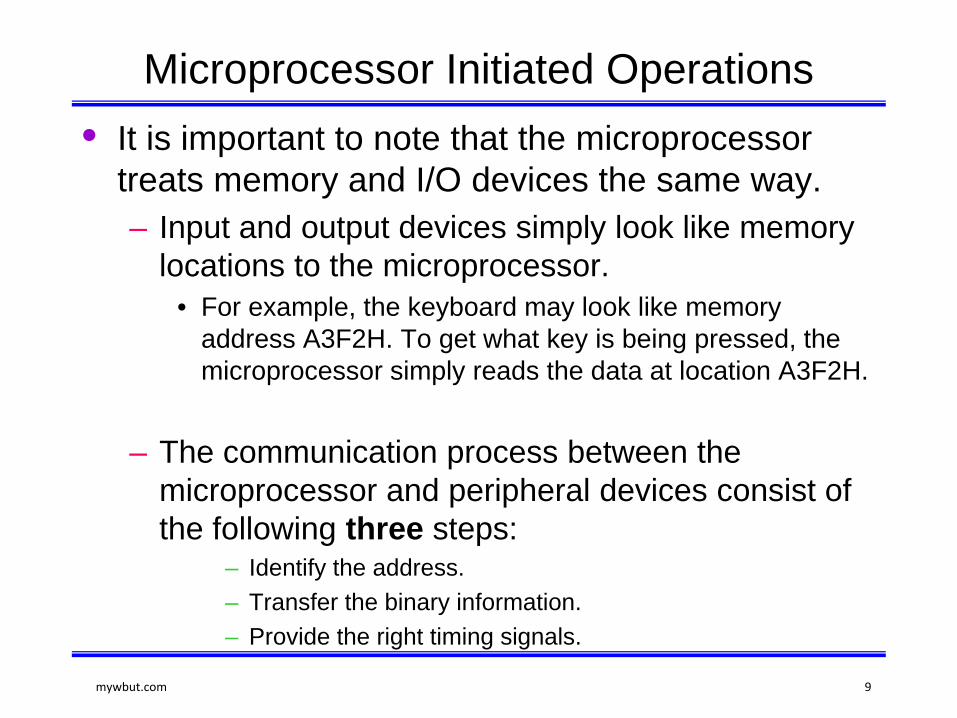
Microprocessor Initiated Operations• It is important to note that the microprocessor
treats memory and I/O devices the same way. – Input and output devices simply look like memory
locations to the microprocessor.• For example, the keyboard may look like memory
address A3F2H. To get what key is being pressed, the microprocessor simply reads the data at location A3F2H.
– The communication process between the microprocessor and peripheral devices consist of the following three steps:
– Identify the address.– Transfer the binary information.– Provide the right timing signals.
mywbut.com 9
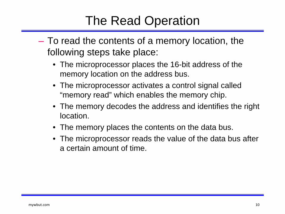
The Read Operation– To read the contents of a memory location, the
following steps take place:• The microprocessor places the 16-bit address of the
memory location on the address bus. • The microprocessor activates a control signal called
“memory read” which enables the memory chip.• The memory decodes the address and identifies the right
location. • The memory places the contents on the data bus. • The microprocessor reads the value of the data bus after
a certain amount of time.
mywbut.com 10
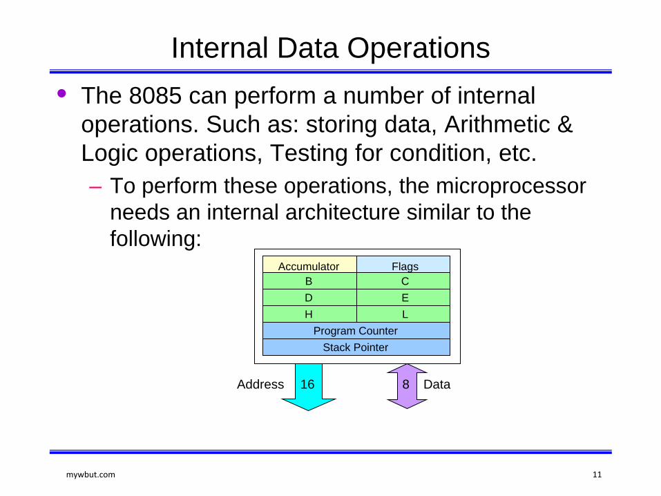
Internal Data Operations• The 8085 can perform a number of internal
operations. Such as: storing data, Arithmetic & Logic operations, Testing for condition, etc.– To perform these operations, the microprocessor
needs an internal architecture similar to the following:
Accumulator FlagsB CD EH L
Program CounterStack Pointer
DataAddress 816
mywbut.com 11
The Internal Architecture• We have already discussed the general purpose
registers, the Accumulator, and the flags.
• The Program Counter (PC)– This is a register that is used to control the
sequencing of the execution of instructions.– This register always holds the address of the next
instruction.– Since it holds an address, it must be 16 bits wide.
mywbut.com 12
The Internal Architecture• The Stack pointer
– The stack pointer is also a 16-bit register that is used to point into memory.
– The memory this register points to is a special area called the stack.
– The stack is an area of memory used to hold data that will be retreived soon.
– The stack is usually accessed in a Last In First Out (LIFO) fashion.
mywbut.com 13
Externally Initiated Operations• External devices can initiate (start) one of the 4
following operations:– Reset
• All operations are stopped and the program counter is reset to 0000.
– Interrupt• The microprocessor’s operations are interrupted and the
microprocessor executes what is called a “service routine”.
• This routine “handles” the interrupt, (perform the necessary operations). Then the microprocessor returns to its previous operations and continues.
mywbut.com 14
Externally Initiated Operations– Ready
• The 8085 has a pin called RDY. This pin is used by external devices to stop the 8085 until they catch up.
• As long as the RDY pin is low, the 8085 will be in a wait state.
– Hold• The 8085 has a pin called HOLD. This pin is used by
external devices to gain control of the busses.• When the HOLD signal is activated by an external
device, the 8085 stops executing instructions and stops using the busses.
• This would allow external devices to control the information on the busses. Example DMA.
mywbut.com 15
The Design and Operation of Memory• Memory in a microprocessor system is where
information (data and instructions) is kept. It can be classified into two main types:
• Main memory (RAM and ROM) • Storage memory (Disks , CD ROMs, etc.)
– The simple view of RAM is that it is made up of registers that are made up of flip-flops (or memory elements).
• The number of flip-flops in a “memory register” determines the size of the memory word.
– ROM on the other hand uses diodes instead of the flip-flops to permanently hold the information.
mywbut.com 16
Accessing Information in Memory• For the microprocessor to access (Read or Write)
information in memory (RAM or ROM), it needs to do the following:– Select the right memory chip (using part of the
address bus).– Identify the memory location (using the rest of the
address bus).– Access the data (using the data bus).
mywbut.com 17
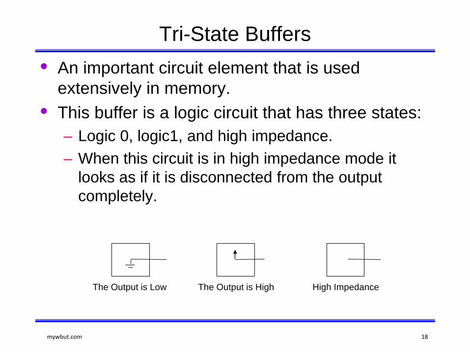
Tri-State Buffers• An important circuit element that is used
extensively in memory.• This buffer is a logic circuit that has three states:
– Logic 0, logic1, and high impedance.– When this circuit is in high impedance mode it
looks as if it is disconnected from the output completely.
The Output is Low The Output is High High Impedance
mywbut.com 18
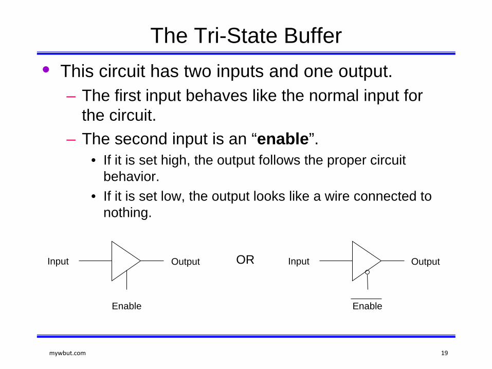
The Tri-State Buffer• This circuit has two inputs and one output.
– The first input behaves like the normal input for the circuit.
– The second input is an “enable”.• If it is set high, the output follows the proper circuit
behavior.• If it is set low, the output looks like a wire connected to
nothing.
Input Output
Enable
Input Output
Enable
OR
mywbut.com 19
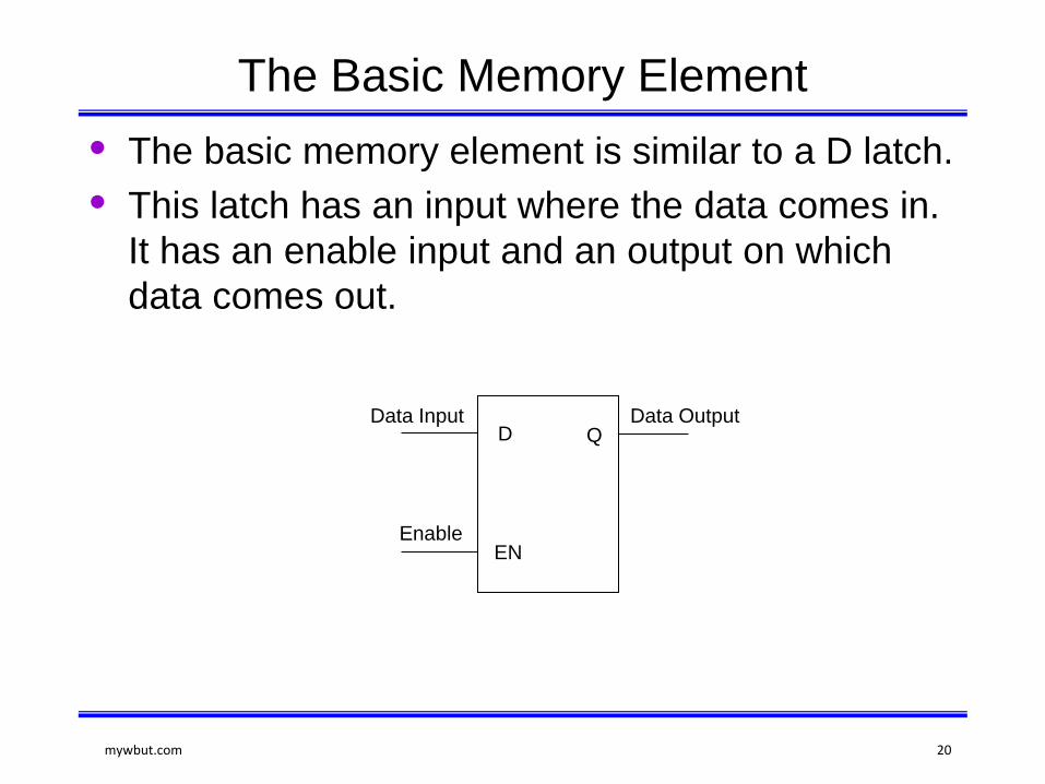
The Basic Memory Element• The basic memory element is similar to a D latch.• This latch has an input where the data comes in.
It has an enable input and an output on which data comes out.
QD
EN
Data Input Data Output
Enable
mywbut.com 20
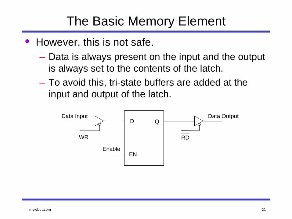
The Basic Memory Element• However, this is not safe.
– Data is always present on the input and the output is always set to the contents of the latch.
– To avoid this, tri-state buffers are added at the input and output of the latch.
QD
EN
Data Input Data Output
Enable
WR RD
mywbut.com 21
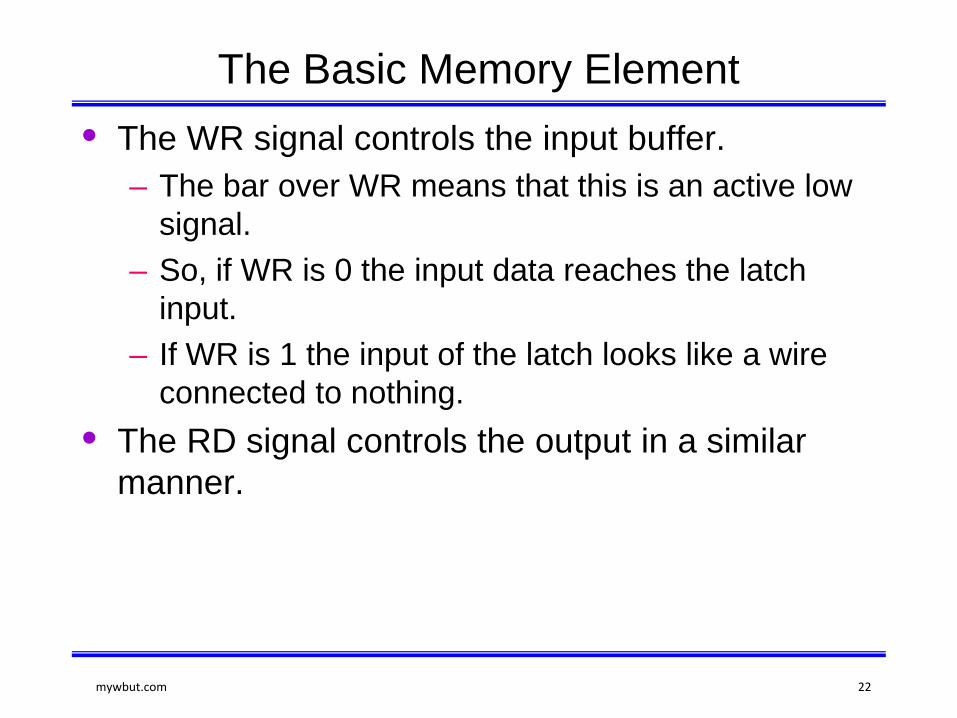
The Basic Memory Element• The WR signal controls the input buffer.
– The bar over WR means that this is an active low signal.
– So, if WR is 0 the input data reaches the latch input.
– If WR is 1 the input of the latch looks like a wire connected to nothing.
• The RD signal controls the output in a similar manner.
mywbut.com 22
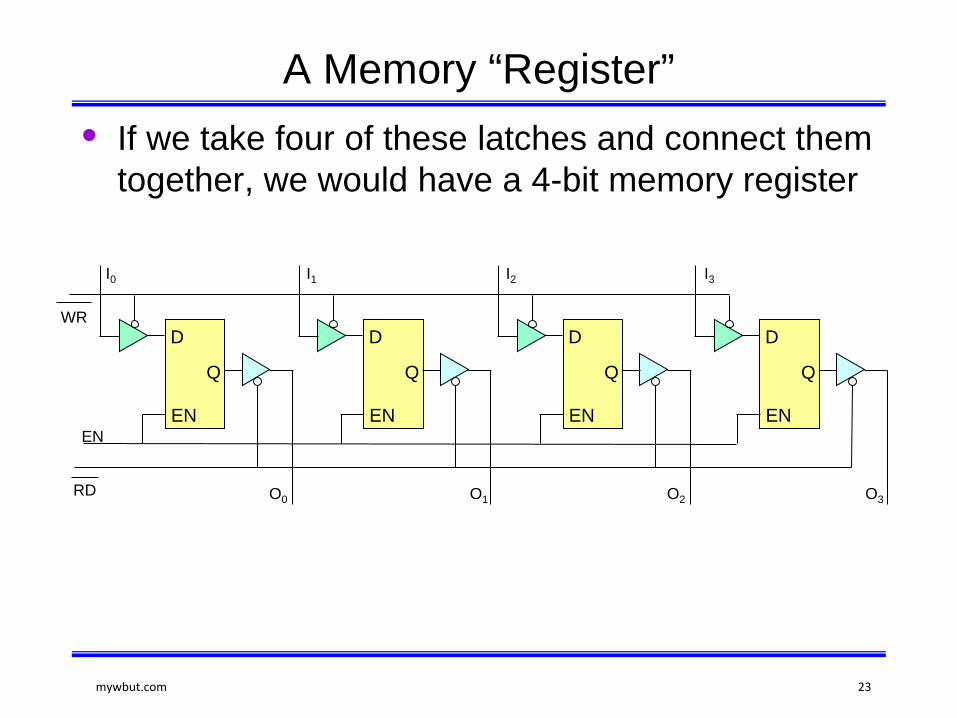
A Memory “Register”• If we take four of these latches and connect them
together, we would have a 4-bit memory register
WR
RD
EN
Q
D
EN
Q
D
EN
Q
D
EN
Q
D
EN
I0 I1 I2 I3
O0 O1 O2 O3
mywbut.com 23
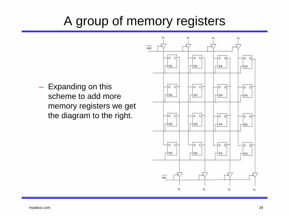
A group of memory registers
– Expanding on this scheme to add more memory registers we get the diagram to the right.
D
EN
Q D
EN
Q D
EN
Q D
EN
Q
D
EN
Q D
EN
Q D
EN
Q D
EN
Q
D
EN
Q D
EN
Q D
EN
Q D
EN
Q
D
EN
Q D
EN
Q D
EN
Q D
EN
Q
D0 D1 D2 D3
D0 D1 D2 D3
oooo
oooo
WR
RD
mywbut.com 24
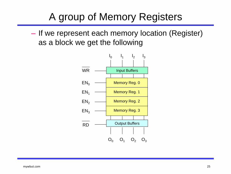
A group of Memory Registers– If we represent each memory location (Register)
as a block we get the following
Input Buffers
Output Buffers
Memory Reg. 0
Memory Reg. 1
Memory Reg. 2
Memory Reg. 3
I0 I1 I2 I3
O0 O1 O2 O3
WR
EN0
EN1
EN2
EN3
RD
mywbut.com 25
The Design of a Memory Chip• Using the RD and WR controls we can determine
the direction of flow either into or out of memory. Then using the appropriate Enable input we enable an individual memory register.
• What we have just designed is a memory with 4 locations and each location has 4 elements (bits). This memory would be called 4 X 4 [Number of location X number of bits per location].
mywbut.com 26
The Enable Inputs• How do we produce these enable line?
– Since we can never have more than one of these enables active at the same time, we can have them encoded to reduce the number of lines coming into the chip.
– These encoded lines are the address lines for memory.
mywbut.com 27
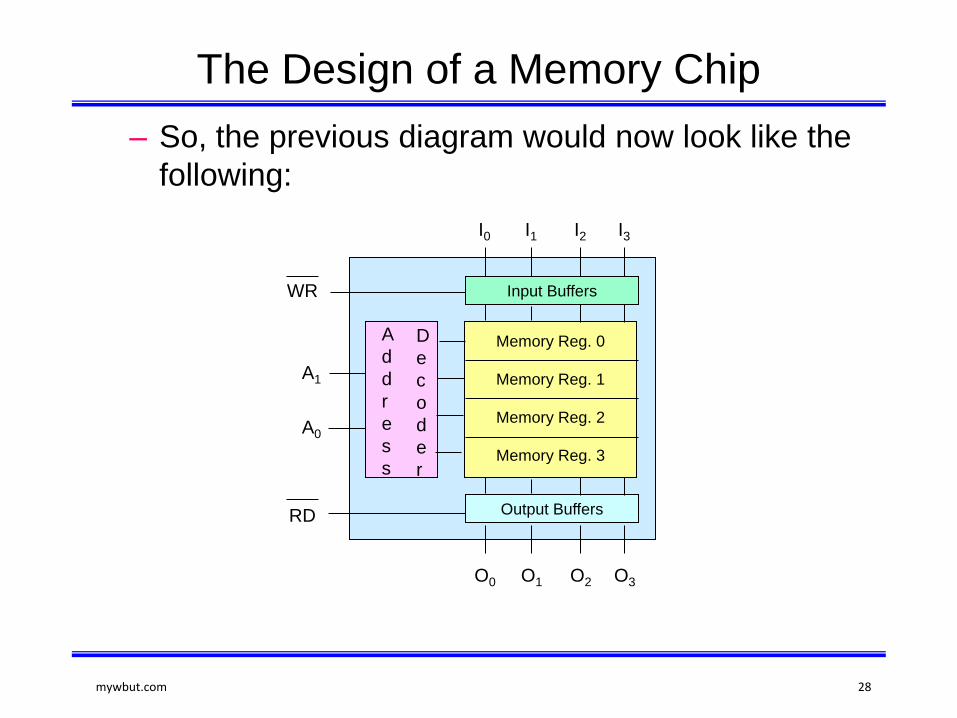
The Design of a Memory Chip– So, the previous diagram would now look like the
following:
Input Buffers
Output Buffers
Memory Reg. 0
Memory Reg. 1
Memory Reg. 2
Memory Reg. 3
I0 I1 I2 I3
O0 O1 O2 O3
WR
RD
Address
Decoder
A1
A0
mywbut.com 28
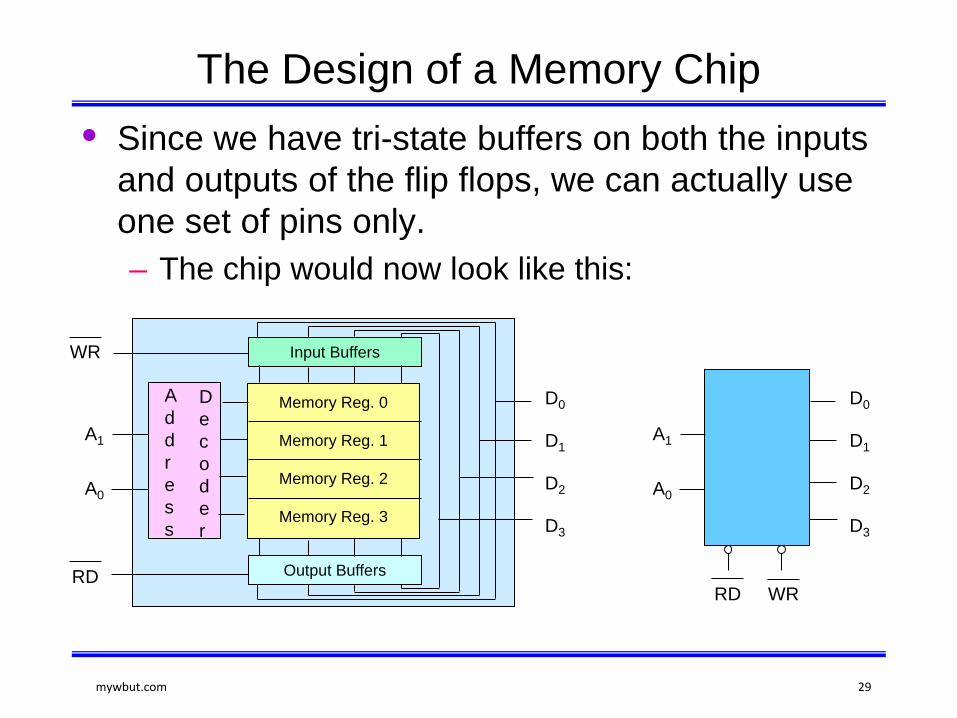
The Design of a Memory Chip• Since we have tri-state buffers on both the inputs
and outputs of the flip flops, we can actually use one set of pins only.– The chip would now look like this:
Input Buffers
Output Buffers
Memory Reg. 0
Memory Reg. 1
Memory Reg. 2
Memory Reg. 3
WR
RD
Address
Decoder
A1
A0
D0
D1
D2
D3
D0
D1
D2
D3
A1
A0
RD WR
mywbut.com 29
The steps of writing into Memory• What happens when the programmer issues the
STA instruction?– The microprocessor would turn on the WR control
(WR = 0) and turn off the RD control (RD = 1).– The address is applied to the address decoder
which generates a single Enable signal to turn on only one of the memory registers.
– The data is then applied on the data lines and it is stored into the enabled register.
mywbut.com 30
Dimensions of Memory• Memory is usually measured by two numbers: its
length and its width (Length X Width).• The length is the total number of locations.• The width is the number of bits in each location.
– The length (total number of locations) is a function of the number of address lines.
# of memory locations = 2( # of address lines)
• So, a memory chip with 10 address lines would have 210 = 1024 locations (1K)
• Looking at it from the other side, a memory chip with 4K locations would need
Log2 4096=12 address lines
mywbut.com 31
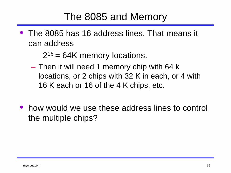
The 8085 and Memory• The 8085 has 16 address lines. That means it
can address 216 = 64K memory locations.
– Then it will need 1 memory chip with 64 k locations, or 2 chips with 32 K in each, or 4 with 16 K each or 16 of the 4 K chips, etc.
• how would we use these address lines to control the multiple chips?
mywbut.com 32
Chip Select• Usually, each memory chip has a CS (Chip
Select) input. The chip will only work if an active signal is applied on that input.
• To allow the use of multiple chips in the make up of memory, we need to use a number of the address lines for the purpose of “chip selection”.– These address lines are decoded to generate the
2n necessary CS inputs for the memory chips to be used.
mywbut.com 33
Chip Selection Example– Assume that we need to build a memory system
made up of 4 of the 4 X 4 memory chips we designed earlier.
– We will need to use 2 inputs and a decoder to identify which chip will be used at what time.
– The resulting design would now look like the one on the following slide.
mywbut.com 34
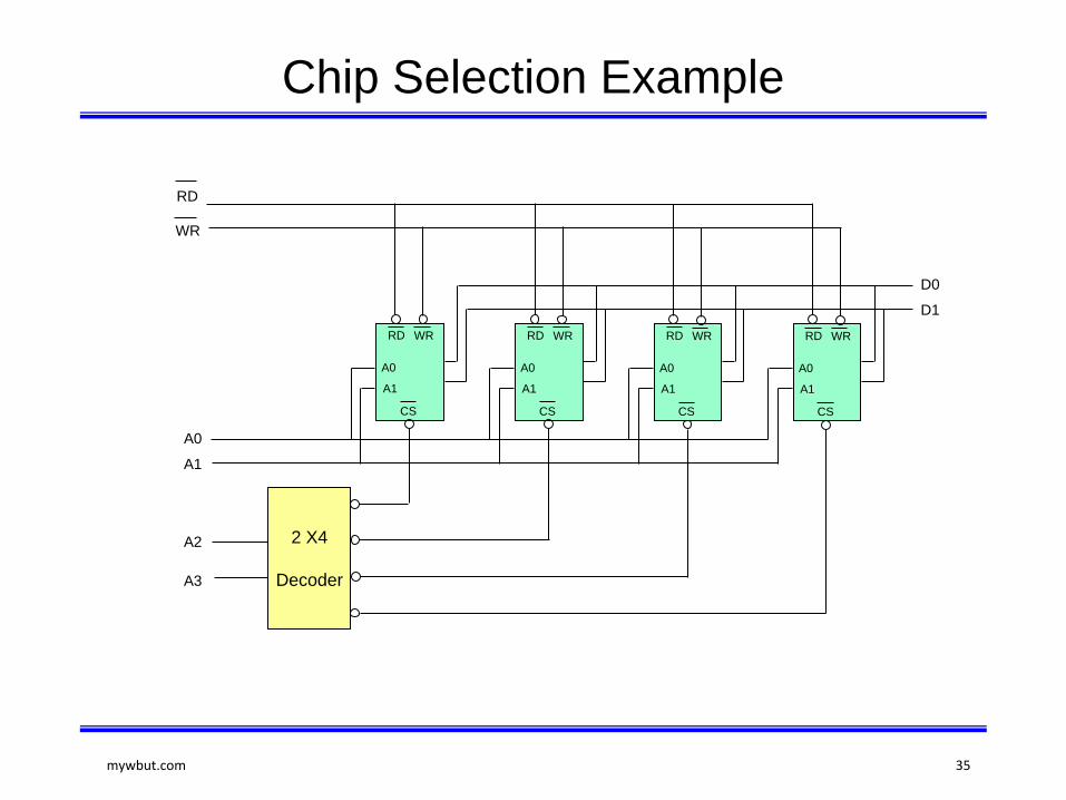
Chip Selection Example
CS
RD WR
A0
A1
CS
RD WR
A0
A1
CS
RD WR
A0
A1
CS
RD WR
A0
A1
2 X4
DecoderA3
A2
A1
A0
RD
WR
D1
D0
mywbut.com 35
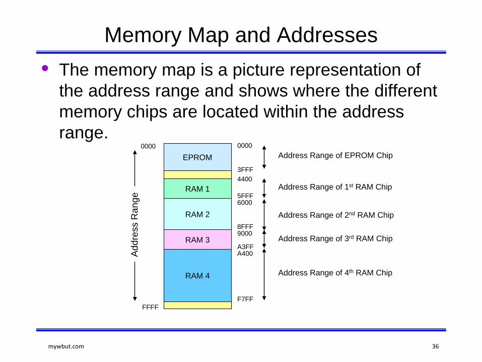
Memory Map and Addresses• The memory map is a picture representation of
the address range and shows where the different memory chips are located within the address range.
0000
FFFF
Addr
ess
Ran
ge
RAM 1
RAM 2
RAM 3
RAM 4
EPROM0000
3FFF4400
5FFF6000
8FFF9000
A3FFA400
F7FF
Address Range of EPROM Chip
Address Range of 1st RAM Chip
Address Range of 2nd RAM Chip
Address Range of 3rd RAM Chip
Address Range of 4th RAM Chip
mywbut.com 36
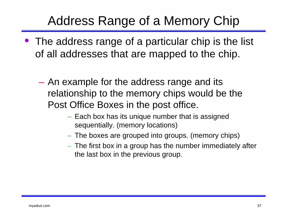
Address Range of a Memory Chip• The address range of a particular chip is the list
of all addresses that are mapped to the chip.
– An example for the address range and its relationship to the memory chips would be the Post Office Boxes in the post office.
– Each box has its unique number that is assigned sequentially. (memory locations)
– The boxes are grouped into groups. (memory chips)– The first box in a group has the number immediately after
the last box in the previous group.
mywbut.com 37
Address Range of a Memory Chip– The above example can be modified slightly to
make it closer to our discussion on memory.– Let’s say that this post office has only 1000 boxes. – Let’s also say that these are grouped into 10 groups of 100
boxes each. Boxes 0000 to 0099 are in group 0, boxes 0100 to 0199 are in group 1 and so on.
– We can look at the box number as if it is made up of two pieces:
– The group number and the box’s index within the group. – So, box number 436 is the 36th box in the 4th group.
The upper digit of the box number identifies the group and the lower two digits identify the box within the group.
mywbut.com 38
The 8085 and Address Ranges• The 8085 has 16 address lines. So, it can
address a total of 64K memory locations.– If we use memory chips with 1K locations each,
then we will need 64 such chips.– The 1K memory chip needs 10 address lines to
uniquely identify the 1K locations. (log21024 = 10)– That leaves 6 address lines which is the exact
number needed for selecting between the 64different chips (log264 = 6).
mywbut.com 39
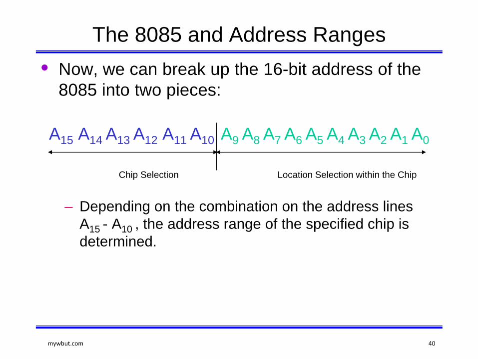
The 8085 and Address Ranges• Now, we can break up the 16-bit address of the
8085 into two pieces:
A15 A14 A13 A12 A11 A10 A9 A8 A7 A6 A5 A4 A3 A2 A1 A0
– Depending on the combination on the address lines A15 - A10 , the address range of the specified chip is determined.
Location Selection within the ChipChip Selection
mywbut.com 40
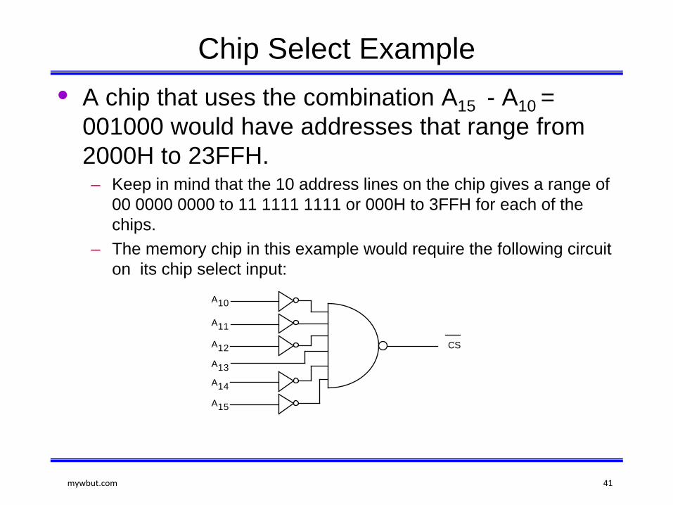
Chip Select Example• A chip that uses the combination A15 - A10 =
001000 would have addresses that range from 2000H to 23FFH.– Keep in mind that the 10 address lines on the chip gives a range of
00 0000 0000 to 11 1111 1111 or 000H to 3FFH for each of the chips.
– The memory chip in this example would require the following circuit on its chip select input:
CS
A10
A11
A12
A13A14
A15
mywbut.com 41
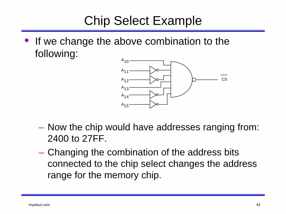
Chip Select Example• If we change the above combination to the
following:
– Now the chip would have addresses ranging from: 2400 to 27FF.
– Changing the combination of the address bits connected to the chip select changes the address range for the memory chip.
CS
A10
A11
A12A13A14
A15
mywbut.com 42
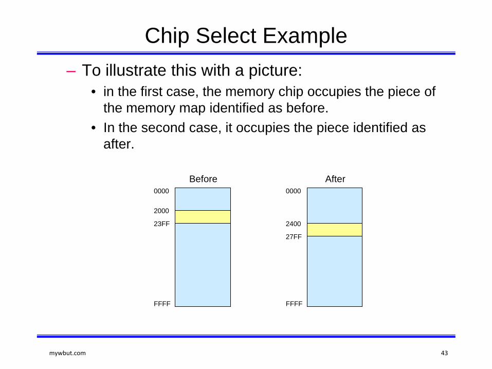
Chip Select Example– To illustrate this with a picture:
• in the first case, the memory chip occupies the piece of the memory map identified as before.
• In the second case, it occupies the piece identified as after.
0000
2000
23FF
FFFF
0000
2400
27FF
FFFF
Before After
mywbut.com 43
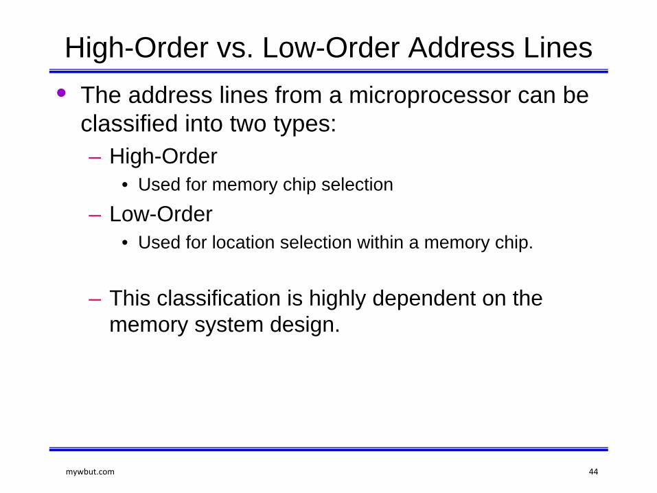
High-Order vs. Low-Order Address Lines• The address lines from a microprocessor can be
classified into two types:– High-Order
• Used for memory chip selection
– Low-Order• Used for location selection within a memory chip.
– This classification is highly dependent on the memory system design.
mywbut.com 44

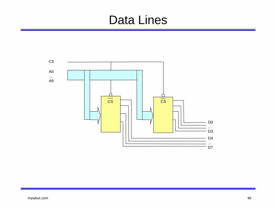
Data Lines• All of the above discussion has been regarding
memory length. Lets look at memory width. • We said that the width is the number of bits in
each memory word. – We have been assuming so far that our memory
chips have the right width. – What if they don’t?
• It is very common to find memory chips that have only 4 bits per location. How would you design a byte wide memory system using these chips?
• We use two chips for the same address range. One chip will supply 4 of the data bits per address and the other chip supply the other 4 data bits for the same address.
mywbut.com 45
Data Lines
CS
A0…A9
CS CS
D0…D3
D4…D7
mywbut.com 46