Chapter 1 Electrons and Holes in Semiconductors · PDF fileModern Semiconductor Devices for...
388
Modern Semiconductor Devices for Integrated Circuits (C. Hu) Slide 1-1 1.1 Silicon Crystal Structure • Unit cell of silicon crystal is cubic. • Each Si atom has 4 nearest neighbors. Chapter 1 Electrons and Holes in Semiconductors
Transcript of Chapter 1 Electrons and Holes in Semiconductors · PDF fileModern Semiconductor Devices for...

Modern Semiconductor Devices for Integrated Circuits (C. Hu) Slide 1-1
1.1 Silicon Crystal Structure
• Unit cell of silicon crystal is cubic.
• Each Si atom has 4 nearest neighbors.
Chapter 1 Electrons and Holes in Semiconductors

Modern Semiconductor Devices for Integrated Circuits (C. Hu) Slide 1-2
Silicon Wafers and Crystal Planes
•
Silicon wafers are usually cut along the (100) plane with a flat or notch to help orient the wafer during IC fabrication.
•
The standard notation for crystal planes is based on the cubic unit cell.
(100) (011) (111)
x
y y y
z z z
x x
Si (111) plane

Modern Semiconductor Devices for Integrated Circuits (C. Hu) Slide 1-3
1.2 Bond Model of Electrons and Holes • Silicon crystal in a two-dimensional
representation.
Si Si Si
Si Si Si
Si Si Si
• When an electron breaks loose and becomes a conduction electron , a hole is also created.
Si Si Si
Si Si Si
Si Si Si
Si Si Si
Si Si Si
Si Si Si

Modern Semiconductor Devices for Integrated Circuits (C. Hu) Slide 1-4
Dopants in Silicon
Si Si Si
Si Si
Si Si Si
Si Si Si
Si Si
Si Si Si
As B
• As, a Group V element, introduces conduction electrons and creates N-type silicon, • B, a Group III element, introduces holes and creates P-type silicon, and is called an acceptor. • Donors and acceptors are known as dopants. Dopant ionization energy ~50meV (very low).
and is called a donor.
Hydrogen: E ion m0 q4
13.6 eV = = 8ε0
2h2

Modern Semiconductor Devices for Integrated Circuits (C. Hu) Slide 1-5
GaAs, III-V Compound Semiconductors, and Their Dopants
As As Ga
Ga
• GaAs has the same crystal structure as Si. • GaAs, GaP, GaN are III-V compound semiconductors, important for optoelectronics. • Wich group of elements are candidates for donors? acceptors?
Ga As
As Ga Ga

Modern Semiconductor Devices for Integrated Circuits (C. Hu) Slide 1-6
1.3 Energy Band Model
• Energy states of Si atom (a) expand into energy bands of Si crystal (b). • The lower bands are filled and higher bands are empty in a semiconductor. • The highest filled band is the valence band. • The lowest empty band is the conduction band .
2p
2s
(a) (b)
conduction band)(
(valence band)
Filled lower bands
Empty upper bands

Modern Semiconductor Devices for Integrated Circuits (C. Hu) Slide 1-7
1.3.1 Energy Band Diagram
Conduction band E c
E v
E g
Band gap
Valence band
• Energy band diagram shows the bottom edge of conduction band, Ec , and top edge of valence band, Ev .
•
Ec and Ev are separated by the band gap energy, Eg .

Modern Semiconductor Devices for Integrated Circuits (C. Hu) Slide 1-8
Measuring the Band Gap Energy by Light Absorption
photons
photon energy: h v > E g
E c
E v
E g
electron
hole
Bandgap energies of selected semiconductors
• Eg can be determined from the minimum energy (hν) of photons that are absorbed by the semiconductor.
Semi-conductor InSb Ge Si GaAs GaP ZnSe Diamond
Eg (eV) 0.18 0.67 1.12 1.42 2.25 2.7 6

Modern Semiconductor Devices for Integrated Circuits (C. Hu) Slide 1-9
1.3.2 Donor and Acceptor in the Band Model
Conduction Band E c
E v Valence Band
Donor Level
Acceptor Level
E d
E a
Donor ionization energy
Acceptor ionization energy
Ionization energy of selected donors and acceptors in silicon
AcceptorsDopant Sb P As B Al In
Ionization energy, E c –E d or E a –E v (meV) 39 44 54 45 57 160
Donors

Modern Semiconductor Devices for Integrated Circuits (C. Hu) Slide 1-10
1.4 Semiconductors, Insulators, and Conductors
• Totally filled bands and totally empty bands do not allow
• Metal conduction band is half-filled.
E c
E v
E g = 1.1 eV
E c
E g = 9 eV empty
Si (Semiconductor) SiO 2
(Insulator) Conductor
E c filled
Top of conduction band
E v
current flow. (Just as there is no motion of liquid in a totally filled or totally empty bottle.) .
• Semiconductors have lower E g 's than insulators and can be
doped.

Modern Semiconductor Devices for Integrated Circuits (C. Hu) Slide 1-11
1.5 Electrons and Holes
• Both electrons and holes tend to seek their lowest
• Holes float up like bubbles in water . • Electrons tend to fall in the energy band diagram.
E c
E v
electron kinetic energy
hole kinetic energy
i n c r
e a s i
n g e
l e c t
r o n
e n e r
g y
i n c r
e a s i
n g h
o l e
e n e r
g y
energy positions.

The electron wave function is the solution of the three dimensional Schrodinger wave equation
Modern Semiconductor Devices for Integrated Circuits (C. Hu) Slide 1-12
ψψψ =+∇− )(2m
2
0
2
rV
The solution is of the form exp( k r) k = wave vector = 2π/electron wavelength
± ⋅
1.5.1 Effective Mass
mF
dkEdq
=−= 2
2
2onaccelerati
ε
22
2
/mass effective
dkEd
≡
For each k, there is a corresponding E.

Modern Semiconductor Devices for Integrated Circuits (C. Hu) Slide 1-13
1.5.1 Effective Mass
In an electric field, E, an electron or a hole accelerates.
Electron and hole effective masses
electrons
holes
Si Ge GaAs InAs AlAs mn/m0 0.26 0.12 0.068 0.023 2 mp/m0 0.39 0.3 0.5 0.3 0.3

Modern Semiconductor Devices for Integrated Circuits (C. Hu) Slide 1-14
1.5.2 How to Measure the Effective Mass
Cyclotron Resonance Technique
Centripetal force = Lorentzian force
B
-
- -
Microwave
•fcr is the Cyclotron resonance frequency. •It is independent of v and r. •Electrons strongly absorb microwaves of that frequency. •By measuring fcr, mn can be found.
qvBrvmn =
2
nmqBrv =
ncr m
qBr
vfππ 22
==

Modern Semiconductor Devices for Integrated Circuits (C. Hu) Slide 1-15
1.6 Density of States
E D c
D v
E c
E v
D
E c
E v
∆Ε
⋅⋅∆∆
≡ 3cmeV1
volumein states ofnumber )(
EEEDc
( )
28)( 3h
EEmmED cnn
c
−≡
π
( )
28)( 3h
EEmmED vpp
v
−≡
π Derived in Appendix I

Modern Semiconductor Devices for Integrated Circuits (C. Hu) Slide 1-16
1.7 Thermal Equilibrium and the Fermi Function 1.7.1 An Analogy for Thermal Equilibrium
• There is a certain probability for the electrons in the conduction band to occupy high-energy states under the agitation of thermal energy.
Dish
Vibrating Table
Sand particles

Appendix II. Probability of a State at E being Occupied
•There are g1 states at E1, g2 states at E2… There are N electrons, which constantly shift among all the states but the average electron energy is fixed at 3kT/2.
•The equilibrium distribution is the distribution that maximizes the number of combinations of placing n1 in g1 slots, n2 in g2 slots…. :
•There are many ways to distribute N among n1, n2, n3….and satisfy the 3kT/2 condition.
ni/gi =
EF is a constant determined by the condition ∑ = Nni
Modern Semiconductor Devices for Integrated Circuits (C. Hu)

Modern Semiconductor Devices for Integrated Circuits (C. Hu) Slide 1-18
1.7.2 Fermi Function–The Probability of an Energy State Being Occupied by an Electron
Remember: there is only one Fermi-level in a system at equilibrium.
kTEE feEf /)(1
1)( −+=
Ef is called the Fermi energy or the Fermi level.
( ) kTEE feEf −−≈)( kTEE f >>−
( ) kTEE feEf −−−≈1)( kTEE f −<<−
Boltzmann approximation:
f(E)
0.5 1
Ef
Ef – kT
Ef – 2kT
Ef – 3kT
Ef + kT
E f
Ef + 2kT
Ef + 3kT
E
( ) kTEE feEf −−≈)(
( ) kTEE feEf −−−≈1)(

Modern Semiconductor Devices for Integrated Circuits (C. Hu) Slide 1-19
1.8 Electron and Hole Concentrations
∫=band conduction of top
)()(cE c dEEDEfn
( ) ( ) )(28
03 EcEdeEEeh
mm kTEEEcE
ckTEEnn cfc −−= −−−−− ∫
π
( ) dEeEEh
mmn kTEE
E cnn f
c
−−∞
∫ −= 3
28π
1.8.1 Derivation of n and p from D(E) and f(E)

Modern Semiconductor Devices for Integrated Circuits (C. Hu) Slide 1-20
Electron and Hole Concentrations
Remember: the closer E f moves up to N c , the larger n is; the closer E f moves down to E v , the larger p is.
For Si, N c = 2.8 10 19 cm -3 and N v = 1.04 10 19 cm -3 .
kTEEc
fceNn /)( −−=23
2
22
≡
hkTmN n
cπ
kTEEv
vfeNp /)( −−=23
2
22
≡
hkTm
N pv
π
Nc is called the effective density of states (of the conduction band) .
Nv is called the effective density of states of the valence band.

Modern Semiconductor Devices for Integrated Circuits (C. Hu) Slide 1-21
1.8.2 The Fermi Level and Carrier Concentrations
kTEEc
fceNn /)( −−=
( ) ( ) eV 614.010/108.2ln026.0ln 1719 =×==− nNkTEE cfc
( ) ( ) eV 31.010/1004.1ln026.0ln 1419 =×==− pNkTEE vvf
E c E f
E v
0.146 eV
(a)
0.31 eV
E c
E f
E v (b)
Where is Ef for n =1017 cm-3? And for p = 1014 cm-3?
Solution: (a)
(b) For p = 1014cm-3, from Eq.(1.8.8),

Modern Semiconductor Devices for Integrated Circuits (C. Hu) Slide 1-22
1.8.2 The Fermi Level and Carrier Concentrations
10 13 10 14 10 15 10 16 10 17 10 18 10 19 10 20
E v
E c
N a or N d (cm -3 )
kTEE
cfceNn /)( −−=
( )nNkTEE ccf ln−=

Modern Semiconductor Devices for Integrated Circuits (C. Hu) Slide 1-23
1.8.3 The np Product and the Intrinsic Carrier Concentration
• In an intrinsic (undoped) semiconductor, n = p = ni .
kTEvci
geNNn 2/−=
2innp =
kTEEc
fceNn /)( −−= kTEEv
vfeNp /)( −−=and Multiply
kTEvc
kTEEvc
gvc eNNeNNnp //)( −−− ==
• ni is the intrinsic carrier concentration, ~1010 cm-3 for Si.

Modern Semiconductor Devices for Integrated Circuits (C. Hu) Slide 1-24
Question: What is the hole concentration in an N-type semiconductor with 1015 cm-3 of donors?
Solution: n = 1015 cm-3.
After increasing T by 60°C, n remains the same at 1015 cm-3 while p increases by about a factor of 2300 because .
Question: What is n if p = 1017cm-3 in a P-type silicon wafer?
Solution:
EXAMPLE: Carrier Concentrations
3-5315
-3202
cm10cm10cm10
=≈= −nnp i
kTEi
gen /2 −∝
3-3317
-3202
cm10cm10cm10
=≈= −pnn i

Modern Semiconductor Devices for Integrated Circuits (C. Hu) Slide 1-25
EXAMPLE: Complete ionization of the dopant atoms Nd = 1017 cm-3. What fraction of the donors are not ionized?
Solution: First assume that all the donors are ionized.
Probability of not being ionized
04.0
211
1
211
1meV26/)meV)45146((/)(
=+
=+ −− ee kTEE fd
Therefore, it is reasonable to assume complete ionization, i.e., n = Nd .
meV146cm10 317 −=⇒== −cfd EENn
Ec
Ef
Ev
146 meV Ed
45meV
1.9 General Theory of n and p
≈

Modern Semiconductor Devices for Integrated Circuits (C. Hu) Slide 1-26
2innp =
da NpNn +=+Charge neutrality:
2/1
22
22
+
−
+−
= idada nNNNNp
2/1
22
22
+
−
+−
= iadad nNNNNn
1.9 General Theory of n and p

Modern Semiconductor Devices for Integrated Circuits (C. Hu) Slide 1-27
I. (i.e., N-type)
If ,
II. (i.e., P-type)
If ,
ad NNn −=
nnp i2=
iad nNN >>−
ad NN >> dNn = di Nnp 2= and
ida nNN >>− da NNp −=
pnn i2=
da NN >> aNp = ai Nnn 2= and
1.9 General Theory of on n and p

Modern Semiconductor Devices for Integrated Circuits (C. Hu) Slide 1-28
EXAMPLE: Dopant Compensation
What are n and p in Si with (a) Nd = 6×1016 cm-3 and Na = 2×1016 cm-3
and (b) additional 6×1016 cm-3 of Na?
(a)
(b) Na = 2×10¹⁶ + 6×1016 = 8×1016 cm-3 > Nd
316 cm104 −×=−= ad NNn
3316202 cm105.2104/10/ −×=×== nnp i
3161616 cm102106108 −×=×−×=−= da NNp
3316202 cm105102/10/ −×=×== pnn i
+ + + + + + . . . . . .
. . . . . . . . . . .
Nd = 6×1016 cm-3
Na = 2×1016 cm-3
n = 4×1016 cm-3
+ + + + + +
- - - - - - - -
. . . . . .
. . . . . .
Nd = 6×1016 cm-3
Na = 8×1016 cm-3
p = 2×1016 cm-3

Modern Semiconductor Devices for Integrated Circuits (C. Hu) Slide 1-29
1.10 Carrier Concentrations at Extremely High and Low Temperatures
intrinsic regime
n = Nd
freeze-out regime
l n n
1/T
High temp Room temp Cryogenic temp
kTEvci
geNNnpn 2/−===
kTEEdc dceNNn 2/)(2/1
2−−
=
high T:
low T:

Modern Semiconductor Devices for Integrated Circuits (C. Hu) Slide 1-30
Infrared Detector Based on Freeze-out
•To image the black-body radiation emitted by tumors requires a photodetector that responds to hν’s around 0.1 eV.
•In doped Si operating in the freeze-out mode, conduction electrons are created when the infrared photons provide the energy to ionized the donor atoms.
photon E c
E v
electron
E d

Modern Semiconductor Devices for Integrated Circuits (C. Hu) Slide 1-31
1.11 Chapter Summary Energy band diagram. Acceptor. Donor. mn, mp. Fermi function. Ef .
kTEEc
fceNn /)( −−=kTEE
vvfeNp /)( −−=
ad NNn −=
da NNp −=2
innp =

Modern Semiconductor Devices for Integrated Circuits (C. Hu)
Slide 2-1
Chapter 2 Motion and Recombination of Electrons and Holes
2.1 Thermal Motion Average electron or hole kinetic energy 2
21
23
thmvkT ==
kg101.926.0K300JK1038.133
31
123
−
−−
×××××
==eff
th mkTv
cm/s103.2m/s103.2 75 ×=×=

Modern Semiconductor Devices for Integrated Circuits (C. Hu)
Slide 2-2
2.1 Thermal Motion
• Zig-zag motion is due to collisions or scattering with imperfections in the crystal. • Net thermal velocity is zero. • Mean time between collisions is τm ~ 0.1ps

Modern Semiconductor Devices for Integrated Circuits (C. Hu) Slide 2-3
Hot-point Probe can determine sample doing type
Thermoelectric Generator (from heat to electricity ) and Cooler (from electricity to refrigeration)
Hot-point Probe distinguishes N and P type semiconductors.

Modern Semiconductor Devices for Integrated Circuits (C. Hu) Slide 2-4
2.2 Drift
2.2.1 Electron and Hole Mobilities
• Drift is the motion caused by an electric field.

Modern Semiconductor Devices for Integrated Circuits (C. Hu) Slide 2-5
2.2.1 Electron and Hole Mobilities
• µp is the hole mobility and µn is the electron mobility
mp p q v m τ E =
p
mp
m
q v
τ E =
p
mpp m
qτµ =
n
mnn m
qτµ =
E p v µ = E n v µ − =

Modern Semiconductor Devices for Integrated Circuits (C. Hu) Slide 2-6
Electron and hole mobilities of selected semiconductors
2.2.1 Electron and Hole Mobilities
Si Ge GaAs InAsµ
n (cm2/V∙s) 1400 3900 8500 30000µ
p (cm2/V∙s) 470 1900 400 500
. sV
cmV/cmcm/s 2
⋅
= v =µ E ; µ has the dimensions of v/E
Based on the above table alone, which semiconductor and which carriers (electrons or holes) are attractive for applications in high-speed devices?

Modern Semiconductor Devices for Integrated Circuits (C. Hu) Slide 2-7
EXAMPLE: Given µp = 470 cm2/V·s, what is the hole drift velocity at E = 103 V/cm? What is τmp and what is the distance traveled between collisions (called the mean free path)? Hint: When in doubt, use the MKS system of units. Solution: ν = µpE = 470 cm2/V·s × 103 V/cm = 4.7× 105 cm/s
τmp = µpmp/q =470 cm2/V ·s × 0.39 × 9.1×10-31 kg/1.6×10-19 C
= 0.047 m2/V ·s × 2.2×10⁻¹² kg/C = 1×10-13s = 0.1 ps
mean free path = τmhνth ~ 1× 10-13 s × 2.2×107 cm/s
= 2.2×10⁻⁶ cm = 220 Å = 22 nm
This is smaller than the typical dimensions of devices, but getting close.
Drift Velocity, Mean Free Time, Mean Free Path

Modern Semiconductor Devices for Integrated Circuits (C. Hu) Slide 2-8
There are two main causes of carrier scattering: 1. Phonon Scattering 2. Ionized-Impurity (Coulombic) Scattering
2/32/1
11 −∝×
∝×
∝∝ TTTvelocitythermalcarrierdensityphononphononphonon τµ
Phonon scattering mobility decreases when temperature rises:
µ = qτ/m vth ∝ T1/2
2.2.2 Mechanisms of Carrier Scattering
∝ T

Modern Semiconductor Devices for Integrated Circuits (C. Hu) Slide 2-9
_ +
- - Electron
Boron Ion Electron
Arsenic Ion
Impurity (Dopant)-Ion Scattering or Coulombic Scattering
dada
thimpurity NN
TNN
v+
∝+
∝2/33
µ
There is less change in the direction of travel if the electron zips by the ion at a higher speed.

Modern Semiconductor Devices for Integrated Circuits (C. Hu) Slide 2-10
Total Mobility
1E14 1E15 1E16 1E17 1E18 1E19 1E20
0
200
400
600
800
1000
1200
1400
1600
Holes
Electrons
Mobil
ity (c
m2 V-1 s-1 )
Total Impurity Concenration (atoms cm-3)Na + Nd (cm-3)
impurityphonon
impurityphonon
µµµ
τττ
111
111
+=
+=

Modern Semiconductor Devices for Integrated Circuits (C. Hu) Slide 2-11
Temperature Effect on Mobility
1015
Question: What Nd will make dµn/dT = 0 at room temperature?
Modern Semiconductor Devices for Integrated Circuits (C. Hu)
Slide 2-12
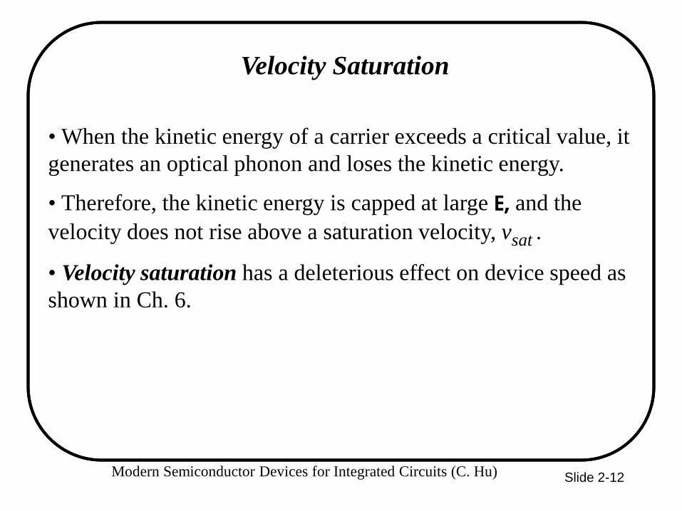
Velocity Saturation
• When the kinetic energy of a carrier exceeds a critical value, it generates an optical phonon and loses the kinetic energy.
• Therefore, the kinetic energy is capped at large E, and the velocity does not rise above a saturation velocity, vsat .
• Velocity saturation has a deleterious effect on device speed as shown in Ch. 6.

Modern Semiconductor Devices for Integrated Circuits (C. Hu) Slide 2-13
2.2.3 Drift Current and Conductivity
J p
ν
E
unit area
+
+
Jp = qpv A/cm2 or C/cm2·sec
If p = 1015cm-3 and v = 104 cm/s, then Jp= 1.6×10-19C × 1015cm-3 × 104cm/s = 22 A/cm 1.6cmC/s 6.1 =⋅
EXAMPLE:
Hole current density

Modern Semiconductor Devices for Integrated Circuits (C. Hu) Slide 2-14
Jp,drift = qpv = qpµpE
Jn,drift = –qnv = qnµnE
Jdrift = Jn,drift + Jp,drift = σ E =(qnµn+qpµp)E
conductivity (1/ohm-cm) of a semiconductor is σ = qnµn + qpµp
∴
2.2.3 Drift Current and Conductivity
1/σ = is resistivity (ohm-cm)

Modern Semiconductor Devices for Integrated Circuits (C. Hu) Slide 2-15
N-type
P-type
Relationship between Resistivity and Dopant Density
ρ = 1/σ
DOPA
NT D
ENSI
TY cm
-3
RESISTIVITY (Ω⋅cm)

Modern Semiconductor Devices for Integrated Circuits (C. Hu) Slide 2-16
EXAMPLE: Temperature Dependence of Resistance
(a) What is the resistivity (ρ) of silicon doped with 1017cm-3 of arsenic?
Solution: (a) Using the N-type curve in the previous figure, we find that ρ = 0.084 Ω-cm.
(b) What is the resistance (R) of a piece of this silicon material 1µm long and 0.1 µm2 in cross-sectional area?
(b) R = ρL/A = 0.084 Ω-cm × 1 µm / 0.1 µm2
= 0.084 Ω-cm × 10-4 cm/ 10-10 cm2 = 8.4 × 10⁻⁴ Ω

Modern Semiconductor Devices for Integrated Circuits (C. Hu) Slide 2-17
EXAMPLE: Temperature Dependence of Resistance
By what factor will R increase or decrease from T=300 K to T=400 K? Solution: The temperature dependent factor in σ (and therefore ρ) is µn. From the mobility vs. temperature curve for 1017cm-3, we find that µn decreases from 770 at 300K to 400 at 400K. As a result, R increases by
93.1400770
=

Modern Semiconductor Devices for Integrated Circuits (C. Hu) Slide 2-18
2.3 Diffusion Current
Particles diffuse from a higher-concentration location to a lower-concentration location.

Modern Semiconductor Devices for Integrated Circuits (C. Hu) Slide 2-19
2.3 Diffusion Current
dxdnqDJ ndiffusionn =, dx
dpqDJ pdiffusionp −=,
D is called the diffusion constant. Signs explained: n p
x x

Modern Semiconductor Devices for Integrated Circuits (C. Hu) Slide 2-20
Total Current – Review of Four Current Components
Jn = Jn,drift + Jn,diffusion = qnµnE + dx
dnqDn
Jp = Jp,drift + Jp,diffusion = qpµpE – dx
dpqDp
JTOTAL = Jn + Jp

Modern Semiconductor Devices for Integrated Circuits (C. Hu) Slide 2-21
2.4 Relation Between the Energy Diagram and V, E
E(x)= dxdE
q1
dxdE
q1
dxdV vc ==−
Ec and Ev vary in the opposite direction from the voltage. That is, Ec and Ev are higher where the voltage is lower.
V(x)
0.7V
x0
x
E f (x)
E
0.7V
-
+
E c (x)
E v (x)
N- + –
0.7eV
N type Si
Modern Semiconductor Devices for Integrated Circuits (C. Hu) Slide 2-22
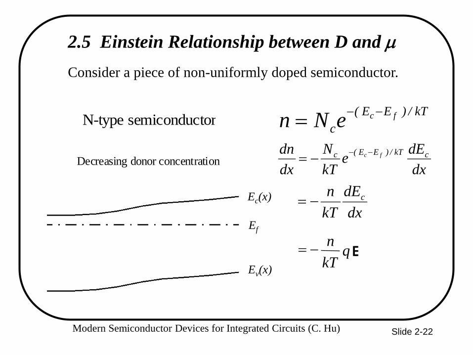
2.5 Einstein Relationship between D and µ
dxdEe
kTN
dxdn ckT/)EE(c fc −−−=
dxdE
kTn c−=
kT/)EE(
cfceNn −−=
Consider a piece of non-uniformly doped semiconductor.
Ev(x)
Ec(x)
Ef
n-type semiconductor
Decreasing donor concentration
N-type semiconductor
E q kT n − =

Modern Semiconductor Devices for Integrated Circuits (C. Hu) Slide 2-23
2.5 Einstein Relationship between D and µ
E q kT n
dx dn − =
0 = + = dx dn qD qn J n n n E µ at equilibrium.
E E kT qD qn qn n
n − = µ 0
nn qkTD µ=
These are known as the Einstein relationship.
p p q kT D µ = Similarly,

Modern Semiconductor Devices for Integrated Circuits (C. Hu) Slide 2-24
EXAMPLE: Diffusion Constant
What is the hole diffusion constant in a piece of silicon with µp = 410 cm2 V-1s-1 ? Solution:
Remember: kT/q = 26 mV at room temperature.
/scm 11sVcm 410)mV 26( 2112 =⋅=
= −−
pp qkTD µ

Modern Semiconductor Devices for Integrated Circuits (C. Hu) Slide 2-25
2.6 Electron-Hole Recombination
•The equilibrium carrier concentrations are denoted with n0 and p0. •The total electron and hole concentrations can be different from n0 and p0 . •The differences are called the excess carrier concentrations n’ and p’.
'0 nnn +≡'0 ppp +≡

Modern Semiconductor Devices for Integrated Circuits (C. Hu) Slide 2-26
Charge Neutrality
•Charge neutrality is satisfied at equilibrium (n’= p’= 0). • When a non-zero n’ is present, an equal p’ may be assumed to be present to maintain charge equality and vice-versa. •If charge neutrality is not satisfied, the net charge will attract or repel the (majority) carriers through the drift current until neutrality is restored.
'p'n =

Modern Semiconductor Devices for Integrated Circuits (C. Hu) Slide 2-27
Recombination Lifetime
•Assume light generates n’ and p’. If the light is suddenly turned off, n’ and p’ decay with time until they become zero. •The process of decay is called recombination. •The time constant of decay is the recombination time or carrier lifetime, τ . •Recombination is nature’s way of restoring equilibrium (n’= p’= 0).

Modern Semiconductor Devices for Integrated Circuits (C. Hu) Slide 2-28
•τ ranges from 1ns to 1ms in Si and depends on the density of metal impurities (contaminants) such as Au and Pt. •These deep traps capture electrons and holes to facilitate recombination and are called recombination centers.
Recombination Lifetime
Ec
Ev
Direct Recombination is unfavorable in silicon
Recombination centers

Direct and Indirect Band Gap
Direct band gap Example: GaAs Direct recombination is efficient as k conservation is satisfied.
Indirect band gap Example: Si
Direct recombination is rare as k conservation is not satisfied
Trap
Modern Semiconductor Devices for Integrated Circuits (C. Hu)

Modern Semiconductor Devices for Integrated Circuits (C. Hu) Slide 2-30
τn
dtnd ′
−=′
dtpdpn
dtnd ′
=′
−=′
−=′
ττ
Rate of recombination (s-1cm-3)
pn ′=′

Modern Semiconductor Devices for Integrated Circuits (C. Hu)
Slide 2-31
EXAMPLE: Photoconductors
A bar of Si is doped with boron at 1015cm-3. It is exposed to light such that electron-hole pairs are generated throughout the volume of the bar at the rate of 1020/s·cm3. The recombination lifetime is 10µs. What are (a) p0 , (b) n0 , (c) p’, (d) n’, (e) p , (f) n, and (g) the np product?

Modern Semiconductor Devices for Integrated Circuits (C. Hu)
Slide 2-32
EXAMPLE: Photoconductors Solution: (a) What is p0? p0 = Na = 1015 cm-3
(b) What is n0 ? n0 = ni
2/p0 = 105 cm-3
(c) What is p’? In steady-state, the rate of generation is equal to the
rate of recombination. 1020/s-cm3 = p’/τ ∴ p’= 1020/s-cm3 · 10-5s = 1015 cm-3

Modern Semiconductor Devices for Integrated Circuits (C. Hu) Slide 2-33
EXAMPLE: Photoconductors (d) What is n’? n’= p’= 1015 cm-3 (e) What is p? p = p0 + p’= 1015cm-3 + 1015cm-3 = 2×1015cm-3
(f) What is n? n = n0 + n’= 105cm-3 + 1015cm-3 ~ 1015cm-3 since n0 << n’
(g) What is np? np ~ 2×1015cm-3 ·1015cm-3 = 2×1030 cm-6 >> ni
2 = 1020 cm-6. The np product can be very different from ni
2.

Modern Semiconductor Devices for Integrated Circuits (C. Hu) Slide 2-34
2.7 Thermal Generation
If n’ is negative, there are fewer electrons than the equilibrium value. As a result, there is a net rate of thermal generation at the rate of |n′|/τ .

Modern Semiconductor Devices for Integrated Circuits (C. Hu) Slide 2-35
2.8 Quasi-equilibrium and Quasi-Fermi Levels • Whenever n’ = p’ ≠ 0, np ≠ ni
2. We would like to preserve and use the simple relations:
• But these equations lead to np = ni2. The solution is to introduce
two quasi-Fermi levels Efn and Efp such that
kTEEc
fceNn /)( −−=
kTEEv
vfeNp /)( −−=
kTEEc
fnceNn /)( −−=
kTEEv
vfpeNp /)( −−=Even when electrons and holes are not at equilibrium, within each group the carriers can be at equilibrium. Electrons are closely linked to other electrons but only loosely to holes.

Modern Semiconductor Devices for Integrated Circuits (C. Hu) Slide 2-36
EXAMPLE: Quasi-Fermi Levels and Low-Level Injection
Consider a Si sample with Nd=1017cm-3 and n’=p’=1015cm-3. (a) Find Ef . n = Nd = 1017 cm-3 = Ncexp[–(Ec– Ef)/kT] ∴ Ec– Ef = 0.15 eV. (Ef is below Ec by 0.15 eV.)
Note: n’ and p’ are much less than the majority carrier concentration. This condition is called low-level injection.
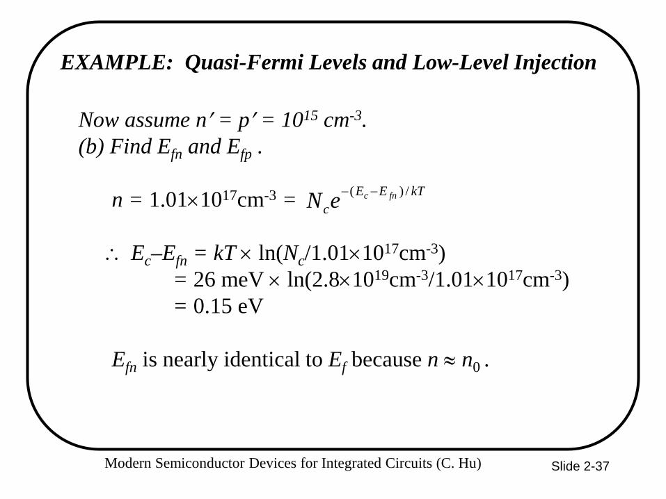
Modern Semiconductor Devices for Integrated Circuits (C. Hu) Slide 2-37
Now assume n′ = p′ = 1015 cm-3. (b) Find Efn and Efp . n = 1.01×1017cm-3 = ∴ Ec–Efn = kT × ln(Nc/1.01×1017cm-3) = 26 meV × ln(2.8×1019cm-3/1.01×1017cm-3) = 0.15 eV Efn is nearly identical to Ef because n ≈ n0 .
kTEEc
fnceN /)( −−
EXAMPLE: Quasi-Fermi Levels and Low-Level Injection

Modern Semiconductor Devices for Integrated Circuits (C. Hu) Slide 2-38
EXAMPLE: Quasi-Fermi Levels
p = 1015 cm-3 =
∴ Efp–Ev = kT × ln(Nv/1015cm-3) = 26 meV × ln(1.04×1019cm-3/1015cm-3) = 0.24 eV
kTEEv
vfpeN /)( −−
Ec
Ev
Efp
Ef Efn

Modern Semiconductor Devices for Integrated Circuits (C. Hu) Slide 2-39
2.9 Chapter Summary
dxdnqDJ ndiffusionn =,
dxdpqDJ pdiffusionp −=,
nn qkTD µ=
pp qkTD µ=
E p p v µ =
E n n v µ =
E p drift p qp J µ = ,
E n drift n qn J µ = ,
-

Modern Semiconductor Devices for Integrated Circuits (C. Hu)
Slide 2-40
2.9 Chapter Summary τ is the recombination lifetime. n’ and p’ are the excess carrier concentrations.
n = n0+ n’ p = p0+ p’
Charge neutrality requires n’= p’. rate of recombination = n’/τ = p’/τ Efn and Efp are the quasi-Fermi levels of electrons and holes.
kTEEv
vfpeNp /)( −−=
kTEEc
fnceNn /)( −−=

Modern Semiconductor Devices for Integrated Circuits (C. Hu) Slide 3-1
Chapter 3 Device Fabrication Technology
About 1020 transistors (or 10 billion for every person in the world) are manufactured every year.
VLSI (Very Large Scale Integration) ULSI (Ultra Large Scale Integration) GSI (Giga-Scale Integration)
Variations of this versatile technology are used for flat-panel displays, micro-electro-mechanical systems (MEMS), and chips for DNA screening...

Slide 3-2
3.1 Introduction to Device Fabrication
Oxidation
Lithography & Etching
Ion Implantation
Annealing & Diffusion
Modern Semiconductor Devices for Integrated Circuits (C. Hu)

Slide 3-3
Si Wafers
O N2
H2O or TCE(trichloroethylene)
Quartz tube
Resistance-heated furnace
Flowcontroller
3.2 Oxidation of Silicon
Modern Semiconductor Devices for Integrated Circuits (C. Hu)

Slide 3-4
3.2 Oxidation of Silicon Si + O2 → SiO2
Si +2H2O → SiO2 + 2H2
Dry Oxidation : Wet Oxidation :
Modern Semiconductor Devices for Integrated Circuits (C. Hu)

Slide 3-5
EXAMPLE : Two-step Oxidation (a) How long does it take to grow 0.1µm of dry oxide at 1000 oC ?
(b) After step (a), how long will it take to grow an additional 0.2µm of oxide at 900 oC in a wet ambient ?
Solution:
(a) From the “1000oC dry” curve in Slide 3-3, it takes 2.5 hr to grow 0.1µm of oxide.
(b) Use the “900oC wet” curve only. It would have taken 0.7hr to grow the 0.1 µm oxide and 2.4hr to grow 0.3 µm oxide from bare silicon. The answer is 2.4hr–0.7hr = 1.7hr.
3.2 Oxidation of Silicon
Modern Semiconductor Devices for Integrated Circuits (C. Hu)

Slide 3-6
3.3 Lithography
Resist Coating (a) Development (c)
Etching and Resist Strip (d)
Photoresist
Oxide Si
Exposure (b)
Si
Si
Positive resist
Negative resist
Si
Si
Optical Lens system
Deep Ultraviolet Light
Photomask with opaque and clear patterns
Modern Semiconductor Devices for Integrated Circuits (C. Hu)

Slide 3-7
3.3 Lithography Photolithography Resolution Limit, R
• R ≥ kλ due to optical diffraction • Wavelength λ needs to be minimized. (248 nm, 193 nm, 157 nm?) • k (<1) can be reduced will • Large aperture, high quality lens
• Small exposure field, step-and-repeat using “stepper” • Optical proximity correction • Phase-shift mask, etc.
• Lithography is difficult and expensive. There can be 40 lithography steps in an IC process.
Modern Semiconductor Devices for Integrated Circuits (C. Hu)

Slide 3-8
3.3 Lithography
Wafers are being loaded into a stepper in a clean room.
Modern Semiconductor Devices for Integrated Circuits (C. Hu)

Slide 3-9
Photo Mask
PhotoresistWafer
Water
(a) (b)
Photo MaskPhoto Mask
PhotoresistWafer
PhotoresistWafer
Water
(a) (b)
conventional dry lithography wet or immersion lithography
3.3.1 Wet Lithography
Modern Semiconductor Devices for Integrated Circuits (C. Hu)

Slide 3-10
Reflective “photomask”
Laser produced plasma emitting EUV
Extreme UV Lithography (13nm wavelength)
No suitable lens material at this wavelength. Optics is based on mirrors with nm flatness.
Modern Semiconductor Devices for Integrated Circuits (C. Hu)

Slide 3-11
• Electron Beam Writing : Electron beam(s) scans and exposed electron resist on wafer. Ready technology with relatively low throughput.
• Electron Projection Lithography : Exposes a complex pattern using mask and electron lens similar to optical lithography. • Nano-imprint : Patterns are etched into a durable material to
make a “stamp.” This stamp is pressed into a liquid film over the wafer surface. Liquid is hardened with UV to create an imprint of the fine patterns.
Beyond Optical Lithography
Modern Semiconductor Devices for Integrated Circuits (C. Hu)

Slide 3-12
3.4 Pattern Transfer–Etching Isotropic etching Anisotropic etching
SiO2
SiO2
SiO2
(1)
(2)
photoresist
photoresist
SiO2
(1)
(2)
photoresist
photoresist
SiO2
SiO2
Modern Semiconductor Devices for Integrated Circuits (C. Hu)

Slide 3-13
3.4 Pattern Transfer–Etching
Cross-section View Top View
Reactive-Ion Etching Systems
Gas Inlet
RF Vacuum
Wafers Gas Baffle
RF
Modern Semiconductor Devices for Integrated Circuits (C. Hu)

Slide 3-14
3.4 Pattern Transfer–Etching
Dry Etching (also known as Plasma Etching, or Reactive-Ion Etching) is anisotropic. • Silicon and its compounds can be etched by plasmas containing F. • Aluminum can be etched by Cl. • Some concerns : - Selectivity and End-Point Detection - Plasma Process-Induced Damage or Wafer Charging Damage and Antenna Effect
Modern Semiconductor Devices for Integrated Circuits (C. Hu)

Slide 3-15
Scanning electron microscope view of a plasma-etched 0.16 µm pattern in polycrystalline silicon film.
Modern Semiconductor Devices for Integrated Circuits (C. Hu)

Slide 3-16
3.5 Doping 3.5.1 Ion Implantation
• The dominant doping method • Excellent control of dose (cm-2) • Good control of implant depth with energy (KeV to MeV) • Repairing crystal damage and dopant activation requires
annealing, which can cause dopant diffusion and loss of depth control.
Dopant ions
Modern Semiconductor Devices for Integrated Circuits (C. Hu)
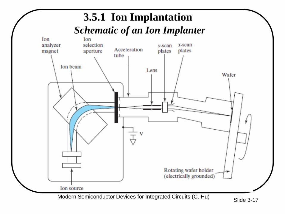
Slide 3-17
3.5.1 Ion Implantation Schematic of an Ion Implanter
Modern Semiconductor Devices for Integrated Circuits (C. Hu)

Slide 3-18
3.5.1 Ion implantation
Phosphorous density profile after implantation
Modern Semiconductor Devices for Integrated Circuits (C. Hu)

Slide 3-19
3.5.1 Ion Implantation Model of Implantation Doping Profile (Gaussian)
22 2/)(
)(2)( RRxi e
RNxN ∆−−⋅
∆⋅=
π
Ni : dose (cm-2) R : range or depth ∆R : spread or sigma
Modern Semiconductor Devices for Integrated Circuits (C. Hu)

Slide 3-20
Other Doping Methods
• Gas-Source Doping : For example, dope Si with P using POCl3.
• Solid-Source Doping : Dopant diffuses from a doped solid film (SiGe or oxide) into Si. • In-Situ Doping : Dopant is introduced while a Si
film is being deposited.
Modern Semiconductor Devices for Integrated Circuits (C. Hu)

Slide 3-21
3.6 Dopant Diffusion
Dtxo eDt
NtxN 4/2
),( −
⋅=
πN : Nd or Na (cm-3) No : dopant atoms per cm2
t : diffusion time D : diffusivity, is the approximate distance of dopant diffusion
Dt
p-type Si
SiO 2
n-type diffusion layer
Junction depth
Modern Semiconductor Devices for Integrated Circuits (C. Hu)

Slide 3-22
3.6 Dopant Diffusion
• Some applications need very deep junctions (high T, long t). Others need very shallow junctions (low T, short t).
• D increases with increasing temperature.
Modern Semiconductor Devices for Integrated Circuits (C. Hu)

Slide 3-23
3.6 Dopant Diffusion Shallow Junction and Rapid Thermal Annealing
• After ion implantation, thermal annealing is required. Furnace annealing takes minutes and causes too much diffusion of dopants for some applications. • In rapid thermal annealing (RTA), the wafer is heated to high temperature in seconds by a bank of heat lamps.
•In flash annealing (100mS) and laser annealing (<1uS), dopant ddiffusion is practically eliminated.
Modern Semiconductor Devices for Integrated Circuits (C. Hu)

Slide 3-24
3.7 Thin-Film Deposition Three Kinds of Solid
Crystalline Polycrystalline
Example: Silicon wafer Thin film of Si or metal. Thin film of
SiO2 or Si3N4.
Amorphous
Modern Semiconductor Devices for Integrated Circuits (C. Hu)

Slide 3-25
3.7 Thin-Film Deposition
• Advanced MOSFET gate dielectric
• Poly-Si film for transistor gates
• Metal layers for interconnects • Dielectric between metal layers • Encapsulation of IC
Examples of thin films in integrated circuits
Modern Semiconductor Devices for Integrated Circuits (C. Hu)

Slide 3-26
3.7.1 Sputtering
YYYYYYYY
YYYYYYYY
YYYYYY YY
YYYYYYYYYYYY
Y YYYYYYYYYY
YYYYY
YYYY YYYYYYYYYYYYYYYYYY
YYYYYYYYYYYY YYYYYYYYY YYYYYYY
YYYYYY YYYYYYYYYYY Y YYYYYYY
YYYYYYY YYYYYYYY YYYYYY
YY YYY YYY
Y YY
Y YY YYYYYYYYYYYYY YYYY
Target materialdeposited on wafer
Si Wafer
Ion (Ar+)YY Y
Sputtering target
Atoms sputtered out of the target
Schematic Illustration of Sputtering Process
Modern Semiconductor Devices for Integrated Circuits (C. Hu)

Slide 3-27
3.7.2 Chemical Vapor Deposition (CVD)
Thin film is formed from gas phase components. Modern Semiconductor Devices for Integrated Circuits (C. Hu)

Slide 3-28
Some Chemical Reactions of CVD
Poly-Si : SiH4 (g) Si (s) + 2H2 (g) Si3N4 : 3SiH2Cl2 (g)+4NH3 (g) Si3N4 (s)+6HCl(g)+6H2 (g) SiO2 : SiH4 (g) + O2 (g) SiO2 (s) + 2H2 (g) or SiH2Cl2 (g)+2N2O (g) SiO2 (s)+2HCl (g)+2N2 (g)
Modern Semiconductor Devices for Integrated Circuits (C. Hu)

Slide 3-29
Two types of CVD equipment: • LPCVD (Low Pressure CVD) : Good uniformity. Used for poly-Si, oxide, nitride. • PECVD (Plasma Enhanced CVD) : Low temperature process and high deposition rate. Used for oxide, nitride, etc.
3.7.2 Chemical Vapor Deposition (CVD)
Modern Semiconductor Devices for Integrated Circuits (C. Hu)

Slide 3-30
Si Wafers
Quartz tube
Resistance-heated furnacePressure sensor
Gas control Source gases
Pump
Trap exhaust To
system
LPCVD Systems
3.7.2 Chemical Vapor Deposition (CVD)
Modern Semiconductor Devices for Integrated Circuits (C. Hu)

Slide 3-31
3.7.2 Chemical Vapor Deposition (CVD)
PECVD Systems
Cold Wall Parallel Plate
Hot Wall Parallel Plate Pump
Plasma Electrodes
Power leads
Wafers
Gas Inlet
Wafers Gas Injection Ring Pump
Heater Coil
Modern Semiconductor Devices for Integrated Circuits (C. Hu)

SiO2
SiO2
Substrate
SiO2
SiO2
Substrate
Epi film
(b)
Substrate
Substrate
Epi film
(a)
Si Si
Si Si
Slide 3-32
3.7.3 Epitaxy (Deposition of Single-Crystalline Film) Epitaxy Selective Epitaxy
Modern Semiconductor Devices for Integrated Circuits (C. Hu)

Slide 3-33
3.8 Interconnect – The Back-end Process
Dopant diffusion regionSi
SiO2
Al-Cu
(a)
Sidiffusion regionCoSi
2
M etal 1
Me tal 2
M etal 3
Dielectric
Dielectric
Encapsulation
(b)
Dielectric
via or plug
silicide
Al or Cu
Modern Semiconductor Devices for Integrated Circuits (C. Hu)

Slide 3-34
SEM: Multi-Level Interconnect (after removing the dielectric) 3.8 Interconnect – The Back-end Process
Modern Semiconductor Devices for Integrated Circuits (C. Hu)

Slide 3-35
Copper Interconnect • Al interconnect is prone to voids formation by
electromigration.
• Cu has excellent electromigration reliability and 40% lower resistance than Al.
• Because dry etching of copper is difficult (copper etching products tend to be non-volatile), copper patterns are defined by a damascene process.
3.8 Interconnect – The Back-end Process
Modern Semiconductor Devices for Integrated Circuits (C. Hu)

Slide 3-36
dielectric
dielectric dielectric
dielectric
Cu
Cu
liner liner
(a) (b)
(c) (d)
Copper Damascene Process
•Chemical-Mechanical Polishing (CMP) removes unwanted materials.
•Barrier liner prevents Cu diffusion.
3.8 Interconnect – The Back-end Process
Modern Semiconductor Devices for Integrated Circuits (C. Hu)

Slide 3-37
3.8 Interconnect – The Back-end Process
Planarization
• A flat surface is highly desirable for subsequent lithography and etching. • CMP (Chemical-Mechanical Polishing) is used to planarize each layer of dielectric in the interconnect system. Also used in the front-end process.
Modern Semiconductor Devices for Integrated Circuits (C. Hu)

Slide 3-38
3.9 Testing, Assembly, and Qualification
• Wafer acceptance test • Die sorting • Wafer sawing or laser cutting • Packaging • Flip-chip solder bump technology • Multi-chip modules • Burn-in • Final test • Qualification
Modern Semiconductor Devices for Integrated Circuits (C. Hu)

Slide 3-39
3.10 Chapter Summary–A Device Fabrication Example
Wafer
Oxidation
Lithography
Etching
Annealing & Diffusion
Al Sputtering
(0)
Positive resist SiO2
P-Si
P-Si
SiO2
P-Si
Mask
UV
SiO2 SiO2
P-Si
(1)
(2)
(3)
SiO2
UV
Lithography
SiO2 SiO2
SiO 2 SiO2
PN+
SiO2 SiO2
PN+
P-Si
SiO2 SiO2
PN+
Mask
Al Res is t
(4)
Arsenic implantation
Al
UV
(7)
(5)
(6)
Al
UV
Ion Implantation
Modern Semiconductor Devices for Integrated Circuits (C. Hu)

Slide 3-40
Metal etching
CVD nitride deposition
Lithography and etching
Back Side milling
Back side metallization
Dicing, wire bonding, and packaging
3.10 Chapter Summary–A Device Fabrication Example
S iO2 S iO2
PN+
(8)
(9)
SiO2 SiO2
PN+
SiO2 SiO2
PN+
(10)
SiO2
SiO2
PN+
(11)
Al
Si3 N4
Si3 N4
Si3 N4
Al
Al
Al
Photoresist
SiO2 SiO 2
PN+
(12)
SiO2 SiO2
PN+
(13)
Si3 N4
Si3N4
Al
Al
Au
Au
wire
Plastic package
metal leads
Modern Semiconductor Devices for Integrated Circuits (C. Hu)

Modern Semiconductor Devices for Integrated Circuits (C. Hu) Slide 4-1
Chapter 4 PN and Metal-Semiconductor Junctions
PN junction is present in perhaps every semiconductor device.
diode symbol
N P
V I
– +
4.1 Building Blocks of the PN Junction Theory
V
I
Reverse bias Forward bias
Donor ions
N-type
P-type

Modern Semiconductor Devices for Integrated Circuits (C. Hu) Slide 4-2
4.1.1 Energy Band Diagram of a PN Junction
A depletion layer exists at the PN junction where n ≈ 0 and p ≈ 0.
Ef is constant at equilibrium
Ec and Ev are smooth, the exact shape to be determined.
Ec and Ev are known relative to Ef
N-region P-region (a) Ef
(c)
Ec
Ev Ef
(b)
Ec
Ef Ev
Ev
Ec
(d)
Depletion layer
Neutral P-region
Neutral N-region
Ec
Ev Ef

Modern Semiconductor Devices for Integrated Circuits (C. Hu) Slide 4-3
4.1.2 Built-in Potential
Can the built-in potential be measured with a voltmeter?
(b)
(c)
(a) N-type N d
P-type N a Nd Na
Ef
Ec
Ev
q
φbi
xN xP x 0
V
φbi

Modern Semiconductor Devices for Integrated Circuits (C. Hu) Slide 4-4
4.1.2 Built-in Potential
−=−=
d
c
i
acbi N
Nn
NNq
kTAB lnln 2φ
d
ckTAqcd N
Nq
kTAeNNn ln=⇒== − N-region
2lni
adbi n
NNq
kT=φ
2
2
lni
ackTBqc
a
i
nNN
qkTBeN
Nnn =⇒== −P-region

Modern Semiconductor Devices for Integrated Circuits (C. Hu) Slide 4-5
4.1.3 Poisson’s Equation Gauss’s Law:
εs: permittivity (~12εo for Si) ρ: charge density (C/cm3)
Poisson’s equation
∆ x
ρ E ( x ) E ( x + ∆ x )
x

Modern Semiconductor Devices for Integrated Circuits (C. Hu) Slide 4-6
4.2.1 Field and Potential in the Depletion Layer
On the P-side of the depletion layer, ρ = –qNa
On the N-side, ρ = qNd
4.2 Depletion-Layer Model
s
a qN dx d
ε − = E
) ( ) ( 1 x x qN C x qN x P s
a
s
a − = + − = ε ε E
) ( ) ( N s
d x x qN x - = ε E
N P
D eple tion La yer N e utral R egi on
xn 0 xp
x xp
xn
qNd
–qNa
x
E
xn xp
ρ
0
N eut ra l Re gion
N
N
N P
P
P

Modern Semiconductor Devices for Integrated Circuits (C. Hu) Slide 4-7
4.2.1 Field and Potential in the Depletion Layer
The electric field is continuous at x = 0.
Na |xP| = Nd|xP|
Which side of the junction is depleted more?
A one-sided junction is called a N+P junction or P+N junction
N P
D eple tion La yer N e utral R egi on
–xn 0 xp
N eut ra l Re gion
N P

Modern Semiconductor Devices for Integrated Circuits (C. Hu)
Slide 4-8
4.2.1 Field and Potential in the Depletion Layer On the P-side,
Arbitrarily choose the voltage at x = xP as V = 0.
On the N-side,
2)(2
)( xxqNxV Ps
a −=ε
2)(2
)( Ns
d xxqNDxV −−=ε
2)(2 N
s
dbi xxqN
−−=ε
φ
x
E
xn xp
Ec
Ef Ev
φbi , built-in potential
0
xn xpx
φbi
V
N
N
P
P

Modern Semiconductor Devices for Integrated Circuits (C. Hu)
Slide 4-9
4.2.2 Depletion-Layer Width
V is continuous at x = 0
If Na >> Nd , as in a P+N junction,
What about a N+P junction?
where density dopant lighterNNN ad
1111≈+=
+==−
da
bisdepNP NNq
Wxx 112 φε
Nd
bisdep x
qNW ≈=
φε2
qNW bisdep φε2=
N P
D eple tion La yer N e utral R egi on
–xn 0 xp
N eut ra l Re gion
0 ≅ = a d N P N N x x | | | |
P N

Modern Semiconductor Devices for Integrated Circuits (C. Hu) Slide 4-10
EXAMPLE: A P+N junction has Na=1020 cm-3 and Nd =1017cm-3. What is a) its built in potential, b)Wdep , c)xN , and d) xP ?
Solution: a) b) c) d)
V 1cm10
cm1010lnV026.0ln 620
61720
2 ≈×
== −
−
i
adbi n
NNq
kTφ
μm 12.010106.1
11085.812222/1
1719
14
=
××
××××=≈ −
−
d
bisdep qN
W φε
μm 12.0=≈ depN Wx
0Å 2.1μm102.1 4 ≈=×== −adNP NNxx

Modern Semiconductor Devices for Integrated Circuits (C. Hu) Slide 4-11
4.3 Reverse-Biased PN Junction
densitydopantlighterNNN ad 1111
≈+=
• Does the depletion layer widen or shrink with increasing reverse bias?
+ – V
N P
qNbarrier potential
qNVW srbis
dep⋅
=+
=εφε 2|)|(2
(b) reverse-biased
qV
Ec
Ec Efn
Ev
qφbi + qV Efp Ev
(a) V = 0
Ec
Ef Ev
Ef
Ev
qφbi Ec

Modern Semiconductor Devices for Integrated Circuits (C. Hu) Slide 4-12
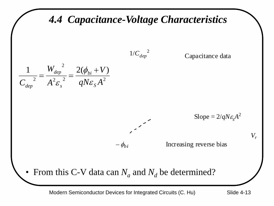
4.4 Capacitance-Voltage Characteristics
• Is Cdep a good thing? • How to minimize junction capacitance?
dep
sdep W
AC ε=
N P
Nd Na
Conductor Insulator Conductor
Wde p
Reverse biased PN junction is a capacitor.
Modern Semiconductor Devices for Integrated Circuits (C. Hu)
Slide 4-13
4.4 Capacitance-Voltage Characteristics
• From this C-V data can Na and Nd be determined?
222
2
2)(21
AqNV
AW
C S
bi
s
dep
dep εφ
ε+
==
Vr
1/Cdep2
Increasing reverse bias
Slope = 2/qNεsA2
– φbi
Capacitance data

Modern Semiconductor Devices for Integrated Circuits (C. Hu) Slide 4-14
EXAMPLE: If the slope of the line in the previous slide is 2x10²³ F-2 V-1, the intercept is 0.84V, and A is 1 µm2, find the lighter and heavier doping concentrations Nl and Nh . Solution:
⇒= ln 2i
lhbi n
NNq
kTφ 318026.084.0
15
202
cm 108.1106
10 −×=×
== eeNnN kT
q
l
ih
biφ
• Is this an accurate way to determine Nl ? Nh ?
315
28141923
2
cm 106 )cm101085.812106.1102/(2
)/(2
−
−−−
×=
×××××××=
×= AqslopeN sl ε

Modern Semiconductor Devices for Integrated Circuits (C. Hu) Slide 4-15
4.5 Junction Breakdown
A Zener diode is designed to operate in the breakdown mode.
V
I
V B , breakdown
P N A
R
Forward Current
Small leakage Current
voltage
3.7 V
R
IC
A
B
C
D
Zener diode

Modern Semiconductor Devices for Integrated Circuits (C. Hu) Slide 4-16
4.5.1 Peak Electric Field
2 / 1
|) | ( 2 ) 0 (
+ = = r bi
s p V qN φ
ε E E
bi crit s
B qN V φ ε
− = 2
2 E
N + P N a
Neutral Region
0 x p
(a)
increasing reverse bias
x
E
x p
(b)
increasing reverse bias E p

Modern Semiconductor Devices for Integrated Circuits (C. Hu) Slide 4-17
4.5.2 Tunneling Breakdown
Dominant if both sides of a junction are very heavily doped.
V/cm 10 6 ≈ = crit p E E
V
I
Breakdown
Empty States Filled States -
Ev
Ec
pεeG J / H−=

Modern Semiconductor Devices for Integrated Circuits (C. Hu)
Slide 4-18
4.5.3 Avalanche Breakdown • impact ionization: an energetic electron generating electron and hole, which can also cause impact ionization.
qN V crit s
B 2
2 E ε
=
• Impact ionization + positive feedbackavalanche breakdown
daB N
1N1
N1V +=∝
E c E fn
E c
E v
E fp
original electron
electron-hole pair generation

Modern Semiconductor Devices for Integrated Circuits (C. Hu) Slide 4-19
4.6 Forward Bias – Carrier Injection
Minority carrier injection
– +V
N PEc
EfEv
Ec
Efp
Ev
V = 0
Ef n
Forward biased
qφbi
qV
-
+
qφbi–qV
V=0
I=0
Forward biased
Drift and diffusion cancel out

Modern Semiconductor Devices for Integrated Circuits (C. Hu) Slide 4-20
4.6 Forward Bias – Quasi-equilibrium Boundary Condition
kTEEkTEEc
kTEEc
fpfnfpcfnc eeNeNxn /)(/)(/)(P )( −−−−− ==
kTqVP
kTEEP enen fpfn /
0/)(
0 == −
• The minority carrier densities are raised by eqV/kT
• Which side gets more carrier injection?
Ec
Efp
Ev
Efn
0N 0P
x
Ec
Efn
Efp
Ev
x
Efn
xN xP

Modern Semiconductor Devices for Integrated Circuits (C. Hu) Slide 4-21
4.6 Carrier Injection Under Forward Bias– Quasi-equilibrium Boundary Condition
)1()()( 00 −=−≡′ kTqVPPPP ennxnxn
)1()()( 00 −=−≡′ kTqVNNNN eppxpxp
kT V q
a
i kT V q P e
N n e n n
2
0 ) xP ( = =
kT V q
d
i kT V q N e
N n e p p
2
0 ) ( = = xP

Modern Semiconductor Devices for Integrated Circuits (C. Hu) Slide 4-22
EXAMPLE: Carrier Injection
A PN junction has Na=1019cm-3 and Nd=1016cm-3. The applied voltage is 0.6 V. Question: What are the minority carrier concentrations at the depletion-region edges? Solution:
Question: What are the excess minority carrier concentrations? Solution:
-311026.06.00 cm 1010)( =×== eenxn kTVq
PP-314026.06.04
0 cm 1010)( =×== eepxp kTVqNN
-311110 cm 101010)()( =−=−=′ PPP nxnxn
-3144140 cm 101010)()( =−=−=′ NNN pxpxp

Modern Semiconductor Devices for Integrated Circuits (C. Hu) Slide 4-23
4.7 Current Continuity Equation
τpq
xxJxxJ pp ′
=∆
−∆+−
)()(
τpxA
qxxJ
Aq
xJA pp ′
⋅∆⋅+∆+
⋅=⋅)()(
τpq
dxdJ p ′
=−
∆x
pJp(x + ∆x)
x
area A
Jp(x)
Volume = A·∆x

Modern Semiconductor Devices for Integrated Circuits (C. Hu) Slide 4-24
4.7 Current Continuity Equation
Minority drift current is negligible; Jp= –qDpdp/dx ∴
Lp and Ln are the diffusion lengths
τpq
dxdJ p ′
=−
pp
pqdx
pdqDτ
′=2
2
22
2
ppp Lp
Dp
dxpd ′
=′
=′
τ
ppp DL τ≡
22
2
nLn
dxnd ′
=′
nnn DL τ≡

Modern Semiconductor Devices for Integrated Circuits (C. Hu) Slide 4-25
4.8 Forward Biased Junction-- Excess Carriers
22
2
pLp
dxpd ′
=′
0)( =∞′p
)1()( /0 −=′ kTqV
NN epxppp LxLx BeAexp //)( −+=′
( )N
LxxkTqVN xxeepxp pN >−=′ −− ,)1()( //
0
P N +
xP -xN 0
x

Modern Semiconductor Devices for Integrated Circuits (C. Hu) Slide 4-26
( )P
LxxkTqVP xxeenxn nP <−=′ − ,)1()( //
0
4.8 Excess Carrier Distributions
0.5
1.0
–3Ln –2Ln –Ln 0 Lp 2Lp 3Lp 4Lp
N-side
Nd = 2×1017 cm-3
pN' ∝ e–x /L
P-side
nP'∝ ex /LNa = 1017cm -3
n p
( )N
LxxkTqVN xxeepxp pN >−=′ −− ,)1()( //
0

Modern Semiconductor Devices for Integrated Circuits (C. Hu) Slide 4-27
EXAMPLE: Carrier Distribution in Forward-biased PN Diode
• Sketch n'(x) on the P-side. 313026.06.0
17
20/
2
0 cm 101010)1()1()( −==−=−=′ ee
Nnenxn kTqV
a
ikTqVPP
N-typeNd = 5×1017 cm-3
Dp =12 cm2/sτp = 1 µs
P-typeNa = 1017 cm-3
Dn=36.4 cm2/sτn = 2 µs
x
N-side P-side 10 13 cm -3
2 10 12
n’ ( = p’ )
p´ ( = n’ )

Modern Semiconductor Devices for Integrated Circuits (C. Hu)
Slide 4-28
• How does Ln compare with a typical device size?
μm 8510236 6 =××== −nnn DL τ
• What is p'(x) on the P- side?
EXAMPLE: Carrier Distribution in Forward-biased PN Diode

Modern Semiconductor Devices for Integrated Circuits (C. Hu)
Slide 4-29
4.9 PN Diode I-V Characteristics
( ) pN LxxkTVqN
p
pppN eep
LD
qdx
xpdqDJ −−−=′
−= )1()(0
( ) nP LxxkTVqP
n
nnnP een
LDq
dxxndqDJ −−=
′= )1()(
0
xJ
enLDqp
LD
qxJxJ kTVqP
n
nN
p
pPnPNpN
allat
)1()()(current Total 00
=
−
+=+=
0 P-side N-side
Jtotal
JpN JnP
x 0 P-side N-side
J total
JpN JnP
Jn = Jtotal – Jp Jp = Jtotal – Jn

Modern Semiconductor Devices for Integrated Circuits (C. Hu) Slide 4-30
The PN Junction as a Temperature Sensor
What causes the IV curves to shift to lower V at higher T ?
)1(0 −= kTVqeII
+=
an
n
dp
pi NL
DNL
DAqnI 2
0

Modern Semiconductor Devices for Integrated Circuits (C. Hu) Slide 4-31
4.9.1 Contributions from the Depletion Region
dep
depileakage τ
WqnAII += 0
Space-Charge Region (SCR) current
kTqVienpn 2/≈≈
)1(
:rate n)(generatioion recombinatNet
2/ −kTqV
dep
i enτ
)1()1( 2//0 −+−= kTqV
dep
depikTqV eτWqn
AeII
Under forward bias, SCR current is an extra current with a slope 120mV/decade
Modern Semiconductor Devices for Integrated Circuits (C. Hu) Slide 4-32
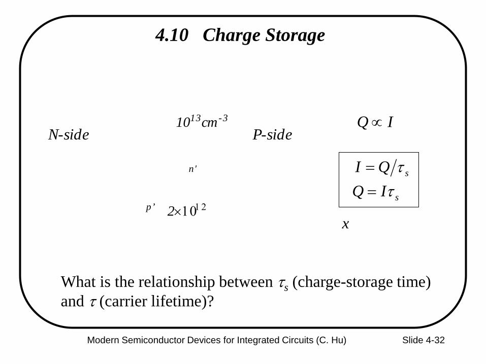
4.10 Charge Storage
What is the relationship between τs (charge-storage time) and τ (carrier lifetime)?
x
N-side P-side1013cm-3
2×10¹²
n'
p’
IQ ∝
sQI τ=
sIQ τ=

Modern Semiconductor Devices for Integrated Circuits (C. Hu)
Slide 4-33
4.11 Small-signal Model of the Diode
kTqVkTqV eIdVdeI
dVd
dVdI
RG /
0/
0 )1(1≈−==≡
What is G at 300K and IDC = 1 mA?
Diffusion Capacitance:
qkT/IG
dVdI
dVdQC DCsss τττ ====
Which is larger, diffusion or depletion capacitance?
C R V
I
q kT I e I
kT q
DC kT qV / ) ( /
0 = =

Modern Semiconductor Devices for Integrated Circuits (C. Hu) Slide 4-34
4.12 Solar Cells •Solar Cells is also known as photovoltaic cells.
•Converts sunlight to electricity with 10-30% conversion efficiency.
•1 m2 solar cell generate about 150 W peak or 25 W continuous power.
•Low cost and high efficiency are needed for wide deployment.
Part II: Application to Optoelectronic Devices

Modern Semiconductor Devices for Integrated Circuits (C. Hu) Slide 4-35
4.12.1 Solar Cell Basics
sckTVq IeII −−= )1(0
V 0.7 V
– I sc Maximum
power-output
Solar Cell IV
I
Dark IV
0
Eq.(4.9.4)
Eq.(4.12.1)
N P
-
Short Circuit
light I sc
+ (a)
E c
E v

Direct-Gap and Indirect-Gap Semiconductors
Modern Semiconductor Devices for Integrated Circuits (C. Hu) Slide 4-36
•Electrons have both particle and wave properties. •An electron has energy E and wave vector k.
indirect-gap semiconductor direct-gap semiconductor

4.12.2 Light Absorption
)(24.1
(eV)Energy Photon
m
hc
µλ
λ
=
=
x-e (x)intensity Light α∝
α(1/cm): absorption coefficient
1/α : light penetration depth
Modern Semiconductor Devices for Integrated Circuits (C. Hu)
Slide 4-37
A thinner layer of direct-gap semiconductor can absorb most of solar radiation than indirect-gap semiconductor. But Si…

4.12.3 Short-Circuit Current and Open-Circuit Voltage
Modern Semiconductor Devices for Integrated Circuits (C. Hu) Slide 4-38
∆x
pJp(x + ∆x)
x
area A
Jp(x)
Volume = A·∆x
If light shines on the N-type semiconductor and generates holes (and electrons) at the rate of G s-1cm-3 ,
pp DG
Lp
dxpd
−′
=′
22
2
If the sample is uniform (no PN junction), d2p’/dx2 = 0 p’ = GLp
2/Dp= Gτp

Solar Cell Short-Circuit Current, Isc
pLxp
p
ppp Ge
LD
qdx
xpdqDJ /)( −=′
−= τ
GDGLp p
pp τ==∞′ 2)(
Modern Semiconductor Devices for Integrated Circuits (C. Hu) Slide 4-39
)1()( / pLxp eGxp −−=′ τ
0)0( =′p
Assume very thin P+ layer and carrier generation in N region only.
GAqLAJI ppsc == )0(x
N P+
Isc
0 x
P'
Lp
Gpτ
0
G is really not uniform. Lp needs be larger than the light penetration depth to collect most of the generated carriers.

Open-Circuit Voltage
GAqLeLD
NnAqI p
kTqV
p
p
d
i −−= )1( /2
Modern Semiconductor Devices for Integrated Circuits (C. Hu) Slide 4-40
1) e (assuming /qVoc >>kT
•Total current is ISC plus the PV diode (dark) current:
•Solve for the open-circuit voltage (Voc) by setting I=0
GLeLD
Nn
pkTqV
p
p
d
i oc −= /2
0
)/ln( 2idpoc nGN
qkTV τ=
How to raise Voc ?

Modern Semiconductor Devices for Integrated Circuits (C. Hu) Slide 4-41
4.12.4 Output Power
FFVI ocsc ××= erOutput Pow
•Theoretically, the highest efficiency (~24%) can be obtained with 1.9eV >Eg>1.2eV. Larger Eg lead to too low Isc (low light absorption); smaller Eg leads to too low Voc. •Tandem solar cells gets 35% efficiency using large and small Eg materials tailored to the short and long wavelength solar light.
A particular operating point on the solar cell I-V curve maximizes the output power (I V). ×
•Si solar cell with 15-20% efficiency dominates the market now

Modern Semiconductor Devices for Integrated Circuits (C. Hu) Slide 4-42
Light emitting diodes (LEDs) • LEDs are made of compound semiconductors such as InP
and GaN.
• Light is emitted when electron and hole undergo radiative recombination.
Ec
Ev
Radiative recombination
Non-radiative recombination through traps
4.13 Light Emitting Diodes and Solid-State Lighting

Direct and Indirect Band Gap
Direct band gap Example: GaAs Direct recombination is efficient as k conservation is satisfied.
Indirect band gap Example: Si
Direct recombination is rare as k conservation is not satisfied
Trap
Modern Semiconductor Devices for Integrated Circuits (C. Hu)

Modern Semiconductor Devices for Integrated Circuits (C. Hu) Slide 4-44
4.13.1 LED Materials and Structure
)(24.1
energy photon24.1 m) ( h wavelengtLED
eVEg
≈=µ

Modern Semiconductor Devices for Integrated Circuits (C. Hu) Slide 4-45
4.13.1 LED Materials and Structure
)(eVEg
red yellow blue
Wavelength (μm) Color
Lattice constant
(Å)
InAs 0.36 3.44 6.05
InN 0.65 1.91 infrared 3.45
InP 1.36 0.92
violet
5.87
GaAs 1.42 0.87 5.66
GaP 2.26 0.55 5.46
AlP 3.39 0.51 5.45
GaN 2.45 0.37 3.19
AlN 6.20 0.20 UV 3.11
Light-emitting diode materials
compound semiconductors binary semiconductors: - Ex: GaAs, efficient emitter ternary semiconductor : - Ex: GaAs1-xPx , tunable Eg (to vary the color)
quaternary semiconductors: - Ex: AlInGaP , tunable Eg and lattice constant (for growing high quality epitaxial films on inexpensive substrates)
Eg(eV)
Red Yellow Green Blue
Modern Semiconductor Devices for Integrated Circuits (C. Hu) Slide 4-46
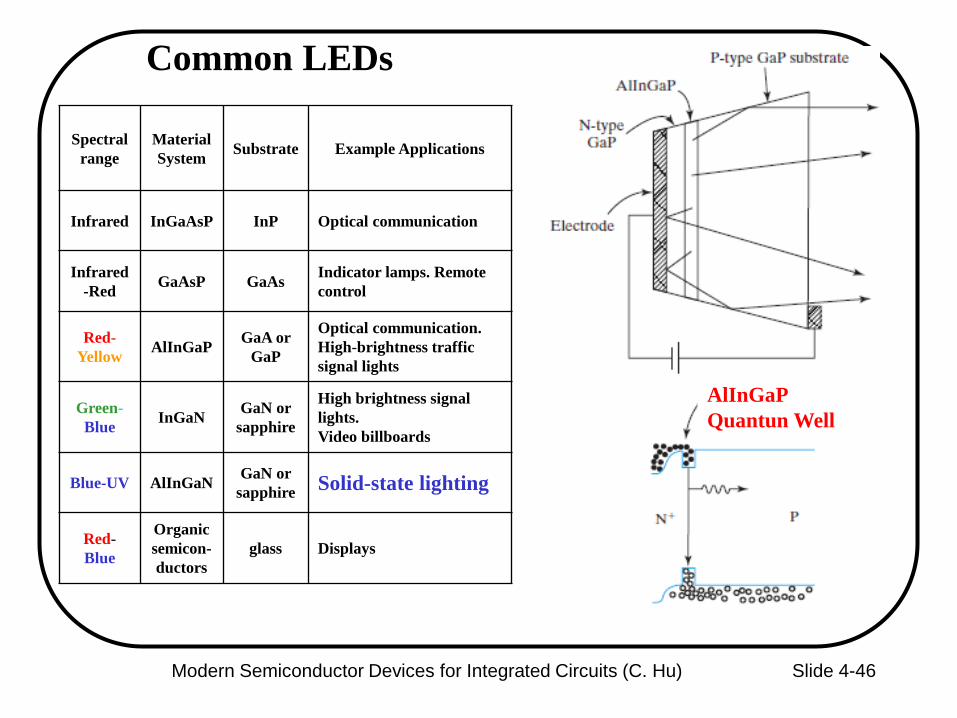
Common LEDs
Spectral range
Material System Substrate Example Applications
Infrared InGaAsP InP Optical communication
Infrared-Red GaAsP GaAs Indicator lamps. Remote
control
Red-Yellow AlInGaP GaA or
GaP
Optical communication. High-brightness traffic signal lights
Green-Blue InGaN GaN or
sapphire
High brightness signal lights. Video billboards
Blue-UV AlInGaN GaN or sapphire Solid-state lighting
Red-Blue
Organic semicon-ductors
glass Displays
AlInGaP Quantun Well

Modern Semiconductor Devices for Integrated Circuits (C. Hu)
Slide 4-47
4.13.2 Solid-State Lighting
Incandescent lamp
Compact fluorescent lamp
Tube fluorescent lamp
White LED
Theoretical limit at peak of eye sensitivity ( λ=555nm)
Theoretical limit (white light)
17 60 50-100 90-? 683 ~340
luminosity (lumen, lm): a measure of visible light energy normalized to the sensitivity of the human eye at
different wavelengths
Luminous efficacy of lamps in lumen/watt
Terms: luminosity measured in lumens. luminous efficacy,
Organic Light Emitting Diodes (OLED) : has lower efficacy than nitride or aluminide based compound semiconductor LEDs.

Modern Semiconductor Devices for Integrated Circuits (C. Hu) Slide 4-48
4.14 Diode Lasers
(d) Net Light Absorption
(e) Net Light Amplification
Stimulated emission: emitted photon has identical frequency and directionality as the stimulating photon; light wave is amplified.
(b) Spontaneous Emission
(c) Stimulated Emission
(a) Absorption
4.14.1 Light Amplification
Light amplification requires population inversion: electron occupation probability is larger for higher E states than lower E states.

Modern Semiconductor Devices for Integrated Circuits (C. Hu)
Slide 4-49
4.14.1 Light Amplification in PN Diode
gfpfn EEEqV >−=
Population inversion is achieved when
Population inversion, qV > Eg
Equilibrium, V=0

Modern Semiconductor Devices for Integrated Circuits (C. Hu) Slide 4-50
121 ≥×× GRR
•R1, R2: reflectivities of the two ends •G : light amplification factor (gain) for a round-trip travel of the light through the diode
Light intensity grows until , when the light intensity is just large enough to stimulate carrier recombinations at the same rate the carriers are injected by the diode current.
121 =×× GRR
4.14.2 Optical Feedback and Laser
light out
Cleaved crystal plane
P +
N +
Laser threshold is reached (light intensity grows by feedback) when

Modern Semiconductor Devices for Integrated Circuits (C. Hu)
Slide 4-51
4.14.2 Optical Feedback and Laser Diode • Distributed Bragg reflector (DBR) reflects light with multi-layers of semiconductors. •Vertical-cavity surface-emitting laser (VCSEL) is shown on the left. •Quantum-well laser has smaller threshold current because fewer carriers are needed to achieve population inversion in the small volume of the thin small-Eg well.

Modern Semiconductor Devices for Integrated Circuits (C. Hu) Slide 4-52
4.14.3 Laser Applications Red diode lasers: CD, DVD reader/writer
Blue diode lasers: Blu-ray DVD (higher storage density)
1.55 µm infrared diode lasers: Fiber-optic communication
Photodiodes: Reverse biased PN diode. Detects photo-generated current (similar to Isc of solar cell) for optical communication, DVD reader, etc. Avalanche photodiodes: Photodiodes operating near avalanche breakdown amplifies photocurrent by impact ionization.
4.15 Photodiodes

Modern Semiconductor Devices for Integrated Circuits (C. Hu)
Slide 4-53
Two kinds of metal-semiconductor contacts: • Rectifying Schottky diodes: metal on lightly doped silicon
•Low-resistance ohmic contacts: metal on heavily doped silicon
Part III: Metal-Semiconductor Junction
Semiconductor Devices for Integrated Circuits (C. Hu) Slide 4-54
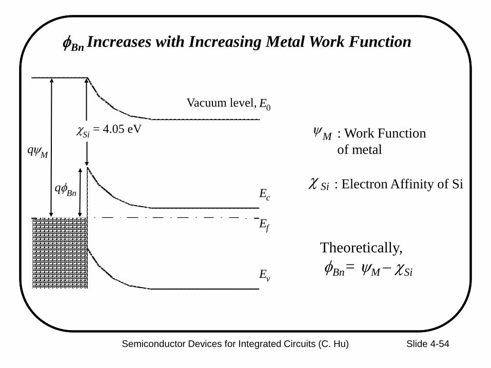
φBn Increases with Increasing Metal Work Function
Theoretically, φBn= ψM – χSi
ψ M
χ Si
: Work Function of metal
: Electron Affinity of Si
q φ Bn E c
E v
E f
E 0
q ψ M
χ Si = 4.05 eV
Vacuum level,

Modern Semiconductor Devices for Integrated Circuits (C. Hu)
Slide 4-55
4.16 Schottky Barriers Energy Band Diagram of Schottky Contact
• Schottky barrier height, φB , is a function of the metal material.
• φB is the most important parameter. The sum of qφBn and qφBp is equal to Eg .
Metal Depletion layer Neutral region
qφBn
Ec
Ec Ef
Ef
Ev
Ev qφBp
N-Si
P-Si

Modern Semiconductor Devices for Integrated Circuits (C. Hu) Slide 4-56
Schottky barrier heights for electrons and holes
φBn increases with increasing metal work function
Metal Mg Ti Cr W Mo Pd Au Ptφ Bn (V) 0.4 0.5 0.61 0.67 0.68 0.77 0.8 0.9φ Bp (V) 0.61 0.5 0.42 0.3
WorkFunction 3.7 4.3 4.5 4.6 4.6 5.1 5.1 5.7ψ m (V)
φBn + φBp ≈ Eg

Modern Semiconductor Devices for Integrated Circuits (C. Hu) Slide 4-57
• A high density of energy states in the bandgap at the metal-semiconductor interface pins Ef to a narrow range and φBn is typically 0.4 to 0.9 V
• Question: What is the typical range of φBp?
Fermi Level Pinning
q φ Bn E c
E v
E f
E 0
q ψ M
χ Si = 4.05 eV
Vacuum level,
+ −

Modern Semiconductor Devices for Integrated Circuits (C. Hu) Slide 4-58
Schottky Contacts of Metal Silicide on Si
Silicide-Si interfaces are more stable than metal-silicon interfaces. After metal is deposited on Si, an annealing step is applied to form a silicide-Si contact. The term metal-silicon contact includes and almost always means silicide-Si contacts.
Silicide: A silicon and metal compound. It is conductive similar to a metal.
Silicide ErSi1.7 HfSi MoSi2 ZrSi2 TiSi2 CoSi2 WSi2 NiSi2 Pd2Si PtSiφ
Bn (V) 0.28 0.45 0.55 0.55 0.61 0.65 0.67 0.67 0.75 0.87φ
Bp (V) 0.55 0.49 0.45 0.45 0.43 0.43 0.35 0.23φBn
φBp

Modern Semiconductor Devices for Integrated Circuits (C. Hu) Slide 4-59
Using C-V Data to Determine φB
AW
C
qNVW
NNkTq
EEqq
dep
s
d
bisdep
d
cBn
fcBnbi
ε
φε
φ
φφ
=
+=
−=
−−=
)(2
ln
)(
Question: How should we plot the CV data to extract φbi?
Ev
Ef Ec
qφbi qφBn
Ev
Ec
Ef
qφBn q(φbi + V)
qV

Modern Semiconductor Devices for Integrated Circuits (C. Hu) Slide 4-60
Once φbi is known, φΒ can be determined using
22)(21
AqNV
C sd
bi
εφ +
=
d
cBnfcBnbi N
NkTqEEqq ln)( −=−−= φφφ
Using CV Data to Determine φB
V
1 /C 2
− φ bi
Ev
Ef Ec
qφbi qφBn

Modern Semiconductor Devices for Integrated Circuits (C. Hu) Slide 4-61
4.17 Thermionic Emission Theory
2//0
//23
2
/)(2/3
2/)(
A/cm 100 where,
421
/2 /3
22
kTqo
kTqV
kTqVkTqnthxMS
nthxnth
kTVqnkTVqc
B
B
BB
eJeJ
eeTh
kqmqnvJ
mkTvmkTv
eh
kTmeNn
φ
φ
φφ
π
π
π
−
−→
−−−−
≈=
=−=
−==
==
E fn
- q( φ B − V)
q φ B qV Metal
N-type Silicon V E fm
E v
E c
x
v thx

Modern Semiconductor Devices for Integrated Circuits (C. Hu)
Slide 4-62
4.18 Schottky Diodes
V
I
Reverse bias Forward bias
V = 0
Forward biased
Reverse biased

Modern Semiconductor Devices for Integrated Circuits (C. Hu) Slide 4-63
)1(
)KA/(cm 1004
/00
/0
223
2
/20
−=−=+=
⋅≈=
=
→→
−
kTqVkTqVSMMS
n
kTq
eIIeIIIIh
kqmK
eAKTI B
π
φ
4.18 Schottky Diodes

Modern Semiconductor Devices for Integrated Circuits (C. Hu) Slide 4-64
4.19 Applications of Schottly Diodes
• I0 of a Schottky diode is 103 to 108 times larger than a PN junction diode, depending on φB . A larger I0 means a smaller forward drop V. • A Schottky diode is the preferred rectifier in low voltage, high current applications.
I
V
PN junction
Schottky
φ B
I
V
PN junction
Schottky diode
φ B diode
kTq
kTqV
BeAKTI
eII/2
0
/0 )1(
φ−=
−=

Modern Semiconductor Devices for Integrated Circuits (C. Hu) Slide 4-65
Switching Power Supply
AC DC AC AC DC
utility power
110V/220V
PN Junction rectifier
Hi-voltage
MOSFET inverter
100kHz Hi-voltage
Transformer Schottky rectifier
Lo-voltage 50A 1V
feedback to modulate the pulse width to keep V out = 1V

Modern Semiconductor Devices for Integrated Circuits (C. Hu) Slide 4-66
• There is no minority carrier injection at the Schottky junction. Therefore, Schottky diodes can operate at higher frequencies than PN junction diodes.
4.19 Applications of Schottky diodes
Question: What sets the lower limit in a Schottky diode’s forward drop? • Synchronous Rectifier: For an even lower forward drop, replace the diode with a wide-W MOSFET which is not bound by the tradeoff between diode V and leakage current.

Modern Semiconductor Devices for Integrated Circuits (C. Hu) Slide 4-67
4.20 Quantum Mechanical Tunneling
)( )(82exp 2
2
EVh
mTP H −−≈π
Tunneling probability:

Modern Semiconductor Devices for Integrated Circuits (C. Hu) Slide 4-68
4.21 Ohmic Contacts

Modern Semiconductor Devices for Integrated Circuits (C. Hu)
Slide 4-69
dBn NVHndthxdMS
ns
dBnsdep
emkTqNPvqNJ
qmh
H
qNWT
/)(2/21
/42/2/
−−→ =≈
=
=≈
φπ
επφε
4.21 Ohmic Contacts
d
Bnsdep qN
W φε2=
dBn NHeP φ−≈
Tunneling probability:
- -
x
Silicide N+ Si
Ev
Ec , Ef
φBn - -
x
V Efm
Ev
Ec , Ef
φBn – V

Modern Semiconductor Devices for Integrated Circuits (C. Hu) Slide 4-70
2//1
cmΩ2⋅∝=
≡
−→ dBn
dBnNH
dthx
NHMS
c eNHqv
edV
dJR φφ
4.21 Ohmic Contacts

Modern Semiconductor Devices for Integrated Circuits (C. Hu) Slide 4-71
4.22 Chapter Summary
The potential barrier increases by 1 V if a 1 V reverse bias is applied
junction capacitance
depletion width
2lni
adbi n
NNq
kT=φ
qNbarrier potentialW s
dep⋅
=ε2
dep
sdep W
AC ε=
Part I: PN Junction

Modern Semiconductor Devices for Integrated Circuits (C. Hu) Slide 4-72
4.22 Chapter Summary
• Under forward bias, minority carriers are injected across the jucntion.
• The quasi-equilibrium boundary condition of minority carrier densities is:
• Most of the minority carriers are injected into the more lightly doped side.
kTVqPp enxn 0)( =
kTVqNN epxp 0)( =

Modern Semiconductor Devices for Integrated Circuits (C. Hu) Slide 4-73
4.22 Chapter Summary
• Steady-state continuity equation:
• Minority carriers diffuse outward ∝ e–|x|/Lp and e–|x|/Ln
• Lp and Ln are the diffusion lengths 22
2
ppp Lp
Dp
dxpd ′
=′
=′
τ
ppp DL τ≡)1(0 −= kTVqeII
+=
an
n
dp
pi NL
DNL
DAqnI 2
0

Modern Semiconductor Devices for Integrated Circuits (C. Hu) Slide 4-74
4.22 Chapter Summary
qkT/IG DC=
Charge storage: Diffusion capacitance: Diode conductance:
GC sτ=
sIQ τ=

Modern Semiconductor Devices for Integrated Circuits (C. Hu) Slide 4-75
4.22 Chapter Summary
Part II: Optoelectronic Applications
•~100um Si or <1um direct–gap semiconductor can absorb most of solar photons with energy larger than Eg.
•Carriers generated within diffusion length from the junction can be collected and contribute to the Short Circuit Current Isc.
•Theoretically, the highest efficiency (~24%) can be obtained with 1.9eV >Eg>1.2eV. Larger Eg lead to too low Isc (low light absorption); smaller Eg leads to too low Open Circuit VoltageVoc.
FFVI ocsc ××= power cellSolar
•Si cells with ~15% efficiency dominate the market. >2x cost reduction (including package and installation) is required to achieve cost parity with base-load non-renewable electricity.

Modern Semiconductor Devices for Integrated Circuits (C. Hu) Slide 4-76
4.22 Chapter Summary
•Electron-hole recombination in direct-gap semiconductors such as GaAs produce light.
•Beyond displays, communication, and traffic lights, a new application is space lighting with luminous efficacy >5x higher than incandescent lamps. White light can be obtained with UV LED and phosphors. Cost still an issue.
LED and Solid-State Lighting
•Tenary semiconductors such as GaAsP provide tunable Eg and LED color.
•Quatenary semiconductors such as AlInGaP provide tunable Eg and lattice constants for high quality epitaxial growth on inexpensive substrates.
•Organic semiconductor is an important low-cost LED material class.

Modern Semiconductor Devices for Integrated Circuits (C. Hu) Slide 4-77
4.22 Chapter Summary
•Light is amplified under the condition of population inversion – states at higher E have higher probability of occupation than states at lower E.
•When the round-trip gain (including loss at reflector) exceeds unity, laser threshold is reached.
Laser Diodes
•Population inversion occurs when diode forward bias qV > Eg.
•Optical feedback is provided with cleaved surfaces or distributed Bragg reflectors.
•Quantum-well structures significantly reduce the threshold currents.
•Purity of laser light frequency enables long-distance fiber-optic communication. Purity of light direction allows focusing to tiny spots and enables DVD writer/reader and other application.

Modern Semiconductor Devices for Integrated Circuits (C. Hu) Slide 4-78
4.22 Chapter Summary
Part III: Metal-Semiconductor Junction
•Schottky diodes have large reverse saturation current, determined by the Schottky barrier height φB, and therefore lower forward voltage at a given current density.
kTq BeAKTI /20
φ−=
2)/4(cmΩ ⋅∝
− dnsB qNmh
c eRεφπ
•Ohmic contacts relies on tunneling. Low resistance contact requires low φB and higher doping concentration.

Modern Semiconductor Devices for Integrated Circuits (C. Hu) Slide 4-79
φBn Increases with Increasing Metal Work Function
q φ Bn E c
E v
E f
E 0
q ψ M
χ Si = 4.05 eV
Vacuum level,
Ideally, φBn= ψM – χSi

Modern Semiconductor Devices for Integrated Circuits (C. Hu) Slide 5-1
Chapter 5 MOS Capacitor
MOS: Metal-Oxide-Semiconductor
SiO2
metal
gate
Si body
Vg
gate
P-body
N+
MOS capacitor MOS transistor
Vg
SiO2 N+

Slide 5-2
This energy-band diagram for Vg = 0 is not the simplest one.
N + p o
l y s i
l i c o n
S i O
2
P - S
i l i c o
n b o
d y
Chapter 5 MOS Capacitor
Modern Semiconductor Devices for Integrated Circuits (C. Hu)
Ef , Ec Ev
Ev
Si Body
Gate
Ec
Ec
Ev Ef

Slide 5-3
5.1 Flat-band Condition and Flat-band Voltage
E0 : Vacuum level E0 – Ef : Work function E0 – Ec : Electron affinity Si/SiO2 energy barrier
sgfbV ψψ −=
χ SiO 2
=0.95 eV
9 eV
E c , E f
E v
E c
E v
E f
3.1 eV q ψ s = χ Si + ( E c – E f ) q ψ g χ Si
E 0
3.1 eV
V fb
N + -poly-Si P-body
4.8 eV
=4.05eV
E c
E v
SiO 2
The band is flat at the flat band voltage.
q
Modern Semiconductor Devices for Integrated Circuits (C. Hu)

Slide 5-4
5.2 Surface Accumulation
oxsfbg VVV ++= φ3.1eV
E c , E f
E v E 0
E c
E f E v
M O S
qV g
V ox
q φ s
Make Vg < Vfb
sφ is negligible when the surface is in accumulation.
φs : surface potential, band bending Vox: voltage across the oxide
Modern Semiconductor Devices for Integrated Circuits (C. Hu)

Slide 5-5
5.2 Surface Accumulation
fbgox VVV −=
)( fbgoxacc VVCQ −−=
oxsox CQV /−=
oxaccox CQV /−=Gauss’s Law
Modern Semiconductor Devices for Integrated Circuits (C. Hu)
Vg <Vt

Slide 5-6
ox
ssa
ox
depa
ox
dep
ox
sox C
qNC
WqNCQ
CQV
φε2==−=−=
5.3 Surface Depletion ( ) g V > V fb
E c , E f
E v
E c
E f E v
M O S
qV g
depletion region
q φ s
W dep
qV ox
- - - - SiO
2
gate
P-Si body
+ + + + + + - - - - - - -
V - - - - - - -
depletion layer charge, Q dep
- - - - - - -
Modern Semiconductor Devices for Integrated Circuits (C. Hu)

Slide 5-7
5.3 Surface Depletion
ox
ssasfboxsfbg C
qNVVVV
φεφφ
2++=++=
This equation can be solved to yield φs .
Modern Semiconductor Devices for Integrated Circuits (C. Hu)

Slide 5-8
5.4 Threshold Condition and Threshold Voltage
Threshold (of inversion): ns = Na , or (Ec–Ef)surface= (Ef – Ev)bulk , or A=B, and C = D
==
i
aBst n
Nq
kT ln22φφ
=
−
=−−=
i
a
a
v
i
vbulkvf
gB n
Nq
kTNN
qkT
nN
qkTEE
Eq lnlnln|)(
2φ
E c , E f
M O S
E v
E f
E i
E c
A
B
C = q φ Β
E v
D qV g
= qV t
φ st
Modern Semiconductor Devices for Integrated Circuits (C. Hu)

Slide 5-9
Threshold Voltage
ox
BsaBfbgt C
qNVthresholdatVV
φεφ
222 ++==
ox s fb g V φ V V + + =
At threshold,
==
i
aBst n
Nq
kT ln22φϕ
ox
Bsaox C
qNV
φε 22=
Modern Semiconductor Devices for Integrated Circuits (C. Hu)

Slide 5-10
Threshold Voltage
ox
BssubBfbt C
qNVV
φεφ
222 ±±= + for P-body,
– for N-body
Tox = 20nm
Vt(V
), N
+ −ga
te/P
-bod
y
V t(V),
P+−g
ate/
N-b
ody
Body Doping Density (cm-3)
Modern Semiconductor Devices for Integrated Circuits (C. Hu)

Slide 5-11
5.5 Strong Inversion–Beyond Threshold
E c , E f
E v
E c
E f E v
M O S
qV g
-
-
- - - -
a
Bsdmaxdep qN
WW φε 22==Vg > Vt
SiO 2
gate
P - Si substrate
++++++++++
V
V g > V t
- - - - - - - - - - - - - - -
Q dep Q inv
Modern Semiconductor Devices for Integrated Circuits (C. Hu)

Slide 5-12
Inversion Layer Charge, Qinv (C/cm2)
ox
invt
ox
inv
ox
BsaBfb
ox
inv
ox
depBfbg
CQV
CQ
CqN
VCQ
CQ
VV
−=
−++=−−+=
2222
φεφφ
)( tgoxinv VVCQ −−=∴
Modern Semiconductor Devices for Integrated Circuits (C. Hu)
Vg > Vt Vg > Vt

Slide 5-13
5.5.1 Choice of Vt and Gate Doping Type
Vt is generally set at a small positive value so that, at Vg = 0, the transistor does not have an inversion layer and current does not flow between the two N+ regions
• P-body is normally paired with N+-gate to achieve a small positive threshold voltage. • N-body is normally paired with P+-gate to achieve a small negative threshold voltage.
Modern Semiconductor Devices for Integrated Circuits (C. Hu)

Slide 5-14
Review : Basic MOS Capacitor Theory φs
2φB
Vf
b Vt
Vg accumulation depletion inversion
Wdep
W dmax
accumulation depletion inversion
∝ ( φ s ) 1/2
W dmax = (2 ε s 2 φ Β / q Ν a ) 1/2
Vg Vt
Vf
b Modern Semiconductor Devices for Integrated Circuits (C. Hu)

Slide 5-15
Review : Basic MOS Capacitor Theory
0
Vg accumulation depletion inversion
Qinv
accumulation depletion inversion
(a)
(b)
accumulation depletion inversion
(c)
Qs
0
accumulation regime
depletion regime
inversion regime
total substrate charge, Qs
invdepaccs QQQQ ++=
Qacc
Vg
Vg
Qdep=- qNaWdep
Vt Vfb
slope = − Cox
slope = − Cox Vt Vfb
Vt
Vfb
–qNaWdep
–qNaWdmax
Vg
Qinv
slope = − Cox
Vfb
Vt
Modern Semiconductor Devices for Integrated Circuits (C. Hu)

Slide 5-16
5.6 MOS CV Characteristics
g
s
g
g
dVdQ
dVdQ
C −==
C-V Meter MOS Capacitor
Modern Semiconductor Devices for Integrated Circuits (C. Hu)

Slide 5-17
5.6 MOS CV Characteristics
g
s
g
g
dVdQ
dVdQ
C −==
Qs
0
Vg
accumulation regime
depletion regime
inversion regime
Qinv
C
Vfb Vt
Cox
accumulation depletion inversion Vg
Vt
Vfb
slope = − Cox
Modern Semiconductor Devices for Integrated Circuits (C. Hu)

Slide 5-18
CV Characteristics
depox CCC111
+=
sa
fbg
ox qNVV
CC ε)(211
2
−+=
C Cox
accumulation depletion inversion Vg
Vfb Vt
In the depletion regime:
Modern Semiconductor Devices for Integrated Circuits (C. Hu)

Slide 5-19
C ox
gate
P-substrate
-
-
-
-
- - - C dmax
W dmax
- - - - - - -
AC
DC
+ + + + + + + + +
C ox
gate
P-substrate
C ox
gate
P-substrate
- - - - - - C dep Wdep
C ox
gate
P-substrate
-
Wdmax
- - - - - - - N +
DC and AC
Supply of Inversion Charge May be Limited
Accumulation Depletion
Inversion
Inversion
In each case, C = ? Modern Semiconductor Devices for Integrated Circuits (C. Hu)

Slide 5-20
Capacitor and Transistor CV (or HF and LF CV)
Modern Semiconductor Devices for Integrated Circuits (C. Hu)

Slide 5-21
Quasi-Static CV of MOS Capacitor
The quasi-static CV is obtained by the application of a slow linear-ramp voltage (< 0.1V/s) to the gate, while measuring Ig with a very sensitive DC ammeter. C is calculated from Ig = C·dVg/dt. This allows sufficient time for Qinv to respond to the slow-changing Vg .
C Cox
accumulation depletion inversion Vg
Vfb Vt
Modern Semiconductor Devices for Integrated Circuits (C. Hu)

Slide 5-22
(1) MOS transistor, 10kHz. (Answer: QS CV).
(2) MOS transistor, 100MHz. (Answer: QS CV).
(3) MOS capacitor, 100MHz. (Answer: HF capacitor CV).
(4) MOS capacitor, 10kHz. (Answer: HF capacitor CV).
(5) MOS capacitor, slow Vg ramp. (Answer: QS CV).
(6) MOS transistor, slow Vg ramp. (Answer: QS CV).
EXAMPLE : CV of MOS Capacitor and Transistor
Does the QS CV or the HF capacitor CV apply?
C
Vg
QS CV
HF capacitor CV
MOS transistor CV,
Modern Semiconductor Devices for Integrated Circuits (C. Hu)

Slide 5-23
5.7 Oxide Charge–A Modification to Vfb and Vt
oxoxsgoxoxfbfb CQCQVV //0 −−=−= ψψ
Ef, Ec
Ev
Ec
Ef
Ev
Vfb0
gate oxide body
Ef, Ec
Ev
Ec
Ef
Ev
Vfb
gate oxide body
+ + +
− Qox/Cox
(a) (b)
Modern Semiconductor Devices for Integrated Circuits (C. Hu)

Slide 5-24
Types of oxide charge:
• Fixed oxide charge, Si+
• Mobile oxide charge, due to Na+contamination
• Interface traps, neutral or charged depending on Vg.
• Voltage/temperature stress induced charge and traps--a reliability issue
5.7 Oxide Charge–A Modification to Vfb and Vt
Modern Semiconductor Devices for Integrated Circuits (C. Hu)

Slide 5-25
EXAMPLE: Interpret this measured Vfb dependence on oxide
thickness. The gate electrode is N+ poly-silicon.
oxoxoxsgfb TQV εψψ /−−=Solution: What does it tell us? Body work function? Doping type? Other?
0
–0.15V
–0.3V
Tox
Vfb 10 nm 20 nm 30 nm
×
×
×
Modern Semiconductor Devices for Integrated Circuits (C. Hu)

Slide 5-26
from intercept V 15.0−=− sg ψψ
from slope 28 cm/C 107.1 −×=oxQ
-317eV 15.0 cm 10≈== − kTcd eNnNN-type substrate,
E 0 , vacuum level
E f , E c
E v
E c E f
E v
ψ g ψ s = ψ g + 0.15V
N + -Si gate Si body
Modern Semiconductor Devices for Integrated Circuits (C. Hu)

Slide 5-27
5.8 Poly-Silicon Gate Depletion–Effective Increase in Tox
Gauss’s Law poly ox ox dpoly qN W / E ε =
3/
1111
dpolyox
ox
s
dpoly
ox
ox
polyox
WT
WTCC
C
+=
+=
+=
−−
ε
εε
If Wdpoly= 15 Å, what is the effective increase in Tox?
Cox
N-body
Cpoly
++ + + + + + +P+
P+ poly-Si
P+
Modern Semiconductor Devices for Integrated Circuits (C. Hu)

Slide 5-28
Effect of Poly-Gate Depletion on Qinv
)( tpolygoxinv VVCQ −−= φ
• How can poly-depletion be minimized?
W dpoly
E c
E f , E v
E c E f
E v
q φ poly
P + -gate N-substrate
• Poly-gate depletion degrades MOSFET current and circuit speed.
Modern Semiconductor Devices for Integrated Circuits (C. Hu)

Slide 5-29
EXAMPLE : Poly-Silicon Gate Depletion
Vox , the voltage across a 2 nm thin oxide, is –1 V. The P+ poly-gate doping is Npoly = 8 ×1019 cm-3 and substrate Nd is 1017cm-3. Find (a) Wdpoly , (b) φpoly , and (c) Vg .
Solution:
(a)
nm 3 . 1 8 C 10 6 . 1 cm 10 2
V 1 ) F/cm ( 10 85 . 8 9 . 3
/ /
19 7
14
=
=
= =
cm 10 3 19 − − −
−
poly ox ox ox poly ox ox dpoly qN T V qN W ε ε E
××× × × ××
×
Modern Semiconductor Devices for Integrated Circuits (C. Hu)

Slide 5-30
(b) poly
polysdpoly qN
Wφε2
=
V 11.02/2 == sdpolypolydpoly WqN εφ
(c)
V 01.1V 11.0V 1V 85.0V 95.0
V 95.0V 15.0 V 1.1ln
−=−−−=
=−=
−=
+++=
g
d
cgfb
polyoxstfbg
VNN
qkT
qE
V
VVV φφ
Is the loss of 0.11 V from the 1.01 V significant?
EXAMPLE : Poly-Silicon Gate Depletion
Modern Semiconductor Devices for Integrated Circuits (C. Hu)

Slide 5-31
5.9 Inversion and Accumulation Charge-Layer Thickness–Quantum Mechanical Effect
Average inversion-layer location below the Si/SiO2 interface is called the inversion-layer thickness, Tinv .
n(x) is determined by Schrodinger’s eq., Poisson eq., and Fermi function.
-50 -40 -30 -20 -10 0 10 20 30 40 A
Electron Density
Quantummechanical theory
SiO2poly-Sidepletionregion
Å50
Tinv Si Gate
Effective T ox
Physical T ox
Modern Semiconductor Devices for Integrated Circuits (C. Hu)

Slide 5-32
Electrical Oxide Thickness, Toxe
• Tinv is a function of the average electric field in the inversion layer, which is (Vg + Vt)/6Tox (Sec. 6.3.1). • Tinv of holes is larger than that of electrons because of difference in effective mass. •Toxe is the electrical oxide thickness.
3/3/ invdpolyoxoxe TWTT ++= at Vg=Vdd
Modern Semiconductor Devices for Integrated Circuits (C. Hu)

Slide 5-33
Effective Oxide Thickness and Effective Oxide Capacitance
)( tgoxeinv VVCQ −=
C Basic CV
with poly-depletion
with poly-depletion and charge-layer thickness
Vg
measured data
C ox
3 / 3 / inv dpoly ox oxe T W T T + + =
Modern Semiconductor Devices for Integrated Circuits (C. Hu)

Slide 5-34
Equivalent circuit in the depletion and the inversion regimes
Cpoly
Cox
Cdep Cinv
Cox
Cdep
Cp oly
Cox
Cdep,min Cinv Cinv
Cox
(a) (b) (c) (d) General case for
both depletion and inversion regions.
In the depletion regions Vg ≈ Vt Strong inversion
Modern Semiconductor Devices for Integrated Circuits (C. Hu)

Slide 5-35
5.10 CCD Imager and CMOS Imager
Deep depletion, Qinv= 0 Exposed to light
5.10.1 CCD Imager
+
---
Ec , Ef
Ev
Ec
Ef
Ev
Ec, Ef
Ev
(a) (b)
-
Modern Semiconductor Devices for Integrated Circuits (C. Hu)

Slide 5-36
CCD Charge Transfer
P-Si
oxide
V2
- - - - - - - - - - - - - - - depletion region
P-Si
oxide - - - - - - - - depletion region
P-Si
oxide - - - - - - - - depletion region
(a)
(b)
(c)
V1 > V2 = V3
V1 V2 V3
V1 V3 V1 V2 V3 V1 V2 > V1 > V3
V2 > V1 = V3 V1 V2 V3 V1 V2 V3 V1
Modern Semiconductor Devices for Integrated Circuits (C. Hu)

Slide 5-37
two-dimensional CCD imager
The reading row is shielded from the light by a metal film. The 2-D charge packets are read row by row.
Signal out
Charge-to-voltage converter Reading row,
shielded from light
Modern Semiconductor Devices for Integrated Circuits (C. Hu)

Slide 5-38
5.10.2 CMOS Imager
CMOS imagers can be integrated with signal processing and control circuitries to further reduce system costs. However, The size constrain of the sensing circuits forces the CMOS imager to use very simple circuits
Modern Semiconductor Devices for Integrated Circuits (C. Hu)
PN junction charge
collector switch
Amplifier circuit
Shifter circuit Signal out
V2
V1
V3

Slide 5-39
5.11 Chapter Summary
N-type device: N+-polysilicon gate over P-body
P-type device: P+-polysilicon gate over N-body
)/( oxoxsgfb CQV −+−= ψψ
polyoxssfb
polyoxsfbg
CQVVVV
φφ
φφ
+−+=
+++=
/
Modern Semiconductor Devices for Integrated Circuits (C. Hu)

Slide 5-40
i
subB n
Nq
kT ln=φ
Bst φφ 2±= )V 45.0( +± Bφor
ox
stssubstfbt C
qNVV
||2 φεφ ±+=
+ : N-type device, – : P-type device
5.11 Chapter Summary
Modern Semiconductor Devices for Integrated Circuits (C. Hu)

Slide 5-41
N-type Device (N+-gate over P-substrate)
P-type Device (P+-gate over N-substrate)
What’s the diagram like at Vg > Vt ? at Vg= 0?
Ef
Ef
Vg=Vfb<0
Ef
Ef
Vg=Vfb>0 Flat-band
Ef
Vg=Vt>0 Ef
Ef
Ef
Vg=Vt<0 Threshold
5.11 Chapter Summary
Modern Semiconductor Devices for Integrated Circuits (C. Hu)

Slide 5-42
What is the root cause of the low C in the HF CV branch?
5.11 Chapter Summary
Vg
N-type Device(N+-gate over P-substrate)
P-type Device(P+-gate over N-substrate)
Vg
QS CVTransistor CV
Capacitor (HF) CV
Modern Semiconductor Devices for Integrated Circuits (C. Hu)

Modern Semiconductor Devices for Integrated Circuits (C. Hu) Slide 6-1
Chapter 6 MOSFET
The MOSFET (MOS Field-Effect Transistor) is the building block of Gb memory chips, GHz microprocessors, analog, and RF circuits. Match the following MOSFET characteristics with their applications:
• small size • high speed • low power • high gain

Slide 6-2
6.1 Introduction to the MOSFET
Basic MOSFET structure and IV characteristics
+ +
Modern Semiconductor Devices for Integrated Circuits (C. Hu)

Slide 6-3
6.1 Introduction to the MOSFET
Two ways of representing a MOSFET:
Modern Semiconductor Devices for Integrated Circuits (C. Hu)

Slide 6-4
Early Patents on the Field-Effect Transistor
Modern Semiconductor Devices for Integrated Circuits (C. Hu)

Slide 6-5
Early Patents on the Field-Effect Transistor
In 1935, a British patent was issued to Oskar Heil. A working MOSFET was not demonstrated until 1955. Using today’s terminology, what are 1, 2, and 6?
Modern Semiconductor Devices for Integrated Circuits (C. Hu)

Slide 6-6
Polysilicon gate and 1.2nm SiO2
•1.2 nm SiO2 used in production. Leakage current through the oxide limits further thickness reduction.
6.2 MOSFETs Technology
Modern Semiconductor Devices for Integrated Circuits (C. Hu)

Slide 6-7
6.2 Complementary MOSFETs Technology
When Vg = Vdd , the NFET is on and the PFET is off. When Vg = 0, the PFET is on and the NFET is off.
NFET PFET
Modern Semiconductor Devices for Integrated Circuits (C. Hu)

Slide 6-8
CMOS (Complementary MOS) Inverter
A CMOS inverter is made of a PFET pull-up device and a NFET pull-down device. Vout = ? if Vin = 0 V.
C:
Vin
Vdd
PFET
NFET
0V 0V
S
D
D
S
Vout
etc.) (of interconnect, capacitance
Modern Semiconductor Devices for Integrated Circuits (C. Hu)

Slide 6-9
CMOS (Complementary MOS) Inverter
• NFET and PFET can be fabricated on the same chip.
Vin Vout
Vdd
0 V
N-w
ell
P+
N+
PFET
NFET
Contact
VddVout 0 V
Vin
N-well
P-substrate
P+ N+ N+ N+ P+ P+
• basic layout of a CMOS inverter
Modern Semiconductor Devices for Integrated Circuits (C. Hu)

Slide 6-10
6.3 Surface Mobilities and High-Mobility FETs
L V V V WC L V WQ WQ v Q W I
ds ns t gs oxe
ds ns inv ns inv inv ds
/ ) ( /
µ µ µ
− = = = × × = E
How to measure the surface mobility:
Vg = Vdd , Vgs = Vdd
Ids
Vds > 0
6.3.1 Surface Mobilities
Modern Semiconductor Devices for Integrated Circuits (C. Hu)

Slide 6-11
Mobility is a function of the average of the fields at the bottom and the top of the inversion charge layer, Eb and Et .
From Gauss’s Law, Eb = – Qdep/εs
oxedepstfbt CQVV /−+= φ
) ( st fb t s
oxe b V V C E φ
ε − − =
Therefore,
) (
) ( /
/ ) (
st fb gs s
oxe
t gs s
oxe b s inv b
s inv dep t
V V C
V V C E Q E
Q Q E
φ ε
ε ε
ε
− − =
− + = − =
+ − =
oxe
t gs
t gs s
oxe
st fb t gs s
oxe t b
T V V
V V C
V V V C E E
6 V 2 . 0
) V 2 . 0 ( 2
) 2 2 ( 2
) ( 2 1
+ + =
+ + ≈
− − + = +
ε
φ ε
∴
Modern Semiconductor Devices for Integrated Circuits (C. Hu)

Slide 6-12
•Surface roughness scattering is stronger (mobility is lower) at higher Vg, higher Vt, and thinner Toxe.
Universal Surface Mobilities (Vgs + Vt + 0.2)/6Toxe (MV/cm)
–(Vgs + 1.5Vt – 0.25)/6Toxe (MV/cm)
(NFET)
(PFET)
Surface mobility (cm
2/V-s)
Modern Semiconductor Devices for Integrated Circuits (C. Hu)

Slide 6-13
EXAMPLE: What is the surface mobility at Vgs=1 V in an N-channel MOSFET with Vt=0.3 V and Toxe=2 nm? Solution: 1 MV is a megavolt (106 V). From the mobility figure, µns=190 cm2/Vs, which is several times smaller than the bulk mobility.
MV/cm 25.1cm1012/V 5.1
6/)2.0(7
=×=
++−
oxetgs TVV
Modern Semiconductor Devices for Integrated Circuits (C. Hu)

Slide 6-14
6.3.2 GaAs MESFET
MESFET IV characteristics are similar to MOSFET’s but does not require a gate oxide. Question: What is the advantage of GaAs FET over Si FET?
N-channel N +
metal
gate source drain
GaAs Semi-insulating substrate
N +
Terms: depletion-mode transistor, enhancement-mode transistor
Modern Semiconductor Devices for Integrated Circuits (C. Hu)

Slide 6-15
6.3.3 HEMT, High Electron Mobility Transistor
N +
metal gate source drain
Undoped GaAs
N + ….......
N-GaAlAs
•The layer of electrons is called 2D-electron-gas, the equivalent of the inversion or accumulation layer of a MOSFET.
•A large-Eg semiconductor serves as the “gate dielectric”.
Modern Semiconductor Devices for Integrated Circuits (C. Hu)

Slide 6-16
6.3.4 JFET
•The gate is a P+N junction.
•The FET is a junction field-effect transistor (JFET).
N-channel N +
P+ gate source drain
P-Si
N +
Modern Semiconductor Devices for Integrated Circuits (C. Hu)

Slide 6-17
How to Measure the Vt of a MOSFET 6.4 Vt and Body Effect
•Method A. Vt is measured by extrapolating the Ids versus Vgs curve to Ids = 0.
tgsdsnstgsoxedsat VVVVVCL
WI −∝−= µ)(
•Method B. The Vg at which Ids =0.1µA W/L ×
A
B
Modern Semiconductor Devices for Integrated Circuits (C. Hu)

Slide 6-18
maxd
sdep W
C ε=
sbdeptgsoxeinv VCVVCQ +−−= )(
))(( sboxe
deptgsoxe V
CC
VVC +−−=
• Two capacitors => two charge components
sbtsboxe
deptsbt VVV
CC
VVV α+=+= 00)(
• Redefine Vt as
MOSFET Vt and the Body Effect
Cdep
Coxe
Modern Semiconductor Devices for Integrated Circuits (C. Hu)

Slide 6-19
Body effect slows down circuits? How can it be reduced?
MOSFET Vt and the Body Effect
××××××××××××××××
× × × data model
×××××××××××××××
×
-2 -1 0 1 2 Vsb (V)
NFET
PFET
Vt 0
Vt0
0.6
-0.2
-0.6
0.4
-0.4
Vt (V)
0.2
• Body effect: Vt is a function of Vsb. When the source-body junction is reverse-biased, Vt increases.
• Body effect coefficient:
α = Cdep/Coxe = 3Toxe / Wdep
sbtt VVV α+= 0
Modern Semiconductor Devices for Integrated Circuits (C. Hu)

Slide 6-20
Retrograde Body Doping Profiles
• Wdep does not vary with Vsb . • Retrograde doping is popular because it reduces off-state leakage and allows higher surface mobility.
××××××××××××××××
× × × data model
×××××××××××××××
×
-2 -1 0 1 2 Vsb (V)
NFET
PFET
Vt 0
Vt0
0.6
-0.2
-0.6
0.4
-0.4
Vt (V)
0.2
Wdmax for uniform doping
Wdmax for retrograde doping
Modern Semiconductor Devices for Integrated Circuits (C. Hu)

Slide 6-21
Uniform Body Doping
When the source/body junction is reverse-biased, there are two quasi-Fermi levels (Efn and Efp) which are separated by qVsb. An NMOSFET reaches threshold of inversion when Ec is close to Efn , not Efp . This requires the band-bending to be 2φB + Vsb , not 2φB.
)22(
)22(2
0
0
BsbBt
BsbBoxe
satt
VV
VC
qNVV
φφγ
φφε
−++≡
−++=
γ is the body-effect parameter.
Modern Semiconductor Devices for Integrated Circuits (C. Hu)

Slide 6-22
6.5 Qinv in MOSFET
• Channel voltage Vc=Vs at x = 0 and Vc=Vd at x = L.
• Qinv = – Coxe(Vgs – Vcs – Vt0 – α (Vsb+Vcs) = – Coxe(Vgs – Vcs – (Vt0 +α Vsb) – α Vcs) = – Coxe(Vgs – mVcs – Vt) • m ≡ 1 +α = 1 + 3Toxe/Wdmax m is called the body-effect factor or bulk-charge factor
Modern Semiconductor Devices for Integrated Circuits (C. Hu)

Slide 6-23
6.6 Basic MOSFET IV Model
Ids= WQinvv= WQinvµnsE = WCoxe(Vgs– mVcs – Vt)µnsdVcs/dx
cs
L V
tcsgsnsoxeds dVVmVVWCdxI ds )(0 0∫ ∫ −−= µ
IdsL = WCoxeµns(Vgs – Vt – mVds/2)Vds
dsdstgssoxeds VVmVVCL
WI )2
( −−= µ
Modern Semiconductor Devices for Integrated Circuits (C. Hu)

Slide 6-24
Vdsat : Drain Saturation Voltage
)(0 dstgsnsoxeds
ds mVVVCL
WdVdI
−−== µm
VVV tgs
dsat
−=
Modern Semiconductor Devices for Integrated Circuits (C. Hu)

Slide 6-25
I = µnQinvdVcs/dx
Idsat
0 L x
I = µnQinvdVcs/dx
Idsat
0 L x
0 L 0 L x x
0 L 0 L x x
Qinv = Cox(Vg − mVcs − Vt) Qinv
(b) (f)
(c) (g)
Ec
source
drain
Ec
source
drain
- - - - - -
(d) (h)
(a) (e)Vds = Vdsat
Vds
Vdsat
Vds = Vdsat Vds > Vdsat
Vcs Vcs
Vds − Vdsat
Modern Semiconductor Devices for Integrated Circuits (C. Hu)

Slide 6-26
Saturation Current and Transconductance
• transconductance: gm= dIds/dVgs
2)(2 tgsnsoxedsat VVC
mLWI −= µ
• linear region, saturation region
)( tgsnsoxemsat VVCmLWg −= µ
Modern Semiconductor Devices for Integrated Circuits (C. Hu)

Slide 6-27
6.7.1 CMOS Inverter--voltage transfer curve
Vin (V)
Vout (V)
0 0.5 1.0 1.5 2.0
0.5
1.0
2.0
1.5
Vdd
Vdd
Modern Semiconductor Devices for Integrated Circuits (C. Hu)

Slide 6-28
6.7.2 Inverter Speed – propagation delay
delaynpropagatio:dτ
C C
V 1 V 2 V 3
V dd ...........
............
V dd
0
V 2
V 1
t
V 3 2 τ d
Modern Semiconductor Devices for Integrated Circuits (C. Hu)

Slide 6-29
onN
dd
onP
dd
d
ICVdelaydownpull
ICVdelayuppull
delayuppulldelaydownpull
2
2
)(21
≈−
≈−
−−≡ +τ
)11(4 onPonN
ddd II
CV+=τ
How can the speed of an inverter circuit be improved?
6.7.2 Inverter Speed - Impact of Ion
Vout Vin
Vdd
Modern Semiconductor Devices for Integrated Circuits (C. Hu)

Slide 6-30
Logic Gates V dd
AB
A
B
This two-input NAND gate and many other logic gates are extensions of the inverter.
Modern Semiconductor Devices for Integrated Circuits (C. Hu)

Slide 6-31
fCVkcurrentaverageVP dddddynamic2 =×=
6.7.3 Power Consumption
offddstatic IVP =
Total power consumption
staticdynamic PPP +=
Vout Vin
Vdd
Modern Semiconductor Devices for Integrated Circuits (C. Hu)

Slide 6-32
6.8 Velocity Saturation
sat
ns v
E E E
+ =
1
µ
• Velocity saturation has large and deleterious effect on the Ion of MOSFETS
E << Esat : v = µ E ns
E >> Esat : v = µ Esat ns
Modern Semiconductor Devices for Integrated Circuits (C. Hu)

Slide 6-33
6.9 MOSFET IV Model with Velocity Saturation
inv ds v WQ I =
sat ds ds ds ds t gs ns oxe ds E V I V V m V V WC L I / ) 2
( − − − = µ
cs sat
L V
ds t cs gs ns oxe ds dV E I V mV V WC dx I ds ] / ) ( [ 0 0
− − − = ∫ ∫ µ
sat cs
cs ns t cs gs oxe ds
E dx
dV dx dV V mV V WC I
/ 1
/ ) ( +
− − = µ
Modern Semiconductor Devices for Integrated Circuits (C. Hu)

Slide 6-34
L E V
V V m V V C L
W
I
sat
ds
ds ds t gs ns oxe
ds +
− − =
1
) 2
( µ
L E V I channel - long
I sat ds
ds ds / 1 +
=
6.9 MOSFET IV Model with Velocity Saturation
Modern Semiconductor Devices for Integrated Circuits (C. Hu)

Slide 6-35
L mE V V m V V
V sat t gs
t gs dsat / ) ( 2 1 1
/ ) ( 2 − + +
− =
dV dI
ds
ds , 0 Solving =
L E V V m
V sat t gs dsat
1 1 + −
=
ns
sat sat
v E µ
2 ≡
A simpler and more accurate Vdsat is:
6.9 MOSFET IV Model with Velocity Saturation
Modern Semiconductor Devices for Integrated Circuits (C. Hu)

Slide 6-36
EXAMPLE: Drain Saturation Voltage Question: At Vgs = 1.8 V, what is the Vdsat of an NFET with Toxe = 3 nm, Vt = 0.25 V, and Wdmax = 45 nm for (a) L =10 µm, (b) L = 1 um, (c) L = 0.1 µm, and (d) L = 0.05 µm?
Solution: From Vgs , Vt , and Toxe , µns is 200 cm2V-1s-1. Esat= 2vsat/µ ns = 8 ×10⁴ V/cm m = 1 + 3Toxe/Wdmax = 1.2
1 1
−
| |
+
− =
L E V V m V
sat t gs dsat
Modern Semiconductor Devices for Integrated Circuits (C. Hu)

Slide 6-37
(a) L = 10 µm, Vdsat= (1/1.3V + 1/80V)-1 = 1.3 V (b) L = 1 µm, Vdsat= (1/1.3V + 1/8V)-1 = 1.1 V (c) L = 0.1 µm, Vdsat= (1/1.3V + 1/.8V)-1 = 0.5 V (d) L = 0.05 µm, Vdsat= (1/1.3V + 1/.4V)-1 = 0.3 V
EXAMPLE: Drain Saturation Voltage
1
+
− =
L E V V m V
sat t gs dsat
1 −
| |
Modern Semiconductor Devices for Integrated Circuits (C. Hu)

Slide 6-38
Idsat with Velocity Saturation
Substituting Vdsat for Vds in Ids equation gives:
L mE V V
I channel - long
L mE V V
V V C
mL W I
sat
t gs
dsat
sat
t gs
t gs s oxe dsat −
+ =
− +
− =
1 1
) ( 2
2
µ
Very short channel case: t gs sat V V L E − <<
) ( V V C Wv I t gs oxe sat dsat − =
• Idsat is proportional to Vgs–Vt rather than (Vgs – Vt)2 , not as sensitive to L as 1/L.
) ( L mE V V C Wv I sat t gs oxe sat dsat − − =
Modern Semiconductor Devices for Integrated Circuits (C. Hu)

Slide 6-39
Measured MOSFET IV
What is the main difference between the Vg dependence of the long- and short-channel length IV curves?
0 1 2 2.5Vds (V)
0.0
0.1
0.2
0.3
0.4
I ds (
mA
/µm
)
L = 0.15 µm Vgs = 2.5V
Vgs = 2.0V
Vgs = 1.5V
Vgs = 1.0V
Vt = 0.4 V
Vds (V)I d
s (µA
/µm
)
L = 2.0 µm Vgs = 2.5V
Vgs = 2.0V
Vgs = 1.5V
Vgs = 1.0V
0.0
0.01
0.02
0.03
Vt = 0.7 V
Modern Semiconductor Devices for Integrated Circuits (C. Hu)

Slide 6-40
PMOS and NMOS IV Characteristics
The PMOS IV is qualitatively similar to the NMOS IV, but the current is about half as large. How can we design a CMOS inverter so that its voltage transfer curve is symmetric?
Modern Semiconductor Devices for Integrated Circuits (C. Hu)

Slide 6-41
6.9.1 Velocity Saturation vs. Pinch-Off
Instead of the pinch-off region, there is a velocity saturation region next to the drain where Qinv is a constant (Idsat/Wvsat).
Current saturation : the carrier velocity reaches Vsat at the drain.
Modern Semiconductor Devices for Integrated Circuits (C. Hu)

Slide 6-42
6.10 Parasitic Source-Drain Resistance
• Idsat can be reduced by about 15% in a 0.1µm MOSFET. Effect is greater in shorter MOSFETs. • Vdsat = Vdsat0 + Idsat (Rs + Rd)
)(1 0
0
tgs
sdsat
dsatdsat
VVRI
II
−+
=• If Idsat0 ∝ Vg – Vt ,
Modern Semiconductor Devices for Integrated Circuits (C. Hu)

Slide 4-43
SALICIDE (Self-Aligned Silicide) Source/Drain
gate oxide
dielectric spacer contact metal
channel
N + source or drain NiSi 2 or TiSi 2
After the spacer is formed, a Ti or Mo film is deposited. Annealing causes the silicide to be formed over the source, drain, and gate. Unreacted metal (over the spacer) is removed by wet etching.
Question: • What is the purpose of siliciding the source/drain/gate? • What is self-aligned to what?
Modern Semiconductor Devices for Integrated Circuits (C. Hu)

Slide 6-44
Definitions of Channel Length
LLL g ∆−≡
L, Leff ,or Le
Lg
N N
Ldraw n
Modern Semiconductor Devices for Integrated Circuits (C. Hu)

Slide 6-45
6.11 Extraction of the Series Resistance and the Effective Channel Length
∆L
Rds
1 2
Ldrawn (µm)
100
200
300data
interceptVdsIds-------- Ω( )
Vgs − Vt = 1 V
Vgs − Vt = 2 V
)( tgsdrawn
dssoxeds VV
LLVWCI −∆−
=µ
stgsoxe
drawnds
ds
ds
VVWCLLR
IV
µ)( −∆−
+=
stgsoxe
drawndsds VVWC
LLIVµ)()(
−∆−
=
Include series resistance, Rds ≡ Rd + Rs ,
Modern Semiconductor Devices for Integrated Circuits (C. Hu)

Slide 6-46
6.12 Velocity Overshoot
• Velocity saturation should not occur in very short MOSFETs. • This velocity overshoot could lift the limit on Ids . • But…
Modern Semiconductor Devices for Integrated Circuits (C. Hu)

Slide 6-47
6.12 Source Velocity Limit
• Carrier velocity is limited by the thermal velocity with which they enter the channel from the source.
• Idsat = WBvthxQinv
= WBvthxCoxe(Vgs – Vt)
•Similar to
) ( V V C Wv I t gs oxe sat dsat − =
Modern Semiconductor Devices for Integrated Circuits (C. Hu)

Slide 6-48
6.13 Output Conductance • Idsat does NOT saturate in the saturation region, especially
in short channel devices! • The slope of the Ids-Vds curve in the saturation region is
called the output conductance (gds),
ds
dsatds dV
dIg ≡
• A smaller gds is desirable for a large voltage gain, which is beneficial to analog and digital circuit applications.
0 1 2 2.5Vds (V)
0.0
0.1
0.2
0.3
0.4
I ds (
mA
/µm
)
L = 0.15 µm Vgs = 2.5V
Vgs = 2.0V
Vgs = 1.5V
Vgs = 1.0V
Vt = 0.4 V
Modern Semiconductor Devices for Integrated Circuits (C. Hu)

Slide 6-49
Example of an Amplifier
outdsintmsa
dsdsgstmsads
ggggi
νν
νν
⋅+⋅=
⋅+⋅=
⋅−= Ri outds /ν
• The transistor operates in the saturation region. A small signal input, vin, is applied.
• The voltage gain is gmsat/(gds + 1/R). • A smaller gds is desirable for large voltage gain. • Maximum available gain (or intrinsic voltage gain) is gmsat/gds
νin
νout
Vdd
R
NFET in
ds
msatout Rg
g νν ×+
−=
)/1(
Modern Semiconductor Devices for Integrated Circuits (C. Hu)

Slide 6-50
6.14 High-Frequency Performance
S
GRin
Rd
Rs
D
Low FrequencyModel
S
GRin
Rd
Rs
D
Low FrequencyModel
High-frequency performance is limited by input R and/or C.
Cutoff frequency (fT) : Frequency at which the output current becomes equal to the input current.
Maximum oscillation frequency (fmax) : Frequency at which the power gain drops to unity
iielectrodegin RRR += −
Intrinsic input resistance Gate-electrode resistance
Modern Semiconductor Devices for Integrated Circuits (C. Hu)

Slide 6-51
Gate-Electrode Resistance
Multi-finger layout greatly reduces the gate electrode resistance
212/ fggelectrodeg NLTWR ρ=−
ρ : resistivity of gate material, Wf : width of each gate finger, Tg : gate thickness, Lg : gate length, Nf : number of fingers.
Drain
Source
Rg-electrode
Modern Semiconductor Devices for Integrated Circuits (C. Hu)

Slide 6-52
Intrinsic Input Resistance
DS Gch
Cox
Vdsat
G
Rg-electrode
Rch
ds
dschii I
VdRR κκ == ∫
The gate capacitor current flows through Rch to the source and ground.
Modern Semiconductor Devices for Integrated Circuits (C. Hu)

Slide 6-53
6.15 MOSFET Noises Noise : All that corrupts the signal
External noise: • Inductive and capacitive interferences and cross
talks created by wiring • Needs to be controlled with shielding and circuit
layout carefully Fundamental noise:
• Noise inherent to the electronic devices. • Due to the random behaviors of the electric
carriers inside the device
Modern Semiconductor Devices for Integrated Circuits (C. Hu)

Slide 6-54
6.15.1 Thermal Noise of a Resistor
Thermal noise: caused by random thermal motion of the charge carriers
f
S ( f )
S : noise power density spectrum
Modern Semiconductor Devices for Integrated Circuits (C. Hu)

Slide 6-55
6.15.2 MOSFET Thermal Noise
DS
Cox
Vdsat
~
vd2
∆
G
dsds gfkTv /42 ∆= γ
dsds fgkTi ∆= γ42
D
S D
B
G
2dsvθ
2dsi
S
2gi
Parasitic-resistance noise
Modern Semiconductor Devices for Integrated Circuits (C. Hu)

Slide 6-56
6.15.3 MOSFET Flicker Noise
Many traps produce a 1/f power density spectrum. 1/f noise
10 100 1k 10k1E-20
1E-18
1E-16
Model representation of measurement
1/fα where α = 1 + a/γ = 1.15
a = 0.17A-1W/L = 10µm/0.28µm
Sid (A
2 / Hz)
Frequency (Hz)
Average of 100 samples
0 250µ 500µ 750µ 1m
0
1
Trap filled half the time
ET= EFVg = 0.85V
RT
S W
avef
orm
Time (s)
fkTWI
CfLWKFi AFds
oxds ∆⋅
⋅= )(2
2
Charge trapping and releasing by a single oxide trap generate Random Telegraph Noise
Modern Semiconductor Devices for Integrated Circuits (C. Hu)

Slide 6-57
6.15.4 Signal to Noise Ratio, Noise Factor, Noise Figure
SNR: Signal power noise power.
Noise factor: The ratio of the input SNR and output SNR.
00 //NSNSF ii=
Decibel or dB:10 times the base-10 logarithm of the noise power.
NSlog10 ×
÷
Modern Semiconductor Devices for Integrated Circuits (C. Hu)

Slide 6-58
6.16 Memory Devices
Keep data without power?
Cell size and cost/bit
Rewrite cycles
Write-one-byte speed
Compatible with basic CMOS fabrication
Main applications
SRAM No Large Unlimited Fastest Totally Embedded in logic chips
DRAM No Small Unlimited Fast Needs modification
Stand-alone main memory
Flash memory (NVM)
Yes Smallest Limited Slow Needs extensive modification
Nonvolatile data and code storage
Modern Semiconductor Devices for Integrated Circuits (C. Hu)

Slide 6-59
6.16.1 SRAM
M1M2
M3 M4M5
M6
“HI” (LOW)
“LOW” (HI)
Vdd
BL BLC
WL>Fastest among all memories. >Totally CMOS compatible. >Cost per bit is the highest-- uses 6 transistors to store one bit of data.
Modern Semiconductor Devices for Integrated Circuits (C. Hu)

Slide 6-60
6.16.2 DRAM •DRAM capacitor can only hold the data (charge) for a limited time because of leakage current.
Bit-line 1 Word-line 1
Bit-line 2
Word-line 2
•Needs refresh.
•Needs ~10fF C in a small and shrinking area -- for refresh time and error rate.
Modern Semiconductor Devices for Integrated Circuits (C. Hu)

Slide 6-61
6.16.2 DRAM capacitor technology
Capacitor
Bit-Line
Word Line
Capacitor
Bit-Line
Word Line
Stacked capacitor and Trench capacitor
Modern Semiconductor Devices for Integrated Circuits (C. Hu)

Slide 6-62
6.16.3 Nonvolatile (Flash) Memory
•Floating gate (poly-Si)
•Charge trap (SONOS)
•Nanocrystal
Modern Semiconductor Devices for Integrated Circuits (C. Hu)

Slide 6-63
Phase Change Memory
Alloy of Ge, Sb, Te has high resistivity in amorphous phase and low resistivity in polycrystalline phase.
Modern Semiconductor Devices for Integrated Circuits (C. Hu)

3D (Multi-layer) Memory
• Epitaxy from seed windows can produce Si layers. • Ideally memory element is simple and does not need
single-crystalline material.
Modern Semiconductor Devices for Integrated Circuits (C. Hu)

Resistive Memory (RRAM)
-- Organic, inorganic, metallic.. material -- Future extension to 3-D
Modern Semiconductor Devices for Integrated Circuits (C. Hu)

Slide 6-66
6.17 Chapter Summary
• propagation delay
)11(4 onPonN
ddd II
CV+≈τ
• Power Consumption
offdddd IVfkCVP += 2
sbtsbt VVVV α+= 0)( for steep retrograde body doping
• body effect
dmaxoxe WT /3=α
Modern Semiconductor Devices for Integrated Circuits (C. Hu)

Slide 6-67
6.17 Chapter Summary
• basic Ids model
dsdstgssoxeds VVmVVCL
WI )2
( −−= µ
2.1/31 ≈+= dmaxoxe WTm
• Small α and m are desirable. Therefore, small Toxe is good. Ch.7 shows that large Wdmax is not acceptable. • CMOS circuit speed is determined by CVdd/Idsat , and its power by CVdd
2f + VddIoff .
Modern Semiconductor Devices for Integrated Circuits (C. Hu)

Slide 6-68
6.17 Chapter Summary
IV characteristics can be divided into a linear region and a saturation region. Ids saturates at:
2)(2 tgssoxedsat
tgsdsat
VVCmLWI
mVV
V
−=
−=
µ
Considering velocity saturation, 1
1 −
÷ ÷
+
− =
L E V V m V
sat t gs dsat
L mE V V
I channel - long I
sat
t gs
dsat dsat −
+ =
1
)( tgssoxemsat VVCmLWg −= µ
transconductance:
Modern Semiconductor Devices for Integrated Circuits (C. Hu)

Slide 6-69
6.17 Chapter Summary •At very small L ) ( V V C Wv I t gs oxe sat dsat − =
•Velocity overshoot can lift vsat , but source velocity limit sets a similar top over Idsat . Idsat = WBvthxCoxe(Vgs – Vt)
•Intrinsic voltage gain is gmsat/gds
•High fT and fMAX need low iielectrodegin RRR += −
ds
dsii I
VR ∝2
felectrodeg NR ∝−
•Noise arises from the channel, gate, substrate thermal noises, and the flicker noise.
Modern Semiconductor Devices for Integrated Circuits (C. Hu)

Slide 6-70
6.17 Chapter Summary
SRAM, DRAM, Nonvolatle memory
Modern Semiconductor Devices for Integrated Circuits (C. Hu)

Modern Semiconductor Devices for Integrated Circuits (C. Hu) Slide 7-1
Chapter 7 MOSFETs in ICs – Scaling, Leakage, and Other Topics
7.1 Technology Scaling - for Cost, Speed, and Power Consumption
•New technology node every two years or so. Defined by minimum line width-spacing average. • Feature sizes are ~70% of previous node’s. • Reduction of circuit area by 2 ― good for cost and speed.
YEAR 1992 1995 1997 1999 2001 2003 2005 2007
Technology Generation
0.5 µm
0.35 µm
0.25 µm
0.18 µm
0.13 µm
90 nm
65 nm
45 nm

Modern Semiconductor Devices for Integrated Circuits (C. Hu) Slide 7-2
International Technology Roadmap for Semiconductors
• Vdd is reduced at each node to contain power consumption in spite of rising transistor density and frequency • Tox is reduced to raise Ion and retain good transistor behaviors • HP: High performance; LSTP: Low stand-by power
Year of Shipment 2003 2005 2007 2010 2013 Technology Node (nm) 90 65 45 32 22 Lg (nm) (HP/LSTP) 37/65 26/45 22/37 16/25 13/20
EOTe(nm) (HP/LSTP) 1.9/2.8 1.8/2.5 1.2/1.9 0.9/1.6 0.9/1.4
VDD (HP/LSTP) 1.2/1.2 1.1/1.1 1.0/1.1 1.0/1.0 0.9/0.9
Ion,HP (μA/μm) 1100 1210 1500 1820 2200
Ioff,HP (μA/μm) 0.15 0.34 0.61 0.84 0.37
Ion,LSTP (μA/μm) 440 465 540 540 540
Ioff,LSTP (μA/μm) 1e-5 1e-5 3e-5 3e-5 2e-5 Strained Silicon High-k/Metal-Gate
Wet Lithography New Structure

Modern Semiconductor Devices for Integrated Circuits (C. Hu) Slide 7-3
7.1.2 Strained Silicon: example of innovations
The electron and hole mobility can be raised by carefully designed mechanical strain.
N-type Si
Trenches filled with epitaxial SiGe
Gate
S D
Mechanical strain

Modern Semiconductor Devices for Integrated Circuits (C. Hu) Slide 7-4
7.2 Subthreshold Current • The leakage current that flows at Vg<Vt is called the
subthreshold current.
90nm technology. Gate length: 45nm
• The current at Vgs=0 and Vds=Vdd is called Ioff.
Intel, T. Ghani et al., IEDM 2003
I d s (
µ A
/ µ m
)
Vgs
Vt Vt

Modern Semiconductor Devices for Integrated Circuits (C. Hu) Slide 7-5
ηϕ 1
=+
=depoxe
oxe
g
s
CCC
dVd
Cdep
ψS
Cox
Vg
• Subthreshold current ∝ ns (surface inversion carrier concentration)
• ns ∝ eqϕs/kT
• ϕs varies with Vg through a capacitor network
In subthreshold, ϕs = constant +Vg/η
ϕ S
Ef Ef, Ec
Vgs

Modern Semiconductor Devices for Integrated Circuits (C. Hu) Slide 7-6
Subthreshold Leakage Current ( ) / kT V q kT q
s gs s e e n ds I η ϕ / constant / kT qV gs e η / ∝ ∝ ∝ ∝ +
Cdep
ϕs
Cox
VG
dep
oxe C
C η = 1 +
• Subthreshold current changes 10x for η·60mV change in Vg. Reminder: 60mV is (ln10)·kT/q
•Subthreshold swing, S : the change in Vgs corresponding to 10x change in subthreshold current. S = η·60mV, typically 80-100mV
kT qV gs e η / ∝ ds I

Modern Semiconductor Devices for Integrated Circuits (C. Hu) Slide 7-7
Subthreshold Leakage Current
is determined only by Vt and subthreshold swing.
• Practical definition of Vt : the Vgs at which Ids= 100nA×W/L
=> ( ) kT V V q t g e
L W
subthreshold I / 100 − ( ) S V V t g
L W / 10 100 −
× × = × × nA ) ( ≈ η
Vgs
Log (Ids )
Vt
100×W/L(nA) Vds=Vdd
Ioff
W S V t L
/ 10 100 − × × Ioff (nA) =
1/S

Modern Semiconductor Devices for Integrated Circuits (C. Hu) Slide 7-8
Subthreshold Swing
• Smaller S is desirable (lower Ioff for a given Vt). Minimum possible value of S is 60mV/dec.
• How do we reduce swing? • Thinner Tox => larger Coxe • Lower substrate doping => smaller Cdep • Lower temperature
• Limitations • Thinner Tox ― oxide breakdown reliability or oxide leakage
current • Lower substrate doping ― doping is not a free parameter but
set by Vt.
+⋅=
oxe
dep
CC
mVS 160

Modern Semiconductor Devices for Integrated Circuits (C. Hu) Slide 7-9
Effect of Interface States on Subthreshold Swing
++⋅=
oxe
sdep
CddQC
mVSφ/
160 int
Vg1
Vg2>Vg1
• Interface states may be filled by electrons or empty
depending on its energy relative to EF, i.e., depending on Vg.
• dQint/d (number or interface state per eV-cm2) presents another capacitance in
parallel with Cdep
sϕ

Modern Semiconductor Devices for Integrated Circuits (C. Hu) Slide 7-10
7.3 Vt Roll-off
65nm technology. EOT=1.2nm, Vdd=1V K. Goto et al., (Fujitsu) IEDM 2003
• Vt roll-off: Vt decreases with decreasing Lg.
• It determines the minimum acceptable Lg because Ioff is too large if Vt becomes too small.
• Question: Why data is plotted against Lg, not L? Answer: L is difficult to measure. Lg is. Also, Lg is the quantity that
manufacturing engineers can control directly.
0.01 0.1 1-0.25
-0.20
-0.15
-0.10
-0.05
0.00
Vds = 50mV Vds = 1.0V
Symbols: TCADLines: Model
Vt R
oll-o
ff (V)
Lg (um)

Modern Semiconductor Devices for Integrated Circuits (C. Hu) Slide 7-11
Why Does Vt Decrease with L?― Potential Barrier Concept
• When L is small, smaller Vg is needed to reduce the barrier to 0.2V, i.e. Vt is smaller.
• Vt roll-off is greater for shorter L
~0.2V
Vds
Ec
Vgs=0V
Vgs=Vt-long
Long Channel
N+ Source
N+ Drain
Vg=0V
Vg=Vt

Modern Semiconductor Devices for Integrated Circuits (C. Hu) Slide 7-12
• Vds dependence
Energy-Band Diagram from Source to Drain
• L dependence long channel
Vds
short channel
source/channel barrier
Vgs
log(Ids)
Vds
long channel
short channel
Vds=0
Vds=Vdd Vds=Vdd
Vds=0

Modern Semiconductor Devices for Integrated Circuits (C. Hu) Slide 7-13
Vt Roll-off – Simple Capacitance Model
As the channel length is reduced, drain to channel distance is reduced Cd increases
oxe
ddslongtt C
CVVV ⋅−= −
Vds helps Vgs to invert the surface, therefore
Due to built-in potential between N- channel and N+ drain & source
( )oxe
ddslongtt C
CVVV ⋅+−= − 4.0
( )3
l/
where
4.0
jdepoxd
Ldslongtt
XWTl
eVVV d
≈
⋅+−= −−
• 2-D Poisson Eq. solution shows that Cd is an exponential function of L.
Cd
n+ Xj
P-Sub
Coxe
Wdep
Tox
Vgs
Vds

Modern Semiconductor Devices for Integrated Circuits (C. Hu) Slide 7-14
( )3
l/
where
4.0
jdepoxd
Ldslongtt
XWTl
eVVV d
≈
⋅+−= −−
• Vertical dimensions (Tox, Wdep, Xj) must be scaled to support L reduction

Modern Semiconductor Devices for Integrated Circuits (C. Hu) Slide 7-15
7.4 Reducing Gate-Insulator Electrical Thickness and Tunneling Leakage
• Oxide thickness has been reduced over the years from 300nm to 1.2nm.
• Why reduce oxide thickness? – Larger Cox to raise Ion – Reduce subthreshold swing – Control Vt roll-off
• Thinner is better. However, if the oxide is too thin – Breakdown due to high field – Leakage current

Modern Semiconductor Devices for Integrated Circuits (C. Hu) Slide 7-16
Gate Tunneling Leakage Current
• For SiO2 films thinner than 1.5nm, tunneling leakage current has become the limiting factor.
• HfO2 has several orders lower leakage for the same EOT.

Modern Semiconductor Devices for Integrated Circuits (C. Hu) Slide 7-17
Replacing SiO2 with HfO2---High-k Dielectric
• HfO2 has a relative dielectric constant (k) of ~24, six times large than that of SiO2.
• For the same EOT, the HfO2 film presents a much thicker (albeit a lower) tunneling barrier to the electrons and holes.
• Toxe can be further reduced by introducing metal-gate technology since the poly-depletion effect is eliminated.
(After W. Tsai et al., IEDM’03)

Modern Semiconductor Devices for Integrated Circuits (C. Hu) Slide 7-18
Challenges of High-K Technology • The difficulties of high-k dielectrics:
– chemical reactions between them and the silicon substrate and gate,
– lower surface mobility than the Si/SiO2 system – too low a Vt for P-channel MOSFET (as if there is
positive charge in the high-k dielectric). – long-term reliability
• A thin SiO2 interfacial layer may be inserted between Si-substrate and high-k film.
Question: How can Tinv be reduced? (Answer is in Sec. 7.4 text)

Modern Semiconductor Devices for Integrated Circuits (C. Hu) Slide 7-19
7.5 How to Reduce Wdep
depox
stsstfb
ox
stssubstfbt WC
VC
qNVV φεφ
φεφ 22
++=++=
• Or use retrograde doping with very thin lightly doped surface layer – Also, less impurity
scattering in the inversion layer higher mobility
• Wdep can be reduced by increasing Nsub
– If Nsub is increased, Cox has to be increased in order to keep Vt the same.
– Wdep can be reduced in proportion to Tox.

Modern Semiconductor Devices for Integrated Circuits (C. Hu) Slide 7-20
7.5 Ideal Retrograde Doping Profile
)21(depox
oxsstfbt W
TVVε
εφ ++=
• Compared with uniformly doped body
• Assume the body is heavily doped with an undoped layer, Trg thick, at the surface.
•Ideal retrograde doping yields a depletion region width (Trg) half as thick as Wdep of a uniform doped body.

Modern Semiconductor Devices for Integrated Circuits (C. Hu) Slide 7-21
7.6 Shallow Junction and Metal Source/Drain
• The shallow junction extension helps to control Vt roll-off. • Shallow junction and light doping combine to produce an
undesirable parasitic resistance that reduces the precious Ion. • Theoretically, metal S/D can be used as a very shallow
“junction”.
shallow junction extension
gate oxide
dielectric spacer contact metal
channel
Deep S/D silicide

Modern Semiconductor Devices for Integrated Circuits (C. Hu) Slide 7-22
7.6.1 MOSFET with Metal Source/Drain
To unleash the potentials of Schottky S/D MOSFET, a low- Schottky junction is needed for NFETs and low- for PFET.
Bnφ
Bpφ

Modern Semiconductor Devices for Integrated Circuits (C. Hu) Slide 7-23
7.7 Variations and Design for Manufacturing
• Higher Ion goes hand-in-hand with larger Ioff -- think L, Vt, Tox, Vdd.
• Figure shows spread in Ion (and Ioff) produced by intentional difference in Lg and unintentional manufacturing variatons in Lg and other parameters.
NMOS PMOS
Intel, T. Ghani et al., IEDM 2003

Modern Semiconductor Devices for Integrated Circuits (C. Hu) Slide 7-24
Variation Tolerant Circuit Design • Multiple Vt
– Lower Vt is used only in the blocks that need speed • Multiple Vdd
– Higher Vdd is used only in the blocks that need speed • Substrate (well) bias
– Only some circuit blocks need to operate at high speed. – Can use reverse well bias to raise the Vt for the rest. – This techniques can also reduce the chip-to-chip and
block-to-block variations with intelligent control circuitry.
– Would like larger body effect than conventional MOSFET.

Modern Semiconductor Devices for Integrated Circuits (C. Hu) Slide 7-25
7.8 Ultra-Thin-Body SOI and Multigate MOSFETs
• Reducing Tox gives the gate excellent control of Si surface potential.
• But, the drain could still have more control than the gate along sub-surface leakage current paths. (Right figure.)
Cd Cg
leakage path
D S Cd
S
P-Sub
Cg Tox
Vgs
Vds
D
Vgs
Vds

Modern Semiconductor Devices for Integrated Circuits (C. Hu) Slide 7-26
7.8.1 Ultra-Thin-Body MOSFET and SOI • UTB MOSFET built on ultra thin silicon film on an
insulator (SiO2). • Since the silicon film is very thin, perhaps less than 10nm,
no leakage path is very far from the gate.
Source Drain TSi = 3 nm
Gate
SiO2 Si
Electron Micrograph of UTB MOSFET
Gate
N+ N+
SiO2

Modern Semiconductor Devices for Integrated Circuits (C. Hu) Slide 7-27
Ultra-Thin-Body MOSFET • The subthreshold leakage is reduced as the silicon
film is made thinner.
Tox=1.5nm, Nsub=1e15cm-3, Vdd=1V, Vgs=0

Modern Semiconductor Devices for Integrated Circuits (C. Hu) Slide 7-28
Producing Silicon-on-Insulator (SOI) Substrates
• Initial Silicon wafer A and B • Oxidize wafer A to grow SiO2 • Implant hydrogen into wafer A • Place wafer A, upside down, over
wafer B. • A low temperature annealing causes
the two wafers to fuse together. • Apply another annealing step to for
H2 bubbles and split wafer A. • Polish the surface and the SOI wafer
is ready for use. • Wafer A can be reused.

Modern Semiconductor Devices for Integrated Circuits (C. Hu) Slide 7-29
Cross-Section of SOI Circuits
• Due to the high cost of SOI wafers, only some microprocessors, which command high prices and compete on speed, have embraced this technology.
• In order to benefit from the UTB concept, Si film thickness must be agreesively reduced to ~ Lg/4
Si Buried Oxide
Si substrate

Modern Semiconductor Devices for Integrated Circuits (C. Hu) Slide 7-30
7.8.2 Multi-gate MOSFET and FinFET • The second way of eliminating deep leakage paths is to
provide gate control from more than one side of the channel. • The Si film is very thin so that no leakage path is far from one
of the gates. • Because there are more than one gates, the structure may be
called multi-gate MOSFET.
Source Drain
Gate 1 Vg
Tox TSi Si
Gate 2 double-gate MOSFET

Modern Semiconductor Devices for Integrated Circuits (C. Hu) Slide 7-31
FinFET • One multi-gate structure, called FinFET,
is particularly attractive for its simplicity of fabrication.
• The channel consists of the two vertical surfaces and the top surface of the fin.
• Question: What is the channel width, W? Answer: The sum of twice the fin height and the
width of the fin. Gate
Si
BOX
Gate
Si
BOX STI
Gate
SiSTISTI
Gate
SiSTI
SOI FinFET Bulk FinFET

Modern Semiconductor Devices for Integrated Circuits (C. Hu) Slide 7-32
Variations of FinFET
Nanowire FinFET
Short FinFET
Tall FinFET
• Tall FinFET has the advantage of providing a large W and therefore large Ion while occupying a small footprint.
• Short FinFET has the advantage of less challenging lithography and etching.
• Nanowire FinFET gives the gate even more control over the silicon wire by surrounding it.

Modern Semiconductor Devices for Integrated Circuits (C. Hu) Slide 7-33
0.0 0.5 1.0 1.5 2.00.0
2.0x10⁻⁶
4.0x10⁻⁶
6.0x10⁻⁶
8.0x10⁻⁶
1.0x10⁻⁵
1.2x10⁻⁵
1.4x10⁻⁵
VGS=1V
VGS=1.5V
VGS=2VMid-gap gateR=2.5nmTox=1.5nmL=1µm
Drain
Cur
rent
(A)
Drain Voltage (V)
Dessis 3-D simulation model
Source
Gate Drain
I-V of a Nanowire “Multi-Gate” MOSFET
0.0 0.5 1.0 1.5 2.01E-17
1E-15
1E-13
1E-11
1E-9
1E-7
1E-5
1E-3 R=12.5nm
R=2.5nm
Mid-gap gateVds=1VTox=1.5nmL=1µm
Drain
Cur
rent
(A)
Gate Voltage (V)
Dessis 3-D simulation model

Modern Semiconductor Devices for Integrated Circuits (C. Hu) Slide 7-34
What Parameters Determine the gds ?
ds
t
t
atds
ds
atdsds dV
dVdV
dIdVdI
g ⋅=≡
msatgs
atds
t
atds gdVdI
dVdI
−=−
=
dlLmsatds egg /−×=
•A larger L or smaller ld , i.e. smaller Tox, Wdep, Xj, can increase the maximum voltage gain. •The cause is “Vt dependence on Vds”in short channel transistors.
dlL
ds
msat eg
g /)(R gain voltageMax ==∞→
and
Idsat is a function of Vgs-Vt (From Eq. 7.3.3, )
dlLedsVlongtVtV /⋅−−=
d l L
ds
T e dV dV / − =
7.9 Output Conductance

Modern Semiconductor Devices for Integrated Circuits (C. Hu) Slide 7-35
Channel Length Modulation
( )dsatds
atdsdds VVL
Ilg−
⋅=
3jdepoxd XWTl ≈
• For large L and Vds close to Vdsat, another mechanism may dominate gds. That is channel length modulation. •Vds-Vdsat, is dissipated over a short distance next to drain, causing the “channel length” to decrease. More with increasing Vds.
ΔL
Vd>Vdsat
Vc=Vdsat

Modern Semiconductor Devices for Integrated Circuits (C. Hu) Slide 7-36
7.10 Device and Process Simulation • Device Simulation
– Commercially available computer simulation tools can solve all the equations presented in this book simultaneously with few or no approximations.
– Device simulation provides quick feedback about device design before long and expensive fabrication.
• Process Simulation – Inputs to process simulation: lithography mask pattern,
implantation dose and energy, temperatures and times for oxidization and annealing steps, etc.
– The process simulator generates a 2-D or 3-D structures with all the deposited or grown and etched thin films and doped regions.
– This output may be fed into a device simulator as input together with applied voltages.

Modern Semiconductor Devices for Integrated Circuits (C. Hu) Slide 7-37
Example of Process Simulation • FinFET Process
Manual, Taurus Process, Synoposys Inc.
The small figures only show 1/4 of the complete FinFET--the quarter farthest from the viewer.

Modern Semiconductor Devices for Integrated Circuits (C. Hu) Slide 7-38
Example of Device Simulation--- Density of Inversion Charge in the Cross-Section of a FinFET Body
• The inversion layer has a significant thickness (Tch). • There are more more subthreshold inversion electrons at
the corners.
S
D
G
Tall FinFET Short FinFET C.-H. Lin et al., 2005 SRC TECHCON
Modern Semiconductor Devices for Integrated Circuits (C. Hu) Slide 7-39
7.11 MOSFET Compact Modeling for Circuit Simulation
• For circuit simulation, MOSFETs are modeled with analytical equations.
• Device model is the link between technology/manufacturing and design/product. The other link is design rules.
• Circuits are designed A. through circuit simulations or B. using cell libraries that have been carefully designed beforehand using circuit simulations.
• BSIM is the first industry standard MOSFET model. It contains all the models presented in these chapters and more.

Modern Semiconductor Devices for Integrated Circuits (C. Hu) Slide 7-40
Examples of BSIM Model Results

Modern Semiconductor Devices for Integrated Circuits (C. Hu) Slide 7-41
Example of BSIM Model Results

Modern Semiconductor Devices for Integrated Circuits (C. Hu) Slide 7-42
Example of BSIM Model Results

Modern Semiconductor Devices for Integrated Circuits (C. Hu) Slide 7-43
7.12 Chapter Summary The major component of Ioff is the subthreshold current
SVkTqVoff
tt
LWe
LWnAI // 10100 100)( −− ⋅⋅=⋅⋅= η
( ) dLdslongtt eVVV l/4.0 −
− ⋅+−=3
jdepoxed XWT∝l
Vt decreases with L, a fact known as Vt roll-off, caused by drain-induced barrier lowering (DIBL).
Output conductance of short channel transistors
dlLmsatds egg /−×=

Slide 8-1
Chapter 8 Bipolar Junction Transistors
• Since 1970, the high density and low-power advantage of the MOS technology steadily eroded the BJT’s early dominance. • BJTs are still preferred in some high-frequency and analog applications because of their high speed and high power output.
Question: What is the meaning of “bipolar” ?
Modern Semiconductor Devices for Integrated Circuits (C. Hu)

Slide 8-2
8.1 Introduction to the BJT
IC is an exponential function of forward VBE and independent of reverse VCB.
Modern Semiconductor Devices for Integrated Circuits (C. Hu)
VB E IC
0VCB
NPN BJT:
N+ P N E C
B
VBE VCB
Emitter Base Collector

Slide 8-3
Common-Emitter Configuration
Question: Why is IB often preferred as a parameter over VBE?
Modern Semiconductor Devices for Integrated Circuits (C. Hu)

Slide 8-4 Modern Semiconductor Devices for Integrated Circuits (C. Hu)
8.2 Collector Current
BBB
B
DL
Ln
dxnd
τ≡
′=
′22
2
τB : base recombination lifetime DB : base minority carrier (electron)
diffusion constant Boundary conditions :
)1()0( /0 −=′ kTqV
BBEenn
0)1()( 0/
0 ≈−≈−=′ BkTqV
BB nenWn BC
N + P N
emitter base collector
x 0 W
depletion layers
B

Slide 8-5
( )BB
B
B
kTqVB LW
LxW
enxn BE
/sinh
sinh)1()( /
0
−
−=′
)1( /2
−=
=
kTqV
B
iB
B
BE
BEC
BEeNn
WDqA
dxdnqDAI
)1( / −= kTqVSC
BEeII
∫≡
−=
B
BE
W
BiB
iB
kTqV
B
iEC
dxDp
nnG
eGqnAI
02
2
/2
)1(
It can be shown
GB (s·cm4) is the base Gummel number
8.2 Collector Current
n i 2
N B -------e
qV BE kT ⁄ 1 – ()
n ′ n ′ 0 () -------------
)0(/)( nxn ′′
0 1
1 )1()( /2
−=′ kTqV
B
iB BEeNnxn
x/ x / W B
)/1)(1(
)/1)(0()(
/2
BkTqV
B
iB
B
WxeNn
Wxnxn
BE −−=
−′=′
Modern Semiconductor Devices for Integrated Circuits (C. Hu)

Slide 8-6
•At low-level injection, inverse slope is 60 mV/decade •High-level injection effect :
8.2.1 High Level Injection Effect
0 0.2 0.4 0.6 0.8 1.0 10-12
10-10
10-8
10-6
10-4
10-2
V BE
I C ( A
)
IkF
60 mV/decade At large VBE, BNpn >>′=′
pnpn ==′=′
kTqVi
BEenpn 2/≈≈∴kTqV
iBBEenpG 2/=∝ kTqV
iBEenI 2/
C ∝
When p > NB , inverse slope is 120mV/decade.
kTqVi
kTEEqi
BEFpFn enennp /2/)(2 == −
Modern Semiconductor Devices for Integrated Circuits (C. Hu)

Slide 8-7
8.3 Base Current Some holes are injected from the P-type base into the N+ emitter. The holes are provided by the base current, IB .
p E ' n B '
W E W B
(b)
emitter base collector contact
I E I C
electron flow –
+ hole flow
I B
( a ) contact
Modern Semiconductor Devices for Integrated Circuits (C. Hu)

Slide 8-8
∫≡
−=
E
BE
W
EiE
iE
kTqV
E
iEB
dxDn
nnG
eGqnAI
02
2
/2
)1(
Is a large IB desirable? Why?
8.3 Base Current emitter base collector contact
I E I C
electron flow –
+ hole flow
I B
( a ) contact
Modern Semiconductor Devices for Integrated Circuits (C. Hu)
)1( /2
−= kTqV
EE
iEEEB
BEeNWnDqAI
For a uniform emitter,

Slide 8-9
8.4 Current Gain
B
CF I
I≡β
How can βF be maximized?
Common-emitter current gain, βF :
Common-base current gain:
F
F
BC
BC
CB
C
E
CF
EFC
IIII
III
II
II
ββα
α
+=
+=
+=≡
=
1/1/
It can be shown that F
FF α
αβ−
=1
2
2
iEBBE
iBEEB
B
EF nNWD
nNWDGG
==β
Modern Semiconductor Devices for Integrated Circuits (C. Hu)

Slide 8-10
EXAMPLE: Current Gain
A BJT has IC = 1 mA and IB = 10 µA. What are IE, βF and αF?
Solution:
9901.0mA 01.1/mA 1/100μA 10/mA 1/
mA 01.1μA 10mA 1
=======+=+=
ECF
BCF
BCE
IIIIIII
αβ
We can confirm
F
FF β
βα+
=1 F
FF α
αβ−
=1
and
Modern Semiconductor Devices for Integrated Circuits (C. Hu)

Slide 8-11
8.4.1 Emitter Bandgap Narrowing
Emitter bandgap narrowing makes it difficult to raise βF by doping the emitter very heavily.
Modern Semiconductor Devices for Integrated Circuits (C. Hu)
2
2
iE
iB
B
E
nn
NN
∝βTo raise βF, NE is typically very large. Unfortunately, large NE makes 22
iiE nn >(heavy doping effect).
kTEVCi
geNNn /2 −= Since ni is related to Eg , this effect is also known as band-gap narrowing.
kTEiiE
gEenn /22 ∆= ∆EgE is negligible for NE < 1018 cm-3, is 50 meV at 1019cm-3, 95 meV at 1020cm-3, and 140 meV at 1021 cm-3.

Slide 8-12
2
2
iE
iB
B
E
nn
NN
∝βTo further elevate βF , we can raise niB by using an epitaxial Si1-ηGeη base.
With η = 0.2, EgB is reduced by 0.1eV and niE2 by 30x.
8.4.2 Narrow-Bandgap Base and Heterojuncion BJT
Modern Semiconductor Devices for Integrated Circuits (C. Hu)

Slide 8-13
Assume DB = 3DE , WE = 3WB , NB = 1018 cm-3, and niB2 = ni
2. What is βF for (a) NE = 1019 cm-3, (b) NE = 1020 cm-3, and (c) NE = 1020 cm-3 and a SiGe base with ∆EgB = 60 meV ?
(a) At NE = 1019 cm-3, ∆EgE ≈ 50 meV,
(b) At NE = 1020 cm-3, ∆EgE ≈ 95 meV
(c)
292.12meV 26/meV 502/22 8.6 iiikTE
iiE nenenenn gE ==== ∆
138.610
109218
219
2
2
=⋅
⋅⋅=⋅=
i
i
iEB
iE
BE
EBF n
nnNnN
WDWDβ
22 38 iiE nn = 24=Fβ
2meV 26/meV 602/22 10 iikTE
iiB nenenn gB === ∆ 237=Fβ
EXAMPLE: Emitter Bandgap Narrowing and SiGe Base
Modern Semiconductor Devices for Integrated Circuits (C. Hu)

Slide 8-14
A high-performance BJT typically has a layer of As-doped N+ poly-silicon film in the emitter.
βF is larger due to the large WE , mostly made of the N+ poly-silicon. (A deep diffused emitter junction tends to cause emitter-collector shorts.)
N-collector
P-base
SiO 2
emitter N + -poly-Si
8.4.3 Poly-Silicon Emitter
Modern Semiconductor Devices for Integrated Circuits (C. Hu)

Slide 8-15
Why does one want to operate BJTs at low IC and high IC? Why is βF a function of VBC in the right figure?
β F
From top to bottom: VBC = 2V, 1V, 0V
8.4.4 Gummel Plot and βF Fall-off at High and Low Ic
Hint: See Sec. 8.5 and Sec. 8.9.
SCR BE current
Modern Semiconductor Devices for Integrated Circuits (C. Hu)

Slide 8-16
8.5 Base-Width Modulation by Collector Voltage
Output resistance :
C
A
CE
C
IV
VIr =
∂∂
≡−1
0
Large VA (large ro ) is desirable for a large voltage gain
IB3 IC
V CE 0 V A
VA : Early Voltage IB2
IB1
Modern Semiconductor Devices for Integrated Circuits (C. Hu)

Slide 8-17
How can we reduce the base-width modulation effect?
8.5 Base-Width Modulation by Collector Voltage
N + P N emitter base collector
V CE
W B 3
W B 2
W B 1
x
n'
V CE 1 < V CE 2 < V CE 3
V BE
Modern Semiconductor Devices for Integrated Circuits (C. Hu)

Slide 8-18
The base-width modulation effect is reduced if we (A) Increase the base width, (B) Increase the base doping concentration, NB , or (C) Decrease the collector doping concentration, NC . Which of the above is the most acceptable action?
8.5 Base-Width Modulation by Collector Voltage
N + P N emitter base collector
V CE
W B 3
W B 2
W B 1
x
n'
V CE 1 < V CE 2 < V CE 3
V BE
Modern Semiconductor Devices for Integrated Circuits (C. Hu)

Slide 8-19
8.6 Ebers-Moll Model
The Ebers-Moll model describes both the active and the saturation regions of BJT operation.
Modern Semiconductor Devices for Integrated Circuits (C. Hu)
IB IC
0 VCE
saturationregion
active region

Slide 8-20
IC is driven by two two forces, VBE and VBC .
When only VBE is present :
)1(
)1(
/
/
−=
−=
kTqV
F
SB
kTqVSC
BE
BE
eII
eII
βNow reverse the roles of emitter and collector. When only VBC is present :
)1)(11(
)1(
)1(
/
/
/
−+−=−−=
−=
−=
kTqV
RSBEC
kTqV
R
SB
kTqVSE
BC
BC
BC
eIIII
eII
eII
β
β
βR : reverse current gain βF : forward current gain
8.6 Ebers-Moll Model
IC
VB CVB E
IB
E B C
Modern Semiconductor Devices for Integrated Circuits (C. Hu)

Slide 8-21
)1()1(
)1)(11()1(
//
//
−+−=
−+−−=
kTqV
F
SkTqV
F
SB
kTqV
RS
kTqVSC
BCBE
BCBE
eIeII
eIeII
ββ
β
In general, both VBE and VBC are present :
In saturation, the BC junction becomes forward-biased, too.
VBC causes a lot of holes to be injected into the collector. This uses up much of IB. As a result, IC drops.
VCE (V)
8.6 Ebers-Moll Model
Modern Semiconductor Devices for Integrated Circuits (C. Hu)

Slide 8-22
8.7 Transit Time and Charge Storage
C
FF I
Q≡τ
When the BE junction is forward-biased, excess holes are stored in the emitter, the base, and even in the depletion layers. QF is all the stored excess hole charge
τF determines the high-frequency limit of BJT operation.
τF is difficult to be predicted accurately but can be measured.
Modern Semiconductor Devices for Integrated Circuits (C. Hu)

Slide 8-23
8.7.1 Base Charge Storage and Base Transit Time
Let’s analyze the excess hole charge and transit time in the base only.
WB0
n ′ 0( ) niB2
NB------- e
qVBE kT⁄1–( )=
x
p' = n'
)1()0( /2
−=′ kTqV
B
iB BEeNnn
pn ′=′ B
BFB
C
FB
BEFB
DW
IQ
WnqAQ
2
2/)0(2
=≡
′=
τ
Modern Semiconductor Devices for Integrated Circuits (C. Hu)

Slide 8-24
What is τFB if WB = 70 nm and DB = 10 cm2/s?
Answer:
2.5 ps is a very short time. Since light speed is 3×10⁸ m/s, light travels only 1.5 mm in 5 ps.
EXAMPLE: Base Transit Time
ps 5.2s105.2/scm 102)cm 107(
212
2
262
=×=××
== −−
B
BFB D
Wτ
Modern Semiconductor Devices for Integrated Circuits (C. Hu)

Slide 8-25
The base transit time can be reduced by building into the base a drift field that aids the flow of electrons. Two methods:
• Fixed EgB , NB decreases from emitter end to collector end.
• Fixed NB , EgB decreases from emitter end to collector end.
dx dE
q c 1 = E
8.7.2 Drift Transistor–Built-in Base Field
Modern Semiconductor Devices for Integrated Circuits (C. Hu)
- E B C
Ec
Ev
Ef
- E B C
Ec
Ev
Ef

Slide 8-26
8.7.3 Emitter-to-Collector Transit Time and Kirk Effect
Top to bottom : VCE = 0.5V, 0.8V, 1.5V, 3V.
• To reduce the total transit time, emitter and depletion layers must be thin, too.
• Kirk effect or base widening: At high IC the base widens into the collector. Wider base means larger τF .
Modern Semiconductor Devices for Integrated Circuits (C. Hu)

Slide 8-27
Base Widening at Large Ic
satEC qnvAI =
satE
CC
C
vAIqN
qnqN
−=
−=ρ
s dx dE ε ρ / =
x
− E
base N collector
N + collector
base width
depletion layer
x
− E
base N N +
collector
“base width”
depletion layer
collector
Modern Semiconductor Devices for Integrated Circuits (C. Hu)

Slide 8-28
8.8 Small-Signal Model
kTqVSC
BEeII /=
Transconductance:
)//(
)(
/
/
qkTIeIkTq
eIdV
ddVdIg
CkTqV
S
kTqVS
BEBE
Cm
BE
BE
==
=≡
At 300 K, for example, gm=IC /26mV. )//( qkTIg Cm =
vbe rπ gmvbe
C
E
B
E
Cπ
+
−
Modern Semiconductor Devices for Integrated Circuits (C. Hu)

Slide 8-29
F
m
BE
C
FBE
B gdVdI
dVdI
r ββπ
===11
mFCFBEBE
F gIdV
ddVdQC ττπ ===
This is the charge-storage capacitance, better known as the diffusion capacitance.
Add the depletion-layer capacitance, CdBE :
dBEmF CgC += τπ
8.8 Small-Signal Model
mF gr /βπ =
vbe rπ gmvbe
C
E
B
E
Cπ
+
−
Modern Semiconductor Devices for Integrated Circuits (C. Hu)

Slide 8-30
EXAMPLE: Small-Signal Model Parameters A BJT is biased at IC = 1 mA and VCE = 3 V. βF=90, τF=5 ps, and T = 300 K. Find (a) gm , (b) rπ , (c) Cπ . Solution: (a) (b) (c)
siemens)(milliqkTIg Cm mS 39V
mA39mV 26
mA 1)//( ====
kΩ 3.2mS 39
90/ === mF gr βπ
ad)(femto fargC mF fF 19F109.1039.0105 1412 =×≈××== −−τπ
Modern Semiconductor Devices for Integrated Circuits (C. Hu)

Slide 8-31
Once the model parameters are determined, one can analyze circuits with arbitrary source and load impedances.
The parameters are routinely determined through comprehensive measurement of the BJT AC and DC characteristics.
Modern Semiconductor Devices for Integrated Circuits (C. Hu)

Slide 8-32
8.9 Cutoff Frequency
The load is a short circuit. The signal source is a current source, ib , at frequency, f. At what frequency does the current gain fall to unity? )/( bc ii≡β
CdBEFF
m
b
c
bemc
bbbe
qIkTCjjCjrg
ii
vgiCjr
iiv
//11
/1)(
, /1admittanceinput
ωωτβωωβ
ω
ππ
ππ
++=
+==
=+
==
)/(21at 1
CdBEFT qIkTC
f+
==τπ
βvbe rπ gmvbe
C
E
B
E
Cπ
+
-
Signalsource
Load
dBEmF CgC += τπ
Modern Semiconductor Devices for Integrated Circuits (C. Hu)

Slide 8-33
fT is commonly used to compare the speed of transistors. • Why does fT increase with increasing IC? • Why does fT fall at high IC?
fT = 1/2π(τF + CdBEkT/qIC)
8.9 Cutoff Frequency
Modern Semiconductor Devices for Integrated Circuits (C. Hu)

Slide 8-34
• Poly-Si emitter • Thin base • Self-aligned poly-Si base contact • Narrow emitter opening • Lightly-doped collector • Heavily-doped epitaxial subcollector • Shallow trench and deep trench for electrical isolation
BJT Structure for Minimum Parasitics and High Speed
Modern Semiconductor Devices for Integrated Circuits (C. Hu)

Slide 8-35
•In order to sustain an excess hole charge in the transistor, holes must be supplied through IB to susbtain recombination at the above rate. •What if IB is larger than ? FFFQ βτ/
FF
FB
F QtIdt
dQβτ
−= )(
Step 1: Solve it for any given IB(t) to find QF(t).
8.10 Charge Control Model
•For the DC condition, FF
FFCB
QIIβτ
β == /
Step 2: Can then find IC(t) through IC(t) = QF(t)/τF .
IC(t) = QF(t)/τF
Modern Semiconductor Devices for Integrated Circuits (C. Hu)

Slide 8-36
Visualization of QF(t)
FF
FB
F QtIdt
dQβτ
−= )(
Q F ( t )
Q F / τ F β F
I B ( t ) )(tIB
FF
FQβτ
Modern Semiconductor Devices for Integrated Circuits (C. Hu)
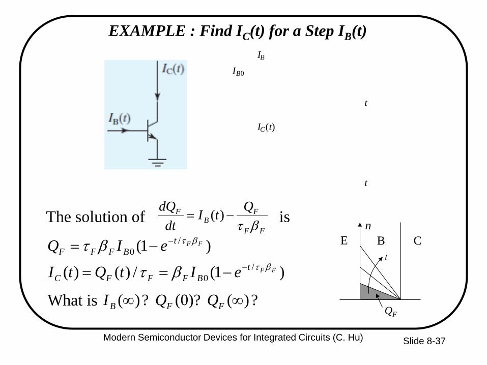
Slide 8-37
EXAMPLE : Find IC(t) for a Step IB(t)
The solution of is FF
FB
F QtIdt
dQβτ
−= )(
)1(/)()(
)1(/
0
/0
FF
FF
tBFFFC
tBFFF
eItQtI
eIQβτ
βτ
βτ
βτ−
−
−==
−=
What is ?)( )?0( ?)( ∞∞ FFB QQI
IB(t)
IC(t)
IC(t)
t
t
IB IB0
E B C n
t
QF
Modern Semiconductor Devices for Integrated Circuits (C. Hu)

Slide 8-38
8.11 Model for Large-Signal Circuit Simulation
• Compact (SPICE) model contains dozens of parameters, mostly determined from measured BJT data.
• Circuits containing tens of thousands of transistors can be simulated.
• Compact model is a “contract” between device/manufacturing engineers and
circuit designers.
)1(1)( /// −−
+−′= kTqV
F
S
A
CBkTqVkTqVSC
BCBCBE eIVVeeII
β
C
B
E
QF
CCS
rB
rC
rE
CBE
QRCBC
IC
Modern Semiconductor Devices for Integrated Circuits (C. Hu)

Slide 8-39
A commonly used BJT compact model is the Gummel-Poon model, consisting of •Ebers-Moll model •Current-dependent beta •Early effect •Transit times •Kirk effect • Voltage-dependent capacitances • Parasitic resistances •Other effects
8.11 Model for Large-Signal Circuit Simulation
Modern Semiconductor Devices for Integrated Circuits (C. Hu)

Slide 8-40
8.12 Chapter Summary
• The base-emitter junction is usually forward-biased while the base-collector is reverse-biased. VBE determines the collector current, IC .
∫≡
−=
B
BE
W
BiB
iB
kTqV
B
iEC
dxDp
nnG
eGqnAI
02
2
/2
)1(
• GB is the base Gummel number, which represents all the subtleties of BJT design that affect IC.
Modern Semiconductor Devices for Integrated Circuits (C. Hu)

Slide 8-41
8.12 Chapter Summary • The base (input) current, IB , is related to IC by the
common-emitter current gain, βF . This can be related to the common-base current gain, αF .
B
E
B
CF G
GII
≈=β
• The Gummel plot shows that βF falls off in the high IC region due to high-level injection in the base. It also falls off in the low IC region due to excess base current.
F
F
E
CF I
Iβ
βα+
==1
• Base-width modulation by VCB results in a significant slope of the IC vs. VCE curve in the active region (known as the Early effect).
Modern Semiconductor Devices for Integrated Circuits (C. Hu)

Slide 8-42
8.12 Chapter Summary • Due to the forward bias VBE , a BJT stores a certain amount
of excess carrier charge QF which is proportional to IC.
FCF IQ τ≡
τF is the forward transit time. If no excess carriers are stored outside the base, then
• The charge-control model first calculates QF(t) from IB(t) and then calculates IC(t).
B
BFBF D
W2
2
== ττ
FF
FB
F QtIdt
dQβτ
−= )(
FFC tQtI τ/)()( =
, the base transit time.
Modern Semiconductor Devices for Integrated Circuits (C. Hu)

Slide 8-43
8.12 Chapter Summary
The small-signal models employ parameters such as transconductance,
qkTI
dVdIg C
BE
Cm /=≡
input capacitance,
and input resistance.
mFBE
F gdVdQC τπ ==
mFB
BE gdI
dVr /βπ ==
Modern Semiconductor Devices for Integrated Circuits (C. Hu)