CC1350 SimpleLink™ Ultra-Low-Power Dual-Band Wireless MCU
75
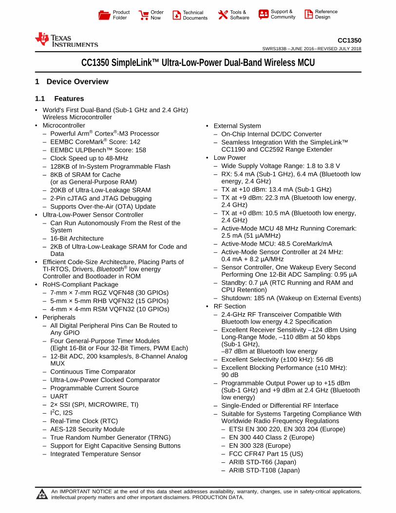
Product Folder Order Now Technical Documents Tools & Software Support & Community Reference Design An IMPORTANT NOTICE at the end of this data sheet addresses availability, warranty, changes, use in safety-critical applications, intellectual property matters and other important disclaimers. PRODUCTION DATA. CC1350 SWRS183B – JUNE 2016 – REVISED JULY 2018 CC1350 SimpleLink™ Ultra-Low-Power Dual-Band Wireless MCU 1 Device Overview 1 1.1 Features 1 • World's First Dual-Band (Sub-1 GHz and 2.4 GHz) Wireless Microcontroller • Microcontroller – Powerful Arm ® Cortex ® -M3 Processor – EEMBC CoreMark ® Score: 142 – EEMBC ULPBench™ Score: 158 – Clock Speed up to 48-MHz – 128KB of In-System Programmable Flash – 8KB of SRAM for Cache (or as General-Purpose RAM) – 20KB of Ultra-Low-Leakage SRAM – 2-Pin cJTAG and JTAG Debugging – Supports Over-the-Air (OTA) Update • Ultra-Low-Power Sensor Controller – Can Run Autonomously From the Rest of the System – 16-Bit Architecture – 2KB of Ultra-Low-Leakage SRAM for Code and Data • Efficient Code-Size Architecture, Placing Parts of TI-RTOS, Drivers, Bluetooth ® low energy Controller and Bootloader in ROM • RoHS-Compliant Package – 7-mm × 7-mm RGZ VQFN48 (30 GPIOs) – 5-mm × 5-mm RHB VQFN32 (15 GPIOs) – 4-mm × 4-mm RSM VQFN32 (10 GPIOs) • Peripherals – All Digital Peripheral Pins Can Be Routed to Any GPIO – Four General-Purpose Timer Modules (Eight 16-Bit or Four 32-Bit Timers, PWM Each) – 12-Bit ADC, 200 ksamples/s, 8-Channel Analog MUX – Continuous Time Comparator – Ultra-Low-Power Clocked Comparator – Programmable Current Source – UART – 2× SSI (SPI, MICROWIRE, TI) –I 2 C, I2S – Real-Time Clock (RTC) – AES-128 Security Module – True Random Number Generator (TRNG) – Support for Eight Capacitive Sensing Buttons – Integrated Temperature Sensor SPACER SPACER SPACER SPACER • External System – On-Chip Internal DC/DC Converter – Seamless Integration With the SimpleLink™ CC1190 and CC2592 Range Extender • Low Power – Wide Supply Voltage Range: 1.8 to 3.8 V – RX: 5.4 mA (Sub-1 GHz), 6.4 mA (Bluetooth low energy, 2.4 GHz) – TX at +10 dBm: 13.4 mA (Sub-1 GHz) – TX at +9 dBm: 22.3 mA (Bluetooth low energy, 2.4 GHz) – TX at +0 dBm: 10.5 mA (Bluetooth low energy, 2.4 GHz) – Active-Mode MCU 48 MHz Running Coremark: 2.5 mA (51 μA/MHz) – Active-Mode MCU: 48.5 CoreMark/mA – Active-Mode Sensor Controller at 24 MHz: 0.4 mA + 8.2 μA/MHz – Sensor Controller, One Wakeup Every Second Performing One 12-Bit ADC Sampling: 0.95 μA – Standby: 0.7 μA (RTC Running and RAM and CPU Retention) – Shutdown: 185 nA (Wakeup on External Events) • RF Section – 2.4-GHz RF Transceiver Compatible With Bluetooth low energy 4.2 Specification – Excellent Receiver Sensitivity –124 dBm Using Long-Range Mode, –110 dBm at 50 kbps (Sub-1 GHz), –87 dBm at Bluetooth low energy – Excellent Selectivity (±100 kHz): 56 dB – Excellent Blocking Performance (±10 MHz): 90 dB – Programmable Output Power up to +15 dBm (Sub-1 GHz) and +9 dBm at 2.4 GHz (Bluetooth low energy) – Single-Ended or Differential RF Interface – Suitable for Systems Targeting Compliance With Worldwide Radio Frequency Regulations – ETSI EN 300 220, EN 303 204 (Europe) – EN 300 440 Class 2 (Europe) – EN 300 328 (Europe) – FCC CFR47 Part 15 (US) – ARIB STD-T66 (Japan) – ARIB STD-T108 (Japan)
Transcript of CC1350 SimpleLink™ Ultra-Low-Power Dual-Band Wireless MCU
Product
Folder
Order
Now
Technical
Documents
Tools &
Software
Support &Community
ReferenceDesign
An IMPORTANT NOTICE at the end of this data sheet addresses availability, warranty, changes, use in safety-critical applications,intellectual property matters and other important disclaimers. PRODUCTION DATA.
CC1350SWRS183B –JUNE 2016–REVISED JULY 2018
CC1350 SimpleLink™ Ultra-Low-Power Dual-Band Wireless MCU
1 Device Overview
1
1.1 Features1
• World's First Dual-Band (Sub-1 GHz and 2.4 GHz)Wireless Microcontroller
• Microcontroller– Powerful Arm® Cortex®-M3 Processor– EEMBC CoreMark® Score: 142– EEMBC ULPBench™ Score: 158– Clock Speed up to 48-MHz– 128KB of In-System Programmable Flash– 8KB of SRAM for Cache
(or as General-Purpose RAM)– 20KB of Ultra-Low-Leakage SRAM– 2-Pin cJTAG and JTAG Debugging– Supports Over-the-Air (OTA) Update
• Ultra-Low-Power Sensor Controller– Can Run Autonomously From the Rest of the
System– 16-Bit Architecture– 2KB of Ultra-Low-Leakage SRAM for Code and
Data• Efficient Code-Size Architecture, Placing Parts of
TI-RTOS, Drivers, Bluetooth® low energyController and Bootloader in ROM
• RoHS-Compliant Package– 7-mm × 7-mm RGZ VQFN48 (30 GPIOs)– 5-mm × 5-mm RHB VQFN32 (15 GPIOs)– 4-mm × 4-mm RSM VQFN32 (10 GPIOs)
• Peripherals– All Digital Peripheral Pins Can Be Routed to
Any GPIO– Four General-Purpose Timer Modules
(Eight 16-Bit or Four 32-Bit Timers, PWM Each)– 12-Bit ADC, 200 ksamples/s, 8-Channel Analog
MUX– Continuous Time Comparator– Ultra-Low-Power Clocked Comparator– Programmable Current Source– UART– 2× SSI (SPI, MICROWIRE, TI)– I2C, I2S– Real-Time Clock (RTC)– AES-128 Security Module– True Random Number Generator (TRNG)– Support for Eight Capacitive Sensing Buttons– Integrated Temperature SensorSPACERSPACER
SPACERSPACER
• External System– On-Chip Internal DC/DC Converter– Seamless Integration With the SimpleLink™
CC1190 and CC2592 Range Extender• Low Power
– Wide Supply Voltage Range: 1.8 to 3.8 V– RX: 5.4 mA (Sub-1 GHz), 6.4 mA (Bluetooth low
energy, 2.4 GHz)– TX at +10 dBm: 13.4 mA (Sub-1 GHz)– TX at +9 dBm: 22.3 mA (Bluetooth low energy,
2.4 GHz)– TX at +0 dBm: 10.5 mA (Bluetooth low energy,
2.4 GHz)– Active-Mode MCU 48 MHz Running Coremark:
2.5 mA (51 µA/MHz)– Active-Mode MCU: 48.5 CoreMark/mA– Active-Mode Sensor Controller at 24 MHz:
0.4 mA + 8.2 µA/MHz– Sensor Controller, One Wakeup Every Second
Performing One 12-Bit ADC Sampling: 0.95 µA– Standby: 0.7 µA (RTC Running and RAM and
CPU Retention)– Shutdown: 185 nA (Wakeup on External Events)
• RF Section– 2.4-GHz RF Transceiver Compatible With
Bluetooth low energy 4.2 Specification– Excellent Receiver Sensitivity –124 dBm Using
Long-Range Mode, –110 dBm at 50 kbps(Sub-1 GHz),–87 dBm at Bluetooth low energy
– Excellent Selectivity (±100 kHz): 56 dB– Excellent Blocking Performance (±10 MHz):
90 dB– Programmable Output Power up to +15 dBm
(Sub-1 GHz) and +9 dBm at 2.4 GHz (Bluetoothlow energy)
– Single-Ended or Differential RF Interface– Suitable for Systems Targeting Compliance With
Worldwide Radio Frequency Regulations– ETSI EN 300 220, EN 303 204 (Europe)– EN 300 440 Class 2 (Europe)– EN 300 328 (Europe)– FCC CFR47 Part 15 (US)– ARIB STD-T66 (Japan)– ARIB STD-T108 (Japan)

2
CC1350SWRS183B –JUNE 2016–REVISED JULY 2018 www.ti.com
Submit Documentation FeedbackProduct Folder Links: CC1350
Device Overview Copyright © 2016–2018, Texas Instruments Incorporated
– Wireless M-Bus (EN 13757-4) and IEEE®
802.15.4g PHY• Tools and Development Environment
– Full-Feature and Low-Cost Development Kits– Multiple Reference Designs for Different RF
Configurations– Packet Sniffer PC Software
– Sensor Controller Studio– SmartRF™ Studio– SmartRF Flash Programmer 2– IAR Embedded Workbench® for Arm– Code Composer Studio™ (CCS) IDE– CCS UniFlash
1.2 Applications• 315-, 433-, 470-, 500-, 779-, 868-, 915-,
920-MHz and 2.4-GHz ISM and SRD Systems• Low-Power Wireless Systems
With 50-kHz to 5-MHz Channel Spacing• Home and Building Automation• Wireless Alarm and Security Systems• Industrial Monitoring and Control• Bluetooth low energy Beacon Management• Bluetooth low energy Commissioning• Smart Grid and Automatic Meter Reading
• Wireless Healthcare Applications• Wireless Sensor Networks• Active RFID• IEEE 802.15.4g, IP-Enabled Smart Objects
(6LoWPAN), Wireless M-Bus, KNX Systems,Wi-SUN™, and Proprietary Systems
• Energy-Harvesting Applications• Electronic Shelf Label (ESL)• Long-Range Sensor Applications• Heat-Cost Allocators
1.3 DescriptionThe CC1350 device is a cost-effective, ultra-low-power, dual-band RF device from Texas Instruments™that is part of the SimpleLink™ microcontroller (MCU) platform. The platform consists of Wi-Fi®, Bluetooth®
low energy, Sub-1 GHz, Ethernet, Zigbee®, Thread, and host MCUs. These devices all share a common,easy-to-use development environment with a single core software development kit (SDK) and a rich toolset. A one-time integration of the SimpleLink platform enables users to add any combination of devicesfrom the portfolio into their design, allowing 100 percent code reuse when design requirements change.For more information, visit www.ti.com/simplelink.
With very low active RF and MCU current consumption, in addition to flexible low-power modes, thedevice provides excellent battery life and allows long-range operation on small coin-cell batteries and inenergy harvesting applications.
The CC1350 is a device in the CC13xx and CC26xx family of cost-effective, ultra-low-power wirelessMCUs capable of handling both Sub-1 GHz and 2.4-GHz RF frequencies. The CC1350 device combines aflexible, very low-power RF transceiver with a powerful 48-MHz Arm® Cortex®-M3 microcontroller in aplatform supporting multiple physical layers and RF standards. A dedicated Radio Controller (Cortex®-M0)handles low-level RF protocol commands that are stored in ROM or RAM, thus ensuring ultra-low powerand flexibility to handle both Sub-1 GHz protocols and 2.4 GHz protocols (for example Bluetooth lowenergy). This enables the combination of a Sub-1 GHz communication solution that offers the bestpossible RF range together with a Bluetooth low energy smartphone connection that enables great userexperience through a phone application. The Sub-1 GHz only device in this family is the CC1310.
The CC1350 device is a highly integrated, true single-chip solution incorporating a complete RF systemand an on-chip DC/DC converter.
Sensors can be handled in a very low-power manner by a dedicated autonomous ultra-low-power MCUthat can be configured to handle analog and digital sensors; thus the main MCU (Arm® Cortex®-M3) canmaximize sleep time.
The power and clock management and radio systems of the CC1350 device require specific configurationand handling by software to operate correctly, which has been implemented in the TI-RTOS. TIrecommends using this software framework for all application development on the device. The completeTI-RTOS and device drivers are offered free of charge in source code.
3
CC1350www.ti.com SWRS183B –JUNE 2016–REVISED JULY 2018
Submit Documentation FeedbackProduct Folder Links: CC1350
Device OverviewCopyright © 2016–2018, Texas Instruments Incorporated
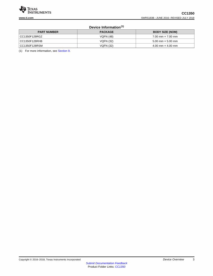
(1) For more information, see Section 9.
Device Information (1)
PART NUMBER PACKAGE BODY SIZE (NOM)CC1350F128RGZ VQFN (48) 7.00 mm × 7.00 mmCC1350F128RHB VQFN (32) 5.00 mm × 5.00 mmCC1350F128RSM VQFN (32) 4.00 mm × 4.00 mm
SimpleLink TM CC1350 Wireless MCU
Main CPU:
128-KBFlash
Sensor Controller
cJTAG
20-KBSRAM
ROM
ARM®
Cortex ®-M3
DC-DC Converter
RF core
ARM®
Cortex ®-M0
DSP Modem
4-KB SRAM
ROM
Sensor Controller Engine
2x Analog Comparators
12-Bit ADC, 200ks/s
Constant Current Source
SPI / I2C Digital Sensor IF
2-KB SRAM
Time-to-Digital Converter
General Peripherals / Modules
2x SSI (SPI,µW,TI)
Watchdog Timer
Temp. / Batt. Monitor
RTC
I2C
UART
I2S
10 / 15 / 30 GPIOs
AES
32 ch. PDMA
ADC
ADC
Digital PLL
TRNG
8-KBCache
4x 32-Bit Timers
Copyright © 2016, Texas Instruments Incorporated
4
CC1350SWRS183B –JUNE 2016–REVISED JULY 2018 www.ti.com
Submit Documentation FeedbackProduct Folder Links: CC1350
Device Overview Copyright © 2016–2018, Texas Instruments Incorporated
1.4 Functional Block DiagramFigure 1-1 shows a block diagram for the CC1350 device.
Figure 1-1. CC1350 Block Diagram
5
CC1350www.ti.com SWRS183B –JUNE 2016–REVISED JULY 2018
Submit Documentation FeedbackProduct Folder Links: CC1350
Table of ContentsCopyright © 2016–2018, Texas Instruments Incorporated
Table of Contents1 Device Overview ......................................... 1
1.1 Features .............................................. 11.2 Applications........................................... 21.3 Description............................................ 21.4 Functional Block Diagram ............................ 4
2 Revision History ......................................... 63 Device Comparison ..................................... 7
3.1 Related Products ..................................... 74 Terminal Configuration and Functions.............. 8
4.1 Pin Diagram – RSM Package ........................ 84.2 Signal Descriptions – RSM Package................. 94.3 Pin Diagram – RHB Package ....................... 104.4 Signal Descriptions – RHB Package................ 114.5 Pin Diagram – RGZ Package ....................... 124.6 Signal Descriptions – RGZ Package................ 13
5 Specifications ........................................... 155.1 Absolute Maximum Ratings ......................... 155.2 ESD Ratings ........................................ 155.3 Recommended Operating Conditions............... 155.4 Power Consumption Summary...................... 165.5 RF Characteristics .................................. 175.6 Receive (RX) Parameters, 861 MHz to 1054 MHz . 175.7 Receive (RX) Parameters, 431 MHz to 527 MHz .. 235.8 Transmit (TX) Parameters, 861 MHz to 1054 MHz . 255.9 Transmit (TX) Parameters, 431 MHz to 527 MHz .. 265.10 1-Mbps GFSK (Bluetooth low energy) – RX ........ 265.11 1-Mbps GFSK (Bluetooth low energy) – TX ........ 275.12 PLL Parameters..................................... 285.13 ADC Characteristics................................. 285.14 Temperature Sensor ................................ 295.15 Battery Monitor ...................................... 295.16 Continuous Time Comparator....................... 305.17 Low-Power Clocked Comparator ................... 305.18 Programmable Current Source ..................... 30
5.19 DC Characteristics .................................. 315.20 Thermal Characteristics ............................. 325.21 Timing and Switching Characteristics ............... 325.22 Typical Characteristics .............................. 365.23 Typical Characteristics – Sub-1 GHz ............... 375.24 Typical Characteristics – 2.4 GHz .................. 42
6 Detailed Description ................................... 446.1 Overview ............................................ 446.2 Main CPU ........................................... 446.3 RF Core ............................................. 456.4 Sensor Controller ................................... 466.5 Memory.............................................. 476.6 Debug ............................................... 476.7 Power Management................................. 486.8 Clock Systems ...................................... 496.9 General Peripherals and Modules .................. 496.10 Voltage Supply Domains ............................ 506.11 System Architecture................................. 50
7 Application, Implementation, and Layout ......... 517.1 Application Information.............................. 517.2 TI Design or Reference Design ..................... 52
8 Device and Documentation Support ............... 538.1 Device Nomenclature ............................... 538.2 Tools and Software ................................. 548.3 Documentation Support ............................. 568.4 Texas Instruments Low-Power RF Website ........ 568.5 Additional Information ............................... 568.6 Community Resources .............................. 568.7 Trademarks.......................................... 578.8 Electrostatic Discharge Caution..................... 578.9 Export Control Notice ............................... 578.10 Glossary ............................................. 57
9 Mechanical, Packaging, and OrderableInformation .............................................. 579.1 Packaging Information .............................. 57
6
CC1350SWRS183B –JUNE 2016–REVISED JULY 2018 www.ti.com
Submit Documentation FeedbackProduct Folder Links: CC1350
Revision History Copyright © 2016–2018, Texas Instruments Incorporated
2 Revision HistoryNOTE: Page numbers for previous revisions may differ from page numbers in the current version.
Changes from November 20, 2016 to July 13, 2018 Page
• Changed Description section ....................................................................................................... 2• Changed Table 3-1 ................................................................................................................... 7• Changed test conditions for Receiver sensitivity, 50 kbps in Section 5.6 ................................................... 17• Added parameters to Section 5.6 ................................................................................................. 17• Added Receiver sensitivity parameters to Section 5.7 ......................................................................... 23• Changed ............................................................................................................................. 33• Changed footnote in ................................................................................................................ 33• Added Software section ........................................................................................................... 54
Changes from June 20, 2016 to November 20, 2016 Page
• Added 4-mm × 4-mm and 5-mm × 5-mm packages ............................................................................. 1• Added Figure 4-1 ..................................................................................................................... 8• Added Figure 4-2.................................................................................................................... 10• Added support for split supply rail to Section 5.3 ............................................................................... 15• Added OOK modulation support to Section 5.4 ................................................................................. 16• Added receive parameters for 431-MHz to 527-MHz band in Section 5.7 .................................................. 23• Added transmit parameters for 431-MHz to 527-MHz band in Section 5.9 ................................................. 26• Changed ADC reference voltage to correct value in Section 5.13 ........................................................... 29• Added thermal characteristics for RHB and RSM packages in Section 5.20 ............................................... 32• Added Figure 5-10 .................................................................................................................. 37• Added Section 6.10 ................................................................................................................. 50• Changed Figure 8-1................................................................................................................. 53
7
CC1350www.ti.com SWRS183B –JUNE 2016–REVISED JULY 2018
Submit Documentation FeedbackProduct Folder Links: CC1350
Device ComparisonCopyright © 2016–2018, Texas Instruments Incorporated
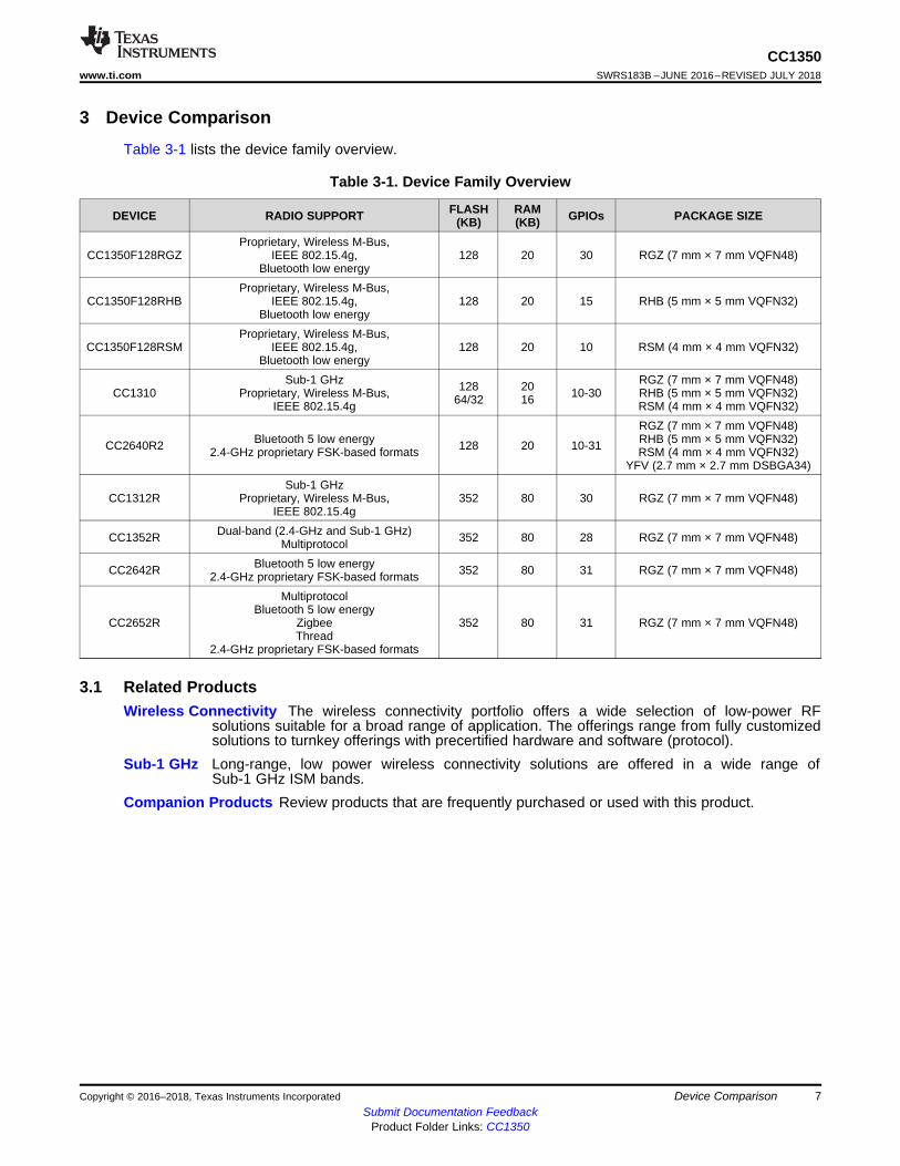
3 Device Comparison
Table 3-1 lists the device family overview.
Table 3-1. Device Family Overview
DEVICE RADIO SUPPORT FLASH(KB)
RAM(KB) GPIOs PACKAGE SIZE
CC1350F128RGZProprietary, Wireless M-Bus,
IEEE 802.15.4g,Bluetooth low energy
128 20 30 RGZ (7 mm × 7 mm VQFN48)
CC1350F128RHBProprietary, Wireless M-Bus,
IEEE 802.15.4g,Bluetooth low energy
128 20 15 RHB (5 mm × 5 mm VQFN32)
CC1350F128RSMProprietary, Wireless M-Bus,
IEEE 802.15.4g,Bluetooth low energy
128 20 10 RSM (4 mm × 4 mm VQFN32)
CC1310Sub-1 GHz
Proprietary, Wireless M-Bus,IEEE 802.15.4g
12864/32
2016 10-30
RGZ (7 mm × 7 mm VQFN48)RHB (5 mm × 5 mm VQFN32)RSM (4 mm × 4 mm VQFN32)
CC2640R2 Bluetooth 5 low energy2.4-GHz proprietary FSK-based formats 128 20 10-31
RGZ (7 mm × 7 mm VQFN48)RHB (5 mm × 5 mm VQFN32)RSM (4 mm × 4 mm VQFN32)
YFV (2.7 mm × 2.7 mm DSBGA34)
CC1312RSub-1 GHz
Proprietary, Wireless M-Bus,IEEE 802.15.4g
352 80 30 RGZ (7 mm × 7 mm VQFN48)
CC1352R Dual-band (2.4-GHz and Sub-1 GHz)Multiprotocol 352 80 28 RGZ (7 mm × 7 mm VQFN48)
CC2642R Bluetooth 5 low energy2.4-GHz proprietary FSK-based formats 352 80 31 RGZ (7 mm × 7 mm VQFN48)
CC2652R
MultiprotocolBluetooth 5 low energy
ZigbeeThread
2.4-GHz proprietary FSK-based formats
352 80 31 RGZ (7 mm × 7 mm VQFN48)
3.1 Related ProductsWireless Connectivity The wireless connectivity portfolio offers a wide selection of low-power RF
solutions suitable for a broad range of application. The offerings range from fully customizedsolutions to turnkey offerings with precertified hardware and software (protocol).
Sub-1 GHz Long-range, low power wireless connectivity solutions are offered in a wide range ofSub-1 GHz ISM bands.
Companion Products Review products that are frequently purchased or used with this product.

28
29
27
3021 2022 19 18
13
12
14
114 53 6 7
26 15
25 16
31 10
32 9
232
241
178
DIO
_6
VS
S
DIO
_5
RE
SE
T_N
VS
S
VD
DS
_DC
DC
DC
DC
_SW
DIO
_7
VDDR_RF
X24M_P
X24M_N
VSS
VDDR
DIO_9
VDDS
DIO_8
DIO_1
JTAG_TCKC
DIO_2
JTAG_TMSC
VDDS2
DIO_3
DIO_4
RF
_P
RF
_N
VS
S
X32
K_Q
2
VS
S
DIO
_0
RX
_TX
X32
K_Q
1
DCOUPL
8
CC1350SWRS183B –JUNE 2016–REVISED JULY 2018 www.ti.com
Submit Documentation FeedbackProduct Folder Links: CC1350
Terminal Configuration and Functions Copyright © 2016–2018, Texas Instruments Incorporated
4 Terminal Configuration and Functions
4.1 Pin Diagram – RSM PackageFigure 4-1 shows the RSM pinout diagram.
Figure 4-1. RSM (4-mm × 4-mm) Pinout, 0.4-mm PitchTop View
I/O pins marked in Figure 4-1 in bold have high-drive capabilities; they are as follows:• Pin 8, DIO_0• Pin 9, DIO_1• Pin 10, DIO_2• Pin 13, JTAG_TMSC• Pin 15, DIO_3• Pin 16, DIO_4
I/O pins marked in Figure 4-1 in italics have analog capabilities; they are as follows:• Pin 22, DIO_5• Pin 23, DIO_6• Pin 24, DIO_7• Pin 25, DIO_8• Pin 26, DIO_9
9
CC1350www.ti.com SWRS183B –JUNE 2016–REVISED JULY 2018
Submit Documentation FeedbackProduct Folder Links: CC1350
Terminal Configuration and FunctionsCopyright © 2016–2018, Texas Instruments Incorporated
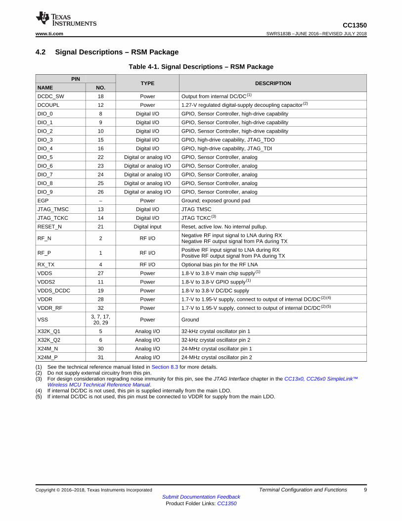
(1) See the technical reference manual listed in Section 8.3 for more details.(2) Do not supply external circuitry from this pin.(3) For design consideration regrading noise immunity for this pin, see the JTAG Interface chapter in the CC13x0, CC26x0 SimpleLink™
Wireless MCU Technical Reference Manual.(4) If internal DC/DC is not used, this pin is supplied internally from the main LDO.(5) If internal DC/DC is not used, this pin must be connected to VDDR for supply from the main LDO.
4.2 Signal Descriptions – RSM Package
Table 4-1. Signal Descriptions – RSM Package
PINTYPE DESCRIPTION
NAME NO.DCDC_SW 18 Power Output from internal DC/DC (1)
DCOUPL 12 Power 1.27-V regulated digital-supply decoupling capacitor (2)
DIO_0 8 Digital I/O GPIO, Sensor Controller, high-drive capabilityDIO_1 9 Digital I/O GPIO, Sensor Controller, high-drive capabilityDIO_2 10 Digital I/O GPIO, Sensor Controller, high-drive capabilityDIO_3 15 Digital I/O GPIO, high-drive capability, JTAG_TDODIO_4 16 Digital I/O GPIO, high-drive capability, JTAG_TDIDIO_5 22 Digital or analog I/O GPIO, Sensor Controller, analogDIO_6 23 Digital or analog I/O GPIO, Sensor Controller, analogDIO_7 24 Digital or analog I/O GPIO, Sensor Controller, analogDIO_8 25 Digital or analog I/O GPIO, Sensor Controller, analogDIO_9 26 Digital or analog I/O GPIO, Sensor Controller, analogEGP – Power Ground; exposed ground padJTAG_TMSC 13 Digital I/O JTAG TMSCJTAG_TCKC 14 Digital I/O JTAG TCKC (3)
RESET_N 21 Digital input Reset, active low. No internal pullup.
RF_N 2 RF I/O Negative RF input signal to LNA during RXNegative RF output signal from PA during TX
RF_P 1 RF I/O Positive RF input signal to LNA during RXPositive RF output signal from PA during TX
RX_TX 4 RF I/O Optional bias pin for the RF LNAVDDS 27 Power 1.8-V to 3.8-V main chip supply (1)
VDDS2 11 Power 1.8-V to 3.8-V GPIO supply (1)
VDDS_DCDC 19 Power 1.8-V to 3.8-V DC/DC supplyVDDR 28 Power 1.7-V to 1.95-V supply, connect to output of internal DC/DC (2) (4)
VDDR_RF 32 Power 1.7-V to 1.95-V supply, connect to output of internal DC/DC (2) (5)
VSS 3, 7, 17,20, 29 Power Ground
X32K_Q1 5 Analog I/O 32-kHz crystal oscillator pin 1X32K_Q2 6 Analog I/O 32-kHz crystal oscillator pin 2X24M_N 30 Analog I/O 24-MHz crystal oscillator pin 1X24M_P 31 Analog I/O 24-MHz crystal oscillator pin 2
28
29
27
30
21 2022 19 18
13
12
14
11
4 53 6 7
26 15
25 16
31 10
32 9
232
241
178
DIO
_10
DIO
_7
DIO
_9
DIO
_8
DC
DC
_SW
RE
SE
T_N
VD
DS
_DC
DC
DIO
_11
VDDR_RF
X24M_P
X24M_N
VDDR
VDDS
DIO_13
DIO_14
DIO_12
DIO_3
JTAG_TCKC
DIO_4
JTAG_TMSC
VDDS2
DIO_5
DIO_6
RF
_P
RF
_N
RX
_TX
DIO
_0
DIO
_1
DIO
_2
X32
K_Q
1
X32
K_Q
2
DCOUPL
10
CC1350SWRS183B –JUNE 2016–REVISED JULY 2018 www.ti.com
Submit Documentation FeedbackProduct Folder Links: CC1350
Terminal Configuration and Functions Copyright © 2016–2018, Texas Instruments Incorporated
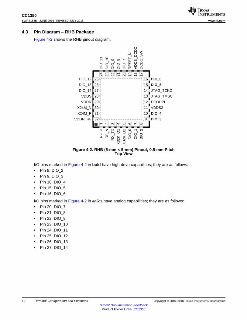
4.3 Pin Diagram – RHB PackageFigure 4-2 shows the RHB pinout diagram.
Figure 4-2. RHB (5-mm × 5-mm) Pinout, 0.5-mm PitchTop View
I/O pins marked in Figure 4-2 in bold have high-drive capabilities; they are as follows:• Pin 8, DIO_2• Pin 9, DIO_3• Pin 10, DIO_4• Pin 15, DIO_5• Pin 16, DIO_6
I/O pins marked in Figure 4-2 in italics have analog capabilities; they are as follows:• Pin 20, DIO_7• Pin 21, DIO_8• Pin 22, DIO_9• Pin 23, DIO_10• Pin 24, DIO_11• Pin 25, DIO_12• Pin 26, DIO_13• Pin 27, DIO_14

11
CC1350www.ti.com SWRS183B –JUNE 2016–REVISED JULY 2018
Submit Documentation FeedbackProduct Folder Links: CC1350
Terminal Configuration and FunctionsCopyright © 2016–2018, Texas Instruments Incorporated
(1) For more details, see the technical reference manual listed in Section 8.3.(2) Do not supply external circuitry from this pin.(3) For design consideration regrading noise immunity for this pin, see the JTAG Interface chapter in the CC13x0, CC26x0 SimpleLink™
Wireless MCU Technical Reference Manual.(4) If internal DC/DC is not used, this pin is supplied internally from the main LDO.(5) If internal DC/DC is not used, this pin must be connected to VDDR for supply from the main LDO.
4.4 Signal Descriptions – RHB Package
Table 4-2. Signal Descriptions – RHB Package
PINTYPE DESCRIPTION
NAME NO.DCDC_SW 17 Power Output from internal DC/DC (1)
DCOUPL 12 Power 1.27-V regulated digital-supply decoupling (2)
DIO_0 6 Digital I/O GPIO, Sensor ControllerDIO_1 7 Digital I/O GPIO, Sensor ControllerDIO_2 8 Digital I/O GPIO, Sensor Controller, high-drive capabilityDIO_3 9 Digital I/O GPIO, Sensor Controller, high-drive capabilityDIO_4 10 Digital I/O GPIO, Sensor Controller, high-drive capabilityDIO_5 15 Digital I/O GPIO, high-drive capability, JTAG_TDODIO_6 16 Digital I/O GPIO, high-drive capability, JTAG_TDIDIO_7 20 Digital or analog I/O GPIO, Sensor Controller, analogDIO_8 21 Digital or analog I/O GPIO, Sensor Controller, analogDIO_9 22 Digital or analog I/O GPIO, Sensor Controller, analogDIO_10 23 Digital or analog I/O GPIO, Sensor Controller, AnalogDIO_11 24 Digital or analog I/O GPIO, Sensor Controller, analogDIO_12 25 Digital or analog I/O GPIO, Sensor Controller, analogDIO_13 26 Digital or analog I/O GPIO, Sensor Controller, analogDIO_14 27 Digital or analog I/O GPIO, Sensor Controller, analogEGP – Power Ground; exposed ground padJTAG_TMSC 13 Digital I/O JTAG TMSC, high-drive capabilityJTAG_TCKC 14 Digital I/O JTAG TCKC (3)
RESET_N 19 Digital input Reset, active low. No internal pullup.
RF_N 2 RF I/O Negative RF input signal to LNA during RXNegative RF output signal from PA during TX
RF_P 1 RF I/O Positive RF input signal to LNA during RXPositive RF output signal from PA during TX
RX_TX 3 RF I/O Optional bias pin for the RF LNAVDDR 29 Power 1.7-V to 1.95-V supply, connect to output of internal DC/DC (2) (4)
VDDR_RF 32 Power 1.7-V to 1.95-V supply, connect to output of internal DC/DC (2) (5)
VDDS 28 Power 1.8-V to 3.8-V main chip supply (1)
VDDS2 11 Power 1.8-V to 3.8-V GPIO supply (1)
VDDS_DCDC 18 Power 1.8-V to 3.8-V DC/DC supplyX24M_N 30 Analog I/O 24-MHz crystal oscillator pin 1X24M_P 31 Analog I/O 24-MHz crystal oscillator pin 2X32K_Q1 4 Analog I/O 32-kHz crystal oscillator pin 1X32K_Q2 5 Analog I/O 32-kHz crystal oscillator pin 2
40
39
DIO_24
38
37
21
22
23
24
DC
DC
_SW
3334
RE
SE
T_N
35
DIO
_23
36
X32
K_Q
2
4X
32K
_Q1
3
RF
_N2
RF
_P1
DIO
_21
32
DIO
_20
31
DIO
_19
30
DIO
_18
29
5
DIO
_16
DIO
_27 8
28 27 26
JTA
G_T
CK
C25
9 10 11 12
41
42
43
44
20 DIO_14
19 DIO_13
18
17
VDDR 45
46
47
VDDR_RF 48
16
15
14
13D
IO_1
7
DIO
_16
VD
DS
_DC
DC
DIO_25
DIO_11
DIO_12
VDDS2
DIO_10
DIO_9
DIO
_5
DIO
_6
DIO
_7
DIO
_3
DIO
_4X24M_N
X24M_P DIO_8
DIO_27
VDDS3
DCOUPL
JTAG_TMSC
DIO_28
DIO_26
VDDS
RX
_TX
DIO_29
DIO_15
DIO
_22
DIO_30
12
CC1350SWRS183B –JUNE 2016–REVISED JULY 2018 www.ti.com
Submit Documentation FeedbackProduct Folder Links: CC1350
Terminal Configuration and Functions Copyright © 2016–2018, Texas Instruments Incorporated
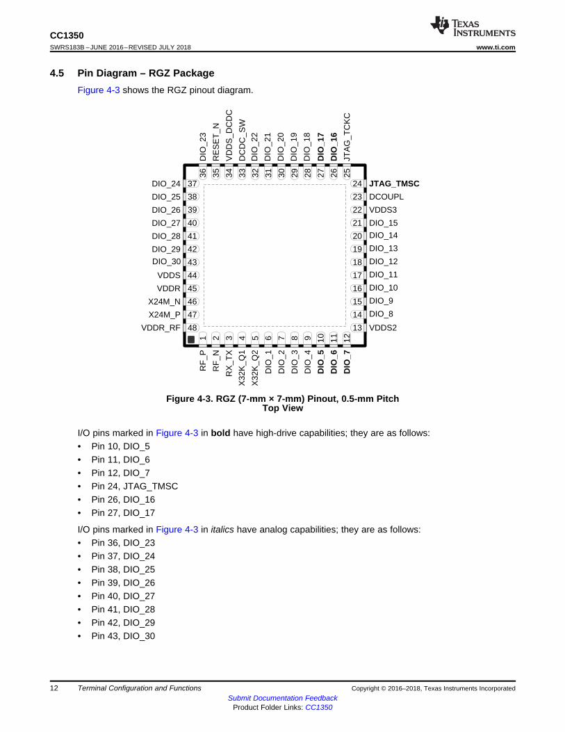
4.5 Pin Diagram – RGZ PackageFigure 4-3 shows the RGZ pinout diagram.
Figure 4-3. RGZ (7-mm × 7-mm) Pinout, 0.5-mm PitchTop View
I/O pins marked in Figure 4-3 in bold have high-drive capabilities; they are as follows:• Pin 10, DIO_5• Pin 11, DIO_6• Pin 12, DIO_7• Pin 24, JTAG_TMSC• Pin 26, DIO_16• Pin 27, DIO_17
I/O pins marked in Figure 4-3 in italics have analog capabilities; they are as follows:• Pin 36, DIO_23• Pin 37, DIO_24• Pin 38, DIO_25• Pin 39, DIO_26• Pin 40, DIO_27• Pin 41, DIO_28• Pin 42, DIO_29• Pin 43, DIO_30
13
CC1350www.ti.com SWRS183B –JUNE 2016–REVISED JULY 2018
Submit Documentation FeedbackProduct Folder Links: CC1350
Terminal Configuration and FunctionsCopyright © 2016–2018, Texas Instruments Incorporated
(1) See technical reference manual listed in Section 8.3 for more details.(2) Do not supply external circuitry from this pin.(3) For design consideration regrading noise immunity for this pin, see the JTAG Interface chapter in the CC13x0, CC26x0 SimpleLink™
Wireless MCU Technical Reference Manual.
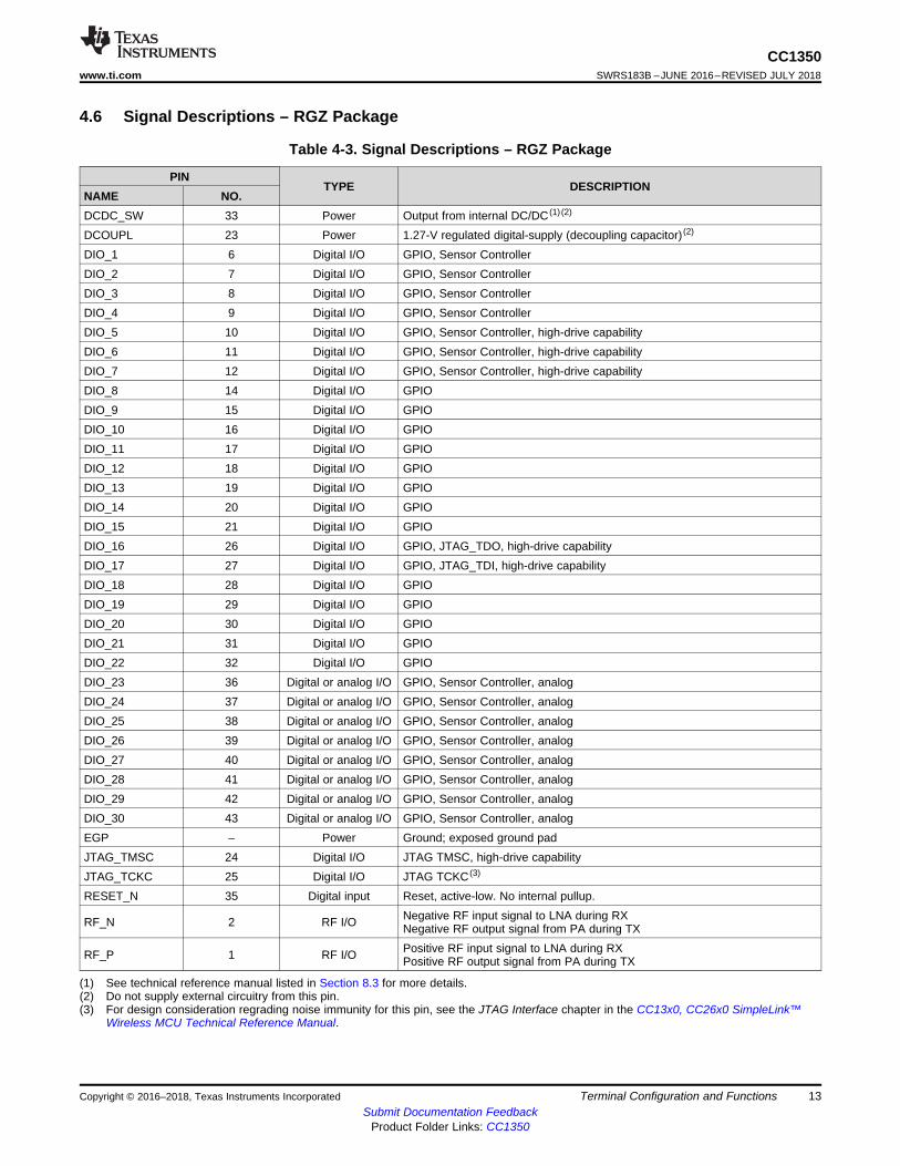
4.6 Signal Descriptions – RGZ Package
Table 4-3. Signal Descriptions – RGZ Package
PINTYPE DESCRIPTION
NAME NO.DCDC_SW 33 Power Output from internal DC/DC (1) (2)
DCOUPL 23 Power 1.27-V regulated digital-supply (decoupling capacitor) (2)
DIO_1 6 Digital I/O GPIO, Sensor ControllerDIO_2 7 Digital I/O GPIO, Sensor ControllerDIO_3 8 Digital I/O GPIO, Sensor ControllerDIO_4 9 Digital I/O GPIO, Sensor ControllerDIO_5 10 Digital I/O GPIO, Sensor Controller, high-drive capabilityDIO_6 11 Digital I/O GPIO, Sensor Controller, high-drive capabilityDIO_7 12 Digital I/O GPIO, Sensor Controller, high-drive capabilityDIO_8 14 Digital I/O GPIODIO_9 15 Digital I/O GPIODIO_10 16 Digital I/O GPIODIO_11 17 Digital I/O GPIODIO_12 18 Digital I/O GPIODIO_13 19 Digital I/O GPIODIO_14 20 Digital I/O GPIODIO_15 21 Digital I/O GPIODIO_16 26 Digital I/O GPIO, JTAG_TDO, high-drive capabilityDIO_17 27 Digital I/O GPIO, JTAG_TDI, high-drive capabilityDIO_18 28 Digital I/O GPIODIO_19 29 Digital I/O GPIODIO_20 30 Digital I/O GPIODIO_21 31 Digital I/O GPIODIO_22 32 Digital I/O GPIODIO_23 36 Digital or analog I/O GPIO, Sensor Controller, analogDIO_24 37 Digital or analog I/O GPIO, Sensor Controller, analogDIO_25 38 Digital or analog I/O GPIO, Sensor Controller, analogDIO_26 39 Digital or analog I/O GPIO, Sensor Controller, analogDIO_27 40 Digital or analog I/O GPIO, Sensor Controller, analogDIO_28 41 Digital or analog I/O GPIO, Sensor Controller, analogDIO_29 42 Digital or analog I/O GPIO, Sensor Controller, analogDIO_30 43 Digital or analog I/O GPIO, Sensor Controller, analogEGP – Power Ground; exposed ground padJTAG_TMSC 24 Digital I/O JTAG TMSC, high-drive capabilityJTAG_TCKC 25 Digital I/O JTAG TCKC (3)
RESET_N 35 Digital input Reset, active-low. No internal pullup.
RF_N 2 RF I/O Negative RF input signal to LNA during RXNegative RF output signal from PA during TX
RF_P 1 RF I/O Positive RF input signal to LNA during RXPositive RF output signal from PA during TX
14
CC1350SWRS183B –JUNE 2016–REVISED JULY 2018 www.ti.com
Submit Documentation FeedbackProduct Folder Links: CC1350
Terminal Configuration and Functions Copyright © 2016–2018, Texas Instruments Incorporated
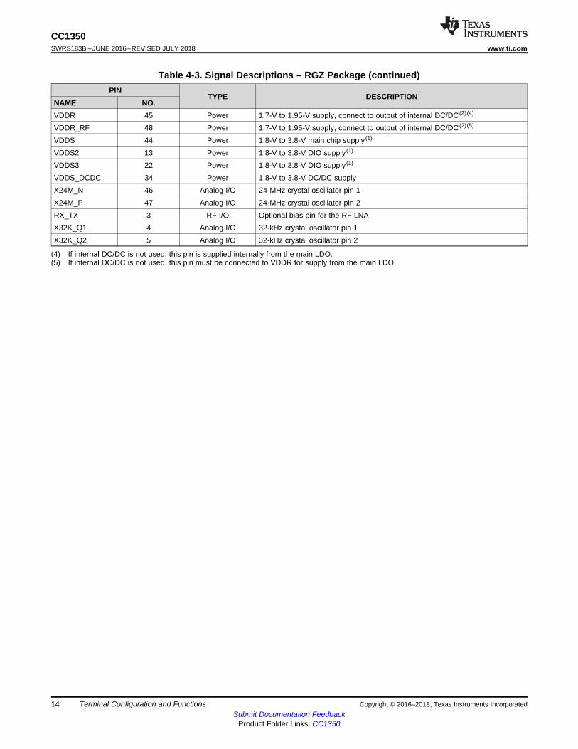
Table 4-3. Signal Descriptions – RGZ Package (continued)PIN
TYPE DESCRIPTIONNAME NO.
(4) If internal DC/DC is not used, this pin is supplied internally from the main LDO.(5) If internal DC/DC is not used, this pin must be connected to VDDR for supply from the main LDO.
VDDR 45 Power 1.7-V to 1.95-V supply, connect to output of internal DC/DC (2) (4)
VDDR_RF 48 Power 1.7-V to 1.95-V supply, connect to output of internal DC/DC (2) (5)
VDDS 44 Power 1.8-V to 3.8-V main chip supply (1)
VDDS2 13 Power 1.8-V to 3.8-V DIO supply (1)
VDDS3 22 Power 1.8-V to 3.8-V DIO supply (1)
VDDS_DCDC 34 Power 1.8-V to 3.8-V DC/DC supplyX24M_N 46 Analog I/O 24-MHz crystal oscillator pin 1X24M_P 47 Analog I/O 24-MHz crystal oscillator pin 2RX_TX 3 RF I/O Optional bias pin for the RF LNAX32K_Q1 4 Analog I/O 32-kHz crystal oscillator pin 1X32K_Q2 5 Analog I/O 32-kHz crystal oscillator pin 2
15
CC1350www.ti.com SWRS183B –JUNE 2016–REVISED JULY 2018
Submit Documentation FeedbackProduct Folder Links: CC1350
SpecificationsCopyright © 2016–2018, Texas Instruments Incorporated
(1) Stresses beyond those listed under Absolute Maximum Ratings may cause permanent damage to the device. These are stress ratingsonly, and functional operation of the device at these or any other conditions beyond those indicated under Recommended OperatingConditions is not implied. Exposure to absolute-maximum-rated conditions for extended periods may affect device reliability.
(2) All voltage values are with respect to ground, unless otherwise noted.(3) Including analog-capable DIO.(4) Each pin is referenced to a specific VDDSn (VDDS, VDDS2 or VDDS3). For a pin-to-VDDS mapping table, see Table 6-3.
5 Specifications
5.1 Absolute Maximum Ratingsover operating free-air temperature range (unless otherwise noted) (1) (2)
MIN MAX UNITSupply voltage (VDDS, VDDS2, and VDDS3) –0.3 4.1 VVoltage on any digital pin (3) (4) –0.3 VDDSn + 0.3, max 4.1 VVoltage on crystal oscillator pins X32K_Q1, X32K_Q2, X24M_N, and X24M_P –0.3 VDDR + 0.3, max 2.25 V
Voltage on ADC input (Vin)Voltage scaling enabled –0.3 VDDS
VVoltage scaling disabled, internal reference –0.3 1.49Voltage scaling disabled, VDDS as reference –0.3 VDDS / 2.9
Input RF level 10 dBmStorage temperature (Tstg) –40 150 °C
(1) JEDEC document JEP155 states that 500-V HBM allows safe manufacturing with a standard ESD control process.(2) JEDEC document JEP157 states that 250-V CDM allows safe manufacturing with a standard ESD control process.
5.2 ESD RatingsVALUE UNIT
VESD Electrostatic dischargeHuman body model (HBM), per ANSI/ESDA/JEDEC JS001 (1) All pins ±3000
VCharged device model (CDM), per JESD22-C101 (2) All pins ±500
(1) For small coin-cell batteries, with high worst-case end-of-life equivalent source resistance, a 22-µF VDDS input capacitor must be usedto ensure compliance with this slew rate.
(2) Applications using RCOSC_LF as sleep timer must also consider the drift in frequency caused by a change in temperature (see ).
5.3 Recommended Operating Conditionsover operating free-air temperature range (unless otherwise noted)
MIN MAX UNITAmbient temperature –40 85 °COperating supply voltage (VDDS) For operation in battery-powered and
3.3-V systems (internal DC/DC can beused to minimize power consumption)
1.8 3.8 VOperating supply voltages (VDDS2 and VDDS3) VDDS < 2.7 V 1.8 3.8 VOperating supply voltages (VDDS2 and VDDS3) VDDS ≥ 2.7 V 1.9 3.8 VRising supply voltage slew rate 0 100 mV/µsFalling supply voltage slew rate 0 20 mV/µsFalling supply voltage slew rate, with low-power flash setting (1) 3 mV/µs
Positive temperature gradient in standby (2) No limitation for negative temperature gradient, or outsidestandby mode 5 °C/s

16
CC1350SWRS183B –JUNE 2016–REVISED JULY 2018 www.ti.com
Submit Documentation FeedbackProduct Folder Links: CC1350
Specifications Copyright © 2016–2018, Texas Instruments Incorporated
5.4 Power Consumption SummaryMeasured on the Texas Instruments CC1310EM-7XD-7793 reference design unless otherwise noted. Tc = 25°C, VDDS = 3.6 Vwith DC/DC enabled, unless otherwise noted. Using boost mode (increasing VDDR to 1.95 V), will increase currents in thistable by 15% (does not apply to TX 14-dBm setting where this current is already included).
PARAMETER TEST CONDITIONS TYP UNIT
IcoreCore currentconsumption
Reset. RESET_N pin asserted or VDDS below power-on-resetthreshold 100
nAShutdown. No clocks running, no retention 185Standby. With RTC, CPU, RAM, and (partial) register retention.RCOSC_LF 0.7
µAStandby. With RTC, CPU, RAM, and (partial) register retention.XOSC_LF 0.8
Idle. Supply Systems and RAM powered. 570Active. MCU running CoreMark at 48 MHz 1.2 mA + 25.5 µA/MHzActive. MCU running CoreMark at 48 MHz 2.5
mAActive. MCU running CoreMark at 24 MHz 1.9Radio RX, measured on CC1350EM-7XD-Dual Band referencedesign, 868 MHz 5.4 mA
Radio RX, measured on CC1350EM-7XD-Dual Band referencedesign, Bluetooth low energy, 2440 MHz 6.4 mA
Radio TX, 10-dBm output power, (G)FSK, 868 MHz 13.4 mARadio TX, 10-dBm output power, measured on CC1350EM-7XD-DualBand reference design, 868 MHz 14.2 mA
Radio TX, OOK modulation, 10-dBm output power, AVG, 868 MHz 11.2 mARadio TX, boost mode (VDDR = 1.95 V), 14-dBm output power,(G)FSK, 868 MHz 23.5 mA
Radio TX, boost mode (VDDR = 1.95 V), 14-dBm output power,measured on CC1350EM-7XD-Dual Band reference design, 868 MHz 24.4 mA
Radio TX, OOK modulation, boost mode (VDDR = 1.95 V), 14-dBm,AVG, 868 MHz 14.8 mA
Radio TX Bluetooth low energy, 0-dBm output power, measured onCC1350EM-7XD-DualBand reference design, 2440 MHz 10.5 mA
Radio TX Bluetooth low energy, boost mode (VDDR = 1.95 V), 9-dBmoutput power, measured on CC1350EM-7XD-Dual Band referencedesign, 2440 MHz
22.3 mA
Radio TX, boost mode (VDDR = 1.95 V), 15-dBm output power,(G)FSK, measured on CC1310EM-7XD-4251, 433.92 MHz 25.1 mA
Radio TX, 10-dBm output power, measured on CC1310EM-7XD-4251, 433.92 MHz 13.2 mA
PERIPHERAL CURRENT CONSUMPTION
Iperi
Peripheral powerdomain Delta current with domain enabled 20
µA
Serial powerdomain Delta current with domain enabled 13
RF core Delta current with power domain enabled,clock enabled, RF core idle 237
µDMA Delta current with clock enabled, module idle 130Timers Delta current with clock enabled, module idle 113I2C Delta current with clock enabled, module idle 12I2S Delta current with clock enabled, module idle 36SSI Delta current with clock enabled, module idle 93UART Delta current with clock enabled, module idle 164
17
CC1350www.ti.com SWRS183B –JUNE 2016–REVISED JULY 2018
Submit Documentation FeedbackProduct Folder Links: CC1350
SpecificationsCopyright © 2016–2018, Texas Instruments Incorporated
(1) These frequency bands are functionally verified. Radio settings for specific physical layer parameters can be made available uponrequest.
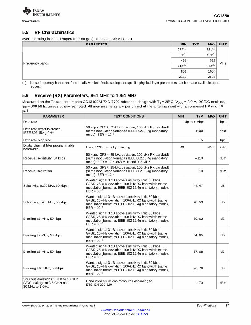
5.5 RF Characteristicsover operating free-air temperature range (unless otherwise noted)
PARAMETER MIN TYP MAX UNIT
Frequency bands
287 (1) 351 (1)
MHz
359 (1) 439 (1)
431 527718 (1) 878 (1)
861 10542152 2635
5.6 Receive (RX) Parameters, 861 MHz to 1054 MHzMeasured on the Texas Instruments CC1310EM-7XD-7793 reference design with Tc = 25°C, VDDS = 3.0 V, DC/DC enabled,fRF = 868 MHz, unless otherwise noted. All measurements are performed at the antenna input with a combined RX and TXpath.
PARAMETER TEST CONDITIONS MIN TYP MAX UNITData rate Up to 4 Mbps bps
Data rate offset tolerance,IEEE 802.15.4g PHY
50 kbps, GFSK, 25-kHz deviation, 100-kHz RX bandwidth(same modulation format as IEEE 802.15.4g mandatorymode), BER = 10–3
1600 ppm
Data rate step size 1.5 bpsDigital channel filter programmablebandwidth Using VCO divide by 5 setting 40 4000 kHz
Receiver sensitivity, 50 kbps50 kbps, GFSK, 25-kHz deviation, 100-kHz RX bandwidth(same modulation format as IEEE 802.15.4g mandatorymode), BER = 10–2. 868 MHz and 915 MHz
–110 dBm
Receiver saturation50 kbps, GFSK, 25-kHz deviation, 100-kHz RX bandwidth(same modulation format as IEEE 802.15.4g mandatorymode), BER = 10–2
10 dBm
Selectivity, ±200 kHz, 50 kbps
Wanted signal 3 dB above sensitivity limit. 50 kbps,GFSK, 25-kHz deviation, 100-kHz RX bandwidth (samemodulation format as IEEE 802.15.4g mandatory mode),BER = 10–2
44, 47 dB
Selectivity, ±400 kHz, 50 kbps
Wanted signal 3 dB above sensitivity limit. 50 kbps,GFSK, 25-kHz deviation, 100-kHz RX bandwidth (samemodulation format as IEEE 802.15.4g mandatory mode),BER = 10–2
48, 53 dB
Blocking ±1 MHz, 50 kbps
Wanted signal 3 dB above sensitivity limit. 50 kbps,GFSK, 25-kHz deviation, 100-kHz RX bandwidth (samemodulation format as IEEE 802.15.4g mandatory mode),BER = 10–2
59, 62 dB
Blocking ±2 MHz, 50 kbps
Wanted signal 3 dB above sensitivity limit. 50 kbps,GFSK, 25-kHz deviation, 100-kHz RX bandwidth (samemodulation format as IEEE 802.15.4g mandatory mode),BER = 10–2
64, 65 dB
Blocking ±5 MHz, 50 kbps
Wanted signal 3 dB above sensitivity limit. 50 kbps,GFSK, 25-kHz deviation, 100-kHz RX bandwidth (samemodulation format as IEEE 802.15.4g mandatory mode),BER = 10–2
67, 68 dB
Blocking ±10 MHz, 50 kbps
Wanted signal 3 dB above sensitivity limit. 50 kbps,GFSK, 25-kHz deviation, 100-kHz RX bandwidth (samemodulation format as IEEE 802.15.4g mandatory mode),BER = 10–2
76, 76 dB
Spurious emissions 1 GHz to 13 GHz(VCO leakage at 3.5 GHz) and30 MHz to 1 GHz
Conducted emissions measured according toETSI EN 300 220 –70 dBm
18
CC1350SWRS183B –JUNE 2016–REVISED JULY 2018 www.ti.com
Submit Documentation FeedbackProduct Folder Links: CC1350
Specifications Copyright © 2016–2018, Texas Instruments Incorporated
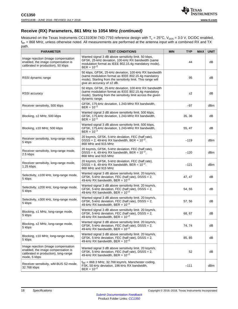
Receive (RX) Parameters, 861 MHz to 1054 MHz (continued)Measured on the Texas Instruments CC1310EM-7XD-7793 reference design with Tc = 25°C, VDDS = 3.0 V, DC/DC enabled,fRF = 868 MHz, unless otherwise noted. All measurements are performed at the antenna input with a combined RX and TXpath.
PARAMETER TEST CONDITIONS MIN TYP MAX UNIT
Image rejection (image compensationenabled, the image compensation iscalibrated in production), 50 kbps
Wanted signal 3 dB above sensitivity limit. 50 kbps,GFSK, 25-kHz deviation, 100-kHz RX bandwidth (samemodulation format as IEEE 802.15.4g mandatory mode),BER = 10–2
44 dB
RSSI dynamic range
50 kbps, GFSK, 25-kHz deviation, 100-kHz RX bandwidth(same modulation format as IEEE 802.15.4g mandatorymode). Starting from the sensitivity limit. This range willgive an accuracy of ±2 dB.
95 dB
RSSI accuracy
50 kbps, GFSK, 25-kHz deviation, 100-kHz RX bandwidth(same modulation format as IEEE 802.15.4g mandatorymode). Starting from the sensitivity limit across the givendynamic range.
±2 dB
Receiver sensitivity, 500 kbps GFSK, 175-kHz deviation, 1.243-MHz RX bandwidth,BER = 10–2 –97 dBm
Blocking, ±2 MHz, 500 kbpsWanted signal 3 dB above sensitivity limit. 500 kbps,GFSK, 175-kHz deviation, 1.243-MHz RX bandwidth,BER = 10–2
35, 36 dB
Blocking, ±10 MHz, 500 kbpsWanted signal 3 dB above sensitivity limit. 500 kbps,GFSK, 175-kHz deviation, 1.243-MHz RX bandwidth,BER = 10–2
55, 47 dB
Receiver sensitivity, long-range mode,5 kbps
20 ksym/s, GFSK, 5-kHz deviation, FEC (half rate),DSSS = 2, 49-kHz RX bandwidth, BER = 10–2.868 MHz and 915 MHz
–119 dBm
Receiver sensitivity, long-range mode,2.5 kbps
20 ksym/s, GFSK, 5-kHz deviation, FEC (half rate),DSSS = 4, 49-kHz RX bandwidth, BER = 10–2.868 MHz and 915 MHz
–120 dBm
Receiver sensitivity, long-range mode,1.25 kbps
20 ksym/s, GFSK, 5-kHz deviation, FEC (half rate),DSSS = 8, 49-kHz RX bandwidth, BER = 10–2.868 MHz and 915 MHz
–121 dBm
Selectivity, ±100 kHz, long-range mode,5 kbps
Wanted signal 3 dB above sensitivity limit. 20 ksym/s,GFSK, 5-kHz deviation, FEC (half rate), DSSS = 2,49-kHz RX bandwidth, BER = 10–2
47, 47 dB
Selectivity, ±200 kHz, long-range mode,5 kbps
Wanted signal 3 dB above sensitivity limit. 20 ksym/s,GFSK, 5-kHz deviation, FEC (half rate), DSSS = 2,49-kHz RX bandwidth, BER = 10–2
54, 55 dB
Selectivity, ±300 kHz, long-range mode,5 kbps
Wanted signal 3 dB above sensitivity limit. 20 ksym/s,GFSK, 5-kHz deviation, FEC (half rate), DSSS = 2,49-kHz RX bandwidth, BER = 10–2
57, 56 dB
Blocking, ±1 MHz, long-range mode,5 kbps
Wanted signal 3 dB above sensitivity limit. 20 ksym/s,GFSK, 5-kHz deviation, FEC (half rate), DSSS = 2,49-kHz RX bandwidth, BER = 10–2
68, 67 dB
Blocking, ±2 MHz, long-range mode,5 kbps
Wanted signal 3 dB above sensitivity limit. 20 ksym/s,GFSK, 5-kHz deviation, FEC (half rate), DSSS = 2,49-kHz RX bandwidth, BER = 10–2
74, 74 dB
Blocking, ±10 MHz, long-range mode,5 kbps
Wanted signal 3 dB above sensitivity limit. 20 ksym/s,GFSK, 5-kHz deviation, FEC (half rate), DSSS = 2,49-kHz RX bandwidth, BER = 10–2
85, 85 dB
Image rejection (image compensationenabled, the image compensation iscalibrated in production), long-rangemode, 5 kbps
Wanted signal 3 dB above sensitivity limit. 20 ksym/s,GFSK, 5-kHz deviation, FEC (half rate), DSSS = 2,49-kHz RX bandwidth, BER = 10–2
52 dB
Receiver sensitivity, wM-BUS S2-mode,32.768 kbps
fRF = 868.3 MHz, 32.768 ksym/s, Manchester coding,FSK, 50-kHz deviation, 196-kHz RX bandwidth,BER = 10–2
–111 dBm
19
CC1350www.ti.com SWRS183B –JUNE 2016–REVISED JULY 2018
Submit Documentation FeedbackProduct Folder Links: CC1350
SpecificationsCopyright © 2016–2018, Texas Instruments Incorporated
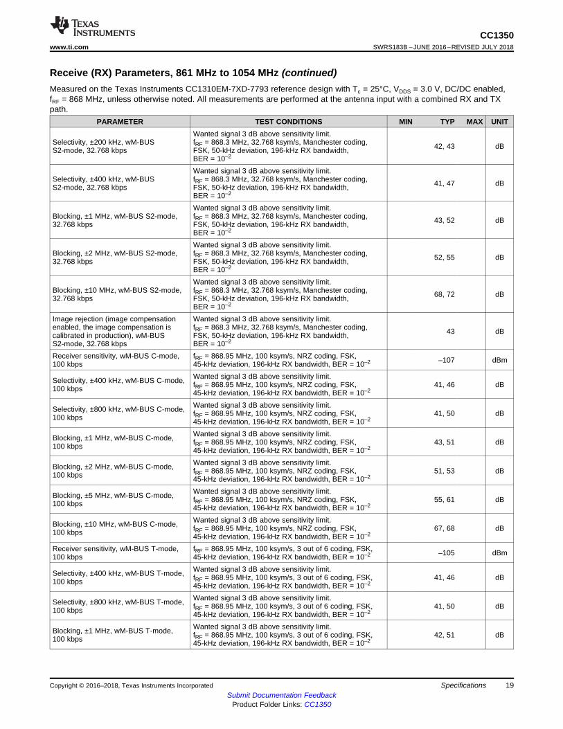
Receive (RX) Parameters, 861 MHz to 1054 MHz (continued)Measured on the Texas Instruments CC1310EM-7XD-7793 reference design with Tc = 25°C, VDDS = 3.0 V, DC/DC enabled,fRF = 868 MHz, unless otherwise noted. All measurements are performed at the antenna input with a combined RX and TXpath.
PARAMETER TEST CONDITIONS MIN TYP MAX UNIT
Selectivity, ±200 kHz, wM-BUSS2-mode, 32.768 kbps
Wanted signal 3 dB above sensitivity limit.fRF = 868.3 MHz, 32.768 ksym/s, Manchester coding,FSK, 50-kHz deviation, 196-kHz RX bandwidth,BER = 10–2
42, 43 dB
Selectivity, ±400 kHz, wM-BUSS2-mode, 32.768 kbps
Wanted signal 3 dB above sensitivity limit.fRF = 868.3 MHz, 32.768 ksym/s, Manchester coding,FSK, 50-kHz deviation, 196-kHz RX bandwidth,BER = 10–2
41, 47 dB
Blocking, ±1 MHz, wM-BUS S2-mode,32.768 kbps
Wanted signal 3 dB above sensitivity limit.fRF = 868.3 MHz, 32.768 ksym/s, Manchester coding,FSK, 50-kHz deviation, 196-kHz RX bandwidth,BER = 10–2
43, 52 dB
Blocking, ±2 MHz, wM-BUS S2-mode,32.768 kbps
Wanted signal 3 dB above sensitivity limit.fRF = 868.3 MHz, 32.768 ksym/s, Manchester coding,FSK, 50-kHz deviation, 196-kHz RX bandwidth,BER = 10–2
52, 55 dB
Blocking, ±10 MHz, wM-BUS S2-mode,32.768 kbps
Wanted signal 3 dB above sensitivity limit.fRF = 868.3 MHz, 32.768 ksym/s, Manchester coding,FSK, 50-kHz deviation, 196-kHz RX bandwidth,BER = 10–2
68, 72 dB
Image rejection (image compensationenabled, the image compensation iscalibrated in production), wM-BUSS2-mode, 32.768 kbps
Wanted signal 3 dB above sensitivity limit.fRF = 868.3 MHz, 32.768 ksym/s, Manchester coding,FSK, 50-kHz deviation, 196-kHz RX bandwidth,BER = 10–2
43 dB
Receiver sensitivity, wM-BUS C-mode,100 kbps
fRF = 868.95 MHz, 100 ksym/s, NRZ coding, FSK,45-kHz deviation, 196-kHz RX bandwidth, BER = 10–2 –107 dBm
Selectivity, ±400 kHz, wM-BUS C-mode,100 kbps
Wanted signal 3 dB above sensitivity limit.fRF = 868.95 MHz, 100 ksym/s, NRZ coding, FSK,45-kHz deviation, 196-kHz RX bandwidth, BER = 10–2
41, 46 dB
Selectivity, ±800 kHz, wM-BUS C-mode,100 kbps
Wanted signal 3 dB above sensitivity limit.fRF = 868.95 MHz, 100 ksym/s, NRZ coding, FSK,45-kHz deviation, 196-kHz RX bandwidth, BER = 10–2
41, 50 dB
Blocking, ±1 MHz, wM-BUS C-mode,100 kbps
Wanted signal 3 dB above sensitivity limit.fRF = 868.95 MHz, 100 ksym/s, NRZ coding, FSK,45-kHz deviation, 196-kHz RX bandwidth, BER = 10–2
43, 51 dB
Blocking, ±2 MHz, wM-BUS C-mode,100 kbps
Wanted signal 3 dB above sensitivity limit.fRF = 868.95 MHz, 100 ksym/s, NRZ coding, FSK,45-kHz deviation, 196-kHz RX bandwidth, BER = 10–2
51, 53 dB
Blocking, ±5 MHz, wM-BUS C-mode,100 kbps
Wanted signal 3 dB above sensitivity limit.fRF = 868.95 MHz, 100 ksym/s, NRZ coding, FSK,45-kHz deviation, 196-kHz RX bandwidth, BER = 10–2
55, 61 dB
Blocking, ±10 MHz, wM-BUS C-mode,100 kbps
Wanted signal 3 dB above sensitivity limit.fRF = 868.95 MHz, 100 ksym/s, NRZ coding, FSK,45-kHz deviation, 196-kHz RX bandwidth, BER = 10–2
67, 68 dB
Receiver sensitivity, wM-BUS T-mode,100 kbps
fRF = 868.95 MHz, 100 ksym/s, 3 out of 6 coding, FSK,45-kHz deviation, 196-kHz RX bandwidth, BER = 10–2 –105 dBm
Selectivity, ±400 kHz, wM-BUS T-mode,100 kbps
Wanted signal 3 dB above sensitivity limit.fRF = 868.95 MHz, 100 ksym/s, 3 out of 6 coding, FSK,45-kHz deviation, 196-kHz RX bandwidth, BER = 10–2
41, 46 dB
Selectivity, ±800 kHz, wM-BUS T-mode,100 kbps
Wanted signal 3 dB above sensitivity limit.fRF = 868.95 MHz, 100 ksym/s, 3 out of 6 coding, FSK,45-kHz deviation, 196-kHz RX bandwidth, BER = 10–2
41, 50 dB
Blocking, ±1 MHz, wM-BUS T-mode,100 kbps
Wanted signal 3 dB above sensitivity limit.fRF = 868.95 MHz, 100 ksym/s, 3 out of 6 coding, FSK,45-kHz deviation, 196-kHz RX bandwidth, BER = 10–2
42, 51 dB

20
CC1350SWRS183B –JUNE 2016–REVISED JULY 2018 www.ti.com
Submit Documentation FeedbackProduct Folder Links: CC1350
Specifications Copyright © 2016–2018, Texas Instruments Incorporated
Receive (RX) Parameters, 861 MHz to 1054 MHz (continued)Measured on the Texas Instruments CC1310EM-7XD-7793 reference design with Tc = 25°C, VDDS = 3.0 V, DC/DC enabled,fRF = 868 MHz, unless otherwise noted. All measurements are performed at the antenna input with a combined RX and TXpath.
PARAMETER TEST CONDITIONS MIN TYP MAX UNIT
Blocking, ±2 MHz, wM-BUS T-mode,100 kbps
Wanted signal 3 dB above sensitivity limit.fRF = 868.95 MHz, 100 ksym/s, 3 out of 6 coding, FSK,45-kHz deviation, 196-kHz RX bandwidth, BER = 10–2
51, 52 dB
Blocking, ±5 MHz, wM-BUS T-mode,100 kbps
Wanted signal 3 dB above sensitivity limit.fRF = 868.95 MHz, 100 ksym/s, 3 out of 6 coding, FSK,45-kHz deviation, 196-kHz RX bandwidth, BER = 10–2
54, 60 dB
Blocking, ±10 MHz, wM-BUS T-mode,100 kbps
Wanted signal 3 dB above sensitivity limit.fRF = 868.95 MHz, 100 ksym/s, 3 out of 6 coding, FSK,45-kHz deviation, 196-kHz RX bandwidth, BER = 10–2
67, 68 dB
Receiver sensitivity, WideBand-DSSS(WB-DSSS), 30 kbps
fRF = 915 MHz, 480 ksym/s, GFSK, 195-kHz deviation,FEC (half rate), DSSS = 8, 622-kHz RX bandwidth,BER = 10–2
–109 dBm
Blocking, ±1 MHz, WB-DSSS, 30 kbps
Wanted signal 3 dB above sensitivity limit.fRF = 915 MHz, 480 ksym/s, GFSK, 195-kHz deviation,FEC (half rate), DSSS = 8, 622-kHz RX bandwidth,BER = 10–2
57, 57 dB
Blocking, ±2 MHz, WB-DSSS, 30 kbps
Wanted signal 3 dB above sensitivity limit.fRF = 915 MHz, 480 ksym/s, GFSK, 195-kHz deviation,FEC (half rate), DSSS = 8, 622-kHz RX bandwidth,BER = 10–2
58, 58 dB
Blocking, ±5 MHz, WB-DSSS, 30 kbps
Wanted signal 3 dB above sensitivity limit.fRF = 915 MHz, 480 ksym/s, GFSK, 195-kHz deviation,FEC (half rate), DSSS = 8, 622-kHz RX bandwidth,BER = 10–2
59, 57 dB
Blocking, ±10 MHz, WB-DSSS, 30 kbps
Wanted signal 3 dB above sensitivity limit.fRF = 915 MHz, 480 ksym/s, GFSK, 195-kHz deviation,FEC (half rate), DSSS = 8, 622-kHz RX bandwidth,BER = 10–2
71, 68 dB
Receiver sensitivity, WideBand-DSSS(WB-DSSS), 60 kbps
fRF = 915 MHz, 480 ksym/s, GFSK, 195-kHz deviation,FEC (half rate), DSSS = 4, 622-kHz RX bandwidth,BER = 10–2
–108 dBm
Blocking, ±1 MHz, WB-DSSS, 60 kbps
Wanted signal 3 dB above sensitivity limit.fRF = 915 MHz, 480 ksym/s, GFSK, 195-kHz deviation,FEC (half rate), DSSS = 4, 622-kHz RX bandwidth,BER = 10–2
56, 56 dB
Blocking, ±2 MHz, WB-DSSS, 60 kbps
Wanted signal 3 dB above sensitivity limit.fRF = 915 MHz, 480 ksym/s, GFSK, 195-kHz deviation,FEC (half rate), DSSS = 4, 622-kHz RX bandwidth,BER = 10–2
57, 57 dB
Blocking, ±5 MHz, WB-DSSS, 60 kbps
Wanted signal 3 dB above sensitivity limit.fRF = 915 MHz, 480 ksym/s, GFSK, 195-kHz deviation,FEC (half rate), DSSS = 4, 622-kHz RX bandwidth,BER = 10–2
57, 56 dB
Blocking, ±10 MHz, WB-DSSS, 60 kbps
Wanted signal 3 dB above sensitivity limit.fRF = 915 MHz, 480 ksym/s, GFSK, 195-kHz deviation,FEC (half rate), DSSS = 4, 622-kHz RX bandwidth,BER = 10–2
70, 67 dB
Receiver sensitivity, WideBand-DSSS(WB-DSSS), 120 kbps
fRF = 915 MHz, 480 ksym/s, GFSK, 195-kHz deviation,FEC (half rate), DSSS = 2, 622-kHz RX bandwidth,BER = 10–2
–106 dBm
Blocking, ±1 MHz, WB-DSSS, 120 kbps
Wanted signal 3 dB above sensitivity limit.fRF = 915 MHz, 480 ksym/s, GFSK, 195-kHz deviation,FEC (half rate), DSSS = 2, 622-kHz RX bandwidth,BER = 10–2
54, 54 dB
Blocking, ±2 MHz, WB-DSSS, 120 kbps
Wanted signal 3 dB above sensitivity limit.fRF = 915 MHz, 480 ksym/s, GFSK, 195-kHz deviation,FEC (half rate), DSSS = 2, 622-kHz RX bandwidth,BER = 10–2
55, 55 dB
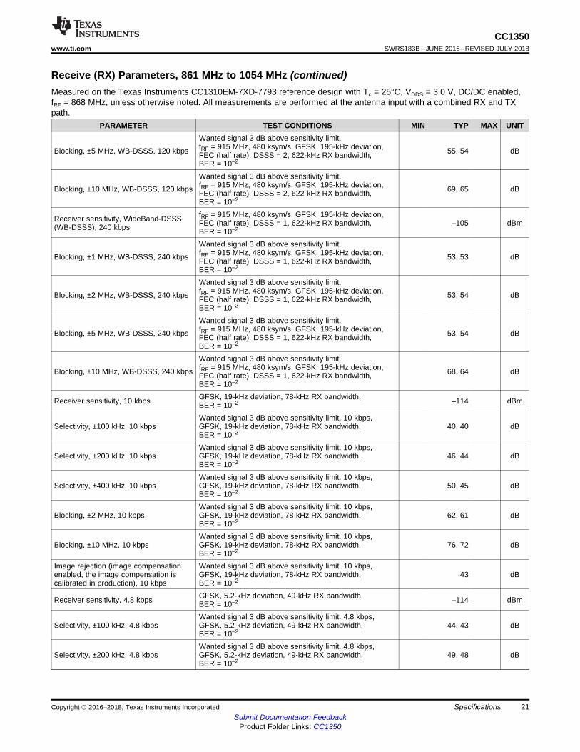
21
CC1350www.ti.com SWRS183B –JUNE 2016–REVISED JULY 2018
Submit Documentation FeedbackProduct Folder Links: CC1350
SpecificationsCopyright © 2016–2018, Texas Instruments Incorporated
Receive (RX) Parameters, 861 MHz to 1054 MHz (continued)Measured on the Texas Instruments CC1310EM-7XD-7793 reference design with Tc = 25°C, VDDS = 3.0 V, DC/DC enabled,fRF = 868 MHz, unless otherwise noted. All measurements are performed at the antenna input with a combined RX and TXpath.
PARAMETER TEST CONDITIONS MIN TYP MAX UNIT
Blocking, ±5 MHz, WB-DSSS, 120 kbps
Wanted signal 3 dB above sensitivity limit.fRF = 915 MHz, 480 ksym/s, GFSK, 195-kHz deviation,FEC (half rate), DSSS = 2, 622-kHz RX bandwidth,BER = 10–2
55, 54 dB
Blocking, ±10 MHz, WB-DSSS, 120 kbps
Wanted signal 3 dB above sensitivity limit.fRF = 915 MHz, 480 ksym/s, GFSK, 195-kHz deviation,FEC (half rate), DSSS = 2, 622-kHz RX bandwidth,BER = 10–2
69, 65 dB
Receiver sensitivity, WideBand-DSSS(WB-DSSS), 240 kbps
fRF = 915 MHz, 480 ksym/s, GFSK, 195-kHz deviation,FEC (half rate), DSSS = 1, 622-kHz RX bandwidth,BER = 10–2
–105 dBm
Blocking, ±1 MHz, WB-DSSS, 240 kbps
Wanted signal 3 dB above sensitivity limit.fRF = 915 MHz, 480 ksym/s, GFSK, 195-kHz deviation,FEC (half rate), DSSS = 1, 622-kHz RX bandwidth,BER = 10–2
53, 53 dB
Blocking, ±2 MHz, WB-DSSS, 240 kbps
Wanted signal 3 dB above sensitivity limit.fRF = 915 MHz, 480 ksym/s, GFSK, 195-kHz deviation,FEC (half rate), DSSS = 1, 622-kHz RX bandwidth,BER = 10–2
53, 54 dB
Blocking, ±5 MHz, WB-DSSS, 240 kbps
Wanted signal 3 dB above sensitivity limit.fRF = 915 MHz, 480 ksym/s, GFSK, 195-kHz deviation,FEC (half rate), DSSS = 1, 622-kHz RX bandwidth,BER = 10–2
53, 54 dB
Blocking, ±10 MHz, WB-DSSS, 240 kbps
Wanted signal 3 dB above sensitivity limit.fRF = 915 MHz, 480 ksym/s, GFSK, 195-kHz deviation,FEC (half rate), DSSS = 1, 622-kHz RX bandwidth,BER = 10–2
68, 64 dB
Receiver sensitivity, 10 kbps GFSK, 19-kHz deviation, 78-kHz RX bandwidth,BER = 10–2 –114 dBm
Selectivity, ±100 kHz, 10 kbpsWanted signal 3 dB above sensitivity limit. 10 kbps,GFSK, 19-kHz deviation, 78-kHz RX bandwidth,BER = 10–2
40, 40 dB
Selectivity, ±200 kHz, 10 kbpsWanted signal 3 dB above sensitivity limit. 10 kbps,GFSK, 19-kHz deviation, 78-kHz RX bandwidth,BER = 10–2
46, 44 dB
Selectivity, ±400 kHz, 10 kbpsWanted signal 3 dB above sensitivity limit. 10 kbps,GFSK, 19-kHz deviation, 78-kHz RX bandwidth,BER = 10–2
50, 45 dB
Blocking, ±2 MHz, 10 kbpsWanted signal 3 dB above sensitivity limit. 10 kbps,GFSK, 19-kHz deviation, 78-kHz RX bandwidth,BER = 10–2
62, 61 dB
Blocking, ±10 MHz, 10 kbpsWanted signal 3 dB above sensitivity limit. 10 kbps,GFSK, 19-kHz deviation, 78-kHz RX bandwidth,BER = 10–2
76, 72 dB
Image rejection (image compensationenabled, the image compensation iscalibrated in production), 10 kbps
Wanted signal 3 dB above sensitivity limit. 10 kbps,GFSK, 19-kHz deviation, 78-kHz RX bandwidth,BER = 10–2
43 dB
Receiver sensitivity, 4.8 kbps GFSK, 5.2-kHz deviation, 49-kHz RX bandwidth,BER = 10–2 –114 dBm
Selectivity, ±100 kHz, 4.8 kbpsWanted signal 3 dB above sensitivity limit. 4.8 kbps,GFSK, 5.2-kHz deviation, 49-kHz RX bandwidth,BER = 10–2
44, 43 dB
Selectivity, ±200 kHz, 4.8 kbpsWanted signal 3 dB above sensitivity limit. 4.8 kbps,GFSK, 5.2-kHz deviation, 49-kHz RX bandwidth,BER = 10–2
49, 48 dB

22
CC1350SWRS183B –JUNE 2016–REVISED JULY 2018 www.ti.com
Submit Documentation FeedbackProduct Folder Links: CC1350
Specifications Copyright © 2016–2018, Texas Instruments Incorporated
Receive (RX) Parameters, 861 MHz to 1054 MHz (continued)Measured on the Texas Instruments CC1310EM-7XD-7793 reference design with Tc = 25°C, VDDS = 3.0 V, DC/DC enabled,fRF = 868 MHz, unless otherwise noted. All measurements are performed at the antenna input with a combined RX and TXpath.
PARAMETER TEST CONDITIONS MIN TYP MAX UNIT
Selectivity, ±400 kHz, 4.8 kbpsWanted signal 3 dB above sensitivity limit. 4.8 kbps,GFSK, 5.2-kHz deviation, 49-kHz RX bandwidth,BER = 10–2
52, 49 dB
Blocking, ±2 MHz, 4.8 kbpsWanted signal 3 dB above sensitivity limit. 4.8 kbps,GFSK, 5.2-kHz deviation, 49-kHz RX bandwidth,BER = 10–2
64, 63 dB
Blocking, ±10 MHz, 4.8 kbpsWanted signal 3 dB above sensitivity limit. 4.8 kbps,GFSK, 5.2-kHz deviation, 49-kHz RX bandwidth,BER = 10–2
73, 72 dB
Image rejection (image compensationenabled, the image compensation iscalibrated in production), 4.8 kbps
Wanted signal 3 dB above sensitivity limit. 4.8 kbps,GFSK, 5.2-kHz deviation, 49-kHz RX bandwidth,BER = 10–2
43 dB
Receiver sensitivity, CC1101 compatiblemode, 2.4 kbps
GFSK, 5.2-kHz deviation (commonly used settings onCC1101), 49-kHz RX bandwidth, BER = 10–2 –116 dBm
Selectivity, ±100 kHz, CC1101compatible mode, 2.4 kbps
Wanted signal 3 dB above sensitivity limit. 2.4 kbps,GFSK, 5.2-kHz deviation (commonly used settings onCC1101), 49-kHz RX bandwidth, BER = 10–2
45, 44 dB
Selectivity, ±200 kHz, CC1101compatible mode, 2.4 kbps
Wanted signal 3 dB above sensitivity limit. 2.4 kbps,GFSK, 5.2-kHz deviation (commonly used settings onCC1101), 49-kHz RX bandwidth, BER = 10–2
51, 47 dB
Blocking, ±2 MHz, CC1101 compatiblemode, 2.4 kbps
Wanted signal 3 dB above sensitivity limit. 2.4 kbps,GFSK, 5.2-kHz deviation (commonly used settings onCC1101), 49-kHz RX bandwidth, BER = 10–2
63, 62 dB
Blocking, ±10 MHz, CC1101 compatiblemode, 2.4 kbps
Wanted signal 3 dB above sensitivity limit. 2.4 kbps,GFSK, 5.2-kHz deviation (commonly used settings onCC1101), 49-kHz RX bandwidth, BER = 10–2
76, 71 dB
Image rejection (image compensationenabled, the image compensation iscalibrated in production), CC1101compatible mode, 2.4 kbps
Wanted signal 3 dB above sensitivity limit. 2.4 kbps,GFSK, 5.2-kHz deviation (commonly used settings onCC1101), 49-kHz RX bandwidth, BER = 10–2
45 dB
Receiver sensitivity, CC1101 compatiblemode, 1.2 kbps
GFSK, 5.2-kHz deviation (commonly used settings onCC1101), 49-kHz RX bandwidth, BER = 10–2 –117 dBm
Selectivity, ±100 kHz, CC1101compatible mode, 1.2 kbps
Wanted signal 3 dB above sensitivity limit. 1.2 kbps,GFSK, 5.2-kHz deviation (commonly used settings onCC1101), 49-kHz RX bandwidth, BER = 10–2
45, 44 dB
Selectivity, ±200 kHz, CC1101compatible mode, 1.2 kbps
Wanted signal 3 dB above sensitivity limit. 1.2 kbps,GFSK, 5.2-kHz deviation (commonly used settings onCC1101), 49-kHz RX bandwidth, BER = 10–2
51, 47 dB
Blocking, ±2 MHz, CC1101 compatiblemode, 1.2 kbps
Wanted signal 3 dB above sensitivity limit. 1.2 kbps,GFSK, 5.2-kHz deviation (commonly used settings onCC1101), 49-kHz RX bandwidth, BER = 10–2
63, 62 dB
Blocking, ±10 MHz, CC1101 compatiblemode, 1.2 kbps
Wanted signal 3 dB above sensitivity limit. 1.2 kbps,GFSK, 5.2-kHz deviation (commonly used settings onCC1101), 49-kHz RX bandwidth, BER = 10–2
81, 81 dB
Image rejection (image compensationenabled, the image compensation iscalibrated in production), CC1101compatible mode, 1.2 kbps
Wanted signal 3 dB above sensitivity limit. 1.2 kbps,GFSK, 5.2-kHz deviation (commonly used settings onCC1101), 49-kHz RX bandwidth, BER = 10–2
45 dB
Receiver sensitivity, legacy long-rangemode, 625 bps
10 ksym/s, GFSK, 5-kHz deviation, FEC (half rate),DSSS = 8, 40-kHz RX bandwidth, BER = 10–2.868 MHz and 915 MHz.
–124 dBm
Selectivity, ±100 kHz, legacy long-rangemode, 625 bps
Wanted signal 3 dB above sensitivity limit. 10 ksym/s,GFSK, 5-kHz deviation, FEC (half rate), DSSS = 8,40-kHz RX bandwidth, BER = 10–2
56, 56 dB
Blocking ±1 MHz, legacy long-rangemode, 625 bps
Wanted signal 3 dB above sensitivity limit. 10 ksym/s,GFSK, 5-kHz deviation, FEC (half rate), DSSS = 8,40-kHz RX bandwidth, BER = 10–2
73, 77 dB
23
CC1350www.ti.com SWRS183B –JUNE 2016–REVISED JULY 2018
Submit Documentation FeedbackProduct Folder Links: CC1350
SpecificationsCopyright © 2016–2018, Texas Instruments Incorporated
Receive (RX) Parameters, 861 MHz to 1054 MHz (continued)Measured on the Texas Instruments CC1310EM-7XD-7793 reference design with Tc = 25°C, VDDS = 3.0 V, DC/DC enabled,fRF = 868 MHz, unless otherwise noted. All measurements are performed at the antenna input with a combined RX and TXpath.
PARAMETER TEST CONDITIONS MIN TYP MAX UNIT
Blocking ±2 MHz, legacy long-rangemode, 625 bps
Wanted signal 3 dB above sensitivity limit. 10 ksym/s,GFSK, 5-kHz deviation, FEC (half rate), DSSS = 8,40-kHz RX bandwidth, BER = 10–2
79, 79 dB
Blocking ±10 MHz, legacy long-rangemode, 625 bps
Wanted signal 3 dB above sensitivity limit. 10 ksym/s,GFSK, 5-kHz deviation, FEC (half rate), DSSS = 8,40-kHz RX bandwidth, BER = 10–2
91, 91 dB
Receiver sensitivity, OOK, 4.8 kbps 4.8 kbps, OOK, 40-kHz RX bandwidth, BER = 10–2.868 MHz and 915 MHz –115 dBm
5.7 Receive (RX) Parameters, 431 MHz to 527 MHzMeasured on the Texas Instruments CC1310EM-7XD-4251 reference design with Tc = 25°C, VDDS = 3.0 V, DC/DC enabled,fRF = 433.92 MHz, unless otherwise noted. All measurements are performed at the antenna input with a combined RX and TXpath.
PARAMETER TEST CONDITIONS MIN TYP MAX UNIT
Receiver sensitivity, 50 kbps50 kbps, GFSK, 25-kHz deviation, 100-kHz RX bandwidth(same modulation format as IEEE 802.15.4g mandatorymode), BER = 10–2
–110 dBm
Receiver saturation50 kbps, GFSK, 25-kHz deviation, 100-kHz RX bandwidth(same modulation format as IEEE 802.15.4g mandatorymode), BER = 10–2
10 dBm
Selectivity, ±200 kHz, 50 kbps
Wanted signal 3 dB above sensitivity limit. 50 kbps,GFSK, 25-kHz deviation, 100-kHz RX bandwidth (samemodulation format as IEEE 802.15.4g mandatory mode),BER = 10–2
40, 42 dB
Selectivity, ±400 kHz, 50 kbps
Wanted signal 3 dB above sensitivity limit. 50 kbps,GFSK, 25-kHz deviation, 100-kHz RX bandwidth (samemodulation format as IEEE 802.15.4g mandatory mode),BER = 10–2
42, 50 dB
Blocking ±1 MHz, 50 kbps
Wanted signal 3 dB above sensitivity limit. 50 kbps,GFSK, 25-kHz deviation, 100-kHz RX bandwidth (samemodulation format as IEEE 802.15.4g mandatory mode),BER = 10–2
53, 58 dB
Blocking ±2 MHz, 50 kbps
Wanted signal 3 dB above sensitivity limit. 50 kbps,GFSK, 25-kHz deviation, 100-kHz RX bandwidth (samemodulation format as IEEE 802.15.4g mandatory mode),BER = 10–2
59, 60 dB
Blocking ±10 MHz, 50 kbps
Wanted signal 3 dB above sensitivity limit. 50 kbps,GFSK, 25-kHz deviation, 100-kHz RX bandwidth (samemodulation format as IEEE 802.15.4g mandatory mode),BER = 10–2
74, 74 dB
Spurious emissions 1 GHz to 13 GHz(VCO leakage at 3.5 GHz) and30 MHz to 1 GHz
Conducted emissions measured according toETSI EN 300 220 –74 dBm
Image rejection (image compensationenabled, the image compensation iscalibrated in production), 50 kbps
Wanted signal 3 dB above sensitivity limit. 50 kbps,GFSK, 25-kHz deviation, 100-kHz RX bandwidth (samemodulation format as IEEE 802.15.4g mandatory mode),BER = 10–2
43 dB
Receiver sensitivity, long-range mode,5 kbps
20 ksym/s, GFSK, 5-kHz deviation, FEC (half rate),DSSS = 2, 49-kHz RX bandwidth, BER = 10–2. 433 MHz –119 dBm
Receiver sensitivity, long-range mode,2.5 kbps
20 ksym/s, GFSK, 5-kHz deviation, FEC (half rate),DSSS = 4, 49-kHz RX bandwidth, BER = 10–2. 433 MHz –120 dBm
Receiver sensitivity, long-range mode,1.25 kbps
20 ksym/s, GFSK, 5-kHz deviation, FEC (half rate),DSSS = 8, 49-kHz RX bandwidth, BER = 10–2. 433 MHz –121 dBm

24
CC1350SWRS183B –JUNE 2016–REVISED JULY 2018 www.ti.com
Submit Documentation FeedbackProduct Folder Links: CC1350
Specifications Copyright © 2016–2018, Texas Instruments Incorporated
Receive (RX) Parameters, 431 MHz to 527 MHz (continued)Measured on the Texas Instruments CC1310EM-7XD-4251 reference design with Tc = 25°C, VDDS = 3.0 V, DC/DC enabled,fRF = 433.92 MHz, unless otherwise noted. All measurements are performed at the antenna input with a combined RX and TXpath.
PARAMETER TEST CONDITIONS MIN TYP MAX UNIT
Receiver sensitivity, legacy long-rangemode, 625 bps
10 ksym/s, GFSK, 5-kHz deviation, FEC (half rate),DSSS = 8, 40-kHz RX bandwidth, BER = 10–2.868 MHz and 915 MHZ.
–124 dBm
Selectivity, ±100 kHz, legacy long-rangemode, 625 bps
Wanted signal 3 dB above sensitivity limit. 10 ksym/s,GFSK, 5-kHz deviation, FEC (half rate), DSSS = 8,40-kHz RX bandwidth, BER = 10–2
56, 56 dB
Selectivity, ±200 kHz, legacy long-rangemode, 625 bps
Wanted signal 3 dB above sensitivity limit. 10 ksym/s,GFSK, 5-kHz deviation, FEC (half rate), DSSS = 8,40-kHz RX bandwidth, BER = 10–2
62, 65 dB
Blocking ±1 MHz, legacy long-rangemode, 625 bps
Wanted signal 3 dB above sensitivity limit. 10 ksym/s,GFSK, 5-kHz deviation, FEC (half rate), DSSS = 8,40-kHz RX bandwidth, BER = 10–2
68, 73 dB
Blocking ±2 MHz, legacy long-rangemode, 625 bps
Wanted signal 3 dB above sensitivity limit. 10 ksym/s,GFSK, 5-kHz deviation, FEC (half rate), DSSS = 8,40-kHz RX bandwidth, BER = 10–2
74, 74 dB
Blocking ±10 MHz, legacy long-rangemode, 625 bps
Wanted signal 3 dB above sensitivity limit. 10 ksym/s,GFSK, 5-kHz deviation, FEC (half rate), DSSS = 8,40-kHz RX bandwidth, BER = 10–2
88, 89 dB
Image rejection (image compensationenabled, the image compensation iscalibrated in production), legacy long-range mode, 625 bps
Wanted signal 3 dB above sensitivity limit. 10 ksym/s,GFSK, 5-kHz deviation, FEC (half rate), DSSS = 8,40-kHz RX bandwidth, BER = 10–2
55 dB

25
CC1350www.ti.com SWRS183B –JUNE 2016–REVISED JULY 2018
Submit Documentation FeedbackProduct Folder Links: CC1350
SpecificationsCopyright © 2016–2018, Texas Instruments Incorporated
(1) Suitable for systems targeting compliance with EN 300 220, EN 54-25, EN 303 204, FCC CFR47 Part 15, ARIB STD-T108.
5.8 Transmit (TX) Parameters, 861 MHz to 1054 MHzMeasured on the Texas Instruments CC1310EM-7XD-7793 reference design with Tc = 25°C, VDDS = 3.0 V, DC/DC enabled,fRF = 868 MHz, unless otherwise noted. All measurements are performed at the antenna input with a combined RX and TXpath.
PARAMETER TEST CONDITIONS MIN TYP MAX UNIT
Maximum output power, boost modeVDDR = 1.95 VMinimum VDDS for boost mode is 2.1 V868 MHz and 915 MHz
14 dBm
Maximum output power 868 MHz and 915 MHz 12 dBmOutput power programmable range 24 dBOutput power variation Tested at +10-dBm setting ±0.9 dBOutput power variation, boost mode +14 dBm ±0.5 dB
Spurious emissions(excluding harmonics) (1)
30 MHz to 1 GHz
Transmitting +14 dBmETSI restricted bands <–59
dBmTransmitting +14 dBmoutside ETSI restricted bands <–51
1 GHz to 12.75 GHz Transmitting +14 dBmmeasured in 1-MHz bandwidth (ETSI) <–37
Harmonics
Second harmonic Transmitting +14 dBm, conducted868 MHz, 915 MHz –52, –55
dBmThird harmonic Transmitting +14 dBm, conducted868 MHz, 915 MHz –58, –55
Fourth harmonic Transmitting +14 dBm, conducted868 MHz, 915 MHz –56, –56
Spurious emissionsout-of-band,915 MHz (1)
30 MHz to 88 MHz(within FCC restricted bands) Transmitting +14 dBm, conducted <–66
dBm
88 MHz to 216 MHz(within FCC restricted bands) Transmitting +14 dBm, conducted <–65
216 MHz to 960 MHz(within FCC restricted bands) Transmitting +14 dBm, conducted <–65
960 MHz to 2390 MHz andabove 2483.5 MHz (withinFCC restricted band)
Transmitting +14 dBm, conducted <–52
1 GHz to 12.75 GHz(outside FCC restrictedbands)
Transmitting +14 dBm, conducted <–43
Spurious emissionsout-of-band,920.6 MHz (1)
Below 710 MHz(ARIB T-108) Transmitting +14 dBm, conducted <–50
dBm
710 MHz to 900 MHz(ARIB T-108) Transmitting +14 dBm, conducted <–60
900 MHz to 915 MHz(ARIB T-108) Transmitting +14 dBm, conducted <–57
930 MHz to 1000 MHz(ARIB T-108) Transmitting +14 dBm, conducted <–57
1000 MHz to 1215 MHz(ARIB T-108) Transmitting +14 dBm, conducted <–59
Above 1215 MHz(ARIB T-108) Transmitting +14 dBm, conducted <–45
26
CC1350SWRS183B –JUNE 2016–REVISED JULY 2018 www.ti.com
Submit Documentation FeedbackProduct Folder Links: CC1350
Specifications Copyright © 2016–2018, Texas Instruments Incorporated
(1) Suitable for systems targeting compliance with EN 300 220, EN 54-25, EN 303 204, FCC CFR47 Part 15, ARIB STD-T108.
5.9 Transmit (TX) Parameters, 431 MHz to 527 MHzMeasured on the Texas Instruments CC1310EM-7XD-4251 reference design with Tc = 25°C, VDDS = 3.0 V, DC/DC enabled,fRF = 433.92 MHz, unless otherwise noted. All measurements are performed at the antenna input with a combined RX and TXpath.
PARAMETER TEST CONDITIONS MIN TYP MAX UNIT
Maximum output power, boost mode VDDR = 1.95 VMinimum VDDS for boost mode is 2.1 V 15 dBm
Maximum output power 14 dBm
Spurious emissions(excluding harmonics) (1)
30 MHz to 1 GHz
Transmitting +10 dBm, 433 MHzInside ETSI restricted bands <–63
dBm
Transmitting +10 dBm, 433 MHzOutside ETSI restricted bands <–39
1 GHz to 12.75 GHz
Transmitting +10 dBm, 433 MHzOutside ETSI restricted bands, measuredin 1-MHz bandwidth (ETSI)
<–52
Transmitting +10 dBm, 433 MHzInside ETSI restricted bands, measured in1-MHz bandwidth (ETSI)
<–58
(1) Numbers given as I/C dB.(2) X / Y, where X is +N MHz and Y is –N MHz.
5.10 1-Mbps GFSK (Bluetooth low energy) – RXMeasured on the TI CC1350_7XD-Dual Band reference design with Tc = 25°C, VDDS = 3.0 V, fRF = 2440 MHz, unlessotherwise noted. All tests with Bluetooth low energy PHY (1 Mbps), 37-byte payload unless otherwise noted.
PARAMETER TEST CONDITIONS MIN TYP MAX UNIT
Receiver sensitivityDifferential mode. Measured at the CC1350_7XD-Dual Band SMA connector,37-byte payload BER = 10–3
–87 dBm
Receiver sensitivityDifferential mode. Measured at the CC1350_7XD-Dual Band SMA connector,255-byte payload BER = 10–3
–86 dBm
Receiver saturation Differential mode. Measured at the CC1350_7XD-Dual Band SMA connector, BER = 10–3 0 dBm
Frequency error toleranceDifference between the incoming carrier frequencyand the internally generated carrier frequency.Input signal 10 dB above sensitivity limit
–350 350 kHz
Data rate error toleranceDifference between incoming data rate and theinternally generated data rate. Input signal 10 dBabove sensitivity limit
–750 750 ppm
Co-channel rejection (1) Wanted signal at –67 dBm, modulated interferer inchannel, BER = 10–3 –6 dB
Selectivity, ±1 MHz (1) Wanted signal at –67 dBm, modulated interferer at±1 MHz, BER = 10–3 7 / 4 (2) dB
Selectivity, +2 MHz (1) Wanted signal at –67 dBm, modulated interferer at+2 MHz, BER = 10–3 38 dB
Selectivity, ±3 MHz (1)
Wanted signal at –67 dBm, modulated interferer at±3 MHz, BER = 10–3.Note that –3 MHz is –1 MHz from the imagefrequency.
36 / 41 (2) dB
Selectivity, ±4 MHz (1) Wanted signal at –67 dBm, modulated interferer at±4 MHz, BER = 10–3 39 / 38 (2) dB
Selectivity, ±5 MHz (1) Wanted signal at –67 dBm, modulated interferer at±5 MHz, BER = 10–3 35 / 39 (2) dB
Selectivity, ±6 MHz (1) Wanted signal at –67 dBm, modulated interferer at≥ ±6 MHz, BER = 10–3 42 / 37 (2) dB
Selectivity, ±15 MHz or more (1) Wanted signal at –67 dBm, modulated interferer at≥ ±15 MHz or more, BER = 10–3 55 dB

27
CC1350www.ti.com SWRS183B –JUNE 2016–REVISED JULY 2018
Submit Documentation FeedbackProduct Folder Links: CC1350
SpecificationsCopyright © 2016–2018, Texas Instruments Incorporated
1-Mbps GFSK (Bluetooth low energy) – RX (continued)Measured on the TI CC1350_7XD-Dual Band reference design with Tc = 25°C, VDDS = 3.0 V, fRF = 2440 MHz, unlessotherwise noted. All tests with Bluetooth low energy PHY (1 Mbps), 37-byte payload unless otherwise noted.
PARAMETER TEST CONDITIONS MIN TYP MAX UNIT
(3) Excluding one exception at Fwanted / 2, per Bluetooth Specification.
Selectivity, Image frequency(image compensation enabled,the image compensation iscalibrated in production) (1)
Wanted signal at –67 dBm, modulated interferer atimage frequency, BER = 10–3 37 dB
Selectivity, Image frequency±1 MHz (1)
Wanted signal at –67 dBm, modulated interferer at±1 MHz from image (–3 MHz and –1 MHz fromwanted) frequency, BER = 10–3
4 / 41 (2) dB
Out-of-band blocking (3) 30 MHz to 2000 MHz –25 dBmOut-of-band blocking 2003 MHz to 2399 MHz >–20 dBmOut-of-band blocking 2484 MHz to 2997 MHz >–20 dBmOut-of-band blocking 3000 MHz to 12.75 GHz >–30 dBm
IntermodulationWanted signal at 2402 MHz, –64 dBm. Twointerferers at 2405 and 2408 MHz, respectively, atthe given power level
–30 dBm
Spurious emissions,30 to 1000 MHz
Conducted measurement in a 50-Ω single-endedload. Suitable for systems targeting compliancewith EN 300 328, EN 300 440 class 2, FCCCFR47, Part 15 and ARIB STD-T-66
–72 dBm
Spurious emissions,1 to 12.75 GHz
Conducted measurement in a 50-Ω single-endedload. Suitable for systems targeting compliancewith EN 300 328, EN 300 440 class 2, FCCCFR47, Part 15 and ARIB STD-T-66
–65 dBm
RSSI dynamic range 70 dBRSSI accuracy ±4 dB
(1) Suitable for systems targeting compliance with worldwide radio-frequency regulations ETSI EN 300 328 and EN 300 440 Class 2(Europe), FCC CFR47 Part 15 (US), and ARIB STD-T66 (Japan).
5.11 1-Mbps GFSK (Bluetooth low energy) – TXMeasured on the TI CC1350_7XD-Dual Band reference design with Tc = 25°C, VDDS = 3.0 V, fRF = 2440 MHz, unlessotherwise noted.
PARAMETER TEST CONDITIONS MIN TYP MAX UNIT
Output power, boost mode
Differential mode, delivered to a single-ended 50-Ω loadthrough a balun.VDDR = 1.95 VMinimum VDDS for boost mode is 2.1 V.
9 dBm
Output power Differential mode, delivered to a single-ended 50-Ω loadthrough a balun. 5 dBm
Output power, lowest setting Delivered to a single-ended 50-Ω load through a balun –21 dBm
Spurious emission conductedmeasurement (1)
f < 1 GHz, outside restricted bands –59
dBmf < 1 GHz, restricted bands ETSI –55f < 1 GHz, restricted bands FCC –61f > 1 GHz, including harmonics –47

28
CC1350SWRS183B –JUNE 2016–REVISED JULY 2018 www.ti.com
Submit Documentation FeedbackProduct Folder Links: CC1350
Specifications Copyright © 2016–2018, Texas Instruments Incorporated
5.12 PLL ParametersMeasured on the Texas Instruments CC1310EM-7XD-7793 reference design with Tc = 25°C, VDDS = 3.0 V
PARAMETER TEST CONDITIONS MIN TYP MAX UNIT
Phase noise in the 868-MHz band
±100-kHz offset –101
dBc/Hz
±200-kHz offset –108±400-kHz offset –115±1000-kHz offset –124±2000-kHz offset –131±10000-kHz offset –140
Phase noise in the 915-MHz band
±100-kHz offset –98
dBc/Hz
±200-kHz offset –106±400-kHz offset –114±1000-kHz offset –122±2000-kHz offset –130±10000-kHz offset –140
(1) Using IEEE Std 1241™ 2010 for terminology and test methods.(2) Input signal scaled down internally before conversion, as if voltage range was 0 to 4.3 V. Applied voltage must be within the absolute
maximum ratings (see Section 5.1) at all times.(3) No missing codes. Positive DNL typically varies from 0.3 to 1.7, depending on the device (see Figure 5-7).(4) For a typical example, see Figure 5-6.
5.13 ADC CharacteristicsTc = 25°C, VDDS = 3.0 V, DC/DC disabled. Input voltage scaling enabled, unless otherwise noted. (1)
PARAMETER TEST CONDITIONS MIN TYP MAX UNITInput voltage range 0 VDDS VResolution 12 BitsSample rate 200 ksamples/sOffset Internal 4.3-V equivalent reference (2) 2.1 LSBGain error Internal 4.3-V equivalent reference (2) –0.14 LSB
DNL (3) Differentialnonlinearity >–1 LSB
INL (4) Integral nonlinearity ±2 LSB
ENOB Effective number ofbits
Internal 4.3-V equivalent reference (2), 200 ksamples/s,9.6-kHz input tone 10.0
BitsVDDS as reference, 200 ksamples/s, 9.6-kHz inputtone 10.2
Internal 1.44-V reference, voltage scaling disabled,32 samples average, 200 ksamples/s, 300-Hz inputtone
11.1
THD Total harmonicdistortion
Internal 4.3-V equivalent reference (2), 200 ksamples/s,9.6-kHz input tone –65
dBVDDS as reference, 200 ksamples/s, 9.6-kHz inputtone –72
Internal 1.44-V reference, voltage scaling disabled,32 samples average, 200 ksamples/s, 300-Hz inputtone
–75
SINADandSNDR
Signal-to-noise anddistortion ratio
Internal 4.3-V equivalent reference (2), 200 ksamples/s,9.6-kHz input tone 62
dBVDDS as reference, 200 ksamples/s, 9.6-kHz inputtone 63
Internal 1.44-V reference, voltage scaling disabled,32 samples average, 200 ksamples/s, 300-Hz inputtone
69
29
CC1350www.ti.com SWRS183B –JUNE 2016–REVISED JULY 2018
Submit Documentation FeedbackProduct Folder Links: CC1350
SpecificationsCopyright © 2016–2018, Texas Instruments Incorporated
ADC Characteristics (continued)Tc = 25°C, VDDS = 3.0 V, DC/DC disabled. Input voltage scaling enabled, unless otherwise noted.(1)
PARAMETER TEST CONDITIONS MIN TYP MAX UNIT
SFDR Spurious-freedynamic range
Internal 4.3-V equivalent reference (2), 200 ksamples/s,9.6-kHz input tone 74
dBVDDS as reference, 200 ksamples/s, 9.6-kHz inputtone 75
Internal 1.44-V reference, voltage scaling disabled,32 samples average, 200 ksamples/s, 300-Hz inputtone
75
Conversion time Including sampling time 5 µsCurrent consumption Internal 4.3-V equivalent reference (2) 0.66 mACurrent consumption VDDS as reference 0.75 mA
Reference voltage
Equivalent fixed internal reference(voltage scalingenabled) (2)
For best accuracy, the ADC conversion should beinitiated through the TI-RTOS API in order to includethe gain/offset compensation factors stored in FCFG1.
4.3 V
Reference voltage
Fixed internal reference (input voltage scalingdisabled). (2)
For best accuracy, the ADC conversion should beinitiated through the TI-RTOS API in order to includethe gain/offset compensation factors stored in FCFG1.This value is derived from the scaled value (4.3 V) asfollows:Vref = 4.3 V × 1408 / 4095
1.48 V
Reference voltage VDDS as reference (Also known as RELATIVE) (inputvoltage scaling enabled) VDDS V
Reference voltage VDDS as reference (Also known as RELATIVE) (inputvoltage scaling disabled) VDDS / 2.82 V
Input Impedance200 ksamples/s, voltage scaling enabled. Capacitiveinput, input impedance depends on sampling frequencyand sampling time
>1 MΩ
(1) Automatically compensated when using supplied driver libraries.
5.14 Temperature SensorMeasured on the Texas Instruments CC1310EM-7XD-7793 reference design with Tc = 25°C, VDDS = 3.0 V, unless otherwisenoted.
PARAMETER TEST CONDITIONS MIN TYP MAX UNITResolution 4 °CRange –40 85 °CAccuracy ±5 °CSupply voltage coefficient (1) 3.2 °C/V
5.15 Battery MonitorMeasured on the Texas Instruments CC1310EM-7XD-7793 reference design with Tc = 25°C, VDDS = 3.0 V, unless otherwisenoted.
PARAMETER TEST CONDITIONS MIN TYP MAX UNITResolution 50 mVRange 1.8 3.8 VAccuracy 13 mV

30
CC1350SWRS183B –JUNE 2016–REVISED JULY 2018 www.ti.com
Submit Documentation FeedbackProduct Folder Links: CC1350
Specifications Copyright © 2016–2018, Texas Instruments Incorporated
(1) Additionally, the bias module must be enabled when running in standby mode.
5.16 Continuous Time ComparatorTc = 25°C, VDDS = 3.0 V, unless otherwise noted.
PARAMETER TEST CONDITIONS MIN TYP MAX UNITInput voltage range 0 VDDS VExternal reference voltage 0 VDDS VInternal reference voltage DCOUPL as reference 1.27 VOffset 3 mVHysteresis <2 mVDecision time Step from –10 mV to 10 mV 0.72 µsCurrent consumption when enabled (1) 8.6 µA
5.17 Low-Power Clocked ComparatorTc = 25°C, VDDS = 3.0 V, unless otherwise noted.
PARAMETER TEST CONDITIONS MIN TYP MAX UNITInput voltage range 0 VDDS VClock frequency 32.8 kHzInternal reference voltage, VDDS / 2 1.49 to 1.51 VInternal reference voltage, VDDS / 3 1.01 to 1.03 VInternal reference voltage, VDDS / 4 0.78 to 0.79 VInternal reference voltage, DCOUPL / 1 1.25 to 1.28 VInternal reference voltage, DCOUPL / 2 0.63 to 0.65 VInternal reference voltage, DCOUPL / 3 0.42 to 0.44 VInternal reference voltage, DCOUPL / 4 0.33 to 0.34 VOffset <2 mVHysteresis <5 mVDecision time Step from –50 mV to 50 mV 1 clock-cycleCurrent consumption when enabled 362 nA
(1) Additionally, the bias module must be enabled when running in standby mode.
5.18 Programmable Current SourceTc = 25°C, VDDS = 3.0 V, unless otherwise noted.
PARAMETER TEST CONDITIONS MIN TYP MAX UNITCurrent source programmable output range 0.25 to 20 µAResolution 0.25 µA
Current consumption (1) Including current source at maximumprogrammable output 23 µA

31
CC1350www.ti.com SWRS183B –JUNE 2016–REVISED JULY 2018
Submit Documentation FeedbackProduct Folder Links: CC1350
SpecificationsCopyright © 2016–2018, Texas Instruments Incorporated
(1) Each GPIO is referenced to a specific VDDS pin. See the technical reference manual listed in Section 8.3 for more details.
5.19 DC CharacteristicsPARAMETER TEST CONDITIONS MIN TYP MAX UNIT
TA = 25°C, VDDS = 1.8 VGPIO VOH at 8-mA load IOCURR = 2, high-drive GPIOs only 1.32 1.54 VGPIO VOL at 8-mA load IOCURR = 2, high-drive GPIOs only 0.26 0.32 VGPIO VOH at 4-mA load IOCURR = 1 1.32 1.58 VGPIO VOL at 4-mA load IOCURR = 1 0.21 0.32 VGPIO pullup current Input mode, pullup enabled, Vpad = 0 V 71.7 µAGPIO pulldown current Input mode, pulldown enabled, Vpad = VDDS 21.1 µA
GPIO high/low input transition, no hysteresis IH = 0, transition between reading 0 and reading1 0.88 V
GPIO low-to-high input transition, with hysteresis IH = 1, transition voltage for input read as 0 → 1 1.07 VGPIO high-to-low input transition, with hysteresis IH = 1, transition voltage for input read as 1 → 0 0.74 V
GPIO input hysteresis IH = 1, difference between 0 → 1and 1 → 0 voltage transition points 0.33 V
TA = 25°C, VDDS = 3.0 VGPIO VOH at 8-mA load IOCURR = 2, high-drive GPIOs only 2.68 VGPIO VOL at 8-mA load IOCURR = 2, high-drive GPIOs only 0.33 VGPIO VOH at 4-mA load IOCURR = 1 2.72 VGPIO VOL at 4-mA load IOCURR = 1 0.28 VTA = 25°C, VDDS = 3.8 VGPIO pullup current Input mode, pullup enabled, Vpad = 0 V 277 µAGPIO pulldown current Input mode, pulldown enabled, Vpad = VDDS 113 µA
GPIO high/low input transition, no hysteresis IH = 0, transition between reading 0 and reading1 1.67 V
GPIO low-to-high input transition, with hysteresis IH = 1, transition voltage for input read as 0 → 1 1.94 VGPIO high-to-low input transition, with hysteresis IH = 1, transition voltage for input read as 1 → 0 1.54 V
GPIO input hysteresis IH = 1, difference between 0 → 1 and 1 → 0voltage transition points 0.4 V
VIH Lowest GPIO input voltage reliably interpreted asa High 0.8 VDDS (1)
VIL Highest GPIO input voltage reliably interpretedas a Low 0.2 VDDS (1)
32
CC1350SWRS183B –JUNE 2016–REVISED JULY 2018 www.ti.com
Submit Documentation FeedbackProduct Folder Links: CC1350
Specifications Copyright © 2016–2018, Texas Instruments Incorporated
(1) For more information about traditional and new thermal metrics, see Semiconductor and IC Package Thermal Metrics.(2) °C/W = degrees Celsius per watt.
5.20 Thermal Characteristics
THERMAL METRIC (1)
CC1350
UNIT (2)RSM(VQFN)
RHB(VQFN)
RGZ(VQFN)
32 PINS 32 PINS 48 PINSRθJA Junction-to-ambient thermal resistance 36.9 32.8 29.6 °C/WRθJC(top) Junction-to-case (top) thermal resistance 30.3 24.0 15.7 °C/WRθJB Junction-to-board thermal resistance 7.6 6.8 6.2 °C/WψJT Junction-to-top characterization parameter 0.4 0.3 0.3 °C/WψJB Junction-to-board characterization parameter 7.4 6.8 6.2 °C/WRθJC(bot) Junction-to-case (bottom) thermal resistance 2.1 1.9 1.9 °C/W
5.21 Timing and Switching Characteristics
5.21.1 Reset Timing
Table 5-1. Reset TimingPARAMETER MIN TYP MAX UNIT
RESET_N low duration 1 µs
5.21.2 Wakeup Timing
Table 5-2. Wakeup TimingMeasured on the Texas Instruments CC1310EM-7XD-7793 reference design with Tc = 25°C, VDDS = 3.0 V, unless otherwisenoted. The times listed here do not include RTOS overhead.
PARAMETER TEST CONDITIONS MIN TYP MAX UNITMCU, Idle → Active 14 µsMCU, Standby → Active 174 µsMCU, Shutdown → Active 1097 µs

33
CC1350www.ti.com SWRS183B –JUNE 2016–REVISED JULY 2018
Submit Documentation FeedbackProduct Folder Links: CC1350
SpecificationsCopyright © 2016–2018, Texas Instruments Incorporated
5.21.3 Clock Specifications
Table 5-3. 24-MHz Crystal Oscillator (XOSC_HF)Tc = 25°C, VDDS = 3.0 V, unless otherwise noted.Section 5.21.1
PARAMETER TEST CONDITIONS MIN TYP MAX UNITESR equivalent series resistanceSection 5.21.2 6 pF < CL ≤ 9 pF 20 60 Ω
ESR equivalent series resistanceSection 5.21.2 5 pF < CL ≤ 6 pF 80 Ω
LM motional inductanceSection 5.21.2 Relates to load capacitance(CL in Farads) < 1.6 × 10⁻²⁴ / CL
2 H
CL crystal load capacitanceSection 5.21.2 5 9 pFCrystal frequencySection 5.21.2 24 MHzStart-up time 150 µs
(1) Probing or otherwise stopping the crystal while the DC/DC converter is enabled may cause permanent damage to the device.
Table 5-4. 32.768-kHz Crystal Oscillator (XOSC_LF)Measured on the Texas Instruments CC1310EM-7XD-7793 reference design with Tc = 25°C, VDDS = 3.0 V, unless otherwisenoted. (1)
MIN TYP MAX UNITCrystal frequency 32.768 kHzESR equivalent series resistance 30 100 kΩCrystal load capacitance (CL) 6 12 pF
(1) Accuracy relative to the calibration source (XOSC_HF)
Table 5-5. 48-MHz RC Oscillator (RCOSC_HF)Measured on the Texas Instruments CC1310EM-7XD-7793 reference design with Tc = 25°C, VDDS = 3.0 V, unless otherwisenoted.
MIN TYP MAX UNITFrequency 48 MHzUncalibrated frequency accuracy ±1%Calibrated frequency accuracy (1) ±0.25%Startup time 5 µs
(1) The frequency accuracy of the Real Time Clock (RTC) is not directly dependent on the frequency accuracy of the 32-kHz RC Oscillator.The RTC can be calibrated by measuring the frequency error of RCOSC_LF relative to XOSC_HF and compensating for the RTC tickspeed.
Table 5-6. 32-kHz RC Oscillator (RCOSC_LF)Measured on the Texas Instruments CC1310EM-7XD-7793 reference design with Tc = 25°C, VDDS = 3.0 V, unless otherwisenoted.
MIN TYP MAX UNITCalibrated frequency (1) 32.768 kHzTemperature coefficient 50 ppm/°C

SSIClk
SSIFss
SSITx
SSIRxMSB LSB
S2
S3
S1
4 to 16 bits
34
CC1350SWRS183B –JUNE 2016–REVISED JULY 2018 www.ti.com
Submit Documentation FeedbackProduct Folder Links: CC1350
Specifications Copyright © 2016–2018, Texas Instruments Incorporated
5.21.4 Flash Memory Characteristics
(1) This number is dependent on flash aging and increases over time and erase cycles.
Table 5-7. Flash Memory CharacteristicsTc = 25°C, VDDS = 3.0 V, unless otherwise noted.
PARAMETER TEST CONDITIONS MIN TYP MAX UNITSupported flash erase cycles before failure 100 k CyclesFlash page or sector erase current Average delta current 12.6 mAFlash page or sector erase time (1) 8 msFlash page or sector size 4 KBFlash write current Average delta current, 4 bytes at a time 8.15 mAFlash write time (1) 4 bytes at a time 8 µs
5.21.5 Synchronous Serial Interface (SSI) Characteristics
(1) See the SSI timing diagrams, Figure 5-1, Figure 5-2, and Figure 5-3.
Table 5-8. Synchronous Serial Interface (SSI) CharacteristicsTc = 25°C, VDDS = 3.0 V, unless otherwise noted.
PARAMETERNO. PARAMETER MIN TYP MAX UNIT
S1 tclk_per SSIClk cycle time 12 65024 system clocksS2 (1) tclk_high SSIClk high time 0.5 × tclk_per
S3 (1) tclk_low SSIClk low time 0.5 × tclk_per
Figure 5-1. SSI Timing for TI Frame Format (FRF = 01), Single Transfer Timing Measurement

SSIClk(SPO = 1)
SSITx(Master)
SSIRx(Slave) LSB
SSIClk(SPO = 0)
S2
S1
SSIFss
LSB
S3
MSB
MSB
0
SSIClk
SSIFss
SSITx
SSIRx
MSB LSB
MSB LSB
S2
S3
S1
8-bit control
4 to 16 bits output data
35
CC1350www.ti.com SWRS183B –JUNE 2016–REVISED JULY 2018
Submit Documentation FeedbackProduct Folder Links: CC1350
SpecificationsCopyright © 2016–2018, Texas Instruments Incorporated
Figure 5-2. SSI Timing for MICROWIRE Frame Format (FRF = 10), Single Transfer
Figure 5-3. SSI Timing for SPI Frame Format (FRF = 00), With SPH = 1
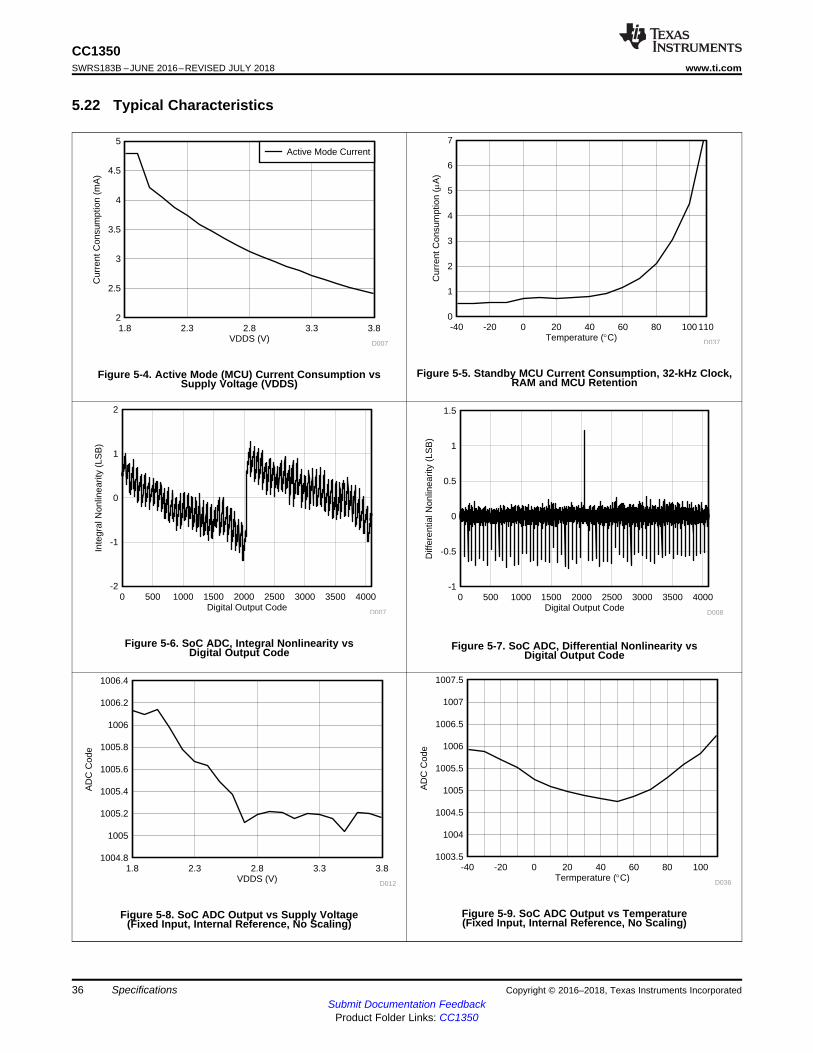
VDDS (V)
AD
C C
ode
1.8 2.3 2.8 3.3 3.81004.8
1005
1005.2
1005.4
1005.6
1005.8
1006
1006.2
1006.4
D012Termperature (qC)
AD
C C
ode
-40 -20 0 20 40 60 80 1001003.5
1004
1004.5
1005
1005.5
1006
1006.5
1007
1007.5
D036
Digital Output Code
Diff
eren
tial N
onlin
earit
y (L
SB
)
0 500 1000 1500 2000 2500 3000 3500 4000-1
-0.5
0
0.5
1
1.5
D008Digital Output Code
Inte
gral
Non
linea
rity
(LS
B)
0 500 1000 1500 2000 2500 3000 3500 4000-2
-1
0
1
2
D007
VDDS (V)
Cur
rent
Con
sum
ptio
n (m
A)
1.8 2.3 2.8 3.3 3.82
2.5
3
3.5
4
4.5
5
D007
Active Mode Current
Temperature (qC)
Cur
rent
Con
sum
ptio
n (P
A)
-40 -20 0 20 40 60 80 100 1100
1
2
3
4
5
6
7
D037
36
CC1350SWRS183B –JUNE 2016–REVISED JULY 2018 www.ti.com
Submit Documentation FeedbackProduct Folder Links: CC1350
Specifications Copyright © 2016–2018, Texas Instruments Incorporated
5.22 Typical Characteristics
Figure 5-4. Active Mode (MCU) Current Consumption vsSupply Voltage (VDDS)
Figure 5-5. Standby MCU Current Consumption, 32-kHz Clock,RAM and MCU Retention
Figure 5-6. SoC ADC, Integral Nonlinearity vsDigital Output Code Figure 5-7. SoC ADC, Differential Nonlinearity vs
Digital Output Code
Figure 5-8. SoC ADC Output vs Supply Voltage(Fixed Input, Internal Reference, No Scaling)
Figure 5-9. SoC ADC Output vs Temperature(Fixed Input, Internal Reference, No Scaling)
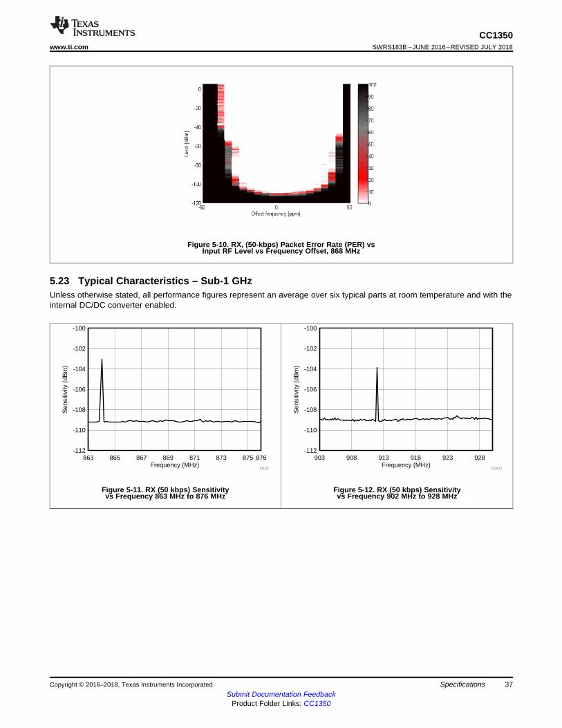
Frequency (MHz)
Sen
sitiv
ity (
dBm
)
863 865 867 869 871 873 875 876-112
-110
-108
-106
-104
-102
-100
D001Frequency (MHz)
Sen
sitiv
ity (
dBm
)
903 908 913 918 923 928-112
-110
-108
-106
-104
-102
-100
D002
37
CC1350www.ti.com SWRS183B –JUNE 2016–REVISED JULY 2018
Submit Documentation FeedbackProduct Folder Links: CC1350
SpecificationsCopyright © 2016–2018, Texas Instruments Incorporated
Figure 5-10. RX, (50-kbps) Packet Error Rate (PER) vsInput RF Level vs Frequency Offset, 868 MHz
5.23 Typical Characteristics – Sub-1 GHzUnless otherwise stated, all performance figures represent an average over six typical parts at room temperature and with theinternal DC/DC converter enabled.
Figure 5-11. RX (50 kbps) Sensitivityvs Frequency 863 MHz to 876 MHz
Figure 5-12. RX (50 kbps) Sensitivityvs Frequency 902 MHz to 928 MHz
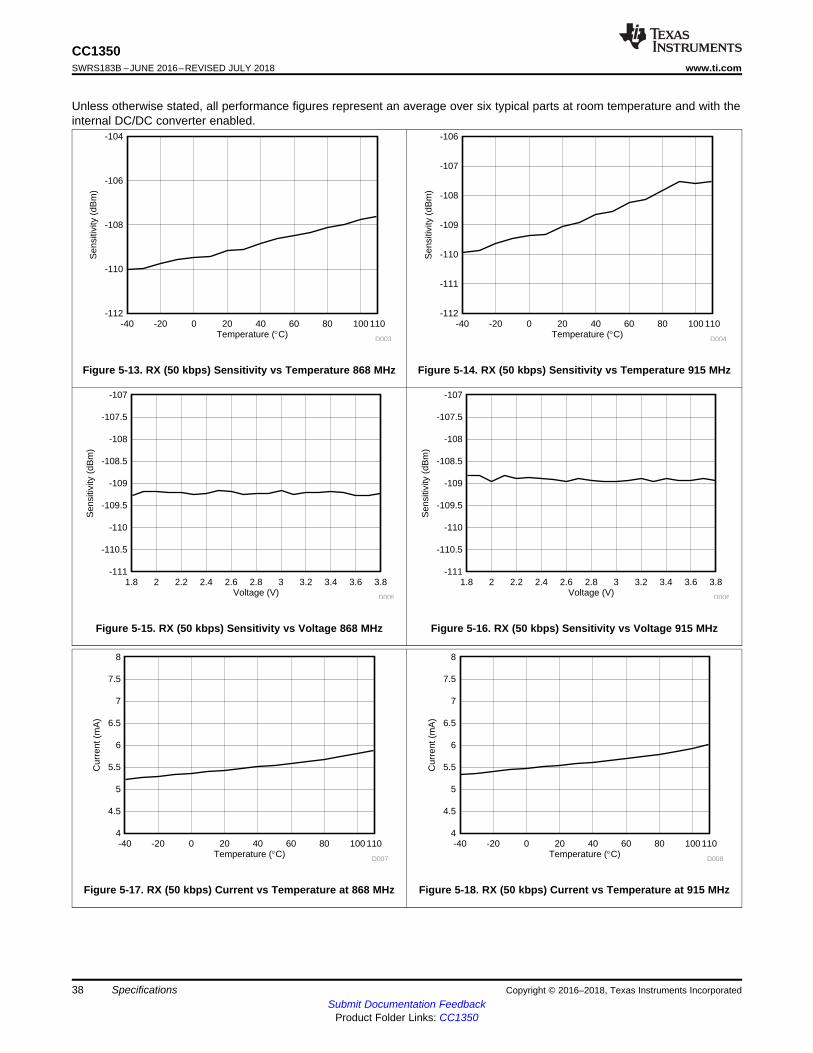
Temperature (qC)
Cur
rent
(m
A)
-40 -20 0 20 40 60 80 100 1104
4.5
5
5.5
6
6.5
7
7.5
8
D007Temperature (qC)
Cur
rent
(m
A)
-40 -20 0 20 40 60 80 100 1104
4.5
5
5.5
6
6.5
7
7.5
8
D008
Voltage (V)
Sen
sitiv
ity (
dBm
)
1.8 2 2.2 2.4 2.6 2.8 3 3.2 3.4 3.6 3.8-111
-110.5
-110
-109.5
-109
-108.5
-108
-107.5
-107
D005Voltage (V)
Sen
sitiv
ity (
dBm
)
1.8 2 2.2 2.4 2.6 2.8 3 3.2 3.4 3.6 3.8-111
-110.5
-110
-109.5
-109
-108.5
-108
-107.5
-107
D006
Temperature (qC)
Sen
sitiv
ity (
dBm
)
-40 -20 0 20 40 60 80 100 110-112
-110
-108
-106
-104
D003Temperature (qC)
Sen
sitiv
ity (
dBm
)
-40 -20 0 20 40 60 80 100 110-112
-111
-110
-109
-108
-107
-106
D004
38
CC1350SWRS183B –JUNE 2016–REVISED JULY 2018 www.ti.com
Submit Documentation FeedbackProduct Folder Links: CC1350
Specifications Copyright © 2016–2018, Texas Instruments Incorporated
Unless otherwise stated, all performance figures represent an average over six typical parts at room temperature and with theinternal DC/DC converter enabled.
Figure 5-13. RX (50 kbps) Sensitivity vs Temperature 868 MHz Figure 5-14. RX (50 kbps) Sensitivity vs Temperature 915 MHz
Figure 5-15. RX (50 kbps) Sensitivity vs Voltage 868 MHz Figure 5-16. RX (50 kbps) Sensitivity vs Voltage 915 MHz
Figure 5-17. RX (50 kbps) Current vs Temperature at 868 MHz Figure 5-18. RX (50 kbps) Current vs Temperature at 915 MHz
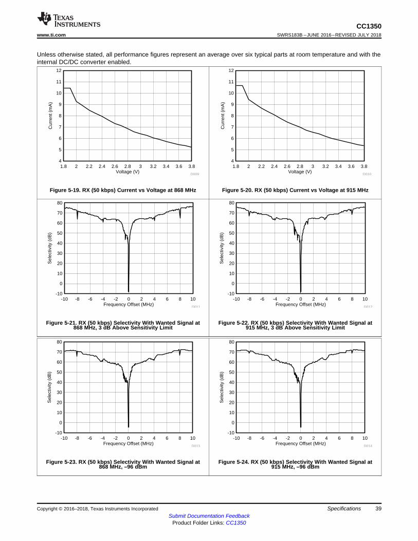
Frequency Offset (MHz)
Sel
ectiv
ity (
dB)
-10 -8 -6 -4 -2 0 2 4 6 8 10-10
0
10
20
30
40
50
60
70
80
D013Frequency Offset (MHz)
Sel
ectiv
ity (
dB)
-10 -8 -6 -4 -2 0 2 4 6 8 10-10
0
10
20
30
40
50
60
70
80
D014
Frequency Offset (MHz)
Sel
ectiv
ity (
dB)
-10 -8 -6 -4 -2 0 2 4 6 8 10-10
0
10
20
30
40
50
60
70
80
D011Frequency Offset (MHz)
Sel
ectiv
ity (
dB)
-10 -8 -6 -4 -2 0 2 4 6 8 10-10
0
10
20
30
40
50
60
70
80
D012
Voltage (V)
Cur
rent
(m
A)
1.8 2 2.2 2.4 2.6 2.8 3 3.2 3.4 3.6 3.84
5
6
7
8
9
10
11
12
D009Voltage (V)
Cur
rent
(m
A)
1.8 2 2.2 2.4 2.6 2.8 3 3.2 3.4 3.6 3.84
5
6
7
8
9
10
11
12
D010
39
CC1350www.ti.com SWRS183B –JUNE 2016–REVISED JULY 2018
Submit Documentation FeedbackProduct Folder Links: CC1350
SpecificationsCopyright © 2016–2018, Texas Instruments Incorporated
Unless otherwise stated, all performance figures represent an average over six typical parts at room temperature and with theinternal DC/DC converter enabled.
Figure 5-19. RX (50 kbps) Current vs Voltage at 868 MHz Figure 5-20. RX (50 kbps) Current vs Voltage at 915 MHz
Figure 5-21. RX (50 kbps) Selectivity With Wanted Signal at868 MHz, 3 dB Above Sensitivity Limit
Figure 5-22. RX (50 kbps) Selectivity With Wanted Signal at915 MHz, 3 dB Above Sensitivity Limit
Figure 5-23. RX (50 kbps) Selectivity With Wanted Signal at868 MHz, –96 dBm
Figure 5-24. RX (50 kbps) Selectivity With Wanted Signal at915 MHz, –96 dBm
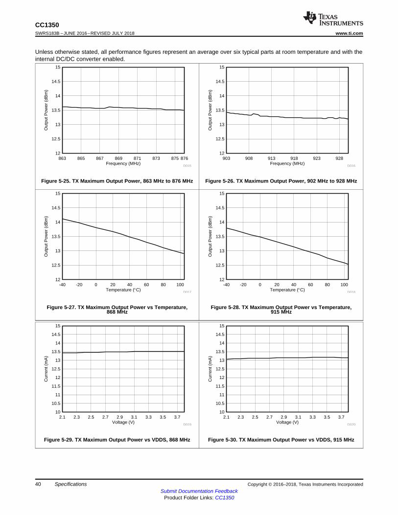
Voltage (V)
Cur
rent
(m
A)
2.1 2.3 2.5 2.7 2.9 3.1 3.3 3.5 3.710
10.5
11
11.5
12
12.5
13
13.5
14
14.5
15
D019Voltage (V)
Cur
rent
(m
A)
2.1 2.3 2.5 2.7 2.9 3.1 3.3 3.5 3.710
10.5
11
11.5
12
12.5
13
13.5
14
14.5
15
D020
Temperature (qC)
Out
put P
ower
(dB
m)
-40 -20 0 20 40 60 80 10012
12.5
13
13.5
14
14.5
15
D017Temperature (qC)
Out
put P
ower
(dB
m)
-40 -20 0 20 40 60 80 10012
12.5
13
13.5
14
14.5
15
D018
Frequency (MHz)
Out
put P
ower
(dB
m)
863 865 867 869 871 873 875 87612
12.5
13
13.5
14
14.5
15
D015Frequency (MHz)
Out
put P
ower
(dB
m)
903 908 913 918 923 92812
12.5
13
13.5
14
14.5
15
D016
40
CC1350SWRS183B –JUNE 2016–REVISED JULY 2018 www.ti.com
Submit Documentation FeedbackProduct Folder Links: CC1350
Specifications Copyright © 2016–2018, Texas Instruments Incorporated
Unless otherwise stated, all performance figures represent an average over six typical parts at room temperature and with theinternal DC/DC converter enabled.
Figure 5-25. TX Maximum Output Power, 863 MHz to 876 MHz Figure 5-26. TX Maximum Output Power, 902 MHz to 928 MHz
Figure 5-27. TX Maximum Output Power vs Temperature,868 MHz
Figure 5-28. TX Maximum Output Power vs Temperature,915 MHz
Figure 5-29. TX Maximum Output Power vs VDDS, 868 MHz Figure 5-30. TX Maximum Output Power vs VDDS, 915 MHz

Voltage (V)
Cur
rent
(m
A)
2.1 2.3 2.5 2.7 2.9 3.1 3.3 3.5 3.722
24
26
28
30
32
34
36
38
40
D025Voltage (V)
Cur
rent
(m
A)
2.1 2.3 2.5 2.7 2.9 3.1 3.3 3.5 3.722
24
26
28
30
32
34
36
38
40
D026
Temperature (qC)
Cur
rent
(m
A)
-40 -20 0 20 40 60 80 100 11022
22.5
23
23.5
24
24.5
25
25.5
26
26.5
27
D023Temperature (qC)
Cur
rent
(m
A)
-40 -20 0 20 40 60 80 100 11022
22.5
23
23.5
24
24.5
25
25.5
26
26.5
27
D024
Frequency (MHz)
Cur
rent
(m
A)
863 865 867 869 871 873 875 87623
23.5
24
24.5
25
25.5
26
D021Frequency (MHz)
Cur
rent
(m
A)
903 908 913 918 923 92823
23.5
24
24.5
25
25.5
26
D022
41
CC1350www.ti.com SWRS183B –JUNE 2016–REVISED JULY 2018
Submit Documentation FeedbackProduct Folder Links: CC1350
SpecificationsCopyright © 2016–2018, Texas Instruments Incorporated
Unless otherwise stated, all performance figures represent an average over six typical parts at room temperature and with theinternal DC/DC converter enabled.
Figure 5-31. TX Current With Maximum Output Power,863 MHz to 876 MHz
Figure 5-32. TX Current With Maximum Output Power,902 MHz to 928 MHz
Figure 5-33. TX Current With Maximum Output Powervs Temperature, 868 MHz
Figure 5-34. TX Current With Maximum Output Powervs Temperature, 915 MHz
Figure 5-35. TX Current With Maximum Output Powervs Voltage, 868 MHz
Figure 5-36. TX Current With Maximum Output Powervs Voltage, 915 MHz
SPACER

Voltage (V)
Sen
sitiv
ity (
dBm
)
1.8 2 2.2 2.4 2.6 2.8 3 3.2 3.4 3.6 3.8-90
-89
-88
-87
-86
-85
-84
-83
-82
-81
-80
D029Temperature (qC)
Cur
rent
(m
A)
-40 -20 0 20 40 60 80 100 1105
5.5
6
6.5
7
7.5
8
D030
Frequency (MHz)
Sen
sitiv
ity (
dBm
)
2400 2410 2420 2430 2440 2450 2460 2470 2480-90
-89
-88
-87
-86
-85
-84
-83
-82
-81
-80
D027Temperature (°C)
Se
nsitiv
ity
(dB
m)
-40 -20 0 20 40 60 80 100 110-90
-89
-88
-87
-86
-85
-84
-83
-82
-81
-80
D028
42
CC1350SWRS183B –JUNE 2016–REVISED JULY 2018 www.ti.com
Submit Documentation FeedbackProduct Folder Links: CC1350
Specifications Copyright © 2016–2018, Texas Instruments Incorporated
Unless otherwise stated, all performance figures represent an average over six typical parts at room temperature and with theinternal DC/DC converter enabled.
5.24 Typical Characteristics – 2.4 GHzUnless otherwise stated, all performance figures represent an average over six typical parts at room temperature and with theinternal DC/DC converter enabled.
Figure 5-37. RX Bluetooth low energy Sensitivityvs Frequency 2402 MHz to 2480 MHz
Figure 5-38. RX Bluetooth low energy Sensitivityvs Temperature 2440 MHz
Figure 5-39. RX Bluetooth low energy Sensitivityvs Voltage, 2440 MHz
Figure 5-40. RX Bluetooth low energy Currentvs Temperature at 2440 MHz

Voltage (V)
Out
put P
ower
(dB
m)
2.1 2.3 2.5 2.7 2.9 3.1 3.3 3.5 3.77
7.5
8
8.5
9
9.5
10
D035
Frequency (MHz)
Out
put P
ower
(dB
m)
2400 2410 2420 2430 2440 2450 2460 2470 24807
7.5
8
8.5
9
9.5
10
D033Temperature (qC)
Out
put P
ower
(dB
m)
-40 -20 0 20 40 60 80 100 1106
6.5
7
7.5
8
8.5
9
9.5
10
D034
Voltage (V)
Cur
rent
(m
A)
1.8 2 2.2 2.4 2.6 2.8 3 3.2 3.4 3.6 3.85
6
7
8
9
10
11
12
13
14
D031Frequency Offset (MHz)
Sel
ectiv
ity (
dB)
-40 -30 -20 -10 0 10 20 30 40 45-10
0
10
20
30
40
50
60
70
D032
43
CC1350www.ti.com SWRS183B –JUNE 2016–REVISED JULY 2018
Submit Documentation FeedbackProduct Folder Links: CC1350
SpecificationsCopyright © 2016–2018, Texas Instruments Incorporated
Unless otherwise stated, all performance figures represent an average over six typical parts at room temperature and with theinternal DC/DC converter enabled.
Figure 5-41. RX Bluetooth low energy Current vs Voltage at2440 MHz
Figure 5-42. RX Bluetooth low energy Selectivityvs Frequency Offset
Figure 5-43. TX Bluetooth low energy Maximum Output Power,2402 MHz to 2480 MHz
Figure 5-44. TX Bluetooth low energy Maximum Output Powervs Temperature, 2440 MHz
Figure 5-45. TX Bluetooth low energy Maximum Output Powervs VDDS, 2440 MHz
44
CC1350SWRS183B –JUNE 2016–REVISED JULY 2018 www.ti.com
Submit Documentation FeedbackProduct Folder Links: CC1350
Detailed Description Copyright © 2016–2018, Texas Instruments Incorporated
6 Detailed Description
6.1 OverviewSection 1.4 shows a block diagram of the core modules of the CC13xx product family.
6.2 Main CPUThe CC1350 SimpleLink Wireless MCU contains an ARM Cortex-M3 (CM3) 32-bit CPU, which runs theapplication and the higher layers of the protocol stack.
The CM3 processor provides a high-performance, low-cost platform that meets the system requirementsof minimal memory implementation and low-power consumption, while delivering outstandingcomputational performance and exceptional system response to interrupts.
The CM3 features include the following:• 32-bit ARM Cortex-M3 architecture optimized for small-footprint embedded applications• Outstanding processing performance combined with fast interrupt handling• ARM Thumb®-2 mixed 16- and 32-bit instruction set delivers the high performance expected of a 32-bit
ARM core in a compact memory size usually associated with 8- and 16-bit devices, typically in therange of a few kilobytes of memory for microcontroller-class applications:– Single-cycle multiply instruction and hardware divide– Atomic bit manipulation (bit-banding), delivering maximum memory use and streamlined peripheral
control– Unaligned data access, enabling data to be efficiently packed into memory
• Fast code execution permits slower processor clock or increases sleep mode time• Harvard architecture characterized by separate buses for instruction and data• Efficient processor core, system, and memories• Hardware division and fast digital-signal-processing oriented multiply accumulate• Saturating arithmetic for signal processing• Deterministic, high-performance interrupt handling for time-critical applications• Enhanced system debug with extensive breakpoint and trace capabilities• Serial wire trace reduces the number of pins required for debugging and tracing• Migration from the ARM7™ processor family for better performance and power efficiency• Optimized for single-cycle flash memory use• Ultra-low power consumption with integrated sleep modes• 1.25 DMIPS per MHz
45
CC1350www.ti.com SWRS183B –JUNE 2016–REVISED JULY 2018
Submit Documentation FeedbackProduct Folder Links: CC1350
Detailed DescriptionCopyright © 2016–2018, Texas Instruments Incorporated
6.3 RF CoreThe RF core is a highly flexible and capable radio system that interfaces the analog RF and basebandcircuits, handles data to and from the system side, and assembles the information bits in a given packetstructure.
The RF core can autonomously handle the time-critical aspects of the radio protocols, thus offloading themain CPU and leaving more resources for the user application. The RF core offers a high-level,command-based API to the main CPU.
The RF core supports a wide range of modulation formats, frequency bands, and accelerator features,which include the following:• Wide range of data rates:
– From 625 bps (offering long range and high robustness) to as high as 4 Mbps• Wide range of modulation formats:
– Multilevel (G) FSK and MSK– On-Off Keying (OOK) with optimized shaping to minimize adjacent channel leakage– Coding-gain support for long range
• Dedicated packet handling accelerators:– Forward error correction– Data whitening– 802.15.4g mode-switch support– Automatic CRC
• Automatic listen-before-talk (LBT) and clear channel assist (CCA)• Digital RSSI• Highly configurable channel filtering, supporting channel spacing schemes from 40 kHz to 4 MHz• High degree of flexibility, offering a future-proof solution
The RF core interfaces a highly flexible radio, with a high-performance synthesizer that can support a widerange of frequency bands.

46
CC1350SWRS183B –JUNE 2016–REVISED JULY 2018 www.ti.com
Submit Documentation FeedbackProduct Folder Links: CC1350
Detailed Description Copyright © 2016–2018, Texas Instruments Incorporated
6.4 Sensor ControllerThe Sensor Controller contains circuitry that can be selectively enabled in standby mode. The peripheralsin this domain may be controlled by the Sensor Controller Engine, which is a proprietary power-optimizedCPU. This CPU can read and monitor sensors or perform other tasks autonomously; thereby significantlyreducing power consumption and offloading the main CM3 CPU.
A PC-based development tool called Sensor Controller Studio is used to write, test, and debug code forthe Sensor Controller. The tool produces C driver source code, which the System CPU application uses tocontrol and exchange data with the Sensor Controller. Typical use cases may be (but are not limited to)the following:• Analog sensors using integrated ADC• Digital sensors using GPIOs with bit-banged I2C or SPI• Capacitive sensing• Waveform generation• Pulse counting• Key scan• Quadrature decoder for polling rotational sensors
The peripherals in the Sensor Controller include the following:• The low-power clocked comparator can be used to wake the device from any state in which the
comparator is active. A configurable internal reference can be used with the comparator. The output ofthe comparator can also be used to trigger an interrupt or the ADC.
• Capacitive sensing functionality is implemented through the use of a constant current source, a time-to-digital converter, and a comparator. The continuous time comparator in this block can also be usedas a higher-accuracy alternative to the low-power clocked comparator. The Sensor Controller takescare of baseline tracking, hysteresis, filtering, and other related functions.
• The ADC is a 12-bit, 200-ksamples/s ADC with 8 inputs and a built-in voltage reference. The ADC canbe triggered by many different sources, including timers, I/O pins, software, the analog comparator,and the RTC.
• The analog modules can be connected to up to eight different GPIOs (see Table 6-1).
The peripherals in the Sensor Controller can also be controlled from the main application processor.
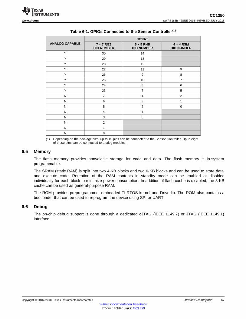
47
CC1350www.ti.com SWRS183B –JUNE 2016–REVISED JULY 2018
Submit Documentation FeedbackProduct Folder Links: CC1350
Detailed DescriptionCopyright © 2016–2018, Texas Instruments Incorporated
(1) Depending on the package size, up to 15 pins can be connected to the Sensor Controller. Up to eightof these pins can be connected to analog modules.
Table 6-1. GPIOs Connected to the Sensor Controller (1)
ANALOG CAPABLECC13x0
7 × 7 RGZDIO NUMBER
5 × 5 RHBDIO NUMBER
4 × 4 RSMDIO NUMBER
Y 30 14Y 29 13Y 28 12Y 27 11 9Y 26 9 8Y 25 10 7Y 24 8 6Y 23 7 5N 7 4 2N 6 3 1N 5 2 0N 4 1N 3 0N 2N 1N 0
6.5 MemoryThe flash memory provides nonvolatile storage for code and data. The flash memory is in-systemprogrammable.
The SRAM (static RAM) is split into two 4-KB blocks and two 6-KB blocks and can be used to store dataand execute code. Retention of the RAM contents in standby mode can be enabled or disabledindividually for each block to minimize power consumption. In addition, if flash cache is disabled, the 8-KBcache can be used as general-purpose RAM.
The ROM provides preprogrammed, embedded TI-RTOS kernel and Driverlib. The ROM also contains abootloader that can be used to reprogram the device using SPI or UART.
6.6 DebugThe on-chip debug support is done through a dedicated cJTAG (IEEE 1149.7) or JTAG (IEEE 1149.1)interface.

48
CC1350SWRS183B –JUNE 2016–REVISED JULY 2018 www.ti.com
Submit Documentation FeedbackProduct Folder Links: CC1350
Detailed Description Copyright © 2016–2018, Texas Instruments Incorporated
(1) Not including RTOS overhead.
6.7 Power ManagementTo minimize power consumption, the CC1350 device supports a number of power modes and power-management features (see Table 6-2).
Table 6-2. Power Modes
MODESOFTWARE-CONFIGURABLE POWER MODES RESET PIN
HELDACTIVE IDLE STANDBY SHUTDOWNCPU Active Off Off Off OffFlash On Available Off Off OffSRAM On On On Off OffRadio Available Available Off Off OffSupply System On On Duty Cycled Off OffCurrent 1.2 mA + 25.5 µA/MHz 570 µA 0.6 µA 185 nA 0.1 µAWake-up Time to CPU Active (1) – 14 µs 174 µs 1015 µs 1015 µsRegister Retention Full Full Partial No NoSRAM Retention Full Full Full No No
High-Speed Clock XOSC_HF orRCOSC_HF
XOSC_HF orRCOSC_HF Off Off Off
Low-Speed Clock XOSC_LF orRCOSC_LF
XOSC_LF orRCOSC_LF
XOSC_LF orRCOSC_LF Off Off
Peripherals Available Available Off Off OffSensor Controller Available Available Available Off OffWake-up on RTC Available Available Available Off OffWake-up on Pin Edge Available Available Available Available OffWake-up on Reset Pin Available Available Available Available AvailableBrown Out Detector (BOD) Active Active Duty Cycled Off N/APower On Reset (POR) Active Active Active Active N/A
In active mode, the application CM3 CPU is actively executing code. Active mode provides normaloperation of the processor and all of the peripherals that are currently enabled. The system clock can beany available clock source (see Table 6-2).
In idle mode, all active peripherals can be clocked, but the Application CPU core and memory are notclocked and no code is executed. Any interrupt event returns the processor to active mode.
In standby mode, only the always-on (AON) domain is active. An external wake-up event, RTC event, orSensor Controller event is required to return the device to active mode. MCU peripherals with retention donot need to be reconfigured when waking up again, and the CPU continues execution from where it wentinto standby mode. All GPIOs are latched in standby mode.
In shutdown mode, the device is entirely turned off (including the AON domain and Sensor Controller),and the I/Os are latched with the value they had before entering shutdown mode. A change of state onany I/O pin defined as a wake from shutdown pin wakes up the device and functions as a reset trigger.The CPU can differentiate between reset in this way and reset-by-reset pin or POR by reading the resetstatus register. The only state retained in this mode is the latched I/O state and the flash memorycontents.
The Sensor Controller is an autonomous processor that can control the peripherals in the SensorController independent of the main CPU. This means that the main CPU does not have to wake up, forexample to execute an ADC sample or poll a digital sensor over SPI, thus saving both current and wake-up time that would otherwise be wasted. The Sensor Controller Studio lets the user configure the SensorController and choose which peripherals are controlled and which conditions wake up the main CPU.

49
CC1350www.ti.com SWRS183B –JUNE 2016–REVISED JULY 2018
Submit Documentation FeedbackProduct Folder Links: CC1350
Detailed DescriptionCopyright © 2016–2018, Texas Instruments Incorporated
6.8 Clock SystemsThe CC1350 device supports two external and two internal clock sources.
A 24-MHz external crystal is required as the frequency reference for the radio. This signal is doubledinternally to create a 48-MHz clock.
The 32.768-kHz crystal is optional. The low-speed crystal oscillator is designed for use with a 32.768-kHzwatch-type crystal.
The internal high-speed RC oscillator (48-MHz) can be used as a clock source for the CPU subsystem.
The internal low-speed RC oscillator (32-kHz) can be used as a reference if the low-power crystaloscillator is not used.
The 32-kHz clock source can be used as external clocking reference through GPIO.
6.9 General Peripherals and ModulesThe I/O controller controls the digital I/O pins and contains multiplexer circuitry to assign a set ofperipherals to I/O pins in a flexible manner. All digital I/Os are interrupt and wake-up capable, have aprogrammable pullup and pulldown function, and can generate an interrupt on a negative or positive edge(configurable). When configured as an output, pins can function as either push-pull or open-drain. FiveGPIOs have high-drive capabilities, which are marked in bold in Section 4.
The SSIs are synchronous serial interfaces that are compatible with SPI, MICROWIRE, and TI'ssynchronous serial interfaces. The SSIs support both SPI master and slave up to 4 MHz.
The UART implements a universal asynchronous receiver and transmitter function. The UART supportsflexible baud-rate generation up to a maximum of 3 Mbps.
Timer 0 is a general-purpose timer module (GPTM) that provides two 16-bit timers. The GPTM can beconfigured to operate as a single 32-bit timer, dual 16-bit timers, or as a PWM module.
Timer 1, Timer 2, and Timer 3 are also GPTMs; each timer is functionally equivalent to Timer 0.
In addition to these four timers, a separate timer in the RF core handles timing for RF protocols; the RFtimer can be synchronized to the RTC.
The I2S interface is used to handle digital audio (for more information, see the CC13x0, CC26x0SimpleLink™ Wireless MCU Technical Reference Manual).
The I2C interface is used to communicate with devices compatible with the I2C standard. The I2C interfacecan handle 100-kHz and 400-kHz operation, and can serve as both I2C master and I2C slave.
The TRNG module provides a true, nondeterministic noise source for the purpose of generating keys,initialization vectors (IVs), and other random number requirements. The TRNG is built on 24 ringoscillators that create unpredictable output to feed a complex nonlinear-combinatorial circuit.
The watchdog timer is used to regain control if the system fails due to a software error after an externaldevice fails to respond as expected. The watchdog timer can generate an interrupt or a reset when apredefined time-out value is reached.

50
CC1350SWRS183B –JUNE 2016–REVISED JULY 2018 www.ti.com
Submit Documentation FeedbackProduct Folder Links: CC1350
Detailed Description Copyright © 2016–2018, Texas Instruments Incorporated
(1) The VDDS_DCDC pin must always be connected to the same voltage as the VDDS pin.
The device includes a direct memory access (µDMA) controller. The µDMA controller provides a way tooffload data-transfer tasks from the CM3 CPU, thus allowing for more efficient use of the processor andthe available bus bandwidth. The µDMA controller can perform transfer between memory and peripherals.The µDMA controller has dedicated channels for each supported on-chip module and can be programmedto automatically perform transfers between peripherals and memory when the peripheral is ready totransfer more data.
Some features of the µDMA controller follow (this is not an exhaustive list):• Highly flexible and configurable channel operation of up to 32 channels• Transfer modes: memory-to-memory, memory-to-peripheral, peripheral-to-memory, and peripheral-to-
peripheral• Data sizes of 8, 16, and 32 bits
The AON domain contains circuitry that is always enabled, except when in shutdown mode (where thedigital supply is off). This circuitry includes the following:• The RTC can be used to wake the device from any state where it is active. The RTC contains three
compare registers and one capture register. With software support, the RTC can be used for clock andcalendar operation. The RTC is clocked from the 32-kHz RC oscillator or crystal. The RTC can also becompensated to tick at the correct frequency even when the internal 32-kHz RC oscillator is usedinstead of a crystal.
• The battery monitor and temperature sensor are accessible by software and provide a battery statusindication as well as a coarse temperature measure.
6.10 Voltage Supply DomainsThe CC1350 device can interface to two or three different voltage domains depending on the packagetype. On-chip level converters ensure correct operation as long as the signal voltage on each input/outputpin is set with respect to the corresponding supply pin (VDDS, VDDS2, or VDDS3). Table 6-3 lists the pin-to-VDDS mapping.
Table 6-3. Pin Function to VDDS Mapping Table
PackageVQFN 7 × 7 (RGZ) VQFN 5 × 5 (RHB) VQFN 4 × 4 (RSM)
VDDS (1) DIO 23–30Reset_N
DIO 7–14Reset_N
DIO 5–9Reset_N
VDDS2 DIO 1–11DIO 0–6
JTAG_TCKCJTAG_TMSC
DIO 0–4JTAG_TCKCJTAG_TMSC
VDDS3DIO 12–22
JTAG_TCKCJTAG_TMSC
NA NA
6.11 System ArchitectureDepending on the product configuration, the CC1350 device can function as a wireless network processor(WNP – a device running the wireless protocol stack, with the application running on a separate hostMCU), or as a system-on-chip (SoC) with the application and protocol stack running on the ARM CM3core inside the device.
In the first case, the external host MCU communicates with the device using SPI or UART. In the secondcase, the application must be written according to the application framework supplied with the wirelessprotocol stack.

Sub-1 GHz Antenna(50 Ohm)
Pin 3/4 (RXTX)
Pin 1 (RF P)
Pin 2 (RF N)
24MHz XTAL
(Load caps on chip)
Optional inductor.
Only needed for
DCDC operation
input decoupling
To VDDR pins
VDDS_DCDC
DCDC_SW
2.4 GHz Antenna(50 Ohm)
RF Switch
Sub-1 GHz Match
2.4 GHz Match
RF_SW_CTLRF_SW_VDDS
CC 13 50
Copyright © 2016, Texas Instruments Incorporated
51
CC1350www.ti.com SWRS183B –JUNE 2016–REVISED JULY 2018
Submit Documentation FeedbackProduct Folder Links: CC1350
Application, Implementation, and LayoutCopyright © 2016–2018, Texas Instruments Incorporated
7 Application, Implementation, and Layout
NOTEInformation in the following Applications section is not part of the TI component specification,and TI does not warrant its accuracy or completeness. TI’s customers are responsible fordetermining suitability of components for their purposes. Customers should validate and testtheir design implementation to confirm system functionality.
7.1 Application InformationFew external components are required for the operation of the CC1350 device. Figure 7-1 shows a typicalapplication circuit.
The board layout greatly influences the RF performance of the CC1350 device.
On the Texas Instruments CC1350_7XD-Dual Band reference design, the optimal differential impedanceseen from the RF pins into the balun and filter and antenna is 44 + j15.
Figure 7-1 does not show decoupling capacitors for power pins. For a complete reference design, see the productfolder on www.ti.com.
Figure 7-1. CC1350 Application Circuits
52
CC1350SWRS183B –JUNE 2016–REVISED JULY 2018 www.ti.com
Submit Documentation FeedbackProduct Folder Links: CC1350
Application, Implementation, and Layout Copyright © 2016–2018, Texas Instruments Incorporated
7.2 TI Design or Reference DesignThe TI Designs Reference Design Library is a robust reference design library spanning analog, embeddedprocessor, and connectivity. Created by TI experts to help you jumpstart your system design, all TIDesigns include schematic or block diagrams, BOMs, and design files to speed your time to market.Humidity and Temperature Sensor Node for Sub-1 GHz Star Networks Enabling 10+ Year Coin Cell
Battery LifeSPACERThis reference design uses TI's nano-power system timer, boost converter, SimpleLink™ultra-low-power Sub-1GHzwireless MCU platform, and humidity-sensing technologies todemonstrate an ultra-low-power method to duty-cycle sensor end nodes leading to extremelylong battery life. The TI Design includes techniques for system design, detailed test results,and information to get the design operating running quickly.
SimpleLink™ Sub-1 GHz Sensor to Cloud Gateway Reference Design for TI-RTOS Systems SPACERThis reference design demonstrates how to connect sensors to the cloud over a long-rangeSub-1 GHz wireless network, suitable for industrial settings such as building control andasset tracking. The solution is based on a TI-RTOS gateway. This design provides acomplete end-to-end solution for creating a Sub-1 GHz sensor network with an Internet ofThings (IoT) gateway solution and cloud connectivity. The gateway solution is based on thelow-power, SimpleLink™ Wi-Fi® CC3220 wireless microcontroller (MCU), which hosts thegateway application and the SimpleLink Sub-1 GHz CC1310/CC1312R or the multi-bandCC1350/ CC1352R wireless MCU as the MAC Co-Processor. The reference design alsoincludes sensor node example applications running on the SimpleLink Sub-1 GHzCC1312R/CC1310 and multi-band CC1352R/CC1350 wireless MCUs.
Low-Power Wireless M-Bus Communications Module Reference Design SPACERThis reference design explains how to use the TI wireless M-Bus stack for CC1310 andCC1350 wireless MCUs and integrate it into a smart meter or data-collector product. Thissoftware stack is compatible with the Open Metering System (OMS) v3.0.1 specification.This design offers ready-to-use binary images for any of the wireless M-Bus S-, T-, or C-modes at 868 MHz with unidirectional (meter) or bidirectional configurations (both meter anddata collector).
Low-Power Water Flow Measurement With Inductive Sensing Reference Design SPACERThis reference design demonstrates a highly-integrated solution for this application using aninductive sensing technique enabled by the CC1310/CC1350 SimpleLink™ Wireless MCUand FemtoFET™ MOSFET. This reference design also provides the platform for integrationof wireless communications such as wireless M-Bus, Sigfox™, or a proprietary protocol.
Heat Cost Allocator with wM-Bus at 868 MHz Reference DesignSPACERThis reference design implements a heat cost allocator system following the EN834 standardwith the ‘two-sensor measurement method’. The solution achieves better than 0.5 degreesCelsius accuracy across a range of +20 to +85°C. Two analog temperature sensors areavailable as matched pairs to eliminate the need for calibration during manufacturing andlowering OEM system cost. The CC1310 wireless MCU provides a single-chip solution forheat measurement (control of the two temperature sensors) and RF communications(example code using 868 MHz wM-Bus S, T and C-modes “Meter” device).
Sub-1 GHz Sensor to Cloud Industrial IoT Gateway Reference Design for Linux Systems SPACERThis reference design demonstrates how to connect sensors to the cloud over a long-rangeSub-1 GHz wireless network, suitable for industrial settings such as building control andasset tracking. This design provides a complete end-to-end solution for creating a Sub-1GHz sensor network with an Internet of Things (IoT) gateway solution and cloud connectivity.The gateway solution is based on the low-power, SimpleLink™ Wi-Fi® CC3220 wirelessmicrocontroller (MCU), which hosts the gateway application and the SimpleLink Sub-1 GHzCC1312R/CC1310 or the multi-band CC1352R/CC1350 wireless MCU as the MAC Co-Processor.

SimpleLink™ Ultra-Low-PowerDual-Band Wireless MCU
DEVICE
PREFIX
CC1350
X = Experimental deviceBlank = Qualified device
XXX (R/T)
R = Large ReelT = Small Reel
F128
FLASH SIZE128KB
PACKAGE
RGZ = 48-pin VQFN (Very Thin Quad Flatpack No-Lead)RHB = 32-pinRSM =
VQFN32-pin VQFN
53
CC1350www.ti.com SWRS183B –JUNE 2016–REVISED JULY 2018
Submit Documentation FeedbackProduct Folder Links: CC1350
Device and Documentation SupportCopyright © 2016–2018, Texas Instruments Incorporated
Commissioning Sensors in a Sub-1 GHz Network Over Bluetooth® low energy Reference DesignSPACERThis TI Design reference design demonstrates how to easily commission a Sub-1 GHzsensor node over Bluetooth® low energy, which enables quick connectivity with asmartphone or tablet device. The design is powered by the SimpleLink™ dual-band CC1350wireless microcontroller (MCU), which is the sensor node being commissioned. There is anadded option to emulate a sensor network concentrator using a SimpleLink dual-bandCC1350 or Sub-1 GHz CC1310 devices for a complete user experience.
8 Device and Documentation Support
TI offers an extensive line of development tools. Tools and software to evaluate the performance of thedevice, generate code, and develop solutions are listed in the following.
8.1 Device NomenclatureTo designate the stages in the product development cycle, TI assigns prefixes to all part numbers and/ordate-code. Each device has one of three prefixes/identifications: X, P, or null (no prefix) (for example,CC1350 is in production; therefore, no prefix/identification is assigned).
Device development evolutionary flow:X Experimental device that is not necessarily representative of the final device's electrical
specifications and may not use production assembly flow.P Prototype device that is not necessarily the final silicon die and may not necessarily meet
final electrical specifications.null Production version of the silicon die that is fully qualified.
Production devices have been characterized fully, and the quality and reliability of the device have beendemonstrated fully. TI's standard warranty applies.
Predictions show that prototype devices (X or P) have a greater failure rate than the standard productiondevices. Texas Instruments recommends that these devices not be used in any production systembecause their expected end-use failure rate still is undefined. Only qualified production devices are to beused.
TI device nomenclature also includes a suffix with the device family name. This suffix indicates thepackage type (for example, RGZ).
For orderable part numbers of CC1350 devices in the RSM (4-mm × 4-mm), RHB (5-mm × 5-mm), orRGZ (7-mm × 7-mm) package types, see the Package Option Addendum of this document, the TI website(www.ti.com), or contact your TI sales representative.
Figure 8-1. Device Nomenclature

54
CC1350SWRS183B –JUNE 2016–REVISED JULY 2018 www.ti.com
Submit Documentation FeedbackProduct Folder Links: CC1350
Device and Documentation Support Copyright © 2016–2018, Texas Instruments Incorporated
8.2 Tools and SoftwareDevelopment Kit:Simplelink™ Dual-Band CC1350 Wireless MCU LaunchPad™ Development Kit SPACER
The CC1350 LaunchPad™ development kit combines a Bluetooth Smart radio with a Sub-1GHz radio for the ultimate combination of easy mobile phone integration with long-rangeconnectivity including a 32-bit Arm Cortex-M3 processor on a single chip. The CC1350device is a wireless MCU targeting low power, long-range wireless applications.The CC1350 device contains a 32-bit Arm Cortex-M3 processor that runs at 48 MHz as themain processor and a rich peripheral feature set that includes a unique ultra-low-powersensor controller. This sensor controller is great for interfacing external sensors and forcollecting analog and digital data autonomously while the rest of the system is in sleepmode.
Software:SimpleLink™ CC13x0 SDK SPACER
The SimpleLink™ Sub-1 GHz CC13x0 software development kit (SDK) provides acomprehensive Sub-1 GHz software package for the Sub-1 GHz CC1310 and Dual-bandCC1350 wireless MCUs and includes the following:• TI 15.4-Stack - IEEE 802.15.4e/g-based star topology networking solution for Sub-1 GHz
ISM bands (433 MHz, 868 MHz and 915 MHz).• Support for proprietary solutions - proprietary RF examples for Sub-1 GHz based on the
RF driver and EasyLink Abstraction Layer.• Bluetooth Low Energy – Stack including support for all Bluetooth core specification 4.2
features as well as a BLE micro-stack to support customers using the Dual-Band CC1350wireless MCU.
The SimpleLink CC13x0 SDK is part of the TI SimpleLink MCU platform, offering a singledevelopment environment that delivers flexible hardware, software and tool options forcustomers developing wired and wireless applications. For more information about theSimpleLink MCU Platform, visit www.ti.com/simplelink.
Software Tools:SmartRF™ Studio 7 SPACER
SmartRF™ Studio is a PC application that helps designers of radio systems to easilyevaluate the RF-IC at an early stage in the design process.• Test functions for transmitting and receiving radio packets, continuous wave transmit and
receive• Evaluate RF performance on custom boards by wiring it to a supported evaluation board
or debugger• Can also be used without any hardware, but then only to generate, edit and export radio
configuration settings• Can be used in combination with several development kits for Texas Instruments’
CC1350 RF-ICsSensor Controller Studio SPACER
Sensor Controller Studio provides a development environment for the CC1350 SensorController. The Sensor Controller is a proprietary, power-optimized CPU inside the CC1350 ,which can perform simple background tasks autonomously and independent of the SystemCPU state.• Allows for Sensor Controller task algorithms to be implemented using a C-like
programming language• Outputs a Sensor Controller Interface driver, which incorporates the generated Sensor
Controller machine code and associated definitions• Allows for rapid development by using the integrated Sensor Controller task testing and
debugging functionality. This allows for live visualization of sensor data and algorithmverification.

55
CC1350www.ti.com SWRS183B –JUNE 2016–REVISED JULY 2018
Submit Documentation FeedbackProduct Folder Links: CC1350
Device and Documentation SupportCopyright © 2016–2018, Texas Instruments Incorporated
IDEs and Compilers:Code Composer Studio™ IDE SPACER
• An integrated development environment (IDE) with project management tools and editor• Code Composer Studio (CCS) 6.1 and later has built-in support for the CC1350 device
family• Best support for XDS debuggers; XDS100v3, XDS110 and XDS200• High integration with TI-RTOS with support for TI-RTOS Object View
Code Composer Studio™ Cloud IDE SPACERCode Composer Studio™ (CCS) Cloud is a web-based IDE that allows you to create, edit,and build CCS and Energia projects. After you have successfully built your project, you candownload and run on your connected LaunchPad™ development kit. Basic debugging,including features like setting breakpoints and viewing variable values is now supported withCCS Cloud.
CCS UniFlash SPACERCCS UniFlash is a standalone tool used to program on-chip flash memory on TI MCUs.UniFlash has a GUI, command line, and scripting interface. CCS UniFlash is available free ofcharge.
IAR Embedded Workbench® for Arm• Integrated development environment with project management tools and editor• IAR EWARM 7.30.3 and later has built-in support for the CC1350 device family• Broad debugger support, supporting XDS100v3, XDS200, IAR I-jet® and SEGGER J-
Link™• Integrated development environment with project management tools and editor• RTOS plugin available for TI-RTOS
For a complete listing of development-support tools for the CC1350 platform, visit the Texas Instrumentswebsite at www.ti.com. For information on pricing and availability, contact the nearest TI field sales officeor authorized distributor.

56
CC1350SWRS183B –JUNE 2016–REVISED JULY 2018 www.ti.com
Submit Documentation FeedbackProduct Folder Links: CC1350
Device and Documentation Support Copyright © 2016–2018, Texas Instruments Incorporated
8.3 Documentation SupportTo receive notification of documentation updates, navigate to the device product folder on ti.com(CC1350). In the upper right corner, click on Alert me to register and receive a weekly digest of anyproduct information that has changed. For change details, review the revision history included in anyrevised document.
The current documentation that describes the CC1350, related peripherals, and other technical collateralis listed in the following.
ErrataCC1350 SimpleLink™ Wireless MCU Silicon Errata
Technical Reference ManualCC13xx, CC26xx SimpleLink™ Wireless MCU Technical Reference Manual
Reference GuideCC26xx/CC13xx Power Management Software Developer's Reference Guide
8.4 Texas Instruments Low-Power RF WebsiteTI's Low-Power RF website has all the latest products, application and design notes, FAQ section, newsand events updates. Go to www.ti.com/longrange.
8.5 Additional InformationTexas Instruments offers a wide selection of cost-effective, low-power RF solutions for proprietary andstandard-based wireless applications for use in industrial and consumer applications. The selectionincludes RF transceivers, RF transmitters, RF front ends, and Systems-on-Chips as well as varioussoftware solutions for the Sub-1 GHz and 2.4-GHz frequency bands.
In addition, Texas Instruments provides a large selection of support collateral such as development tools,technical documentation, reference designs, application expertise, customer support, third-party anduniversity programs.
Other than providing technical support forums, videos, and blogs, the Low-Power RF E2E OnlineCommunity also presents the opportunity to interact with engineers from all over the world.
With a broad selection of product solutions, end-application possibilities, and a range of technical support,Texas Instruments offers the broadest low-power RF portfolio.
8.6 Community ResourcesThe following links connect to TI community resources. Linked contents are provided "AS IS" by therespective contributors. They do not constitute TI specifications and do not necessarily reflect TI's views;see TI's Terms of Use.TI E2E™ Online Community The TI engineer-to-engineer (E2E) community was created to foster
collaboration among engineers. At e2e.ti.com, you can ask questions, share knowledge,explore ideas and help solve problems with fellow engineers.
TI Embedded Processors Wiki Texas Instruments Embedded Processors Wiki. Established to helpdevelopers get started with Embedded Processors from Texas Instruments and to fosterinnovation and growth of general knowledge about the hardware and software surroundingthese devices.
57
CC1350www.ti.com SWRS183B –JUNE 2016–REVISED JULY 2018
Submit Documentation FeedbackProduct Folder Links: CC1350
Mechanical, Packaging, and Orderable InformationCopyright © 2016–2018, Texas Instruments Incorporated
8.7 TrademarksSimpleLink, SmartRF, Code Composer Studio, Texas Instruments, FemtoFET, LaunchPad, E2E aretrademarks of Texas Instruments.ARM7 is a trademark of ARM Limited (or its subsidiaries).Arm, Cortex, Thumb are registered trademarks of Arm Limited (or its subsidiaries).Bluetooth, Bluetooth are registered trademarks of Bluetooth SIG, Inc.ULPBench is a trademark of Embedded Microprocessor Benchmark Consortium.CoreMark is a registered trademark of Embedded Microprocessor Benchmark Consortium.IAR Embedded Workbench, I-jet are registered trademarks of IAR Systems AB.IEEE Std 1241 is a trademark of Institute of Electrical and Electronics Engineers, Incorporated.IEEE is a registered trademark of Institute of Electrical and Electronics Engineers, Incorporated.J-Link is a trademark of SEGGER Microcontroller GmbH.Wi-Fi is a registered trademark of Wi-Fi Alliance.Wi-SUN is a trademark of Wi-SUN Alliance, Inc.Zigbee is a registered trademark of Zigbee Alliance.All other trademarks are the property of their respective owners.
8.8 Electrostatic Discharge CautionThis integrated circuit can be damaged by ESD. Texas Instruments recommends that all integrated circuits be handled withappropriate precautions. Failure to observe proper handling and installation procedures can cause damage.
ESD damage can range from subtle performance degradation to complete device failure. Precision integrated circuits may be moresusceptible to damage because very small parametric changes could cause the device not to meet its published specifications.
8.9 Export Control NoticeRecipient agrees to not knowingly export or re-export, directly or indirectly, any product or technical data(as defined by the U.S., EU, and other Export Administration Regulations) including software, or anycontrolled product restricted by other applicable national regulations, received from disclosing party undernondisclosure obligations (if any), or any direct product of such technology, to any destination to whichsuch export or re-export is restricted or prohibited by U.S. or other applicable laws, without obtaining priorauthorization from U.S. Department of Commerce and other competent Government authorities to theextent required by those laws.
8.10 GlossaryTI Glossary This glossary lists and explains terms, acronyms, and definitions.
9 Mechanical, Packaging, and Orderable Information
9.1 Packaging InformationThe following pages include mechanical packaging and orderable information. This information is the mostcurrent data available for the designated devices. This data is subject to change without notice andrevision of this document. For browser-based versions of this data sheet, refer to the left-hand navigation.
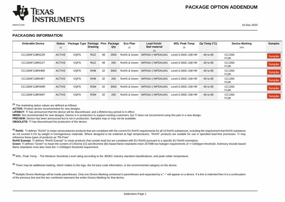
PACKAGE OPTION ADDENDUM
www.ti.com 10-Dec-2020
Addendum-Page 1
PACKAGING INFORMATION
Orderable Device Status(1)
Package Type PackageDrawing
Pins PackageQty
Eco Plan(2)
Lead finish/Ball material
(6)
MSL Peak Temp(3)
Op Temp (°C) Device Marking(4/5)
Samples
CC1350F128RGZR ACTIVE VQFN RGZ 48 2500 RoHS & Green NIPDAU | NIPDAUAG Level-3-260C-168 HR -40 to 85 CC1350F128
CC1350F128RGZT ACTIVE VQFN RGZ 48 250 RoHS & Green NIPDAU | NIPDAUAG Level-3-260C-168 HR -40 to 85 CC1350F128
CC1350F128RHBR ACTIVE VQFN RHB 32 3000 RoHS & Green NIPDAU | NIPDAUAG Level-3-260C-168 HR -40 to 85 CC1350F128
CC1350F128RHBT ACTIVE VQFN RHB 32 250 RoHS & Green NIPDAU | NIPDAUAG Level-3-260C-168 HR -40 to 85 CC1350F128
CC1350F128RSMR ACTIVE VQFN RSM 32 3000 RoHS & Green NIPDAU | NIPDAUAG Level-3-260C-168 HR -40 to 85 CC1350F128
CC1350F128RSMT ACTIVE VQFN RSM 32 250 RoHS & Green NIPDAU | NIPDAUAG Level-3-260C-168 HR -40 to 85 CC1350F128
(1) The marketing status values are defined as follows:ACTIVE: Product device recommended for new designs.LIFEBUY: TI has announced that the device will be discontinued, and a lifetime-buy period is in effect.NRND: Not recommended for new designs. Device is in production to support existing customers, but TI does not recommend using this part in a new design.PREVIEW: Device has been announced but is not in production. Samples may or may not be available.OBSOLETE: TI has discontinued the production of the device.
(2) RoHS: TI defines "RoHS" to mean semiconductor products that are compliant with the current EU RoHS requirements for all 10 RoHS substances, including the requirement that RoHS substancedo not exceed 0.1% by weight in homogeneous materials. Where designed to be soldered at high temperatures, "RoHS" products are suitable for use in specified lead-free processes. TI mayreference these types of products as "Pb-Free".RoHS Exempt: TI defines "RoHS Exempt" to mean products that contain lead but are compliant with EU RoHS pursuant to a specific EU RoHS exemption.Green: TI defines "Green" to mean the content of Chlorine (Cl) and Bromine (Br) based flame retardants meet JS709B low halogen requirements of <=1000ppm threshold. Antimony trioxide basedflame retardants must also meet the <=1000ppm threshold requirement.
(3) MSL, Peak Temp. - The Moisture Sensitivity Level rating according to the JEDEC industry standard classifications, and peak solder temperature.
(4) There may be additional marking, which relates to the logo, the lot trace code information, or the environmental category on the device.
(5) Multiple Device Markings will be inside parentheses. Only one Device Marking contained in parentheses and separated by a "~" will appear on a device. If a line is indented then it is a continuationof the previous line and the two combined represent the entire Device Marking for that device.
PACKAGE OPTION ADDENDUM
www.ti.com 10-Dec-2020
Addendum-Page 2
(6) Lead finish/Ball material - Orderable Devices may have multiple material finish options. Finish options are separated by a vertical ruled line. Lead finish/Ball material values may wrap to twolines if the finish value exceeds the maximum column width.
Important Information and Disclaimer:The information provided on this page represents TI's knowledge and belief as of the date that it is provided. TI bases its knowledge and belief on informationprovided by third parties, and makes no representation or warranty as to the accuracy of such information. Efforts are underway to better integrate information from third parties. TI has taken andcontinues to take reasonable steps to provide representative and accurate information but may not have conducted destructive testing or chemical analysis on incoming materials and chemicals.TI and TI suppliers consider certain information to be proprietary, and thus CAS numbers and other limited information may not be available for release.
In no event shall TI's liability arising out of such information exceed the total purchase price of the TI part(s) at issue in this document sold by TI to Customer on an annual basis.
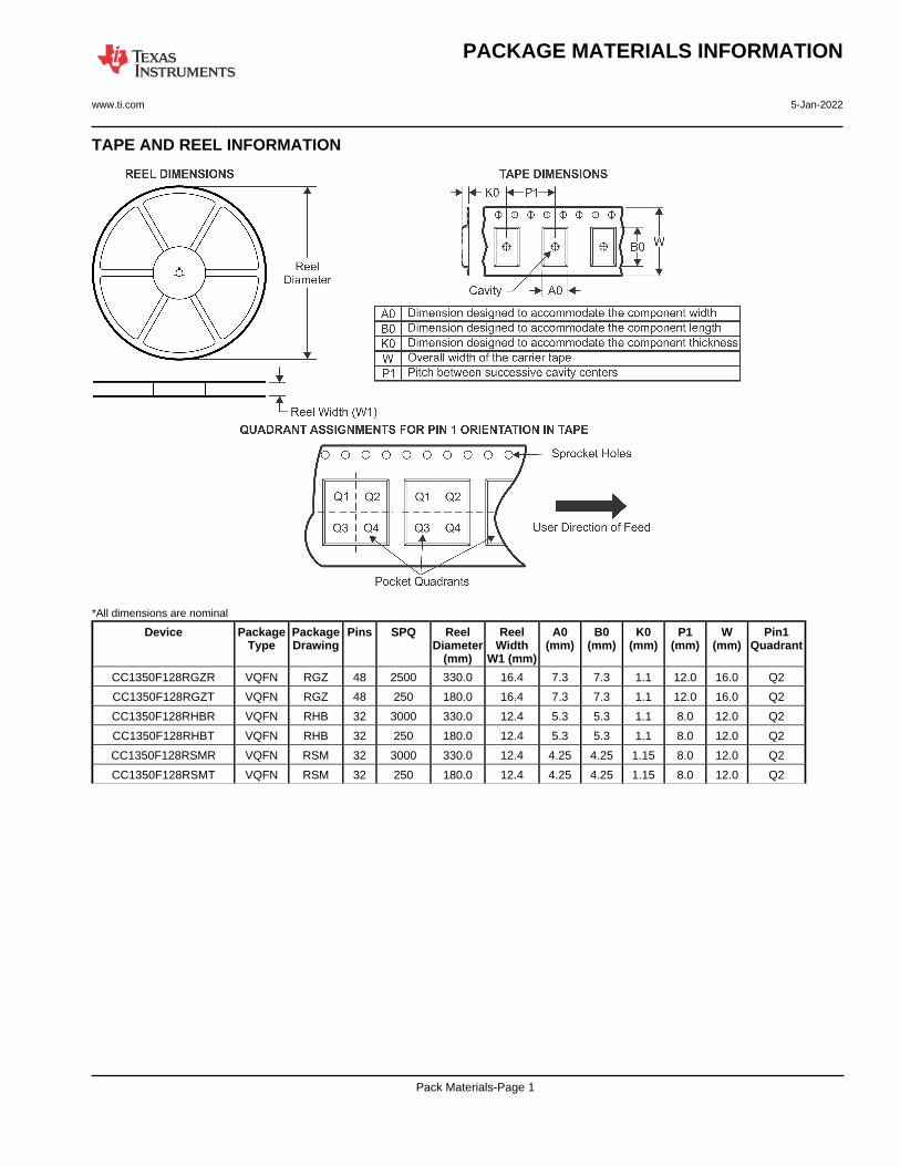
TAPE AND REEL INFORMATION
*All dimensions are nominal
Device PackageType
PackageDrawing
Pins SPQ ReelDiameter
(mm)
ReelWidth
W1 (mm)
A0(mm)
B0(mm)
K0(mm)
P1(mm)
W(mm)
Pin1Quadrant
CC1350F128RGZR VQFN RGZ 48 2500 330.0 16.4 7.3 7.3 1.1 12.0 16.0 Q2
CC1350F128RGZT VQFN RGZ 48 250 180.0 16.4 7.3 7.3 1.1 12.0 16.0 Q2
CC1350F128RHBR VQFN RHB 32 3000 330.0 12.4 5.3 5.3 1.1 8.0 12.0 Q2
CC1350F128RHBT VQFN RHB 32 250 180.0 12.4 5.3 5.3 1.1 8.0 12.0 Q2
CC1350F128RSMR VQFN RSM 32 3000 330.0 12.4 4.25 4.25 1.15 8.0 12.0 Q2
CC1350F128RSMT VQFN RSM 32 250 180.0 12.4 4.25 4.25 1.15 8.0 12.0 Q2
PACKAGE MATERIALS INFORMATION
www.ti.com 5-Jan-2022
Pack Materials-Page 1
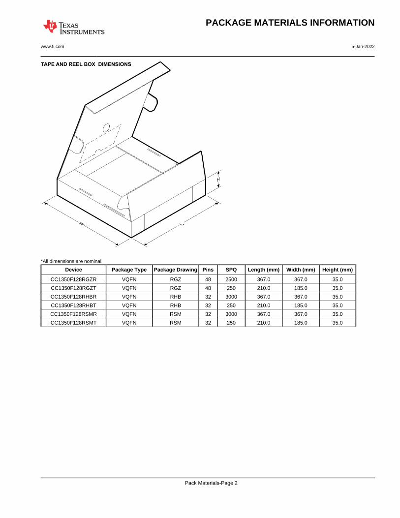
*All dimensions are nominal
Device Package Type Package Drawing Pins SPQ Length (mm) Width (mm) Height (mm)
CC1350F128RGZR VQFN RGZ 48 2500 367.0 367.0 35.0
CC1350F128RGZT VQFN RGZ 48 250 210.0 185.0 35.0
CC1350F128RHBR VQFN RHB 32 3000 367.0 367.0 35.0
CC1350F128RHBT VQFN RHB 32 250 210.0 185.0 35.0
CC1350F128RSMR VQFN RSM 32 3000 367.0 367.0 35.0
CC1350F128RSMT VQFN RSM 32 250 210.0 185.0 35.0
PACKAGE MATERIALS INFORMATION
www.ti.com 5-Jan-2022
Pack Materials-Page 2
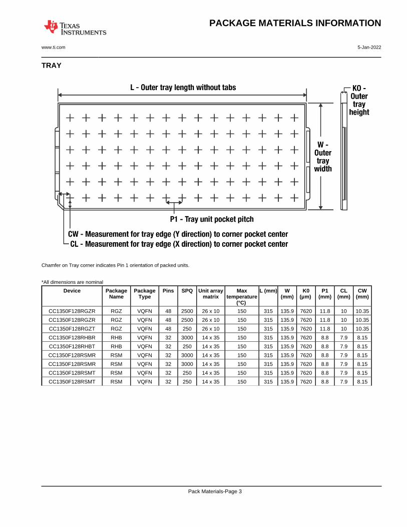
TRAY
Chamfer on Tray corner indicates Pin 1 orientation of packed units.
*All dimensions are nominal
Device PackageName
PackageType
Pins SPQ Unit arraymatrix
Maxtemperature
(°C)
L (mm) W(mm)
K0(µm)
P1(mm)
CL(mm)
CW(mm)
CC1350F128RGZR RGZ VQFN 48 2500 26 x 10 150 315 135.9 7620 11.8 10 10.35
CC1350F128RGZR RGZ VQFN 48 2500 26 x 10 150 315 135.9 7620 11.8 10 10.35
CC1350F128RGZT RGZ VQFN 48 250 26 x 10 150 315 135.9 7620 11.8 10 10.35
CC1350F128RHBR RHB VQFN 32 3000 14 x 35 150 315 135.9 7620 8.8 7.9 8.15
CC1350F128RHBT RHB VQFN 32 250 14 x 35 150 315 135.9 7620 8.8 7.9 8.15
CC1350F128RSMR RSM VQFN 32 3000 14 x 35 150 315 135.9 7620 8.8 7.9 8.15
CC1350F128RSMR RSM VQFN 32 3000 14 x 35 150 315 135.9 7620 8.8 7.9 8.15
CC1350F128RSMT RSM VQFN 32 250 14 x 35 150 315 135.9 7620 8.8 7.9 8.15
CC1350F128RSMT RSM VQFN 32 250 14 x 35 150 315 135.9 7620 8.8 7.9 8.15
PACKAGE MATERIALS INFORMATION
www.ti.com 5-Jan-2022
Pack Materials-Page 3

www.ti.com
GENERIC PACKAGE VIEW
Images above are just a representation of the package family, actual package may vary.Refer to the product data sheet for package details.
VQFN - 1 mm max heightRGZ 48PLASTIC QUADFLAT PACK- NO LEAD7 x 7, 0.5 mm pitch
4224671/A
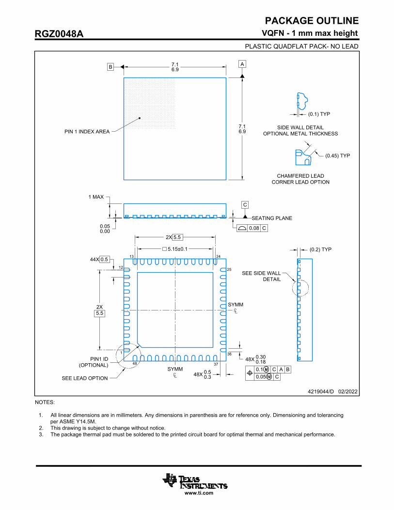
NOTES:
1. All linear dimensions are in millimeters. Any dimensions in parenthesis are for reference only. Dimensioning and tolerancingper ASME Y14.5M.
2. This drawing is subject to change without notice.3. The package thermal pad must be soldered to the printed circuit board for optimal thermal and mechanical performance.
PACKAGE OUTLINE
4219044/D 02/2022
www.ti.com
VQFN - 1 mm max heightPLASTIC QUADFLAT PACK- NO LEAD
RGZ0048A
A
0.08 C
0.1 C A B0.05 C
B
SYMM
SYMM
PIN 1 INDEX AREA
7.16.9
7.16.9
1 MAX
0.050.00
SEATING PLANE
C
5.15±0.1
2X 5.5
2X5.5
44X 0.5
48X 0.50.3
48X 0.300.18PIN1 ID
(OPTIONAL)
(0.2) TYP
1
12
13 24
25
36
3748
(0.1) TYP
SIDE WALL DETAILOPTIONAL METAL THICKNESS
SEE SIDE WALLDETAIL
CHAMFERED LEADCORNER LEAD OPTION
(0.45) TYP
SEE LEAD OPTION
AutoCAD SHX Text
AutoCAD SHX Text

NOTES: (continued)
4. This package is designed to be soldered to a thermal pad on the board. For more information, see Texas Instruments literaturenumber SLUA271 (www.ti.com/lit/slua271).
5. Vias are optional depending on application, refer to device data sheet. If any vias are implemented, refer to their locations shown on this view. It is recommended that vias under paste be filled, plugged or tented.
EXAMPLE BOARD LAYOUT
4219044/D 02/2022
www.ti.com
VQFN - 1 mm max heightRGZ0048APLASTIC QUADFLAT PACK- NO LEAD
SYMM
SYMM
LAND PATTERN EXAMPLESCALE: 15X
( 5.15)
2X (6.8)
2X(6.8)
48X (0.6)
48X (0.24)
44X (0.5)
2X (5.5)
2X(5.5)
21X (Ø0.2) VIATYP
(R0.05)TYP
NON SOLDER MASKDEFINED
(PREFERRED)
SOLDER MASKDEFINED
METAL
SOLDER MASKOPENING
EXPOSED METAL
SOLDER MASK DETAILS
SOLDER MASKOPENING
METAL UNDERSOLDER MASK
EXPOSED METAL
0.07 MAXALL AROUND
0.07 MINALL AROUND
2X(1.26)
2X (1.26) 2X (1.065)
2X(1.065)
1
12
13 24
25
36
3748
AutoCAD SHX Text
AutoCAD SHX Text
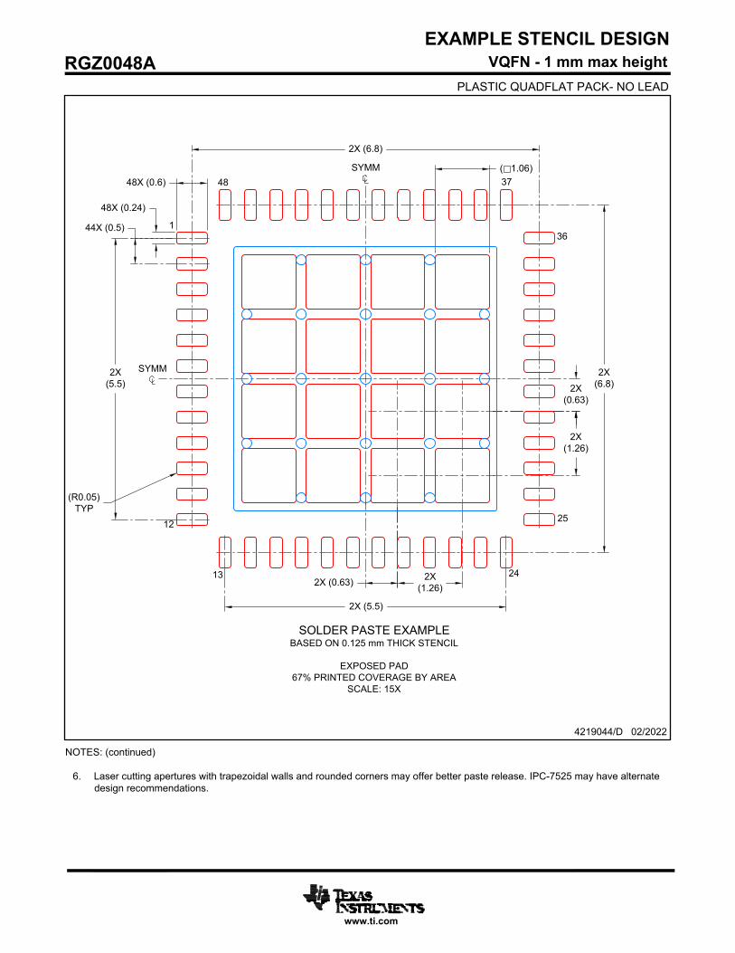
NOTES: (continued)
6. Laser cutting apertures with trapezoidal walls and rounded corners may offer better paste release. IPC-7525 may have alternatedesign recommendations.
EXAMPLE STENCIL DESIGN
4219044/D 02/2022
www.ti.com
VQFN - 1 mm max heightRGZ0048APLASTIC QUADFLAT PACK- NO LEAD
SOLDER PASTE EXAMPLEBASED ON 0.125 mm THICK STENCIL
EXPOSED PAD67% PRINTED COVERAGE BY AREA
SCALE: 15X
SYMM
SYMM ( 1.06)
2X (6.8)
2X(6.8)
48X (0.6)
48X (0.24)
44X (0.5)
2X (5.5)
2X(5.5)
(R0.05)TYP
2X(0.63)
2X (0.63) 2X(1.26)
2X(1.26)
1
12
13 24
25
36
3748
AutoCAD SHX Text
AutoCAD SHX Text

www.ti.com
GENERIC PACKAGE VIEW
This image is a representation of the package family, actual package may vary.Refer to the product data sheet for package details.
VQFN - 1 mm max heightRSM 32PLASTIC QUAD FLATPACK - NO LEAD4 x 4, 0.4 mm pitch
4224982/A

www.ti.com
PACKAGE OUTLINE
C
32X 0.250.15
2.8 0.05
32X 0.450.25
1 MAX
(0.2) TYP
0.050.00
28X 0.4
2X2.8
2X 2.8
A 4.13.9
B
4.13.9
0.250.15
0.450.25
4X (0.45)
(0.1)
VQFN - 1 mm max heightRSM0032BPLASTIC QUAD FLATPACK - NO LEAD
4219108/B 08/2019
PIN 1 INDEX AREA
0.08 C
SEATING PLANE
1
817
24
9 16
32 25(OPTIONAL)
PIN 1 ID0.1 C A B0.05
EXPOSEDTHERMAL PAD
DETAILSEE TERMINAL
SYMM
SYMM
NOTES: 1. All linear dimensions are in millimeters. Any dimensions in parenthesis are for reference only. Dimensioning and tolerancing per ASME Y14.5M. 2. This drawing is subject to change without notice. 3. The package thermal pad must be soldered to the printed circuit board for thermal and mechanical performance.
33
SEE SIDE WALLDETAIL
SIDE WALL DETAILOPTIONAL METAL THICKNESS
SCALE 3.000
DETAILOPTIONAL TERMINAL
TYPICAL

www.ti.com
EXAMPLE BOARD LAYOUT
0.05 MINALL AROUND
0.05 MAXALL AROUND
32X (0.2)
32X (0.55)
( 0.2) TYPVIA
28X (0.4)
(3.85)
(3.85)
( 2.8)
(R0.05)TYP
(1.15)
(1.15)
VQFN - 1 mm max heightRSM0032BPLASTIC QUAD FLATPACK - NO LEAD
4219108/B 08/2019
SYMM
1
8
9 16
17
24
2532
SYMM
LAND PATTERN EXAMPLEEXPOSED METAL SHOWN
SCALE:20X
33
NOTES: (continued) 4. This package is designed to be soldered to a thermal pad on the board. For more information, see Texas Instruments literature number SLUA271 (www.ti.com/lit/slua271).5. Vias are optional depending on application, refer to device data sheet. If any vias are implemented, refer to their locations shown on this view. It is recommended that vias under paste be filled, plugged or tented.
SOLDER MASKOPENING
METAL UNDERSOLDER MASK
SOLDER MASKDEFINED
EXPOSED METALMETAL
SOLDER MASKOPENING
SOLDER MASK DETAILS
NON SOLDER MASKDEFINED
(PREFERRED)
EXPOSED METAL
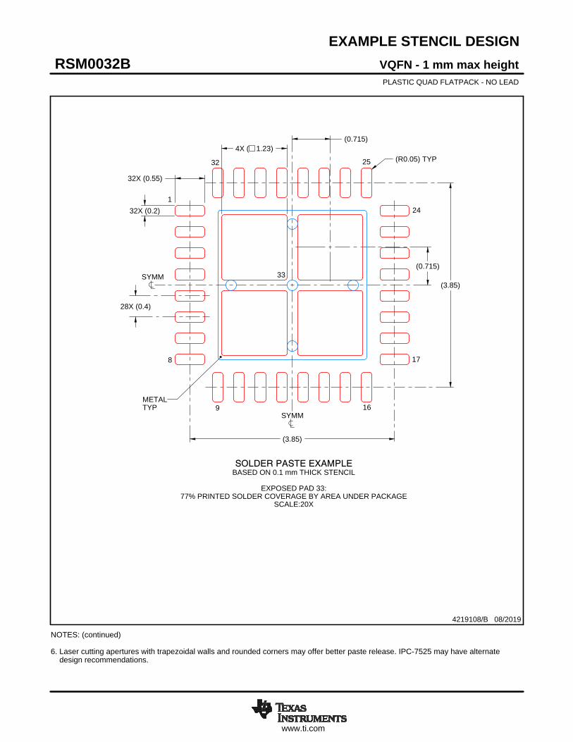
www.ti.com
EXAMPLE STENCIL DESIGN
32X (0.55)
32X (0.2)
28X (0.4)
(3.85)
(3.85)
4X ( 1.23)(R0.05) TYP
(0.715)
(0.715)
VQFN - 1 mm max heightRSM0032BPLASTIC QUAD FLATPACK - NO LEAD
4219108/B 08/2019
NOTES: (continued) 6. Laser cutting apertures with trapezoidal walls and rounded corners may offer better paste release. IPC-7525 may have alternate design recommendations.
33
SYMM
METALTYP
SOLDER PASTE EXAMPLEBASED ON 0.1 mm THICK STENCIL
EXPOSED PAD 33:
77% PRINTED SOLDER COVERAGE BY AREA UNDER PACKAGESCALE:20X
SYMM
1
8
9 16
17
24
2532
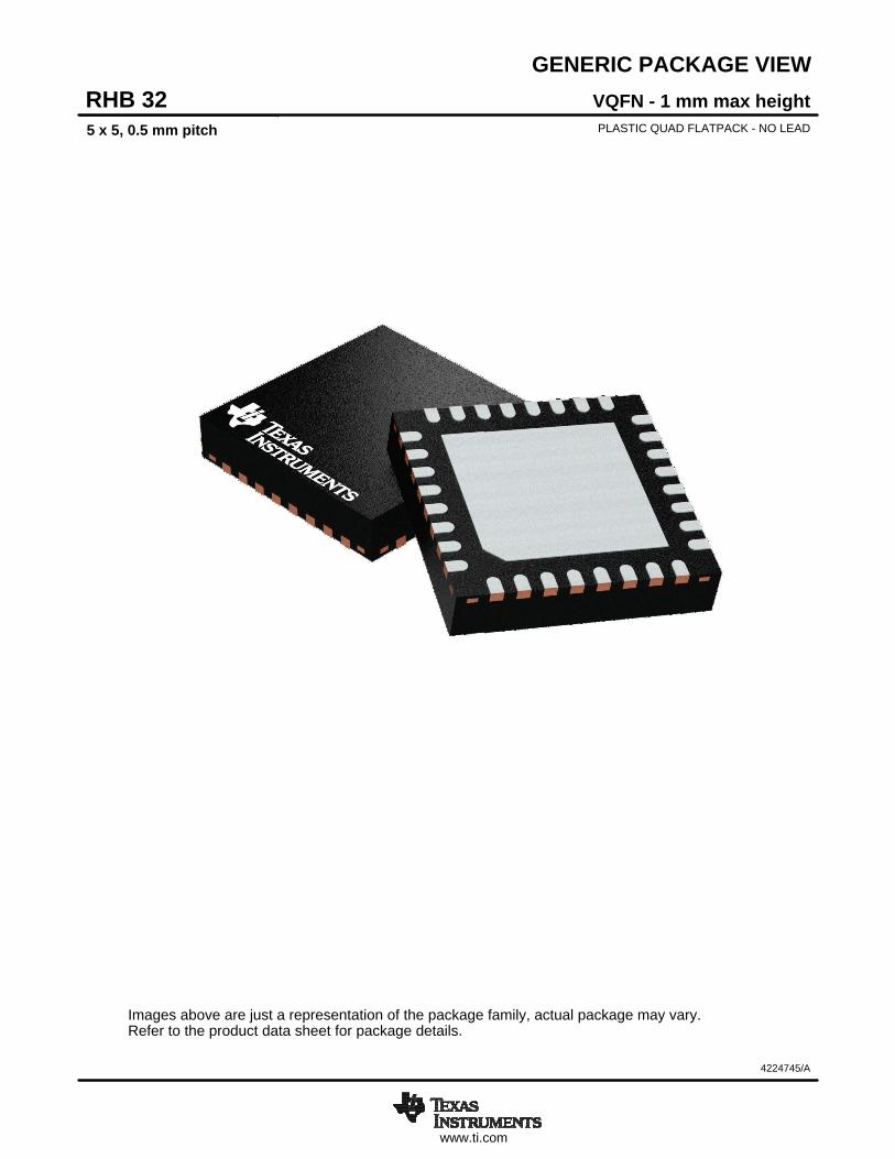
www.ti.com
GENERIC PACKAGE VIEW
Images above are just a representation of the package family, actual package may vary.Refer to the product data sheet for package details.
VQFN - 1 mm max heightRHB 32PLASTIC QUAD FLATPACK - NO LEAD5 x 5, 0.5 mm pitch
4224745/A

www.ti.com
PACKAGE OUTLINE
C
32X 0.30.2
3.45 0.1
32X 0.50.3
1 MAX
(0.2) TYP
0.050.00
28X 0.5
2X3.5
2X 3.5
A 5.14.9
B
5.14.9
(0.1)
VQFN - 1 mm max heightRHB0032EPLASTIC QUAD FLATPACK - NO LEAD
4223442/B 08/2019
PIN 1 INDEX AREA
0.08 C
SEATING PLANE
1
817
24
9 16
32 25
(OPTIONAL)PIN 1 ID
0.1 C A B0.05 C
EXPOSEDTHERMAL PAD
33 SYMM
SYMM
NOTES: 1. All linear dimensions are in millimeters. Any dimensions in parenthesis are for reference only. Dimensioning and tolerancing per ASME Y14.5M. 2. This drawing is subject to change without notice. 3. The package thermal pad must be soldered to the printed circuit board for thermal and mechanical performance.
SCALE 3.000
SEE SIDE WALLDETAIL
20.000
SIDE WALL DETAILOPTIONAL METAL THICKNESS
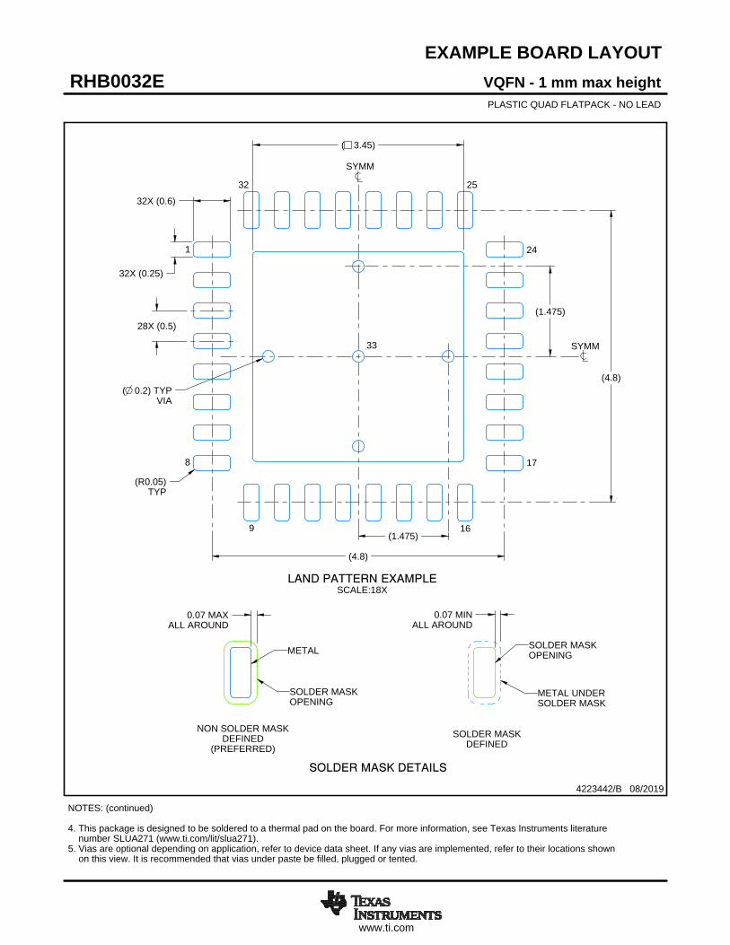
www.ti.com
EXAMPLE BOARD LAYOUT
(1.475)
0.07 MINALL AROUND
0.07 MAXALL AROUND
32X (0.25)
32X (0.6)
( 0.2) TYPVIA
28X (0.5)
(4.8)
(4.8)
(1.475)
( 3.45)
(R0.05)TYP
VQFN - 1 mm max heightRHB0032EPLASTIC QUAD FLATPACK - NO LEAD
4223442/B 08/2019
SYMM
1
8
9 16
17
24
2532
SYMM
LAND PATTERN EXAMPLESCALE:18X
NOTES: (continued) 4. This package is designed to be soldered to a thermal pad on the board. For more information, see Texas Instruments literature number SLUA271 (www.ti.com/lit/slua271).5. Vias are optional depending on application, refer to device data sheet. If any vias are implemented, refer to their locations shown on this view. It is recommended that vias under paste be filled, plugged or tented.
33
SOLDER MASKOPENING
METAL UNDERSOLDER MASK
SOLDER MASKDEFINED
METAL
SOLDER MASKOPENING
SOLDER MASK DETAILS
NON SOLDER MASKDEFINED
(PREFERRED)
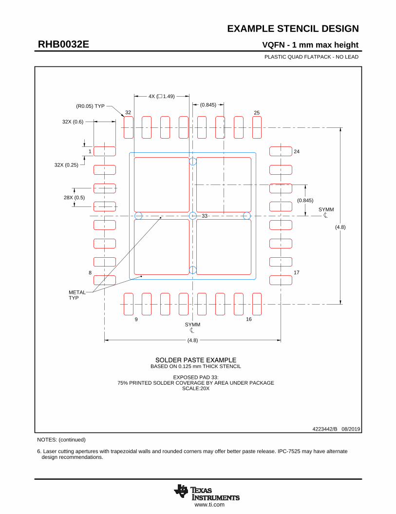
www.ti.com
EXAMPLE STENCIL DESIGN
32X (0.6)
32X (0.25)
28X (0.5)
(4.8)
(4.8)
4X ( 1.49)
(0.845)
(0.845)(R0.05) TYP
VQFN - 1 mm max heightRHB0032EPLASTIC QUAD FLATPACK - NO LEAD
4223442/B 08/2019
NOTES: (continued) 6. Laser cutting apertures with trapezoidal walls and rounded corners may offer better paste release. IPC-7525 may have alternate design recommendations.
33
SYMM
METALTYP
SOLDER PASTE EXAMPLEBASED ON 0.125 mm THICK STENCIL
EXPOSED PAD 33:
75% PRINTED SOLDER COVERAGE BY AREA UNDER PACKAGESCALE:20X
SYMM
1
8
9 16
17
24
2532

IMPORTANT NOTICE AND DISCLAIMERTI PROVIDES TECHNICAL AND RELIABILITY DATA (INCLUDING DATA SHEETS), DESIGN RESOURCES (INCLUDING REFERENCE DESIGNS), APPLICATION OR OTHER DESIGN ADVICE, WEB TOOLS, SAFETY INFORMATION, AND OTHER RESOURCES “AS IS” AND WITH ALL FAULTS, AND DISCLAIMS ALL WARRANTIES, EXPRESS AND IMPLIED, INCLUDING WITHOUT LIMITATION ANY IMPLIED WARRANTIES OF MERCHANTABILITY, FITNESS FOR A PARTICULAR PURPOSE OR NON-INFRINGEMENT OF THIRD PARTY INTELLECTUAL PROPERTY RIGHTS.These resources are intended for skilled developers designing with TI products. You are solely responsible for (1) selecting the appropriate TI products for your application, (2) designing, validating and testing your application, and (3) ensuring your application meets applicable standards, and any other safety, security, regulatory or other requirements.These resources are subject to change without notice. TI grants you permission to use these resources only for development of an application that uses the TI products described in the resource. Other reproduction and display of these resources is prohibited. No license is granted to any other TI intellectual property right or to any third party intellectual property right. TI disclaims responsibility for, and you will fully indemnify TI and its representatives against, any claims, damages, costs, losses, and liabilities arising out of your use of these resources.TI’s products are provided subject to TI’s Terms of Sale or other applicable terms available either on ti.com or provided in conjunction with such TI products. TI’s provision of these resources does not expand or otherwise alter TI’s applicable warranties or warranty disclaimers for TI products.TI objects to and rejects any additional or different terms you may have proposed. IMPORTANT NOTICE
Mailing Address: Texas Instruments, Post Office Box 655303, Dallas, Texas 75265Copyright © 2022, Texas Instruments Incorporated